

Page 1

<Dual-In-Line Package Intelligent Power Module>
1200V Mini DIPIPM with BSD Series APPLICATION NOTE
PSS**S72FT
Table of contents
CHAPTER 1 INTRODUCTION .................................................................................................................................2
1.1 Features of 1200V Mini DIPIPM with BSD ............................................................................................................. 2
1.2 Functions ............................................................................................................................................................... 3
1.3 Target Applications ................................................................................................................................................. 4
1.4 Product Line-up ...................................................................................................................................................... 4
CHAPTER 2 SPECIFICATIONS AND CHARACTERISTICS ....................................................................................5
2.1 1200V Mini DIPIPM with BSD Specifications ......................................................................................................... 5
2.1.1 Maximum Ratings .............................................................................................................................................................................................. 5
2.1.2 Thermal Resistance ........................................................................................................................................................................................... 7
2.1.3 Electric Characteristics and Recommended Conditions ..................................................................................................................................... 8
2.1.4 Mechanical Characteristics and Ratings .......................................................................................................................................................... 10
2.2 Protective Functions and Operating Sequence ..................................................................................................... 11
2.2.1 Short Circuit Protection .................................................................................................................................................................................... 11
2.2.2 Control Supply UV Protection .......................................................................................................................................................................... 13
2.2.3 Temperature output function VOT ...................................................................................................................................................................... 15
2.3 Package Outlines ................................................................................................................................................. 20
2.3.1 Package outlines.............................................................................................................................................................................................. 20
2.3.2 Marking ............................................................................................................................................................................................................ 21
The Lot number indicates production year, month, running number and country of origin. ........................................................................................ 21
2.3.3 Terminal Description ........................................................................................................................................................................................ 22
2.4 Mounting Method ................................................................................................................................................. 24
2.4.1 Electric Spacing ............................................................................................................................................................................................... 24
2.4.2 Mounting Method and Precautions ................................................................................................................................................................... 24
2.4.3 Soldering Conditions ........................................................................................................................................................................................ 25
CHAPTER 3 SYSTEM APPLICATION GUIDANCE ................................................................................................27
3.1 Application Guidance ........................................................................................................................................... 27
3.1.1 System connection ........................................................................................................................................................................................... 27
3.1.2 Interface Circuit (Direct Coupling Interface example for using one shunt resistor) ........................................................................................... 28
3.1.3 Interface Circuit (Example of Opto-coupler Isolated Interface) ......................................................................................................................... 29
3.1.4 External SC Protection Circuit with Using Three Shunt Resistors .................................................................................................................... 30
3.1.5 Circuits of Signal Input Terminals and Fo Terminal ........................................................................................................................................... 30
3.1.6 Snubber Circuit ................................................................................................................................................................................................ 32
3.1.7 Recommended Wiring Method around Shunt Resistor..................................................................................................................................... 33
3.1.8 Precaution for Wiring on PCB .......................................................................................................................................................................... 35
3.1.9 Parallel operation of DIPIPM ............................................................................................................................................................................ 36
3.1.10 SOA of Mini DIPIPM ....................................................................................................................................................................................... 36
3.1.11 SCSOA .......................................................................................................................................................................................................... 37
3.1.12 Power Life Cycles .......................................................................................................................................................................................... 38
3.2 Power Loss and Thermal Dissipation Calculation ................................................................................................ 39
3.2.1 Power Loss Calculation ................................................................................................................................................................................... 39
3.2.2 Temperature Rise Considerations and Calculation Example ............................................................................................................................ 41
3.3.1 Evaluation Circuit of Noise Withstand Capability .............................................................................................................................................. 42
3.3.2 Countermeasures and Precautions .................................................................................................................................................................. 42
3.3.3 Static Electricity Withstand Capability ............................................................................................................................................................... 43
CHAPTER 4 Bootstrap Circuit Operation................................................................................................................44
4.1 Bootstrap Circuit Operation .................................................................................................................................. 44
4.2 Bootstrap Supply Circuit Current at Switching State ............................................................................................ 45
4.3 Note for designing the bootstrap circuit ................................................................................................................ 46
4.4 Initial charging in bootstrap circuit ........................................................................................................................ 47
CHAPTER 5 PACKAGE HANDLING ......................................................................................................................48
5.1 Packaging Specification ....................................................................................................................................... 48
5.2 Handling Precautions ........................................................................................................................................... 49
Publication Date: September 2015
1
Page 2
<Dual-In-Line Package Intelligent Power Module>
1200V Mini DIPIPM with BSD Series APPLICATION NOTE
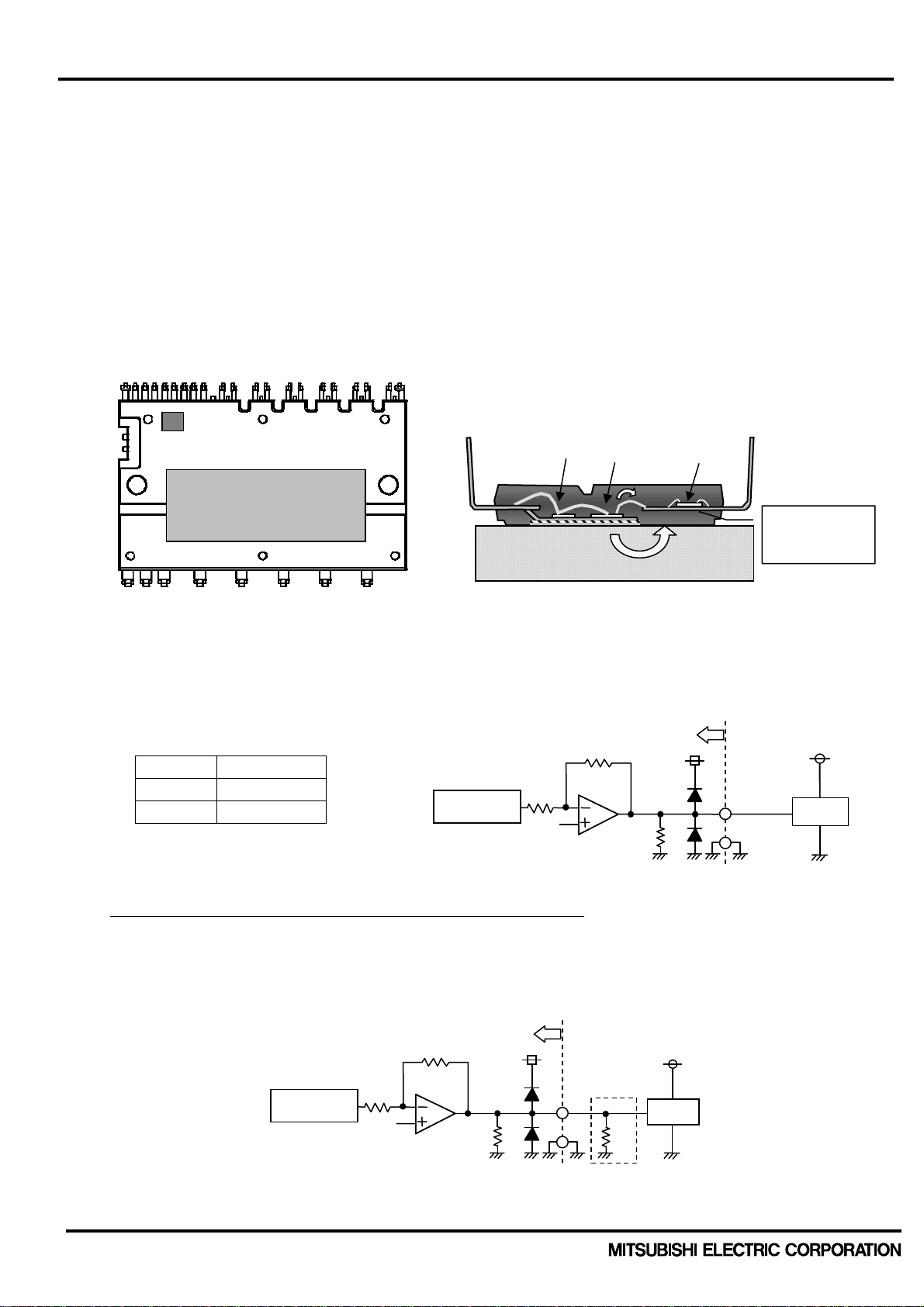
CHAPTER 1 INTRODUCTION
1.1 Features of 1200V Mini DIPIPM with BSD
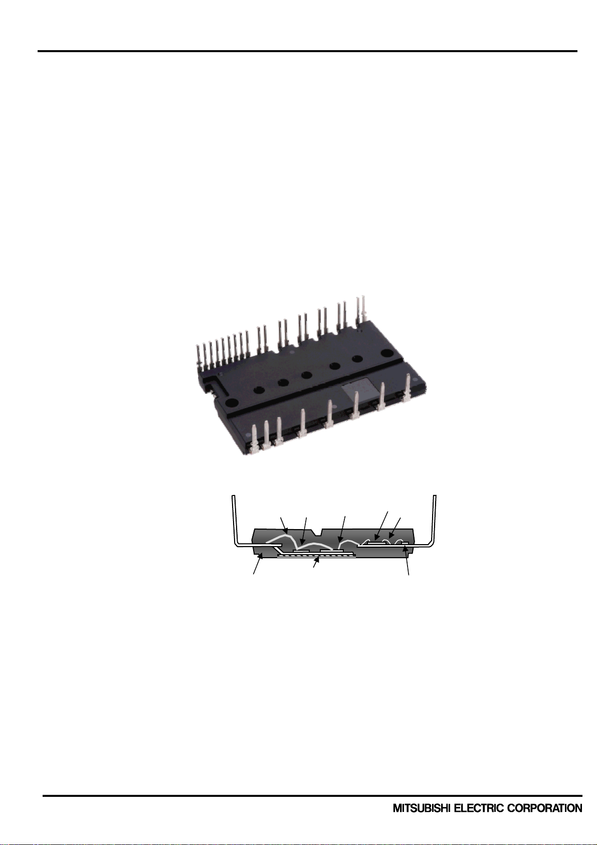
Mini DIPIPM with BSD is an ultra-small compact intelligent power module with transfer mold package
favorable for larger mass production. Power chips, drive and protection circuits are integrated in the module,
which make it easy for AC400-440V class low power motor inverter control. It includes many improvements
(loss performance, built-in peripheral functions and line-up expansion). Main features of this series are as
below.
・Newly developed 6th generation CSTBT are integrated for improving efficiency
・Incorporating bootstrap diode(BSD) with current limiting resistor for P-side gate driving supply
・Newly integrated temperature of control IC part output function
・Same package with Mini DIPIPM with BSD Series.
About detailed differences, please refer Section 1.5. Fig.1-1-1 and Fig.1-1-2 show the outline and internal
cross-section structure respectively.
Fig.1-1-1 Package image
Cu frame
Molding resin
Al wire
FWDi
Insulation sheet
(copper foil+ resin)
IGBT
IC
Au wire
BSD
Fig.1-1-2 Internal cross-section structure
Publication Date: September 2015
2
Page 3
<Dual-In-Line Package Intelligent Power Module>
T
1200V Mini DIPIPM with BSD Series APPLICATION NOTE
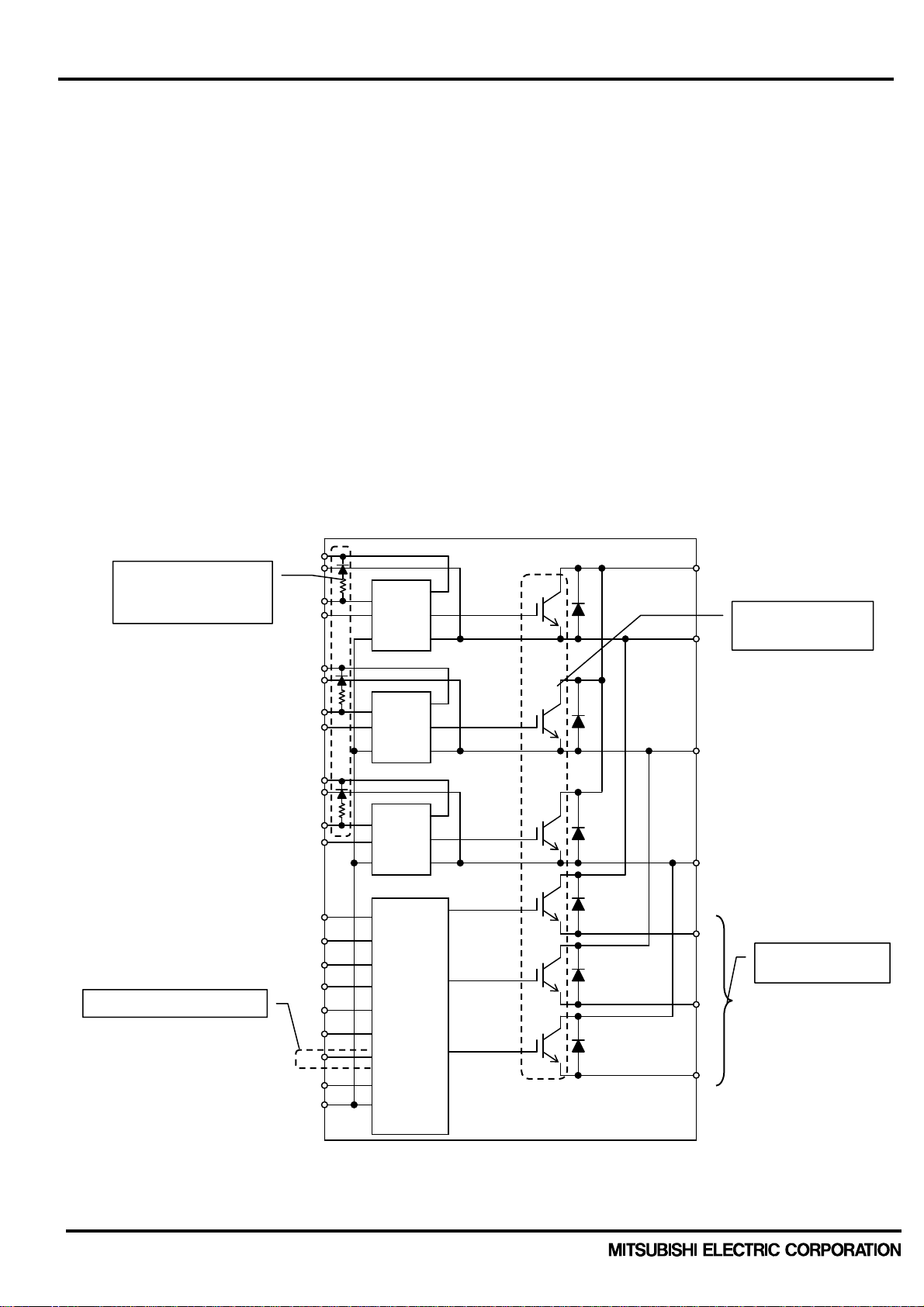
1.2 Functions
1200V Mini DIPIPM has following functions and inner block diagram is described in Fig.1-2-1.
● For P-side IGBTs:
- Drive circuit;
- High voltage level shift circuit;
- Control supply under voltage (UV) lockout circuit (without fault signal output).
- Built-in bootstrap diode (BSD) with current limiting resistor
● For N-side IGBTs:
-Drive circuit;
-Short circuit (SC) protection circuit (by inserting external shunt resistor into main current path)
-Control supply under voltage (UV) lockout circuit (with fault signal output)
-Outputting LVIC temperature by analog signal (No self over temperature protection)
● Fault Signal Output
-Corresponding to N-side IGBT SC and N-side UV protection.
● IGBT Drive Supply
-Single DC15V power supply (in the case of using bootstrap method)
● Control Input Interface
-Schmitt-triggered 5V input compatible, high active logic.
● UL recognized : UL1557 File E80276
Bootstrap Diode
with current limiting
resistor
Temperature output
V
V
VP1
U
V
V
V
V
V
V
V
W
UFB
UFS
P
VFB
VFS
P1
P
WFB
WFS
P1
P
V
Fo
CFo
UN
V
W
VOT
CIN
V
NC
N1
N
N
HVIC1
HVIC2
HVIC3
LVI C
HO
HO
HO
U
OUT
V
OUT
W
OU
Fig.1-2-1 Inner block diagram
IGBT1
IGBT2
IGBT3
IGBT4
IGBT5
IGBT6
DIPIPM
Di1
Di2
Di3
Di4
Di5
Di6
P
6th generation
Full gate CSTBT
U
V
W
NU
NV
NW
Open emitter only
Publication Date: September 2015
3
Page 4

<Dual-In-Line Package Intelligent Power Module>
1200V Mini DIPIPM with BSD Series APPLICATION NOTE
1.3 Target Applications
Motor drives for low power industrial equipments and household equipment such as air conditioners and so on.
(Except for vehicle application)
1.4 Product Line-up
Table 1-4-1 1200V Mini DIPIPM Line-up (Mini DIP with BSD series package)
Type Name
PSS05S72FT 5A/1200V 0.75kW/440V
PSS10S72FT 10A/1200V 1.5kW/440V
Note 1: The motor ratings are calculation results. It will depend on the operation conditions.
(Note 1)
IGBT Rating Motor Rating
(Note 1)
Isolation Voltage
V
= 2500Vrms
AC
iso
(Sine 60Hz, 1min
AC
All shorted pins-heat sink)
Publication Date: September 2015
4
Page 5
<Dual-In-Line Package Intelligent Power Module>
j
1200V Mini DIPIPM with BSD Series APPLICATION NOTE
CHAPTER 2 SPECIFICATIONS AND CHARACTERISTICS
2.1 1200V Mini DIPIPM with BSD Specifications
1200V Mini DIPIPM specifications are described below by using PSS10S72FT (10A/1200V) as an example.
Please refer to respective datasheet for the detailed description of other types.
2.1.1 Maximum Ratings
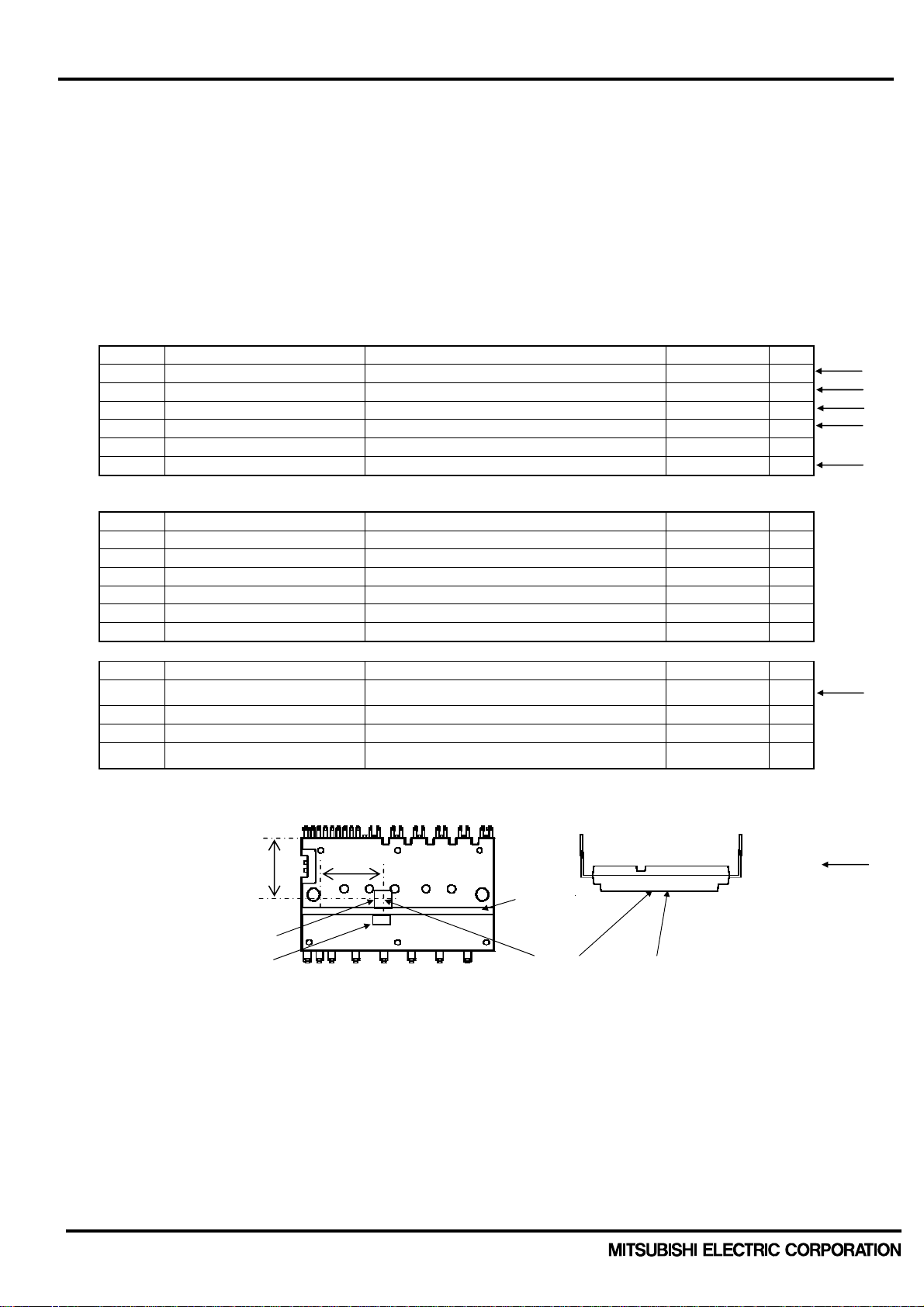
The maximum ratings of PSS10S72FT are shown in Table 2-1-1.
Table 2-1-1 Maximum Ratings
INVERTER PART
Symbol Parameter Condition Ratings Unit
V
CC
V
CC(surge)
V
CES
±IC Each IGBT collector current
±ICP Each IGBT collector current (peak) TC= 25°C, less than 1ms 20 A
Tj Junction temperature -30~+150
Note: Pulse width and period are limited due to junction temperature.
CONTROL (PROTECTION) PART
Symbol Parameter Condition Ratings Unit
VD Control supply voltage Applied between VP1-VNC, VN1-VNC 20 V
VDB Control supply voltage Applied between V
VIN Input voltage Applied between UP, VP, WP-VNC, UN, VN, WN-VNC -0.5~VD+0.5 V
VFO Fault output supply voltage Applied between FO-VNC -0.5~VD+0.5 V
IFO Fault output current Sink current at FO terminal 1 mA
VSC Current sensing input voltage Applied between CIN-VNC -0.5~VD+0.5 V
TOTAL SYSTEM
Symbol Parameter Condition Ratings Unit
V
CC(PROT)
TC Module case operation temperature Measurement point of Tc is described below -30~+100 °C
T
Storage temperature -40~+125 °C
stg
V
Isolation voltage
iso
Supply voltage Applied between P-NU,NV,NW 900
Supply voltage (surge) Applied between P-NU,NV,NW 1000
Collector-emitter voltage 1200
10
800
2500 V
Self protection supply voltage limit
(Short circuit protection capability)
TC= 25°C (Note)
, V
UFB-VUFS
= 13.5~16.5V, Inverter Part
V
D
= 125°C, non-repetitive, less than 2μs
T
60Hz, Sinusoidal, AC 1min, between connected all pins
and heat sink plate
VFB-VVFS
,V
WFB-VWFS
20 V
Tc measurement position
Control terminals
18mm
IGBT chip position
FWDi chip position
(1) Vcc The maximum voltage can be biased between P-N. A voltage suppressing circuit such as a brake circuit is
necessary if P-N voltage exceeds this value.
(2) Vcc(surge) The maximum P-N surge voltage in switching state. If P-N voltage exceeds this voltage, a snubber circuit is
necessary to absorb the surge under this voltage.
(3) V
(4) +/-I
The maximum sustained collector-emitter voltage of built-in IGBT and FWDi.
CES
The allowable continuous current flowing at collect electrode (Tc=25°C) Pulse width and period are limited due to
C
junction temperature.
(5) Tj The maximum junction temperature rating is 150°C.But for safe operation, it is recommended to limit the average
junction temperature up to 125°C. Repetitive temperature variation ∆Tj affects the life time of power cycle, so refer
life time curves for safety design.
(6) Vcc(prot) The maximum supply voltage for turning off IGBT safely in the case of an SC or OC faults. The power chip might not
be protected and break down in the case that the supply voltage is higher than this specification.
18mm
Power terminals
Groove
Tc point
Heat sink side
V
V
V
A
°C
V
(1)
(2)
(3)
(4)
(5)
rms
(6)
(7)
Publication Date: September 2015
5
Page 6
<Dual-In-Line Package Intelligent Power Module>
1200V Mini DIPIPM with BSD Series APPLICATION NOTE
(7) Tc position Tc (case temperature) is defined to be the temperature just beneath the specified power chip. Please mount a
thermocouple on the heat sink surface at the defined position to get accurate temperature information. Due to the
control schemes such different control between P and N-side, there is the possibility that highest Tc point is different
from above point. In such cases, it is necessary to change the measuring point to that under the highest power chip.
[Power chip position]
Fig.2-1-1 indicate the position of the each power chips. (This figure is the view from laser marked side.)
Dimension in mm
IGBT
FWDi
WN VN UN WP VP UP
Fig.2-1-1 Power chip position
Publication Date: September 2015
6
Page 7
<Dual-In-Line Package Intelligent Power Module>
1200V Mini DIPIPM with BSD Series APPLICATION NOTE
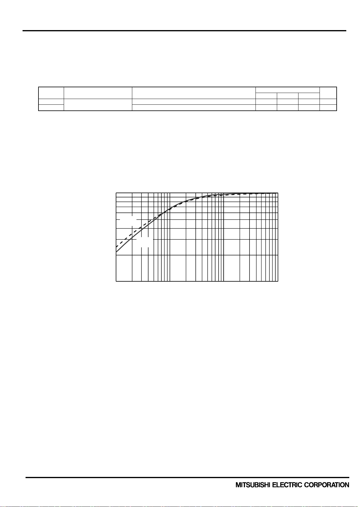
2.1.2 Thermal Resistance
Table 2-1-2 shows the thermal resistance of PSS10S72FT.
Table 2-1-2 Thermal resistance of PSS10S72FT
THERMAL RESISTANCE
Symbol Parameter Condition
R
th(j-c)Q
R
th(j-c)F
Note : Grease with good thermal conductivity and long-term endurance should be applied evenly with about +100μm~+200μm on the contacting surface of
Junction to case thermal
resistance (Note)
Inverter FWDi part (per 1/6 module) - - 1.8 K/W
DIPIPM and heat sink. The contacting thermal resistance between DIPIPM case and heat sink Rth(c-f) is determined by the thickness and the thermal
conductivity of the applied grease. For reference, Rth(c-f) is about 0.3K/W (per 1/6 module, grease thickness: 20μm, thermal conductivity: 1.0W/m•k).
Inverter IGBT part (per 1/6 module) - - 1.5 K/W
The above data shows the thermal resistance between chip junction and case at steady state. The thermal
resistance goes into saturation in about 10 seconds. The unsaturated thermal resistance is called as
transient thermal impedance which is shown in Fig.2-1-3. Zth(j-c)* is the normalized value of the transient
thermal impedance. (Zth(j-c)*= Zth(j-c) / Rth(j-c)max)
For example, the IGBT transient thermal impedance of PSS10S72FT in 0.2s is 1.61×0.8=1.288
The transient thermal impedance isn’t used for constantly current, but for short period current (ms order).
(e.g. in the cases at motor starting, at motor lock・・・)
Limits
Min. Typ. Max.
K/W.
Unit
1.0
FWDi
IGBT
0.1
Normalized thermal impedance Zth(j-c)
0.01 0.1 1 10
Time(s)
Fig.2-1-3 Typical transient thermal impedance (PSSxxS72FT)
Publication Date: September 2015
7
Page 8

<Dual-In-Line Package Intelligent Power Module>
1200V Mini DIPIPM with BSD Series APPLICATION NOTE
2.1.3 Electric Characteristics and Recommended Conditions
Table 2-1-3 shows the typical static characteristics and switching characteristics of PSS10S72FT.
Table 2-1-3 Static characteristics and switching characteristics of PSS10S72FT.
INVERTER PART (T
Symbol Parameter Condition
V
CE(sat)
Collector-emitter saturation
voltage
VEC FWDi forward voltage VIN= 0V, -IC= 10A - 1.90 2.40 V
ton
t
- 0.45 0.90 μs
C(on)
t
- 2.40 3.40 μs
off
t
C(off)
Switching times
- 0.40 0.80 μs
trr - 0.50 - μs
I
CES
Collector-emitter cut-off
current
Switching time definition and performance test method are shown in Fig.2-1-4 and 2-1-5.
Switching characteristics are measured by half bridge circuit with inductance load.
90%
10% 10% 10% 10%
tc(on)
V
CIN
td(on)
( ton=td(on)+tr ) ( toff=td(off)+tf )
Fig.2-1-4 Switching time definition Fig.2-1-5 Evaluation circuit (inductive load)
Short A for N-side IGBT, and short B for P-side IGBT evaluation
Turn on
= 25°C, unless otherwise noted)
j
trr
Ic
Irr
tc(off)
tr
td(off) tf
= 15V, VIN= 5V, IC= 10A
V
D=VDB
= 600V, VD= VDB= 15V
V
CC
= 10A, Tj= 125°C, VIN= 0↔5V
I
C
Inductive Load (upper-lower arm)
CE=VCES
90%
V
CE
P-side SW
Input signal
V
VIN(5V0V)
V
N-side SW
Input signal
t:200ns/div
Min. Typ. Max.
T
= 25°C - 1.50 2.20
j
Tj= 125°C - 1.75 2.50
1.10 1.80 2.50 μs
T
= 25°C - - 1
j
Tj= 125°C - - 10
V
UFB,VVFB,VWFB
V
P1
V
UP,VP,W
D
UN,VN,W
CC
P
IN
COM
V
N1
V
CC
N
IN
V
NC
GND CIN
V
B
HO
V
S
LO
CIN
P
U,V,W
NU,NV,
NW
Turn off
Limits
VDB
V
UFS,VVFS,VWFS
L load
N-side
P-side
L load
t:200ns/div
Unit
V
mA
V
CC
Ic
Conditions: VCC=600V, VD=VDB=15V, Tj=125°C, Ic=10A, Inductive load half-bridge circuit
Publication Date: September 2015
Ic(5A/div)
VCE(200V/div)
PSS10S72FT (10A/1200V)
Fig.2-1-6 Typical switching waveform
8
V
(200V/div)
CE
Ic(5A/div)
Page 9

<Dual-In-Line Package Intelligent Power Module>
)
1200V Mini DIPIPM with BSD Series APPLICATION NOTE
Table 2-1-4 shows the typical control part characteristics of PSS20S71F6.
Table 2-1-4 Control (Protection) characteristics of PSS20S71F6
CONTROL (PROTECTION) PART (T
Symbol Parameter Condition
ID
Circuit current
IDB
V
Short circuit trip level VD = 15V
SC(ref)
UV
DBt
P-side Control supply
UV
UVDt
UVDr Reset level 10.8 - 13.0 V
under-voltage protection(UV)
Reset level 10.5 - 12.5 V
DBr
N-side Control supply
under-voltage protection(UV)
VOT Temperature output Pull down R=5kΩ (Note 2)
V
FOH
V
FOL
Fault output voltage
V
tFO Fault output pulse width CFO=22nF
IIN Input current VIN = 5V 0.70 1.00 1.50 mA
V
ON threshold voltage
th(on)
V
OFF threshold voltage 0.8 - -
th(off
VF Bootstrap Di forward voltage
R
Note 1 : SC protection works only for N-side IGBT. Please select the external shunt resistance such that the SC trip-level is less than 2 times of the current rating.
Note 2 : DIPIPM don't shutdown IGBTs and output fault signal automatically when temperature rises excessively. When temperature exceeds the protective level that
Built-in limiting resistance
user defined, controller (MCU) should stop the DIPIPM.
3 : Fault signal Fo outputs when SC or UV protection works. Fo pulse width is different for each protection modes. At SC failure, Fo pulse width is a fixed width
which is specified by the capacitor connected to C
state. (But minimum Fo pulse width is the specified time by C
Recommended operating conditions of PSS10S72FT are given in Table 2-1-5. It is highly recommended to
operate the modules within these conditions so as to ensure DIPIPM safe operation.
Table 2-1-5 Recommended operating conditions of PSS10S72FT
RECOMMENDED OPERATION CONDITIONS
Symbol Parameter Condition
VCC Supply voltage Applied between P-NU, NV, NW
VD Control supply voltage Applied between VP1-VNC, VN1-VNC
VDB Control supply voltage Applied between V
∆VD, ∆VDB Control supply variation
t
Arm shoot-through blocking time For each input signal
dead
f
PWM input frequency TC ≤ 100°C, Tj ≤ 125°C
PWM
IO Allowable r.m.s. current
PWIN(on)
PWIN(off)
VNC V
Tj Junction temperature
Note 1: Allowable r.m.s. current depends on the actual application conditions.
2: DIPIPM might not make response if the input signal pulse width is less than PWIN(on)
3: IPM might make delayed response or no response for the input signal with off pulse width less than PWIN(off). Please refer below about delayed response.
Delayed Response Against Shorter Input Off Signal Than PWIN(off) (P-side only)
Minimum input pulse width
variation Between VNC-NU, NV, NW (including surge)
NC
= 25°C, unless otherwise noted)
j
Tota l o f VP1-VNC, VN1-VNC
Each part of V
- V
V
VFB
VFS
, V
WFB
UFB
- V
- V
WFS
UFS
,
Limits
Min. Typ. Max.
V
=15V, VIN=0V - - 6.00
D
VD=15V, VIN=5V - - 6.00
V
=15V, VIN=0V - - 0.55
D=VDB
VD=VDB=15V, VIN=5V - - 0.55
(Note 1)
0.45 0.48 0.51 V
Unit
mA
Trip level 10.0 - 12.0 V
≤125°C
T
j
Trip level 10.3 - 12.5 V
LVIC Temperature=85C
2.51 2.64 2.76 V
VSC = 0V, FO terminal pulled up to 5V by 10kΩ 4.9 - - V
= 1V, IFO = 1mA - - 0.95 V
SC
Applied between U
IF=10mA including voltage drop by limiting resistor
, VP, WP, UN, VN, WN-VNC
P
(Note 3)
1.6 2.4 - ms
- - 3.5
0.5 0.9 1.3 V
V
Included in bootstrap Di 16 20 24 Ω
terminal. (C
FO
=9.1 x 10⁻⁶ x tFO [F]), but at UV failure, Fo outputs continuously until recovering from UV
FO
.)
FO
, V
UFB-VUFS
V
= 600V, VD = 15V, P.F = 0.8,
CC
Sinusoidal PWM
≤ 100°C, Tj ≤ 125°C (Note1)
T
C
V
200V
13.5VV
13.0VV
-20CTc 100C,
N-line wiring inductance
less than 10nH
350V,
CC
16.5V,
D
18.5V,
DB
Below rated current
Between rated current
and 1.7 times of rated
current
(Note 3)
VFB-VVFS
, V
WFB-VWFS
f
PWM
f
PWM
= 5kHz
= 15kHz
(Note 2)
Limits
Min. Typ. Max.
350 600 800
13.5 15.0 16.5
13.0 15.0 18.5
-1 - +1
3.0 - -
- - 20
- - 5.3
- - 3.6
2.0 - -
2.5 - -
2.9 - -
-5.0 - +5.0
-20 - +125
Unit
V
V
V
V/μs
μs
kHz
Arms
μs
V
°C
Publication Date: September 2015
9
Page 10
<Dual-In-Line Package Intelligent Power Module>
1200V Mini DIPIPM with BSD Series APPLICATION NOTE
P Side Control Input
Internal IGBT Gate
Output Current Ic
Real line: off pulse width > PWIN(off); turn on time t1
Broken line: off pulse width < PWIN(off); turn on time t2
(t1:Normal switching time)
About Control supply variation
If high frequency noise superimposed to the control supply line, IC malfunction might happen and cause DIPIPM erroneous
operation. To avoid such problem, line ripple voltage should meet the following specifications:
dV/dt +/-1V/μs, Vripple2Vp-p
2.1.4 Mechanical Characteristics and Ratings
The mechanical characteristics and ratings are shown in Table 2-1-6.
Please refer to Section 2.4 for the detailed mounting instruction of Mini DIPIPM.
Table 2-1-6 Mechanical characteristics and ratings of PSS10S72FT
MECHANICAL CHARACTERISTICS AND RATINGS
Parameter Condition
Mounting torque Mounting screw : M3 (Note 1) Recommended 0.78 N·m 0.59 - 0.98 N·m
Terminal pulling strength Load 9.8N EIAJ-ED-4701 10 - - s
Terminal bending strength
Weight - 21 - g
Heat-sink flatness
Note 1: Plain washers (ISO 7089~7094) are recommended.
Note 2: Measurement point of heat sink flatness
Load 4.9N
90deg. bend
-
+
Measurement position
Heat sink side
t2
t1
Limits
Min. Typ. Max.
EIAJ-ED-4701 2 - - times
(Note 2)
-50 - 100 μm
12.78mm
4.65mm
13.5mm
23mm
+
-
Heat sink side
Unit
Publication Date: September 2015
10
Page 11
<Dual-In-Line Package Intelligent Power Module>
1200V Mini DIPIPM with BSD Series APPLICATION NOTE
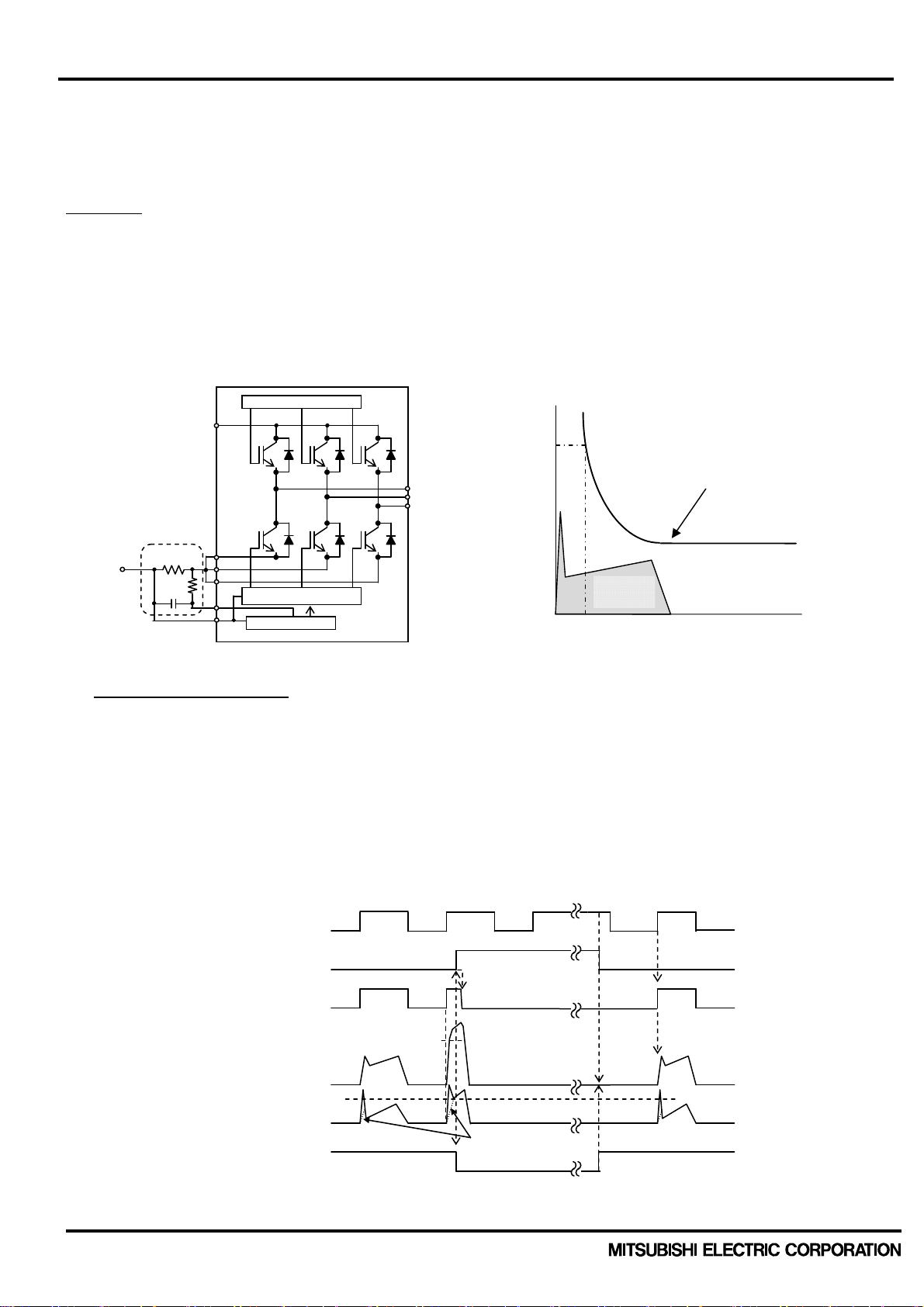
2.2 Protective Functions and Operating Sequence
Mini DIPIPM has Short circuit (SC), Under Voltage of control supply (UV) and temperature output (VOT) for
protection function. The operating principle and sequence are described below.
2.2.1 Short Circuit Protection
1. General
Mini DIPIPM uses external shunt resistor for the current detection as shown in Fig.2-2-1. The internal
protection circuit inside the IC captures the excessive large current by comparing the CIN voltage generated at
the shunt resistor with the referenced SC trip voltage, and perform protection automatically. The threshold
voltage trip level of the SC protection Vsc(ref) is typ. 0.48V.
In case of SC protection happens, all the gates of N-side three phase IGBTs will be interrupted together with
a fault signal output. To prevent DIPIPM erroneous protection due to normal switching noise and/or recovery
current, it is necessary to set an RC filter (time constant: 1.5μ ~ 2μs) to the CIN terminal input (Fig.2-2-1, 2-2-2).
Also, please make the pattern wiring around the shunt resistor as short as possible.
SC protection external
Shunt resistor
N1
P
P-side IGBTs
N-side IGBTs
NU
NV
R
NW
C
CIN
V
NC
Fig.2-2-1 SC protecting circuit Fig.2-2-2 Filter time constant setting
Drive Circuit
U
V
W
Drive Circuit
SC Protection
SC protective level
Collect current Ic
Collector
current
0
2
Input pulse width tw (μs)
2. SC protection Sequence
SC protection (N-side only with the external shunt resistor and RC filter)
a1. Normal operation: IGBT ON and carrying current.
a2. Short circuit current detection (SC trigger).
It is necessary to set RC time constant so that IGBT shut down within 2.0μs when SC. (1.5~2.0μs is recommended generally.)
a3. All N-side IGBTs’ gate are hard interrupted.
a4. All N-side IGBTs turn OFF.
a5. Fo outputs.
The pulse width of the Fo signal is set by the external capacitor CFO.
a6. Input = “L”. IGBT OFF
a7. Fo finishes output, but IGBTs don't turn on until inputting next ON signal (LH).
IGBT of each phase can return to normal state by inputting ON signal to each phase.
a8. Normal operation: IGBT ON and outputs current.
Lower-side control
input
Protection circuit state
Internal IGBT gate
Output current Ic
Sense voltage of
the shunt resistor
Error output Fo
SC trip current level
a1
SET
a3
a4
a2
SC reference voltage
a5
a6
Delay by RC filtering
Fig.2-2-3 SC protection timing chart
Publication Date: September 2015
RESET
a8
a7
11
Page 12

<Dual-In-Line Package Intelligent Power Module>
1200V Mini DIPIPM with BSD Series APPLICATION NOTE
3. Determination of Shunt Resistance
(1) Shunt resistance
The value of current sensing resistance is calculated by the following formula:
= V
R
Shunt
where V
is the SC trip voltage.
SC(ref)
The maximum SC trip level SC(max) should be set less than the IGBT minimum saturation current which is
1.7 times as large as the rated current. For example, the SC(max) of PSS10S72FT should be set to
10x1.7=17A. The parameters (V
SC(ref)
level.
For example of PSS10S72FT, there is +/-0.03V dispersion in the spec of V
Table 2-2-1 Specification for V
SC(ref)
Condition Min Typ Max
at Tj=25°C, VD=15V
Then, the range of SC trip level can be calculated by the following expressions:
R
Shunt(min)=VSC(ref) max
R
Shunt(typ)
R
Shunt(max)
So the SC trip level range is described as Table 2-2-2.
*)This is the case that shunt resistance dispersion is within +/-5%.
= R
= R
Shunt(min)
Shunt(typ)
Table 2-2-2 Operative SC Range (R
Condition min. typ. Max.
at Tj=25°C, V
(e.g. 30mΩ (R
=15V
D
shunt(min)
)= 0.51V (=V
There is the possibility that the actual SC protection level becomes less than the calculated value. This is
considered due to the resonant signals caused mainly by parasitic inductance and parasitic capacity. It is
recommended to make a confirmation of the resistance by prototype experiment.
(2) RC Filter Time Constant
It is necessary to set an RC filter in the SC sensing circuit in order to prevent malfunction of SC protection
due to noise interference. The RC time constant is determined depending on the applying time of noise
interference and the SCSOA of the DIPIPM.
When the voltage drop on the external shunt resistor exceeds the SC trip level, The time (t1) that the CIN
terminal voltage rises to the referenced SC trip level can be calculated by the following expression:
IRV
cshuntSC
V
t
Vsc : the CIN terminal input voltage, Ic : the peak current, τ : the RC time constant
SC
IR
On the other hand, the typical time delay t2 (from Vsc voltage reaches Vsc(ref) to IGBT gate shutdown) of
IC is shown in Table 2-2-3.
Table 2-2-3 Internal time delay of IC
Item Min typ max Unit
IC transfer delay time -
Therefore, the total delay time from an SC level current happened to the IGBT gate shutdown becomes:
=t1+t2
t
TOTAL
/SC
SC(ref)
, R
) dispersion should be considered when designing the SC trip
Shunt
as shown in Table 2-2-1.
SC(ref)
(unit: V)
0.45 0.48 0.51
/SC(max)
/ 0.95* then SC(typ) = V
x 1.05* then SC(min)= V
=30mΩ (min), 31.6mΩ (typ), 33.2mΩ(max)
Shunt
SC(ref) typ
SC(ref) min
/ R
/ R
Shunt(typ)
Shunt(max)
13.5A 15.2A 17A
) / 17A(=SC(max))
SC(max)
1
t
)1(
)1ln(1
cshunt
- 1.0
μs
Publication Date: September 2015
12
Page 13

<Dual-In-Line Package Intelligent Power Module>
1200V Mini DIPIPM with BSD Series APPLICATION NOTE
DBt
(P)
In this voltage range, built-in control IC may not work properly.
Normal operating of each protection function (UV, Fo output etc.) is
not also assured.
Normally IGBT does not work. But external noise may cause DIPIPM
malfunction (turns ON), so DC-link voltage need to start up after
control supply starts-up.
UV function becomes active and output Fo (N-side only).
Even if control signals are applied, IGBT does not work
IGBT can work. However, conducting loss and switching loss will
increase, and result extra temperature rise at this state,.
Recommended conditions.
IGBT works. However, switching speed becomes fast and saturation
current becomes large at this state, increasing SC broken risk.
The control circuit might be destroyed.
+/-1V/μs, Vripple2Vp-p
dV/dt
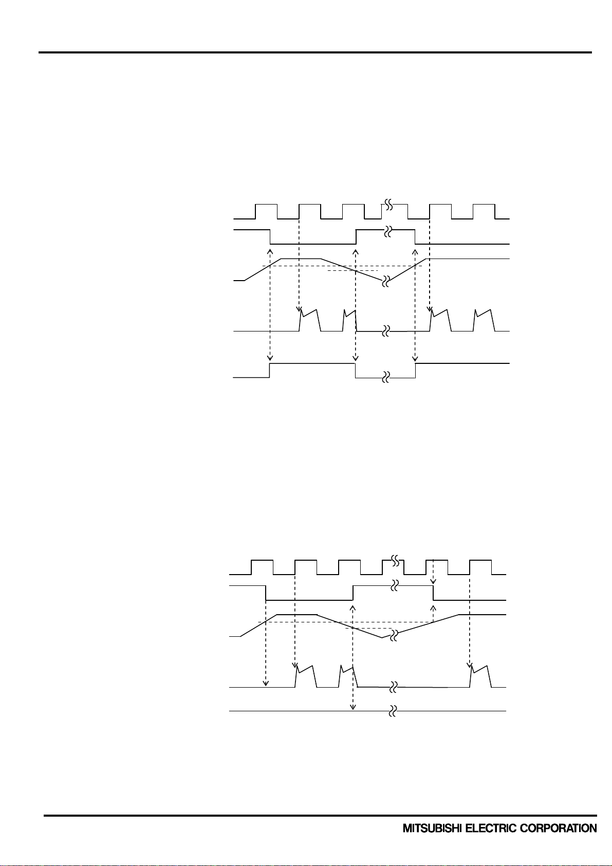
2.2.2 Control Supply UV Protection
The UV protection is designed to prevent unexpected operating behavior as described in Table 2-2-4.
Both P-side and N-side have UV protecting function. However, fault signal (Fo) output only corresponds to
N-side UV protection. Fo output continuously during UV state.
In addition, there is a noise filter (typ. 10μs) integrated in the UV protection circuit to prevent instantaneous
UV erroneous trip. Therefore, the control signals are still transferred in the initial 10μs after UV happened.
Table 2-2-4 DIPIPM operating behavior versus control supply voltage
Control supply voltage Operating behavior
0-4.0V (P, N)
4.0-UVDt (N), UV
UVDt (N)-13.5V
UV
(P)-13.0V
DBt
13.5-16.5V (N)
-18.5V (P)
13.0
16.5-20.0V (N)
-20.0V (P)
18.5
20.0V- (P, N)
Ripple Voltage Limitation of Control Supply
If high frequency noise superimposed to the control supply line, IC malfunction might happen and
cause DIPIPM erroneous operation. To avoid such problem happens, line ripple voltage should meet the
following specifications:
Publication Date: September 2015
13
Page 14
<Dual-In-Line Package Intelligent Power Module>
1200V Mini DIPIPM with BSD Series APPLICATION NOTE
[N-side UV Protection Sequence]
a1. Control supply voltage V
ON signal (LH).
(IGBT of each phase can return to normal state by inputting ON signal to each phase.)
a2. Normal operation: IGBT ON and carrying current.
a3. V
level dips to under voltage trip level. (UVDt).
D
a4. All N-side IGBTs turn OFF in spite of control input condition.
a5. Fo outputs for the period set by the capacitance C
a6. V
level reaches UVDr.
D
a7. Normal operation: IGBT ON and outputs current.
Control input
Protection circuit state
Control supply voltage V
Output current Ic
Error output Fo
[P-side UV Protection Sequence]
a1. Control supply voltage V
IGBT turns on by next ON signal (LH).
a2. Normal operation: IGBT ON and outputs current.
a3. V
level drops to under voltage trip level (UV
DB
a4. IGBT of the corresponding phase only turns OFF in spite of control input signal level,
but there is no F
a5. V
level reaches UV
DB
signal output.
O
a6. Normal operation: IGBT ON and outputs current.
Control input
Protection circuit state
Control supply voltage V
Output current Ic
Error output Fo
exceeds under voltage reset level (UVDr), but IGBT turns ON by next
D
but output is extended during VD keeps below UVDr.
FO,
RESET
SET
RESET
UVDr
D
a1
UV
Dt
a3
a6
a2
a4
a7
a5
Fig.2-2-4 Timing chart of N-side UV protection
rises. After the voltage reaches under voltage reset level UV
DB
).
DBt
.
DBr
RESET SET
UV
DBr
DB
a1
UV
a2
a3
DBt
a4
Keep High-level (no fault output)
RESET
a5
a6
Fig.2-2-5 Timing Chart of P-side UV protection
DBr
,
Publication Date: September 2015
14
Page 15
<Dual-In-Line Package Intelligent Power Module>
g
g
1200V Mini DIPIPM with BSD Series APPLICATION NOTE
2.2.3 Temperature output function V
(1) Usage of this function
This function measures the temperature of control LVIC by built in temperature sensor on LVIC.
The heat generated at IGBT and FWDi transfers to LVIC through molding resin of package and outer heat sink.
So LVIC temperature cannot respond to rapid temperature rise of those power chips effectively. (e.g. motor
lock, short circuit) It is recommended to use this function for protecting from slow excessive temperature rise
by such cooling system down and continuance of overload operation. (Replacement from the thermistor
which was mounted on outer heat sink currently)
[Note]
In this function, DIPIPM cannot shutdown IGBT and output fault signal by itself when temperature rises
excessively. When temperature exceeds the defined protection level, controller (MCU) should stop the DIPIPM.
←LVIC
(Detecting point)
Power Chip Area
Fig.2-2-6 Temperature detecting point Fig.2-2-7 Thermal conducting from power chips
(2) VOT characteristics
output circuit, which is described in Fig.2-2-9, is the output of OP amplifier circuit. The current capability
V
OT
output is described as Table 2-2-6. The characteristics of VOT output vs. LVIC temperature is linear
of V
OT
characteristics described in Fig.2-2-13. There are some cautions for using this function as below.
Table 2-2-6 Output capability
(Tc=-20°C ~100°C)
min.
Source 1.7mA
Sink 0.1mA
Source: Current flow from V
Sink : Current flow from outside to V
OT
In the case of detecting lower temperature than room temperature
It is recommended to insert 5.1kΩ pull down resistor for getting linear output characteristics at lower
temperature than room temperature. When the pull down resistor is inserted between V
GND), the extra current calculated by V
continuously. In the case of only using V
necessary to insert the pull down resistor.
Temperature
nal
si
Fig.2-2-9 VOT output circuit in the case of detecting low temperature
OT
to outside.
.
OT
FWDi
IGBT
LVI C
Heatsink
Temperature of
LIVC is affected
from heatsink.
Inside LVIC
of DIPIPM
Temperature
V
nal
si
Ref
OT
VNC
Fig.2-2-8 VOT output circuit
and VNC(control
OT
output voltage / pull down resistance flows as LVIC circuit current
OT
for detecting higher temperature than room temperature, it isn't
OT
Inside LVIC
of DIPIPM
V
OT
Ref
VNC
MCU
5.1kΩ
MCU
5V
Publication Date: September 2015
15
Page 16
<Dual-In-Line Package Intelligent Power Module>
g
1200V Mini DIPIPM with BSD Series APPLICATION NOTE
In the case of using with low voltage controller(MCU)
In the case of using V
voltage 3.3V when temperature rises excessively. If system uses low voltage controller, it is recommended to
insert a clamp Di between control supply of the controller and this output for preventing over voltage.
Fig.2-2-10 VOT output circuit in the case of using with low voltage controller
In the case that the protection level exceeds control supply of the controller
In the case of using low voltage controller like 3.3V MCU, if it is necessary to set the trip V
supply voltage (e.g. 3.3V) or more, there is the method of dividing the V
circuit and then inputting to A/D converter on MCU (Fig.2-2-11). In that case, sum of the resistances of divider
circuit should be almost 5.1kΩ. About the necessity of clamp diode, we consider that the divided output will not
exceed the supply voltage of controller generally, so it will be unnecessary to insert the clump diode. But it
should be judged by the divided output level finally.
Temperature
nal
si
with low voltage controller (e.g. 3.3V MCU), VOT output might exceed control supply
OT
Inside LVIC
of DIPIPM
Temperature
signal
Ref
V
OT
VNC
MCU
level to control
OT
output by resistance voltage divider
OT
Inside LVIC
of DIPIPM
Ref
Fig.2-2-11 V
VOT
VNC
DVOT=V
output circuit in the case with high protection level
OT
R1
DV
OT
R2
·R2/(R1+R2) R1+R2≈5.1kΩ
OT
MCU
Publication Date: September 2015
16
Page 17

<Dual-In-Line Package Intelligent Power Module>
1200V Mini DIPIPM with BSD Series APPLICATION NOTE
4.0
3.8
3.6
3.4
3.2
3.0
2.8
2.76
2.64
2.6
2.51
2.4
2.2
2.0
1.8
VOT output (V)_
1.6
1.4
1.2
1.0
0.8
Outputrangewithout5kΩpulldownresistor
(Outputmightbesaturatedunderthislevel.)
0.6
0.4
0.2
0.0
-30 -20 -10 0 10 20 30 40 50 60 70 80 90 100 110 120 130
Typ.Max. Min .
(3) Usage of V
function
OT
As mentioned above, the heat of power chips transfers to LVIC through the heat sink and package, so the
relationship between LVIC temperature: Tic(=V
datasheet), and junction temperature: Tj depends on the system cooling condition, heat sink, control strategy,
etc. For example of PSSxxS72FT, their relationship example in the case of using the heat sink (Table 2-2-7) is
described in Fig.2-2-13. This relationship may be different due to the cooling conditions. So when setting the
threshold temperature for protection, it is necessary to get the relationship between them on your real system.
And when setting threshold temperature Tic, it is important to consider the protection temperature keeps
Tj 150°C.
Outputrangewith5kΩpulldownresistor
(Outputmightbesaturatedunderthisleve l.)
LVIC temperature (°C)
Fig.2-2-12 V
output vs. LVIC temperature
OT
output), case temperature: Tc(under the chip defined on
OT
Publication Date: September 2015
17
Page 18

<Dual-In-Line Package Intelligent Power Module>
1200V Mini DIPIPM with BSD Series APPLICATION NOTE
Table 2-2-7 Outer heat sink
Heat sink size
( W x D x H )
200 x 85 x 40 mm
140
120
W
D
H
100
Temperature[°C]
Tj
80
Tc
Tic
60
40
20
0
10 15 20 25 30 35 40 45 50 55 60
Loss [W]
Fig.2-2-13 Example of relationship of Tj, Tc, Tic
(
One IGBT chip turns on. DC current Ta=25°C)
Procedure about setting the protection level by using Fig.2-2-14 is described as below.
Table 2-2-8 Procedure for setting protection level
Procedure Setting value example
1) Set the protection Tj temperature Set Tj to 135°C as protection level.
Get LVIC temperature Tic that matches to above Tj
2)
of the protection level from the relationship of Tj-Tic
Tic=85°C (@Tj=135°C)
in Fig.2-2-14.
Get V
Fig.2-2-15 and the Tic value which was obtained at
3)
phase 2) .
value from the VOT output characteristics in
OT
V
=2.64V (@Tic=85°C) is decided as the
OT
protection level.
As above procedure, the setting value for V
output is decided to 2.64V. But VOT output has some data
OT
spread, so it is important to confirm whether the protection temperature fluctuation of Tj is not Tj>150°C due
to the data spread of V
output. Procedure about the confirmation of temperature fluctuation is described in
OT
Table 2-2-9.
Table 2-2-9 Procedure for confirmation of temperature fluctuation
Procedure Confirmation example
Confirm the region of Tic fluctuation at above V
4)
from Fig.2-2-15.
Confirm the region of Tj fluctuation at above region
5)
of Tic from Fig.2-2-14.
OT
Tic=80°C~90°C (@VOT=2.64V)
Tj=117°C~147°C (≤150°C No problem)
In this case, fluctuation of Tc is
Tc=100°C~120°C
Publication Date: September 2015
18
Page 19

<Dual-In-Line Package Intelligent Power Module>
1200V Mini DIPIPM with BSD Series APPLICATION NOTE
150
140
1) 135℃
5) Tj: 117℃ ~147℃
Tj
130
120
5) Tc: 100℃ ~120℃
Tc
110
100
90
80
4) 90℃
2) 85℃
4) 80℃
Tic
70
60
50
30 35 40 45 50 55 60
3.2
Loss [W]
Temperature[°C]
Fig.2-2-14 Relationship of Tj, Tc, Tic(Enlarged graph of Fig.2-2-13)
Max
3.0
Typ.
2.8
3) 2.64V
2.6
2.4
VOT output (V)_
2.2
2.0
1.8
70 80 90 100
Fig.2-2-15 V
4)80℃
2) 85℃
LVIC temperature ( °C)
output vs. LVIC temperature (Enlarged graph of Fig.2-2-12)
OT
4) 90℃
Min.
The relationship between Tic, Tc(measuring) and Tj(calculated by loss) depends on the system
cooling condition and control strategy, and so on. So please evaluate about these temperature
relationship on your real system when considering the protection level.
If necessary, it is possible to ship the sample with the individual data of V
vs. LVIC temperature.
OT
Publication Date: September 2015
19
Page 20

<Dual-In-Line Package Intelligent Power Module>
1200V Mini DIPIPM with BSD Series APPLICATION NOTE
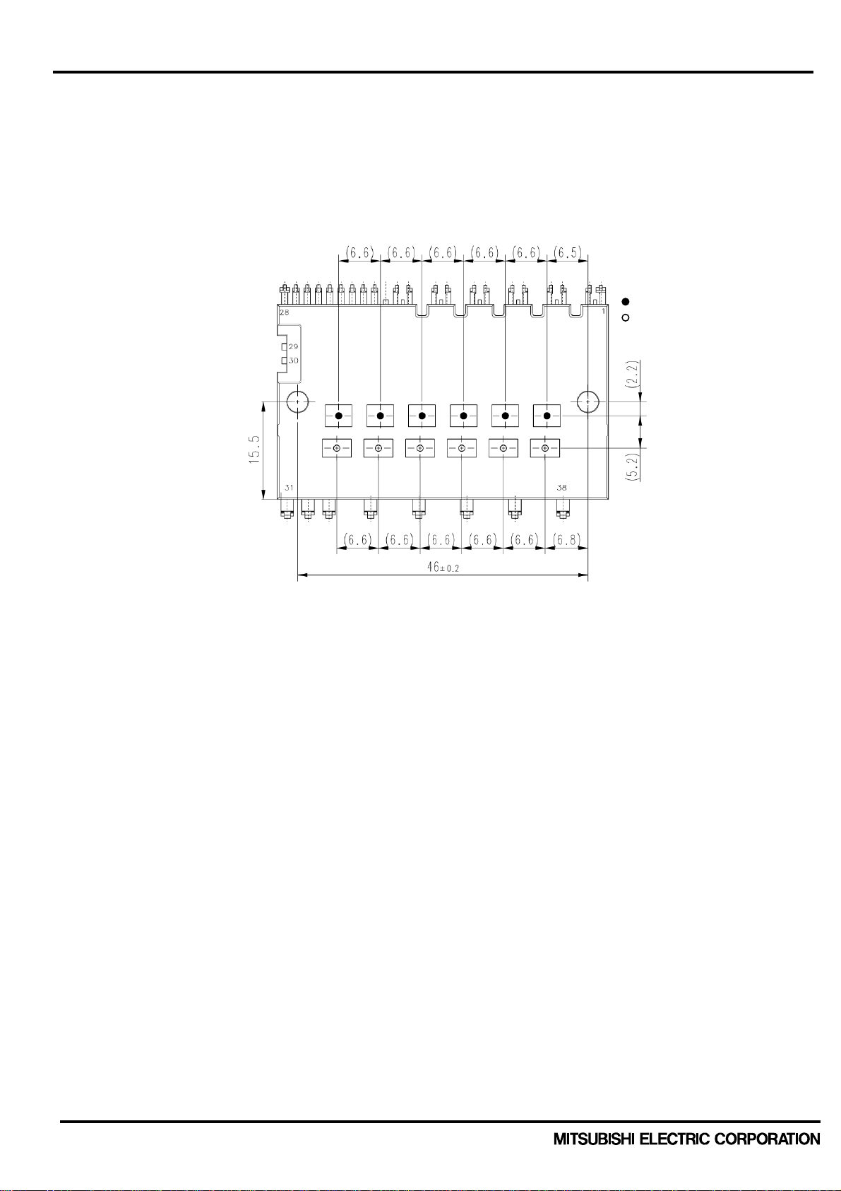
2.3 Package Outlines
2.3.1 Package outlines
Fig.2-3-1 PSSxxS72FT package outline drawing (Dimension in mm)
Publication Date: September 2015
QR Code is registered trademark of DENSO WAVE INCORPORATED in JAPAN and other countries.
20
Page 21

<Dual-In-Line Package Intelligent Power Module>
1200V Mini DIPIPM with BSD Series APPLICATION NOTE
2.3.2 Marking
The laser marking specifications of Mini DIPIPM is described in Fig.2-3-2. Mitsubishi Corporate crest, Type
name, Lot number, and QR code mark are marked in the upper side of module.
PSS**S72FT
Lot number
“JAPAN” mark is printed for JAPAN product only.
QR Code is registered trademark of DENSO WAVE INCORPORATED
in JAPAN and other countries.
Fig.2-3-2 Laser marking view PSSxxS72FT (Dimension in mm)
The Lot number indicates production year, month, running number and country of origin.
The detailed is described as below.
(Example)
C 3 9 AA1
Running number
Product month (however O: October, N: November, D: December)
Last figure of Product year (e.g. 2013
)
Factory identification
None : Manufactured at the factory in Japan
C : Manufactured at the factory A in China
H : Manufactured at the factory B in China
Publication Date: September 2015
21
Page 22

<Dual-In-Line Package Intelligent Power Module>
1200V Mini DIPIPM with BSD Series APPLICATION NOTE
2.3.3 Terminal Description
Table 2-3-1 Terminal description (PSSxxS72FT)
No. Symbol Description
1 V
2 (UPG) Dummy-pin
3 V
4 VP1 U-phase P-side control supply positive terminal
5 (COM) Dummy-pin
6 UP U-phase P-side control input terminal
7 V
8 (VPG) Dummy-pin
9 V
10 VP1 V-phase P-side control supply positive terminal
11 (COM) Dummy-pin
12 VP V-phase P-side control input terminal
13 V
14 (WPG) Dummy-pin
15 V
16 VP1 W-phase P-side control supply positive terminal
17 COM Dummy-pin
18 WP W-phase P-side control input terminal
19 (UNG) Dummy-pin
20 VOT Temperature output
21 UN U-phase N-side control input terminal
22 VN V-phase N-side control input terminal
23 WN W-phase N-side control input terminal
24 FO Fault signal output terminal
25 CFO Fault pulse output width setting terminal
26 CIN SC current trip voltage detecting terminal
27 VNC N-side control supply GND terminal
28 VN1 N-side control supply positive terminal
29 (WNG) Dummy-pin
30 (VNG) Dummy-pin
31 NW WN-phase IGBT emitter
32 NV VN-phase IGBT emitter
33 NU UN-phase IGBT emitter
34 W W-phase output terminal
35 V V-phase output terminal
36 U U-phase output terminal
37 P Inverter DC-link positive terminal
38 NC No connection
1) Dummy pin has some potential like gate voltage. Don’t connect all dummy-pins to any other terminals or PCB pattern.
U-phase P-side drive supply GND terminal
UFS
U-phase P-side drive supply positive terminal
UFB
V-phase P-side drive supply GND terminal
VFS
V-phase P-side drive supply positive terminal
VFB
W-phase P-side drive supply GND terminal
WFS
W-phase P-side drive supply positive terminal
WFB
Publication Date: September 2015
22
Page 23

<Dual-In-Line Package Intelligent Power Module>
1200V Mini DIPIPM with BSD Series APPLICATION NOTE
Table 2-3-2 Detailed description of input and output terminals
Item Symbol Description
Drive supply terminals for P-side IGBTs.
By virtue of applying the bootstrap circuit scheme, individual isolated power
supplies are not needed for the DIPIPM P-side IGBT drive. Each bootstrap
P-side drive supply
positive terminal
P-side drive supply
GND terminal
V
- V
UFB
UFS
V
- V
VFB
VFS
V
- V
WFB
WFS
capacitor is charged by the N-side V
N-side IGBT in the loop.
Abnormal operation might happen if the V
insufficient current capability. In order to prevent malfunction caused by such
unstability as well as noise and ripple in supply voltage, a bypass capacitor with
favorable frequency and temperature characteristics should be mounted very
closely to each pair of these terminals.
Inserting a Zener diode (24V/1W) between each pair of control supply terminals is
helpful to prevent control IC from surge destruction.
Control supply terminals for the built-in HVIC and LVIC.
P-side control
supply terminal
N-side control
supply terminal
V
P1
VN1
In order to prevent malfunction caused by noise and ripple in the supply voltage, a
bypass capacitor with good frequency characteristics should be mounted very
closely to these terminals.
Design the supply carefully so that the voltage ripple caused by operation keep
within the specification. (dV/dt +/-1V/μs, Vripple2Vp-p)
It is recommended to insert a Zener diode (24V/1W) between each pair of control
supply terminals to prevent surge destruction.
N-side control GND
terminal
Control input
terminal
V
NC
U
P,VP,WP
U
N,VN,WN
Control ground terminal for the built-in HVIC and LVIC.
Ensure that line current of the power circuit does not flow through this terminal in
order to avoid noise influences.
Control signal input terminals.
Voltage input type. These terminals are internally connected to Schmitt trigger
circuit and pulled down by min 3.3kΩ resistor internally
The wiring of each input should be as short as possible to protect the DIPIPM from
noise interference.
Use RC coupling in case of signal oscillation. Pay attention to threshold voltage of
input terminal, because input circuit has pull down resistor.
Short-circuit trip
voltage detecting
terminal
Fault signal output
terminal
CIN
F
O
For short circuit protection, input the potential of external shuint resistor to CIN
terminal through RC filter (for the noise immunity).
The time constant of RC filter is recommended to be up to 2μs.
Fault signal output terminal.
Fo signal line should be pulled up to the logic supply. (In the case pulling up to 5V
supply, over 5kΩ resistor is needed for limitting the Fo sink current I
Normally 10kΩ is recommended.)
Fault pulse output
width setting
terminal
Temperature
output terminal
CFO
V
OT
The terminal is for setting Fo pulse width by connecting capacitor between V
When 22nF is connected, then the Fo pulse width becomes typ. 2.4ms.
(F) = 9.1 10-6 t
C
FO
LVIC temperature is ouput by analog signal.
This terminal is connected to the ouput of OP amplifer internally.
It is recommended to connect 5.1kΩ pulldown resistor if output linearlity is
necessary under room temperature.
DC-link positive power supply terminal.
Inverter DC-link
positive terminal
P
Internally connected to the collectors of all P-side IGBTs.
To suppress surge voltage caused by DC-link wiring or PCB pattern inductance,
smoothing capacitor should be inserted very closely to the P and N terminal. It is
also effective to add small film capacitor with good frequency characteristics.
Inverter DC-link
negative terminal
Inverter power
output terminal
NU,NV,NW
U, V, W
Open emitter terminal of each N-side IGBT
These terminals are connected to the power GND through individual shunt resistor.
Inverter output terminals for connection to inverter load (e.g. AC motor).
Each terminal is internally connected to the intermidiate point of the corresponding
IGBT half bridge arm.
supply during ON-state of the corresponding
D
supply is not aptly stabilized or has
D
(Required Fo pulse width)
FO
up to 1mA.
Fo
NC
.
Note: 1) Use oscilloscope to check voltage waveform of each power supply terminals and P&N terminals, the time division of OSC
should be set to about 1μs/div. Please ensure the voltage (including surge) not exceed the specified limitation.
Publication Date: September 2015
23
Page 24

<Dual-In-Line Package Intelligent Power Module>
1200V Mini DIPIPM with BSD Series APPLICATION NOTE
2.4 Mounting Method
This section shows the electric spacing and mounting precautions of Mini DIPIPM.
2.4.1 Electric Spacing
The electric spacing specification of Mini DIPIPM is shown in Table 2-4-1
Table 2-4-1 Minimum insulation distance(minimum value)
Clearance(mm) Creepage(mm)
Between power terminals 4.0 Between power terminals 4.0
Between control terminals 2.5 Between control terminals 6.0
Between terminals and heat sink 3.0 Between terminals and heat sink 4.0
2.4.2 Mounting Method and Precautions
When installing the module to the heat sink, excessive or uneven fastening force might apply stress to inside
chips. Then it will lead to a broken or degradation of the chips or insulation structure. The recommended
fastening procedure is shown in Fig.2-4-1. When fastening, it is necessary to use the torque wrench and fasten
up to the specified torque. And pay attention not to have any foreign particle on the contact surface between
the module and the heat sink. Even if the fixing of heatsink was done by proper procedure and condition, there
is a possibility of damaging the package because of tightening by unexpected excessive torque or tucking
particle. For ensuring safety it is recommended to conduct the confirmation test(e.g. insulation inspection) on
the final product after fixing the DIPIPM with the heatsink.
(1)
Table 2-4-2 Mounting torque and heat sink flatness specifications
Item Condition Min. Typ. Max. Unit
Mounting torque Screw : M3 0.59 0.78 0.98 N·m
Flatness of outer heat sink Refer Fig.2-4-2 -50 - +100 μm
Note : Recommend to use plain washer (ISO7089-7094) in fastening the screws.
(2)
Temporary fastening
(1)2)
Permanent fastening
(1)2)
Note: Generally, the temporary fastening torque is
set to 20-30% of the maximum torque rating.
Not care the order of fastening (1) or (2), but need
to fasten alternately.
Fig.2-4-1 Recommended screw fastening order
Publication Date: September 2015
24
Page 25

<Dual-In-Line Package Intelligent Power Module>
for heat sink flatness
1200V Mini DIPIPM with BSD Series APPLICATION NOTE
Measurement part
-
+
Outer heat sink
Measurement part
for heat sink flatness
+
-
Fig.2-4-2 Measurement point of heat sink flatness(PSSxxS71F6)
In order to get effective heat dissipation, it is necessary to enlarge the contact area as much as possible to
minimize the contact thermal resistance. Regarding the heat sink flatness (warp/concavity and convexity) on
the module installation surface, the surface finishing-treatment should be within Rz12.
Evenly apply thermally-conductive grease with 100μ-200μm thickness over the contact surface between a
module and a heat sink, which is also useful for preventing corrosion. Furthermore, the grease should be with
stable quality and long-term endurance within wide operating temperature range. The contacting thermal
resistance between DIPIPM case and heat sink Rth(c-f) is determined by the thickness and the thermal
conductivity of the applied grease. For reference, Rth(c-f) is about 0.3K/W (per 1/6 module, grease thickness:
20μm, thermal conductivity: 1.0W/m·k). When applying grease and fixing heat sink, pay attention not to take
air into grease. It might lead to make contact thermal resistance worse or loosen fixing in operation.
2.4.3 Soldering Conditions
The recommended soldering condition is mentioned as below.
(Note: The reflow soldering cannot be recommended for DIPIPM.)
(1) Flow (wave) Soldering
DIPIPM is tested on the condition described in Table 2-4-3 about the soldering thermostability, so the
recommended conditions for flow (wave) soldering are soldering temperature is up to 265°C and the
immersion time is within 11s.
However, the condition might need some adjustment based on flow condition of solder, the speed of the
conveyer, the land pattern and the through hole shape on the PCB, etc.
It is necessary to confirm whether it is appropriate or not for your real PCB finally.
Table 2-4-3 Reliability test specification
Item Condition
Soldering thermostability 260±5°C, 10±1s
Publication Date: September 2015
25
Page 26

<Dual-In-Line Package Intelligent Power Module>
)
1200V Mini DIPIPM with BSD Series APPLICATION NOTE
(2) Hand soldering
Since the temperature impressed upon the DIPIPM may changes based on the soldering iron types
(wattages, shape of soldering tip, etc.) and the land pattern on PCB, the unambiguous hand soldering
condition cannot be decided.
As a general requirement of the temperature profile for hand soldering, the temperature of the root of the
DIPIPM terminal should be kept under 150°C for considering glass transition temperature (Tg) of the
package molding resin and the thermal withstand capability of internal chips. Therefore, it is necessary to
check the DIPIPM terminal root temperature, solderability and so on in your real PCB, when configure the
soldering temperature profile. (It is recommended to set the soldering time as short as possible.)
For reference, the evaluation example of hand soldering with 50W soldering iron is described as below.
[Evaluation method]
a. Sample: PSSxxS72FT
b. Evaluation procedure
- Put the soldering tip of 50W iron (temperature set to 400°C) on the terminal within 1mm from the toe.
(The lowest heat capacity terminal (=control terminal) is selected.)
- Measure the temperature rise of the terminal root part by the thermocouple installed on the terminal root.
Soldering iron
1mm
Thermocouple
DIPIPM
Fig.2-4-3 Heating and measuring point Fig.2-4-4 Temperature alteration of the terminal root (Example)
[Note]
For soldering iron, it is recommended to select one for semiconductor soldering (12~24V low voltage type,
and the earthed iron tip) and with temperature adjustment function.
200
150
100
50
Temp. of terminal root (°C
0
0 5 10 15
Heating time (s)
Publication Date: September 2015
26
Page 27

<Dual-In-Line Package Intelligent Power Module>
A
1200V Mini DIPIPM with BSD Series APPLICATION NOTE
CHAPTER 3 SYSTEM APPLICATION GUIDANCE
3.1 Application Guidance
This chapter states the Mini DIPIPM application method and interface circuit design hints.
3.1.1 System connection
C1: Electrolytic type with good temperature and frequency characteristics
Note: the capacitance also depends on the PWM control strategy of the application system
C2: 0.01μ-2μF ceramic capacitor with good temperature, frequency and DC bias characteristics
C3: 0.1μ-0.22μF Film capacitor (for snubber)
D1: Zener diode 24V/1W for surge absorber
Inrush current limiter
circuit
C line input
Z C
Z : Surge absorber
C : AC filter(ceramic capacitor 2.2n -6.5nF)
(Common-mode noise filter)
Temp. Output
Input signal
conditioning
N-side input (PWM)
V
OT
Fig.3-1-1 System block diagram (Example)
C3
VNC
P
N
N1
CIN
Fo logic
Fo output CFO
Input signal
conditioning
Level shifter
Protection
circuit (UV)
Drive circuit
P-side input (PWM)
P-side input (PWM)
Input signal
conditioning
Level shifter
Protection
circuit (UV)
Drive circuit
Drive circuit
Protection
circuit
Input signal
conditioning
Level shifter
Protection
circuit (UV)
Drive circuit
Control supply
Under-Voltage
protection (UV)
Bootstrap circuit
P-side IGBTs
N-side IGBTs
VNC
C1
D1
C2
U
V
W
M
AC output
C2
D1
C1
15V
V
D
Publication Date: September 2015
27
Page 28

<Dual-In-Line Package Intelligent Power Module>
A
1200V Mini DIPIPM with BSD Series APPLICATION NOTE
3.1.2 Interface Circuit (Direct Coupling Interface example for using one shunt resistor)
Fig.3-1-2 shows a typical application circuit of interface schematic, in which control signals are transferred directly input from
a controller (e.g. MCU, DSP).
V
(3)
UFB
+
V
(1)
C1 D1 C2
C1 D1 C2
C1 D1 C2
MCU
5.1kΩ
5V
R2
UFS
VP1(4)
C2
UP(6)
V
(9)
VFB
+
C2
+
C2
(7)
V
VFS
VP1(10)
VP(12)
V
(15)
WFB
(13)
V
WFS
VP1(16)
WP(18)
VOT(20)
UN(21)
(22)
V
N
(23)
W
N
Fo(24)
CFO(25)
HVIC
HVIC
HVIC
LVI C
IGBT1
IGBT2
IGBT3
IGBT4
IGBT5
IGBT6
Di1
Di2
Di3
Di4
Di5
Di6
15V
VD
+
C1
D1
V
(28)
N1
C2
V
(27)
NC
CIN(26)
B
C4
R1
Fig.3-1-2 Interface circuit example except for common emitter type
(1) If control GND is connected with power GND by common broad pattern, it may cause malfunction by power GND fluctuation.
It is recommended to connect control GND and power GND at only a point N1 (near the terminal of shunt resistor).
(2) It is recommended to insert a Zener diode D1(24V/1W) between each pair of control supply terminals to prevent surge destruction.
(3) To prevent surge destruction, the wiring between the smoothing capacitor and the P, N1 terminals should be as short as possible.
Generally a 0.1-0.22μF snubber capacitor C3 between the P-N1 terminals is recommended.
(4) R1, C4 of RC filter for preventing protection circuit malfunction is recommended to select tight tolerance, temp-compensated type.
The time constant R1C4 should be set so that SC current is shut down within 2μs. (1.5μs~2μs is recommended generally.) SC
interrupting time might vary with the wiring pattern, so the enough evaluation on the real system is necessary.
(5) To prevent malfunction, the wiring of A, B, C should be as short as possible.
(6) The point D at which the wiring to CIN filter is divided should be near the terminal of shunt resistor. NU, NV, NW terminals should be
connected at near NU, NV, NW terminals when it is used by one shunt operation.
temp-compensated type is recommended for shunt resistor.
(7) All capacitors should be mounted as close to the terminals as possible. (C1: good temperature, frequency characteristic electrolytic type
and C2:0.22μ-2μF, good temperature, frequency and DC bias characteristic ceramic type are recommended.)
(8) Input logic is High-active. There is a 3.3kΩ(min.) pull-down resistor in the input circuit of IC. To prevent malfunction, the input wiring
should be as short as possible. When using RC coupling, make the input signal level meet the turn-on and turn-off threshold voltage.
(9) Fo output is open drain type. It should be pulled up to power supply of MCU (e.g. 5V,3.3V) by a resistor that makes I
estimated roughly by the formula of control power supply voltage divided by pull-up resistance. In the case of pulled up to 5V, 10kΩ
(5kΩ or more) is recommended.) When using opto coupler, Fo also can be pulled up to 15V (control supply of DIPIPM) by the resistor.
(10)
Fo pulse width can be set by the capacitor connected to CFO terminal. CFO(F) = 9.1 x 10⁻⁶ x tFO (Required Fo pulse width).
(11) If high frequency noise superimposed to the control supply line, IC malfunction might happen and cause DIPIPM erroneous operation.
To avoid such problem, line ripple voltage should meet dV/dt ≤+/-1V/μs, Vripple≤2Vp-p.
(12) For DIPIPM, it isn't recommended to drive same load by parallel connection with other phase IGBT or other DIPIPM.
Control GND wiring
Low inductance SMD type with tight tolerance,
P
U
V
W
NU
NV
NW
Shunt resistor
M
C3
C
D
N1
Power GND wiring
+
up to 1mA. (IFO is
Fo
Publication Date: September 2015
28
Page 29

<Dual-In-Line Package Intelligent Power Module>
1200V Mini DIPIPM with BSD Series APPLICATION NOTE
3.1.3 Interface Circuit (Example of Opto-coupler Isolated Interface)
HVIC
HVIC
IGBT1
IGBT2
Di1
Di2
5V
+
C1 D1 C2
C2
+
C1 D1 C2
C2
V
UFB
V
UFS
VP1(4)
UP(6)
V
VFB
V
VFS
VP1(10)
VP(12)
(3)
(1)
(9)
(7)
V
(15)
MCU
+
C1 D1 C2
C2
WFB
V
WFS
VP1(16)
WP(18)
UN(21)
V
(22)
N
W
(23)
N
(13)
HVIC
IGBT3
IGBT4
IGBT5
Di3
Di4
Di5
CIN(26)
C4
LVI C
IGBT6
R1
Di6
Comparator
-
+
OT trip
level
15V
+
Fo(24)
VOT(20)
CFO(25)
V
D
C2
D1
C1
(28)
V
N1
V
(27)
NC
Fig.3-1-3 Interface circuit example with opto-coupler
Note:
(1) High speed (high CMR) opto-coupler is recommended.
(2) Fo terminal sink current for inverter part is max.1mA. It is recommended for driving coupler to apply buffer. To prevent Fo output
from malfunctioning, it is recommended to make wiring from Fo terminal to buffer Tr and coupler as short as possible.
(3) About comparator circuit at V
chattering.
output, it is recommended to design the input circuit with hysteresis because of preventing output
OT
P
U
V
W
NU
NV
NW
Shunt resistor
M
C3
N1
+
Publication Date: September 2015
29
Page 30

<Dual-In-Line Package Intelligent Power Module>
A
1200V Mini DIPIPM with BSD Series APPLICATION NOTE
3.1.4 External SC Protection Circuit with Using Three Shunt Resistors
Note:
(1) It is necessary to set the time constant R
SC interrupting time might vary with the wiring pattern, comparator speed and so on.
(2) The threshold voltage Vref should be set up the same rating of short circuit trip level (Vsc(ref) typ. 0.48V).
(3) Select the external shunt resistance so that SC trip-level is less than specified value.
(4) To avoid malfunction, the wiring A, B, C should be as short as possible.
(5) The point D at which the wiring to comparator is divided should be near the terminal of shunt resistor.
(6) OR output high level should be over 0.51V (=maximum Vsc(ref)).
(7) GND of Comparator, GND of Vref circuit and Cf should be not connected to power GND but to control GND wiring.
3.1.5 Circuits of Signal Input Terminals and Fo Terminal
(1) Internal Circuit of Control Input Terminals
3.3kΩ(min) pull-down resistor is built-in each
input circuits of the DIPIPM as shown in
Fig.3-1-5 , so external pull-down resistor is not
needed.
off threshold value of input signal as shown in
Table 3-1-1, a direct coupling to 3V class
microcomputer or DSP becomes possible.
Table 3-1-1 Input threshold voltage ratings(Tj=25
Turn-on threshold voltage Vth(on)
Turn-off threshold voltage Vth(off) 0.8 - -
Note: The wiring of each input should be patterned as short as possible. And if the pattern is long and the
DIPIPM
Drive circuit
P
P-side IGBT
N-side IGBT
VNC
Drive circuit
Protection circuit
CIN
NW
NV
NU
U
V
External protection circuit
W
C
D
N1
Shunt
resistors
R
f
C
Comparators
(Open collector output type)
B
Vref
Vref
Vref
-
+
-
+
-
+
f
5V
OR output
Fig.3-1-4 Interface circuit example
of external comparator input so that IGBT stop within 2μs when short circuit occurs.
fCf
DIPIPM is high-active input logic.
Furthermore, by lowering the turn on and turn
UP、VP、WP
UN、VN、WN
3.3kΩ(min)
3.3kΩ(min)
DIPIPM
Level shift
circuit
Gate drive
circuit
Gate drive
circuit
Fig.3-1-5 Internal structure of control input terminals
°C)
Item Symbol Condition Min. Typ. Max. Unit
U
P,VP,WP-VNC
U
N,VN,WN-VNC
terminals
terminals
- - 3.5
noise is imposed on the pattern, it may be effective to insert RC filter. There are limits for the minimum
input pulse width in the DIPIPM. The DIPIPM might make no response or delayed response, if the input
pulse width (both on and off) is shorter than the specified value. (Table 3-1-2)
V
Publication Date: September 2015
30
Page 31

<Dual-In-Line Package Intelligent Power Module>
)
1200V Mini DIPIPM with BSD Series APPLICATION NOTE
5V line
10kΩ
MCU/DSP
DIPIPM
UP,VP,WP,UN,VN,W
Fo
V
NC
(Logic
3.3kΩ (min)
N
Fig.3-1-6 Control input connection
Note: The RC coupling (parts shown in the dotted line) at each input depends on user’s PWM control strategy and the wiring
impedance of the printed circuit board.
The DIPIPM signal input section integrates a 3.3kΩ(min) pull-down resistor. Therefore, when using an external
filtering resistor, please pay attention to the signal voltage drop at input terminal.
Table 3-1-2 Allowable minimum input pulse width (Refer the datasheet for
each product about detail)
Condition Min. value Unit
On signal PWIN(on) - 2.0
Off signal PWIN(off)
*) Input signal with ON pulse width less than PWIN(on) might make no response.
IPM might make no response or delayed response for the input OFF signal with pulse width less than PWIN(off). (Delay
occurs for p-side only.) Please refer below about delayed responce.
200VCC350V,
13.5V
13.0VDB18.5V,
-20T
N line wiring inductance
less than 10nH
16.5V,
D
100C,
C
Up to rated current
From rated current
to 1.7times of rated
current
2.5
μs
2.9
P Side Control Input
Internal IGBT Gate
Output Current Ic
t2
t1
Real line: off pulse width>PWIN(off); turn on time t1
Broken line: off pulse width<PWIN(off); turn on time t2
(t1:Normal switching time)
Fig.3-1-7 Delayed Response with shorter input off (P-side only)
Publication Date: September 2015
31
Page 32

<Dual-In-Line Package Intelligent Power Module>
1200V Mini DIPIPM with BSD Series APPLICATION NOTE
(2) Internal Circuit of Fo Terminal
terminal is an open drain type, it should be pulled up to a 5V supply as shown in Fig.3-1-6. Fig.3-1-8
F
O
shows the typical V-I characteristics of Fo terminal. The maximum sink current of Fo terminal is 1mA. If
opto-coupler is applied to this output, please pay attention to the opto-coupler drive ability.
Table 3-1-2 Electric characteristics of Fo terminal
Item Symbol Condition Min. Typ. Max. Unit
V
Fault output voltage
V
FOH
V
VSC=1V,Fo=1mA - - 0.95 V
FOL
1.0
0.9
0.8
0.7
0.6
(V)
0.5
Fo
V
0.4
=0V,Fo=10kΩ,5V pulled-up
SC
4.9 - - V
0.3
0.2
0.1
0.0
0.0 0.2 0.4 0.6 0.8 1.0
IFo(mA)
Fig.3-1-8 Fo terminal typical V-I characteristics (V
=15V, Tj=25°C)
D
3.1.6 Snubber Circuit
In order to prevent DIPIPM from destruction by extra surge, the wiring length between the smoothing
capacitor and P terminal (DIPIPM) – N1 points (shunt resistor terminal) should be as short as possible. Also,
a 0.1μ~0.22μF/630V snubber capacitor should be mounted in the DC-link and near to P, N1.
Normally there are two positions ((1) or (2)) to mount a snubber capacitor as shown in Fig.3-1-9. Snubber
capacitor should be installed in the position (2) so as to suppress surge voltage effectively. However, the
charging and discharging currents generated by the wiring inductance and the snubber capacitor will flow
through the shunt resistor, which might cause erroneous protection if this current is large enough.
In order to suppress the surge voltage maximally, the wiring at part-A (including shunt resistor parasitic
inductance) should be as small as possible. A better wiring example is shown in location (3).
Wiring Inductance
DIPIPM
P
+
-
(1)
(2)
(3)
A
Shunt resistor
NU
NV
NW
Fig.3-1-9 Recommended snubber circuit location
Publication Date: September 2015
32
Page 33

<Dual-In-Line Package Intelligent Power Module>
(
g
phase
(including
g
1200V Mini DIPIPM with BSD Series APPLICATION NOTE
3.1.7 Recommended Wiring Method around Shunt Resistor
External shunt resistor is employed to detect short-circuit accident. A longer wiring between the shunt
resistor and DIPIPM causes so much large surge that might damage built-in IC. To decrease the pattern
inductance, the wiring between the shunt resistor and DIPIPM should be as short as possible and using low
inductance type resistor such as SMD resistor instead of long-lead type resistor.
DIPIPM
VNC
NU
NV
NW
Fig.3-1-10 Wiring instruction (In the case of using with one shunt resistor)
DIPIPM
NU
VNC
NV
NW
Fig.3-1-11 Wiring instruction (In the case of using with three shunt resistors)
NU, NV, NW should be connected each other at near terminals.
It is recommended to make the inductance of this part
including the shunt resistor) under 10nH.
e.g.
Inductance of copper pattern (width=3mm,
th=17mm) is about 10nH.
len
N1
Shunt resistor
Connect GND wiring from VNC terminal to the shunt
resistor terminal as close as possible.
It is recommended to make the inductance of each
e.g.
Inductance of copper pattern (width=3mm,
len
N1
the shunt resistor) under 10nH.
th=17mm) is about 10nH.
Shunt resistors
Connect GND wiring from VNC terminal to the shunt
resistor terminal as close as possible.
Publication Date: September 2015
33
Page 34

<Dual-In-Line Package Intelligent Power Module>
1200V Mini DIPIPM with BSD Series APPLICATION NOTE
Influence of pattern wiring around the shunt resistor is shown below.
Drive circuit
P-side
IGBTs
N-side
IGBTs
Drive circuit
SC protection
Fig.3-1-12 External protection circuit
(1) Influence of the part-A wiring
The ground of N-side IGBT gate is V
. If part-A wiring pattern in Fig.3-1-11 is too long, extra voltage
NC
generated by the wiring parasitic inductance will result the potential of IGBT emitter variation during switching
operation. Please install shunt resistor as close to the N terminal as possible.
(2) Influence of the part-B wiring
The part-B wiring affects SC protection level. SC protection works by detecting the voltage of the CIN
terminals. If part-B wiring is too long, extra surge voltage generated by the wiring inductance will lead to
deterioration of SC protection level. It is necessary to connect CIN and V
shunt resistor and avoid long wiring.
(3) Influence of the part-C wiring pattern
C1R2 filter is added to remove noise influence occurring on shunt resistor. Filter effect will dropdown and noise
will easily superimpose on the wiring if part-C wiring is too long. It is necessary to install the C1R2 filter near CIN,
terminals as close as possible.
V
NC
(4) Influence of the part-D wiring pattern
Part-D wiring pattern gives influence to all the items described above, maximally shorten the GND wiring is
expected.
DIPIPM
P
U
V
W
CIN
V
External protection circuit
N
NC
A
C
C1
D
terminals directly to the two ends of
NC
DC-bus current path
B
R2
Shunt resistor
N1
Publication Date: September 2015
34
Page 35

<Dual-In-Line Package Intelligent Power Module>
p
1200V Mini DIPIPM with BSD Series APPLICATION NOTE
3.1.8 Precaution for Wiring on PCB
Capacitor and
Zener diode
should be located
at near terminals
Connect CIN filter's
capacitor to control GND
(not to Power GND)
Floating control supply V
GND potential at switching, so it may cause malfunction if wires for control
(e.g. control input Vin, control supply) are located near by or cross these wires.
Particularly pay attention when using multi layered PCB.
4
3
Vin
+15V
Control
GND
and V
*FB
Wiring to CIN terminal
should be divided at near
shunt resistor terminal and
as short as possible.
wire potential fluctuates between Vcc and
*FS
V
UFS,VVFS,VWFS
V
UFB,VVFB,VWFB
UP,VP,WP
UN,VN,WN
V
N1,VP1
VNC,VPC
CFO
CIN
P
U
V
W
2
NU
NV
NW
Wiring between NU, NV, NW
and shunt resistor should be
as short as possible.
Shunt
resistor
Snubber
capacitor
N1
Control
GND
Power GND
It is recommended to
connect control GND and
power GND at only a point
N1. (Not connect common
broad pattern)
Fig.3-1-13 Precaution for wiring on PCB
The case example of trouble due to PCB pattern
Case example Matter of trouble
•Control GND pattern overlaps
1
power GND pattern.
•Ground loop pattern exists. Stray current flows to GND loop pattern, so that the control GND level and
•Large inductance of wiring
2
between N and N1 terminal
Capacitors or zener diodes are
3
nothing or located far from the
terminals.
The input lines are located parallel
4
and close to the floating supply
lines for P-side drive.
The surge, generated by the wiring pattern and di/dt of noncontiguous big
current flows to power GND, transfers to control GND pattern. It causes the
control GND level fluctuation, so that the input signal based on the control
GND fluctuates too. Then the arm short might occur.
input signal level (based on the GND) fluctuates. Then the arm short might
occur.
Long wiring pattern has big parasitic inductance and generates high surge
when switching. This surge causes the matter as below.
•HVIC malfunction due to VS voltage (output terminal potential) dropping
excessively.
•LVIC surge destruction
IC surge destruction or malfunction might occur.
Cross talk noise might be transferred through the capacitance between
these floating supply lines and input lines to DIPIPM. Then incorrect signals
are input to DIPIPM input, and arm short (short circuit) might occur.
Output
(to motor)
Power supply
Locate snubber
capacitor between
P and N1 and as
near by terminals
ossible
as
1
Publication Date: September 2015
35
Page 36

<Dual-In-Line Package Intelligent Power Module>
2
A
1200V Mini DIPIPM with BSD Series APPLICATION NOTE
3.1.9 Parallel operation of DIPIPM
Fig.3-1-14 shows the circuitry of parallel connection of two DIPIPMs. Route (1) and (2) indicate the gate charging
path of low-side IGBT in DIPIPM No.1 & 2 respectively. In the case of DIPIPM 1, the parasitic inductance becomes
large by long wiring and it might have a negative effect on DIPIPM's switching operation. (Chare operation of
bootstrap capacitor for high-side might be affected too.) Also, such a wiring makes DIPIPM be affected by noise
easily, then it might lead to malfunction. If more DIPIPMs are connected in parallel, GND pattern becomes longer
and the influence to other circuit (protection circuit etc.) by the fluctuation of GND potential is conceivable, therefore
parallel connection is not recommended.
Because DIPIPM doesn't consider the fluctuation of characteristics between each phase definitely, it cannot be
recommended to drive same load by parallel connection with other phase IGBT or IGBT of other DIPIPM.
3.1.10 SOA of Mini DIPIPM
The following describes the SOA (Safety Operating Area) of the 1200V Mini DIPIPM.
V
: Maximum rating of IGBT collector-emitter voltage
CES
: Supply voltage applied on P-N terminals
V
CC
V
V
: Total amount of VCC and surge voltage generated by the wiring inductance and the DC-link capacitor.
CC(surge)
: DC-link voltage that DIPIPM can protect itself.
CC(PROT)
DC15V
DIPIPM 1
V
P
VP1
V
P1
V
N1
V
NC
DIPIPM 2
V
P1
V
P
VP1
V
N1
V
N
U,V,W
U,V,W
P
N
P
N
M
Shunt resistor
M
Shunt resistor
Fig.3-1-14 Parallel operation
C100/200V
(1)
(2)
Collector current Ic
VCE=0,IC=0
Fig.3-1-15 SOA at switching mode and short-circuit mode
V
cc(surge)
V
CC
Short-circuit current
VCE=0,IC=0
s
cc(surge)
CC(PROT)
V
V
In case of Switching
represents the maximum voltage rating (1200V) of the IGBT. By subtracting the surge voltage (200V
V
CES
or less) generated by internal wiring inductance from V
CES
is V
CC(surge)
, that is 1000V. Furthermore, by
subtracting the surge voltage (100V or less) generated by the wiring inductor between DIPIPM and
DC-link capacitor from V
In case of Short-circuit
V
represents the maximum voltage rating (1200V) of the IGBT . By Subtracting the surge voltage
CES
CC(surge)
(200V or less) generated by internal wiring inductor from V
derives VCC, that is 900V.
CES
is V
CC(surge)
, that is, 1000V. Furthermore, by
subtracting the surge voltage (200V or less) generated by the wiring inductor between the DIPIPM and
the electrolytic capacitor from V
CC(surge)
derives VCC, that is, 800V.
Publication Date: September 2015
36
Page 37

<Dual-In-Line Package Intelligent Power Module>
1200V Mini DIPIPM with BSD Series APPLICATION NOTE
3.1.11 SCSOA
Fig.3-1-16~17 show the typical SCSOA performance curves of each products.
(Conditions: Vcc=800V, Tj=125°C at initial state, Vcc(surge)≤1000V(surge included), non-repetitive,2m load.)
In the case of PSS05S72FT, it can shutdown safely an SC current that is about 20 times of its current rating under
the conditions if the IGBT conducting period is less than about 4.5μs. Since the SCSOA operation area will vary
with the control supply voltage, DC-link voltage, and etc, it is necessary to set time constant of RC filter with a
margin.
140
120
100
VD=18.5V
VD=16.5V
↑
80
60
Ic(apeak)
40
20
0
01234567
Fig.3-1-16 Typical SCSOA curve of PSS05S72FT
180
160
Max. Saturation
Current≈100A
@V
D
=16.5V
IGBT SCOperation area
Inputpulsewidth(μs)
VD=18.5V
VD=16.5V
140
Ic(apeak)
120
100
80
60
40
Max. Saturation
IGBTSC Operationarea
↑
Current≈132A
@V
D
=16.5V
VD=15V
VD=15V
Publication Date: September 2015
20
0
01234567
Inputpulsewidth(μs)
Fig.3-1-17 Typical SCSOA curve of PSS10S72FT
37
Page 38

<Dual-In-Line Package Intelligent Power Module>
1200V Mini DIPIPM with BSD Series APPLICATION NOTE
3.1.12 Power Life Cycles
When DIPIPM is in operation, repetitive temperature variation will happens on the IGBT junctions (∆Tj). The
amplitude and the times of the junction temperature variation affect the device lifetime.
Fig.3-1-18 shows the IGBT power cycle curve as a function of average junction temperature variation (∆Tj).
(The curve is a regression curve based on 3 points of ∆Tj=46, 88, 98
and 10%. These data are obtained from the reliability test of intermittent conducting operation)
10000000
1%
10%
K with regarding to failure rate of 0.1%, 1%
1000000
Cycles
100000
0.1%
10000
1000
10 100 1000
Average junction temperature variation ∆Tj(K)
Publication Date: September 2015
Fig.3-1-18 Power cycle curve
38
Page 39

<Dual-In-Line Package Intelligent Power Module>
1200V Mini DIPIPM with BSD Series APPLICATION NOTE
3.2 Power Loss and Thermal Dissipation Calculation
3.2.1 Power Loss Calculation
Simple expressions for calculating average power loss are given below:
● Scope
The power loss calculation intends to provide users a way of selecting a matched power device for their
VVVF inverter application. However, it is not expected to use for limit thermal dissipation design.
● Assumptions
(1) PWM controlled VVVF inverter with sinusoidal output;
(2) PWM signals are generated by the comparison of sine waveform and triangular waveform.
(3) Duty amplitude of PWM signals varies between
(4) Output current various with Icp·sinx and it does not include ripple.
(5) Power factor of load output current is cos, ideal inductive load is used for switching.
● Expressions Derivation
PWM signal duty is a function of phase angle x as
variation. From the power factor cos, the output current and its corresponding PWM duty at any phase
angle x can be obtained as below:
sin
xIcpcurrentOutput
DutyPWM
xD
1 DD
)sin(1
2
Then, V
CE(sat)
and V
at the phase x can be calculated by using a linear approximation:
EC
)sin)(@()( xIcpsatVcesatVce
Thus, the static loss of IGBT is given by:
1
0
2
Similarly, the static loss of free-wheeling diode is given by:
2
1
2
On the other hand, the dynamic loss of IGBT, which does not depend on PWM duty, is given by:
1
0
2
1
~ (%/100), (D: modulation depth).
2
2
2
xsinD1
which is equivalent to the output voltage
)sin)((@)1( xIcpIecpVecVec
xD
)sin(1
xIcpsatVcexIcp
)sin)(@()sin(
dx
2
xD
)sin(@)1)((sin)1((
xIcpVecxIcp
2
))sin)(@()sin)(@((
dxfcxIcpoffPswxIcponPsw
)sin(1
dx
Publication Date: September 2015
39
Page 40

<Dual-In-Line Package Intelligent Power Module>
1200V Mini DIPIPM with BSD Series APPLICATION NOTE
FWDi recovery characteristics can be approximated by the ideal curve shown in Fig.3-2-1, and its
dynamic loss can be calculated by the following expression:
I
EC
V
EC
Irr
Fig.3-2-1 Ideal FWDi recovery characteristics curve
Psw
Recovery occurs only in the half cycle of the output current, thus the dynamic loss is calculated by:
2
1
2
2
1
8
Attention of applying the power loss simulation for inverter designs
・ Divide the output current period into fine-steps and calculate the losses at each step based on the
actual values of PWM duty, output current, V
current. The worst condition is most important.
・ PWM duty depends on the signal generating way.
・ The relationship between output current waveform or output current and PWM duty changes with
the way of signal generating, load, and other various factors. Thus, calculation should be carried
out on the basis of actual waveform data.
・ V
CE(sat),VEC
and Psw(on, off) should be the values at Tj=125°C.
trr
t
Vcc
trrVccIrr
4
xIcptrrVccxIcpIrr
)sin(@)sin(@
4
, VEC, and Psw corresponding to the output
CE(sat)
dxfc
dxfcxIcptrrVccxIcpIrr
)sin(@)sin(@
Publication Date: September 2015
40
Page 41

<Dual-In-Line Package Intelligent Power Module>
1200V Mini DIPIPM with BSD Series APPLICATION NOTE
3.2.2 Temperature Rise Considerations and Calculation Example
Fig.3-2-2 shows the typical characteristics of allowable motor rms current versus carrier frequency under the
following inverter operating conditions based on power loss simulation results.
Conditions: VCC=300V, VD=VDB=15V, V
Rth(c-f)=0.3°C/W (per 1/6 module), P.F=0.8, 3-phase PWM modulation, 60Hz sine waveform output
8
7
6
5
4
Io(Arms)
3
2
1
=Typ., Switching loss=Typ., Tj=125°C, Tf=100°C, ∆T(j-f)=25K Rth(j-c)=Max.,
CE(sat)
PSS10S72FT
PSS05S72FT
0
0 5 10 15 20
fc(kHz)
Fig.3-2-2 Effective current-carrier frequency characteristics
Fig.3-2-2 shows an example of estimating allowable inverter output rms current under different carrier frequency
and permissible maximum operating temperature condition (Tf=100
°C. Tj=125°C). The results may change for
different control strategy and motor types. Anyway please ensure that there is no large current over device rating
flowing continuously.
The inverter loss can be calculated by the free power loss simulation software is uploaded to the web site.
http://www.MitsubishiElectric.com/semiconductors/
URL:
PSS10S72FT
Publication Date: September 2015
Fig.3-2-3 Loss simulator screen image
41
Page 42

<Dual-In-Line Package Intelligent Power Module>
1200V Mini DIPIPM with BSD Series APPLICATION NOTE
3.3 Noise and ESD Withstand Capability
3.3.1 Evaluation Circuit of Noise Withstand Capability
1200V Mini DIPIPM series have been confirmed to be with over +/-2.0kV noise withstand capability by the
noise evaluation under the conditions shown in Fig.3-3-1. However, noise withstand capability greatly depends
on the test environment, the wiring patterns of control substrate, parts layout, and other factors; therefore an
additional confirmation on prototype is necessary.
C
Breaker
AC input
Voltage
slider
Noise simulator
Heat sink
Fig.3-3-1 Noise withstand capability evaluation circuit
Note:
C1: AC line common-mode filter 4700pF, PWM signals are input from microcomputer by using opto-couplers, 15V
single power supply, Test is performed with IM
Test conditions
V
=600V, VD=15V, Ta=25°C, no load
CC
Scheme of applying noise: From AC line (R, S, T), Period T=16ms, Pulse width tw=0.05-1μs, input in random.
3.3.2 Countermeasures and Precautions
DIPIPM improves noise withstand capabilities by means of reducing parts quantity, lowering internal wiring
parasitic inductance, and reducing leakage current. But when the noise affects on the control terminals of DIPIPM
(due to wiring pattern on PCB), the short circuit or malfunction of SC protection may occur. In that case, below
countermeasures are recommended.
+
Increase the capacitance of
C2
C2 and locate it as close to
the terminal as possible.
MCU
+
C2
+
C2
Insert the RC filter
Increase the capacitance of
C4 with keeping the same
V
D
C2
+
time constant R1·C4, and
locate the C4 as close to the
terminal as possible.
Fig.3-3-2 Example of countermeasures for inverter part
R
DIPIPM
S
T
Inverter
V
UFB
V
UFS
V
P1
U
P
V
VFB
V
VFS
V
P1
V
P
V
WFB
V
WFS
V
P1
W
P
UN
V
N
W
N
Fo
CFo
V
N1
V
NC
HVIC
HVIC
HVIC
LVI C
CIN
C4
I/F
U
V
M
W
Fo
(15V single power source)
DC supply
R1
Control supply
Isolation
transformer
AC100V
P
U
V
W
NU
NV
NW
M
+
C3
N1
Publication Date: September 2015
42
Page 43

<Dual-In-Line Package Intelligent Power Module>
,
1200V Mini DIPIPM with BSD Series APPLICATION NOTE
3.3.3 Static Electricity Withstand Capability
DIPIPM has been confirmed to be with typical +/-200V or more withstand capability against static electricity
from the following tests shown in Fig.3-3-3, 4. The results (typical data) are described in Table 3-3-1.
R=0Ω
C=200pF
Fig.3-3-3 LVIC terminal Surge Test circuit Fig.3-3-4 HVIC terminal Surge Test circuit
Conditions: Surge voltage is increased by 0.1kV step and only one surge pulse is impressed at each voltage.
(Limit voltage of surge simulator: ±4.0kV, Judgment method; change in V-I characteristic)
Table 3-3-1 PSSxxS72FT Typical ESD capability
[Control terminal part] Common data for PSSxxS72FT because of all types have same interface circuit.
Terminals + UP, VP, WP-VNC
V
- VNC
P1
V
UFB-VUFS
V
VFB-VVFS,VWFB-VWFS
UN, VN, WN-VNC
VN1-VNC 4.0 or more 4.0 or more
CIN-VNC
Fo-VNC
CFO-VNC
VOT-VNC
[Power terminal part]
PSS05S72FT
Terminals + P-NU,NV,NW 4.0 or more 4.0 or more
U-NU, V-NV, W-NW 4.0 or more 4.0 or more
PSS10S72FT
Terminals + P-NU,NV,NW 4.0 or more 4.0 or more
U-NU, V-NV, W-NW 4.0 or more 4.0 or more
VN1
UN
V
N
W
V
NC
LVIC
N
R=0Ω
C=200pF
1.0 0.9
1.5 1.5
2.1 2.1
1.1 1.0
1.0 0.5
1.0 0.9
0.9 1.0
1.1 1.4
VP1
U
P
VPC
HVIC
V
UFB
V
V
(U)
UFS
G
Publication Date: September 2015
43
Page 44

<Dual-In-Line Package Intelligent Power Module>
p
1200V Mini DIPIPM with BSD Series APPLICATION NOTE
CHAPTER 4 Bootstrap Circuit Operation
4.1 Bootstrap Circuit Operation
For three phase inverter circuit driving, normally four isolated control supplies (three for P-side driving and
one for N-side driving) are necessary. But using floating control supply with bootstrap circuit can reduce the
number of isolated control supplies from four to one (N-side control supply).
Bootstrap circuit consists of a bootstrap diode(BSD), a bootstrap capacitor(BSC) and a current limiting
resistor. (Mini DIPIPM with BSD series integrates BSD and limiting resistor and can make bootstrap circuit by
adding outer BSC only.) It uses the BSC as a control supply for driving P-side IGBT. The BSC supplies gate
charge when P-side IGBT turning ON and circuit current of logic circuit on P-side driving IC. (Fig.4-1-2) Since a
capacitor is used as substitute for isolated supply, its supply capability is limited. This floating supply driving
with bootstrap circuit is suitable for small supply current products like DIPIPM.
Charge consumed by driving circuit is re-charged from N-side 15V control supply to BSC via current limiting
resistor and BSD when voltage of output terminal (U, V or W) goes down to GND potential in inverter operation.
But there is the possibility that enough charge doesn't perform due to the conditions such as switching
sequence, capacitance of BSC and so on. Deficient charge leads to low voltage of BSC and might work under
voltage protection (UV). This situation makes the loss of P-side IGBT increase by low gate voltage or stop
switching. So it is necessary to consider and evaluate enough for designing bootstrap circuit. For more detail
information about driving by the bootstrap circuit, refer the DIPIPM application note "Bootstrap Circuit Design
Manual"
The BSD characteristics for Mini DIPIPM with BSD series and the circuit current characteristics in switching
situation of P-side IGBT are described as below.
Current limiting
resistor
VD=15V
Bootstrap diode
(BSD)
HVIC
VFB
Level Shift
V
P1
VPC
VN1
V
NC
LVIC
V
FS
↑High voltage area
Fig.4-1-1 Bootstrap Circuit Diagram Fig.4-1-2 Bootstrap Circuit Diagram
Bootstrap capacitor
(BSC)
P-side
IGBT
+
N-side
IGBT
P(Vcc)
P-side
FWDi
U,V,W
N-side
FWDi
N(GND)
BSD
15V
BSC
V
P1
V
PC
Voltage of VFS that is reference voltage of BSC swings between
VCC and GND level. If voltage of BSC is lower than 15V when
V
control supply.
Low voltage area
Level Shift
FS becomes to GND potential, BSC is charged from 15V N-side
Logic & UV
rotection
Gate Drive
VFB
V
FS
P-side
+
IGBT
P(Vcc)
P-side
FWDi
U,V,W
Publication Date: September 2015
44
Page 45

<Dual-In-Line Package Intelligent Power Module>
1200V Mini DIPIPM with BSD Series APPLICATION NOTE
4.2 Bootstrap Supply Circuit Current at Switching State
Bootstrap supply circuit current I
charge and discharge are repeated by switching, the circuit current exceeds 1.10mA and increases
proportional to carrier frequency. For reference, Fig.4-2-1~2 show typical I
characteristics for PSSxxS72FT.
(Conditions: V
=15V, Tj=125°C at which IDB becomes larger, IGBT ON Duty=10, 30, 50, 70, 90%)
D=VDB
1.2
1.0
0.8
0.6
0.4
at steady state is maximum 1.10mA. But at switching state, because gate
DB
- carrier frequency fc
DB
Circu it c urren t [mA]
0.2
0.0
0 5 10 15 20
Carrier frequency [kHz]
Fig.4-2-1 I
vs. Carrier frequency for PSS05S72FT
DB
1.6
1.4
1.2
1.0
0.8
0.6
0.4
Circu it c urren t [mA]
0.2
0.0
0 5 10 15 20
Publication Date: September 2015
Fig.4-2-2 I
Carrier frequency [kHz]
vs. Carrier frequency for PSS10S72FT
DB
45
Page 46

<Dual-In-Line Package Intelligent Power Module>
1200V Mini DIPIPM with BSD Series APPLICATION NOTE
4.3 Note for designing the bootstrap circuit
When each device for bootstrap circuit is designed, it is necessary to consider various conditions such as
temperature characteristics, change by lifetime, variation and so on. Note for designing these devices are listed
as below. For more detail information about driving by the bootstrap circuit, refer the DIPIPM application note
"Bootstrap Circuit Design Manual"
(1) Bootstrap capacitor
Electrolytic capacitors are used for BSC generally. And recently ceramic capacitors with large capacitance are also
applied. But DC bias characteristic of the ceramic capacitor when applying DC voltage is considerably different from
that of electrolytic capacitor. (Especially large capacitance type)
between electrolytic and ceramic capacitors are listed in Table 4-3-1.
Table 4-3-1 Differences of capacitance characteristics between electrolytic and ceramic capacitors
Temperature
characteristics
(Ta:-20~ 85°C)
Aluminum type:
Low temp.: -10% High temp: +10%
Conductive polymer aluminum solid type:
Low temp.: -5% High temp: +10%
Electrolytic capacitor
Some differences of capacitance characteristics
Ceramic capacitor
(large capacitance type)
Different due to temp. characteristics rank
Low temp.: -5%~0%
High temp.: -5%~-10%
(in the case of B,X5R,X7R ranks)
DC bias
characteristics
(Applying DC15V)
Nothing within rating voltage
Different due to temp. characteristics,
rating voltage, package size and so on
-70%~-15%
DC bias characteristic of electrolytic capacitor is not matter. But it is necessary to note ripple capability by
repetitive charge and discharge, life time which is greatly affected by ambient temperature and so on. Above
characteristics are just example data which are obtained from the WEB, please refer to the capacitor
manufacturers about detailed characteristics.
(2) Bootstrap diode
1200V Mini DIPIPM integrates bootstrap diodes for P-side driving supply. This BSD incorporates current
limiting resistor (typ. 20Ω). The V
characteristics (including voltage drop by built-in current limiting resistor) is
F-IF
shown in Fig.4-3-1 and Table 4-3-2.
800
700
600
500
400
[mA]
F
I
300
200
100
0
0 1 2 3 4 5 6 7 8 9 10 11 12 13 14 15
VF [V]
50
45
40
35
30
25
[mA]
F
I
20
15
10
5
0
0.0 0.2 0.4 0.6 0.8 1.0 1.2 1.4 1.6 1.8
VF [V]
Fig.4-3-1 VF-IF curve for bootstrap Diode (The right figure is enlarged view)
Table 4-3-2 Electric characteristics of built-in bootstrap diode
Item Symbol Condition Min. Typ. Max. Unit
Bootstrap Di forward
voltage
V
Built-in limiting resistance R
F
IF=10mA including voltage
drop by limiting resistor
Included in bootstrap Di
0.5 0.9 1.3 V
16 20 24 Ω
Publication Date: September 2015
46
Page 47

<Dual-In-Line Package Intelligent Power Module>
f
1200V Mini DIPIPM with BSD Series APPLICATION NOTE
4.4 Initial charging in bootstrap circuit
In the case of applying bootstrap circuit, it is necessary to charge to the BSC initially because voltage of BSC is
0V at initial state or it may go down to the trip level of under voltage protection after long suspending period
(even 1s). BSC charging is performed by turning on all N-side IGBT normally. When outer load (e.g. motor) is
connected to the DIPIPM, BSC charging may be performed by turning on only one phase N-side IGBT since
potential of all output terminals will go down to GND level through the wiring in the motor. But its charging
efficiency might become lower due to some cause. (e.g. wiring resistance of motor)
There are mainly two procedures for BSC charging. One is performed by one long pulse, and another is
conducted by multiple short pulses. Multi pulse method is used when there are some restriction like control
supply capability and so on.
15V
Initial charging needs to be performed until voltage of BSC exceeds recommended minimum supply voltage
13V. (It is recommended to charge as high as possible with consideration for voltage drop between the end of
charging and start of inverter operation.)
After BSC was charged, it is recommended to input one ON pulse to the P-side input for reset of internal IC
state before starting system. Input pulse width is needed to be longer than allowable minimum input pulse width
PWIN(on). (e.g. 2.0μs or more for PSSxxS72FT. Refer the datasheet for each product.)
BSD
P(Vcc)
U,V,W
N-side
FWDi
N(GND)
15V
V
D
N-side
input
Charge
current
Voltage o
BSC V
DB
0V
0V
0
0
V
P1
VPC
V
N1
VNC
Level Shift
HVIC
LVIC
VFB
V
P-side
IGBT
+
V
DB
FS
N-side
IGBT
ON
Fig.4-4-1 Initial charging root Fig.4-4-2 Example of waveform by one charging pulse
Publication Date: September 2015
47
Page 48

<Dual-In-Line Package Intelligent Power Module>
1200V Mini DIPIPM with BSD Series APPLICATION NOTE
CHAPTER 5 PACKAGE HANDLING
5.1 Packaging Specification
Plastic Tube
DIPIPM
(520)
・・・
・・・
・・・
・・・
Packaging box
Spacers are put on the top and bottom of the box. If there is some space on top of the box, additional buffer materials
are also inserted.
Fig.5-1 Packaging Specification
(55)
(545)
(19)
4 columns
(230)
8 stages
(175)
Quantity:
9pcs per 1 tube
Total amount in one box (max):
Tube Quantity: 4 × 8=32pcs
IPM Quantity(max.):
32 × 9=288pcs
When it isn't fully filled by tubes
at top stage, cardboard spacers
or empty tubes are inserted for
filling the spcae of top stage.
Weight (max):
About 21g per 1pcs of DIPIPM
About 300g per 1 tube
About 11kg per 1 box
Publication Date: September 2015
48
Page 49

<Dual-In-Line Package Intelligent Power Module>
1200V Mini DIPIPM with BSD Series APPLICATION NOTE
5.2 Handling Precautions
!
Transportation ·Put package boxes in the correct direction. Putting them upside down, leaning them or
giving them uneven stress might cause electrode terminals to be deformed or resin case
to be damaged.
·Throwing or dropping the packaging boxes might cause the devices to be damaged.
·Wetting the packaging boxes might cause the breakdown of devices when operating.
Pay attention not to wet them when transporting on a rainy or a snowy day.
Storage ·We recommend temperature and humidity in the ranges 5-35°C and 45-75%,
respectively, for the storage of modules. The quality or reliability of the modules might
decline if the storage conditions are much different from the above.
Long storage ·When storing modules for a long time (more than one year), keep them dry. Also, when
using them after long storage, make sure that there is no visible flaw, stain or rust, etc. on
their exterior.
Surroundings ·Keep modules away from places where water or organic solvent may attach to them
directly or where corrosive gas, explosive gas, fine dust or salt, etc. may exist. They
might cause serious problems.
Flame
resistance
Static electricity
(2)Notice when the control terminals are open
·The epoxy resin and the case materials are flame-resistant type (UL standard 94-V0), but
they are not noninflammable.
·ICs and power chips with MOS gate structure are used for the DIPIPM power modules.
Please keep the following notices to prevent modules from being damaged by static
electricity.
(1)Precautions against the device destruction caused by the ESD
The ESD of human bodies and packaging and/or excessive voltage applied across the
gate to emitter may damage and destroy devices. The basis of anti-electrostatic is to
inhibit generating static electricity possibly and quick dissipation of the charged electricity.
·Containers that charge static electricity easily should not be used for transit and for
storage.
·Terminals should be always shorted with a carbon cloth or the like until just before using
the module. Never touch terminals with bare hands.
·Should not be taking out DIPIPM from tubes until just before using DIPIPM and never
touch terminals with bare hands.
·During assembly and after taking out DIPIPM from tubes, always earth the equipment
and your body. It is recommended to cover the work bench and its surrounding floor with
earthed conductive mats.
·When the terminals are open on the printed circuit board with mounted modules, the
modules might be damaged by static electricity on the printed circuit board.
·If using a soldering iron, earth its tip.
·When the control terminals are open, do not apply voltage between the collector and
emitter. It might cause malfunction.
·Short the terminals before taking a module off.
Cautions
Publication Date: September 2015
49
Page 50

<Dual-In-Line Package Intelligent Power Module>
1200V Mini DIPIPM with BSD Series APPLICATION NOTE
Revision Record
Rev. Date Points
- 1/9/2015 New
Publication Date: September 2015
50
Page 51

<Dual-In-Line Package Intelligent Power Module>
1200V Mini DIPIPM with BSD Series APPLICATION NOTE
Mitsubishi Electric Corporation puts the maximum effort into making semiconductor products better and more
reliable, but there is always the possibility that trouble may occur with them. Trouble with semiconductors
may lead to personal injury, fire or property damage. Remember to give due consideration to safety when
making your circuit designs, with appropriate measures such as (i) placement of substitutive, auxiliary
circuits, (ii) use of non-flammable material or (iii) prevention against any malfunction or mishap.
•These materials are intended as a reference to assist our customers in the selection of the Mitsubishi
semiconductor product best suited to the customer’s application; they do not convey any license under any
intellectual property rights, or any other rights, belonging to Mitsubishi Electric Corporation or a third party.
•Mitsubishi Electric Corporation assumes no responsibility for any damage, or infringement of any
third-party’s rights, originating in the use of any product data, diagrams, charts, programs, algorithms, or
circuit application examples contained in these materials.
•All information contained in these materials, including product data, diagrams, charts, programs and
algorithms represents information on products at the time of publication of these materials, and are subject
to change by Mitsubishi Electric Corporation without notice due to product improvements or other reasons. It
is therefore recommended that customers contact Mitsubishi Electric Corporation or an authorized
Mitsubishi Semiconductor product distributor for the latest product information before purchasing a product
listed herein.
The information described here may contain technical inaccuracies or typographical errors. Mitsubishi
Electric Corporation assumes no responsibility for any damage, liability, or other loss rising from these
inaccuracies or errors.
Please also pay attention to information published by Mitsubishi Electric Corporation by various means,
including the Mitsubishi Semiconductor home page (http://www.MitsubishiElectric.com/).
•When using any or all of the information contained in these materials, including product data, diagrams,
charts, programs, and algorithms, please be sure to evaluate all information as a total system before making
a final decision on the applicability of the information and products. Mitsubishi Electric Corporation assumes
no responsibility for any damage, liability or other loss resulting from the information contained herein.
•Mitsubishi Electric Corporation semiconductors are not designed or manufactured for use in a device or
system that is used under circumstances in which human life is potentially at stake. Please contact
Mitsubishi Electric Corporation or an authorized Mitsubishi Semiconductor product distributor when
considering the use of a product contained herein for any specific purposes, such as apparatus or systems
for transportation, vehicular, medical, aerospace, nuclear, or undersea repeater use.
•The prior written approval of Mitsubishi Electric Corporation is necessary to reprint or reproduce in whole or
in part these materials.
•If these products or technologies are subject to the Japanese export control restrictions, they must be
exported under a license from the Japanese government and cannot be imported into a country other than
the approved destination.
Any diversion or re-export contrary to the export control laws and regulations of Japan and/or the country of
destination is prohibited.
•Please contact Mitsubishi Electric Corporation or an authorized Mitsubishi Semiconductor product distributor
for further details on these materials or the products contained therein.
© 2015 MITSUBISHI ELECTRIC CORPORATION. ALL RIGHTS RESERVED.
DIPIPM and CSTBT are registered trademarks of MITSUBISHI ELECTRIC CORPORATION.
Keep safety first in your circuit designs!
Notes regarding these materials
Publication Date: September 2015
51
 Loading...