

MITSUBISHI SEMICONDUCTOR <Dual-In-Line Package Intelligent Power Module>
PS21965-4/-4A/-4C/-4W
TRANSFER-MOLD TYPE
INSULATED TYPE
PS21965-4
INTEGRATED POWER FUNCTIONS
600V/20A low-loss CSTBTTM inverter bridge for three
phase DC-to-AC power conversion
INTEGRATED DRIVE, PROTECTION AND SYSTEM CONTROL FUNCTIONS
• For upper-leg IGBTS :Drive circuit, High voltage high-speed level shifting, Control supply under-voltage (UV) protection.
• For lower-leg IGBT
S : Drive circuit, Control supply under-voltage protection (UV), Short circuit protection (SC).
• Fault signaling : Corresponding to an SC fault (Lower-leg IGBT) or a UV fault (Lower-side supply).
• Input interface : 3V, 5V line (High Active).
•UL Approved : Yellow Card No. E80276
APPLICATION
AC100V~200V three-phase inverter drive for small power motor control.
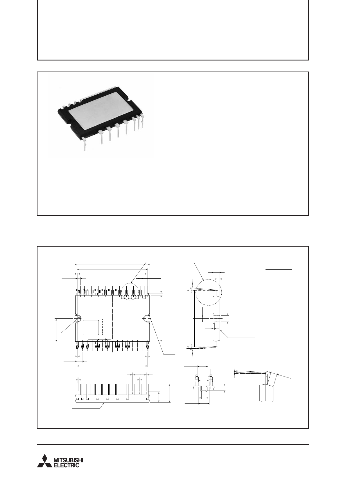
Fig. 1 PACKAGE OUTLINES (PS21965-4)
±0.5
38
20×1.778(=35.56)
0.28
±0.2
1.778
17 1
QR
2-R1.6
12
2.54
18
0.28
±0.2
0.5
HEAT SINK SIDE
Code
3 MIN
±0.3
35
Type name
Lot No.
14×2.54(=35.56)
A
16-0.5
(1)
±0.5
24
25
4-C1.2
8-0.6
0.50.5
0.5
±0.5
±0.5
9.5
5.5
B
3.5
±0.05
0.4
±0.5
14.4
(3.5)
±0.5
29.2
±0.5
14.4
0.4
2.5 MIN
(2.656)
(2.756)
DETAIL A DETAIL B
1.5
(3.3)
0.8
HEAT SINK SIDE
(0~5°)
(1.2)
(1.2)
Dimensions in mm
TERMINAL CODE
1. NC
2. V
UFB
3. V
VFB
4. V
WFB
5. U
P
6. V
P
7. W
P
8. V
P1
9. VNC *
10. U
N
11. V
N
12. W
N
13. V
N1
14. F
O
15. CIN
NC
*
16. V
17. NC
18. NC
19. NC
20. N
21. W
22. V
23. U
24. P
25. NC
1.5 MIN
*) Two VNC terminals (9 & 16 pin) are connected inside DIP-IPM, please connect either one to the 15V power supply GND outside and
leave another one open.
Aug. 2007
MITSUBISHI SEMICONDUCTOR <Dual-In-Line Package Intelligent Power Module>
PS21965-4/-4A/-4C/-4W
TRANSFER-MOLD TYPE
INSULATED TYPE
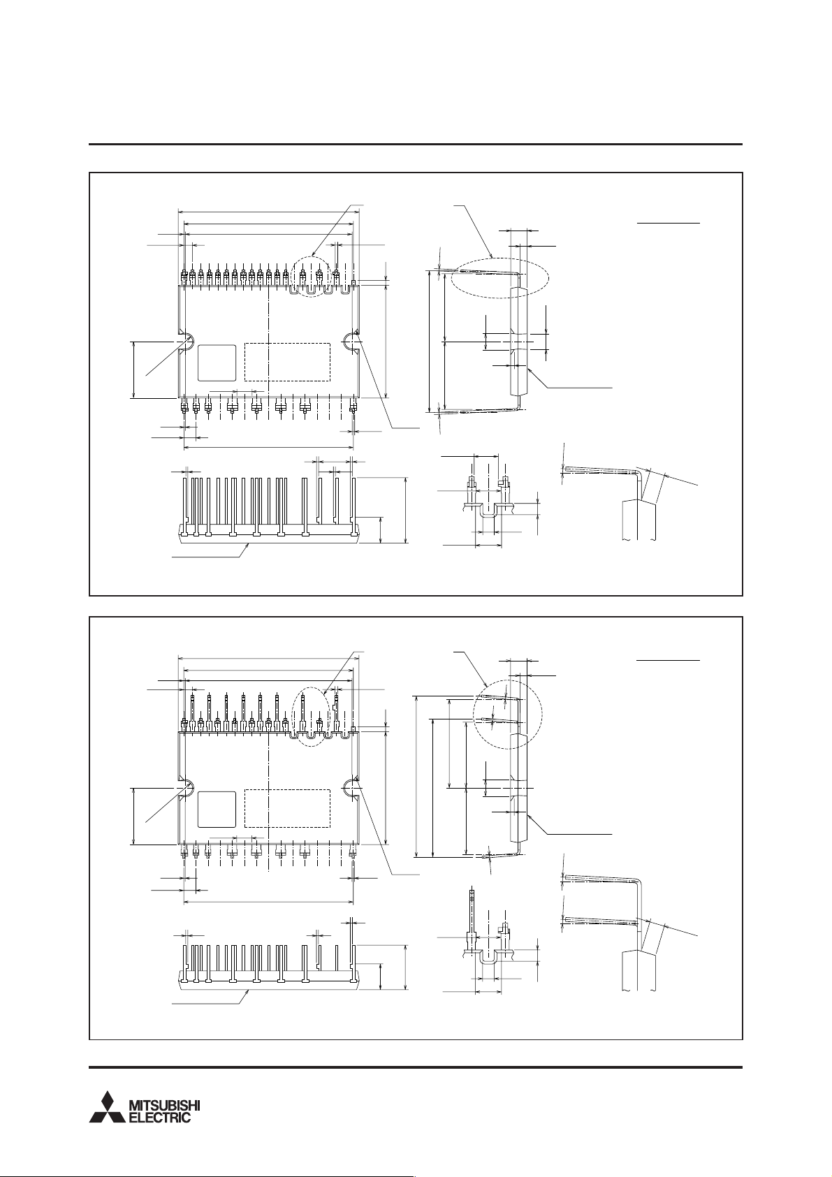
Fig. 2 LONG TERMINAL TYPE PACKAGE OUTLINES (PS21965-4A)
±0.5
38
20×1.778(=35.56)
1.778
0.28
±0.2
±0.3
35
A
16-0.5
B
3.5
±0.05
1.5
TERMINAL CODE
0.4
17 1
.6
1
-R
2
12
QR
Code
Type name
Lot No.
3 MIN
18
0.28
±0.2
2.54
14×2.54(=35.56)
0.5
0.5
(1)
±0.5
14.4
±0.5
±0.5
24
29.4
(3.5)
±0.5
0.8
14.4
25
4-C1.2
8-0.6
0.50.5
0.4
2.5 MIN
(3.3)
HEAT SINK SIDE
(0~5°)
(2.656)
±0.5
14
±0.5
5.5
(2.756)
HEAT SINK SIDE
NC terminals (9 & 16 pin) are connected inside DIP-IPM, please connect either one to the 15V power supply GND outside and
*) Two V
(1.2)
(1.2)
DETAIL A DETAIL B
leave another one open.
Dimensions in mm
1. NC
2. V
UFB
3. V
VFB
4. V
WFB
5. U
P
6. V
P
7. W
P
8. V
P1
9. VNC *
10. U
N
11. V
N
12. W
N
13. V
N1
14. F
O
15. CIN
16. V
NC
*
17. NC
18. NC
19. NC
20. N
21. W
22. V
23. U
24. P
25. NC
1.5 MIN
Fig. 3 ZIGZAG TERMINAL TYPE PACKAGE OUTLINES (PS21965-4C)
33.7
±0.5
29.2
±0.5
18.9
(2.656)
(2.756)
B
±0.5
14.4
±0.5
14.4
DETAIL A
±0.5
38
20×1.778(=35.56)
1.778
0.28
±0.2
±0.3
35
17 1
QR
2-R1.6
12
Code
Type name
Lot No.
3 MIN
18
0.28
±0.2
2.54
14×2.54(=35.56)
0.5
HEAT SINK SIDE
A
16-0.5
(1)
±0.5
±0.5
24
25
4-C1.2
8-0.6
0.5
0.5
±0.5
±0.5
9.5
5.5
(3.5)
3.5
±0.05
1.5
0.4
0.4
0.8
HEAT SINK SIDE
0.4
(0~5°)
(0~5°)
(1.2)
(1.2)
Dimensions in mm
TERMINAL CODE
1. NC
2. V
UFB
3. V
VFB
4. V
WFB
5. U
P
6. V
P
7. W
8. V
P1
9. VNC *
10. U
N
11. V
N
12. W
13. V
N1
14. F
O
15. CIN
16. V
NC
17. NC
18. NC
19. NC
20. N
21. W
22. V
23. U
24. P
25. NC
DETAIL B
P
N
*
1.5 MIN
*) Two VNC terminals (9 & 16 pin) are connected inside DIP-IPM, please connect either one to the 15V power supply GND outside and
leave another one open.
Aug. 2007
2
MITSUBISHI SEMICONDUCTOR <Dual-In-Line Package Intelligent Power Module>
PS21965-4/-4A/-4C/-4W
TRANSFER-MOLD TYPE
INSULATED TYPE
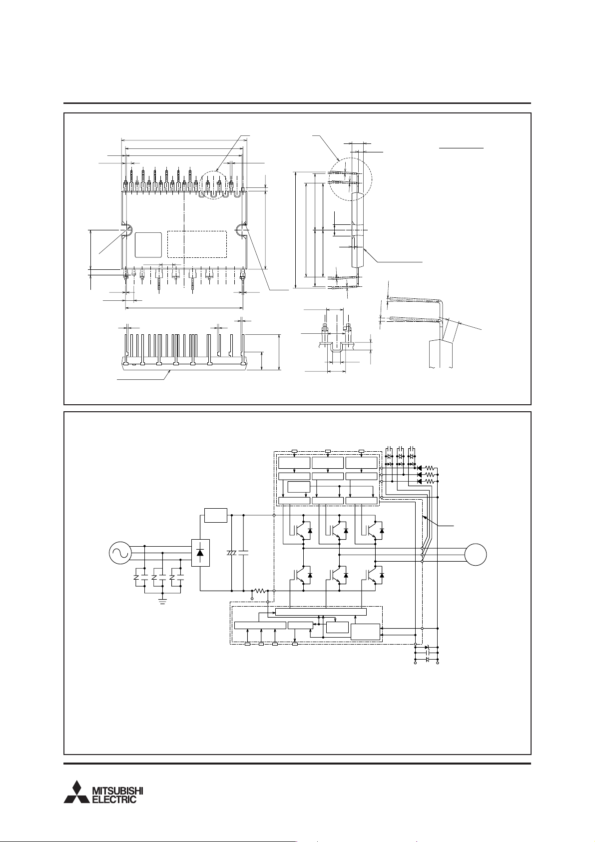
Fig. 4 BOTH SIDES ZIGZAG TERMINAL TYPE PACKAGE OUTLINES (PS21965-4W)
±0.6
35.2
B
3.5
±0.05
1.5
0.4
±0.5
14.4
±0.5
14.4
(3.5)
0.4
0.8
0.4
0.4
HEAT SINK SIDE
°)
(0~5
°)
(0~5
±0.5
17.4
±0.5
29.2
±0.5
17.4
2.5 MIN
(2.656)
(1.2)
(2.756)
(1.2)
DETAIL A DETAIL B
±0.5
38
20×1.778(=35.56)
1.778
0.28
±0.25
±0.3
35
17 1
QR
2-R1.6
12
Code
Type name
Lot No.
3 MIN
18
(1.8)
0.28
±0.25
2.54
14×2.54(=35.56)
0.5
HEAT SINK SIDE
A
16-0.5
(1)
±0.5
24
25
4-C1.2
7-0.6
0.5
0.5
±0.5
11
±0.5
5.5
TERMINAL CODE
1. NC
2. V
3. V
4. V
5. U
6. V
7. W
8. V
9. VNC *
10. U
11. V
12. W
13. V
14. F
15. CIN
16. V
17. NC
18. NC
19. NC
20. N
21. W
22. V
23. U
24. P
25. NC
Dimensions in mm
UFB
VFB
WFB
P
P
P
P1
N
N
N
N1
O
NC
*
1.5 MIN
*) Two VNC terminals (9 & 16 pin) are connected inside DIP-IPM, please connect either one to the 15V power supply GND outside and
leave another one open.
Fig. 5 INTERNAL FUNCTIONS BLOCK DIAGRAM (TYPICAL APPLICATION EXAMPLE)
CBU–
CBV–
CBW–
CBU+
CBV+
V
S
NC
CBW+
C2
C1
(Note 6)
S
U
V
W
(15V line)
(Note 7)
C1 : Electrolytic type with good temperature and frequency
characteristics
(Note : The capacitance value depends on the PWM control
scheme used in the applied system).
C2 : 0.22~2µF R-category ceramic capacitor for noise filtering.
Inrush current
limiter circuit
High-side input (PWM)
(3V, 5V line)(Note 1,
Input signal
conditioning
Level shifter
Protection
circuit (UV)
Drive circuit
P
2)
Input signal
conditioning
Level shifter
Drive circuit
Input signal
conditioning
Level shifter
Drive circuit
H-side IGBT
AC line input
(Note 4)
C
Z
Z : ZNR (Surge absorber)
C : AC filter (Ceramic capacitor 2.2~6.5nF)
(Note : Additionally, an appropriate line-to line
surge absorber circuit may become necessary
depending on the application environment).
Note1: Input logic is high-active. There is a 3.3kΩ (min) pull-down resistor built-in each input circuit. When using an external CR filter, please make it satisfy the
input threshold voltage.
2: By virtue of integrating an application specific type HVIC inside the module, direct coupling to MCU terminals without any opto-coupler or transformer
isolation is possible. (see also Fig. 11)
3: This output is open drain type. The signal line should be pulled up to the positive side of the 5V power supply with approximately 10kΩ resistor.
(see also Fig. 11)
4: The wiring between the power DC link capacitor and the P, N1 terminals should be as short as possible to protect the DIP-IPM against catastrophic high
surge voltages. For extra precaution, a small film type snubber capacitor (0.1~0.22µF, high voltage type) is recommended to be mounted close to
these P & N1 DC power input pins.
5: High voltage (600V or more) and fast recovery type (less than 100ns) diodes should be used in the bootstrap circuit.
6: It is recommended to insert a Zener diode (24V/1W) between each pair of control supply terminals to prevent surge destruction.
7: Bootstrap negative electrodes should be connected to U, V, W terminals directly and separated from the main output wires.
N1
N
V
NC
CIN
Input signal conditioning
Low-side input (PWM)
(3V, 5V line)(Note 1, 2)
Drive circuit
Fo logic
F
O
Fault output (5V line)
(Note 3)
Protection
circuit
Control supply
Under-Voltage
protection
L-side IGBT
(Note 5)
DIP-IPM
AC line output
(Note 6)
V
D
M
Aug. 2007
3

MITSUBISHI SEMICONDUCTOR <Dual-In-Line Package Intelligent Power Module>
Fig. 6 EXTERNAL PART OF THE DIP-IPM PROTECTION CIRCUIT
PS21965-4/-4A/-4C/-4W
TRANSFER-MOLD TYPE
INSULATED TYPE
DIP-IPM
P
H-side IGBT
External protection circuit
Shunt Resistor
N1
(Note 1)
R
C
C
Note1: In the recommended external protection circuit, please select the RC time constant in the range 1.5~2.0µs.
2: To prevent erroneous protection operation, the wiring of A, B, C should be as short as possible.
L-side IGBT
A
N
NC
V
CIN
B
(Note 2)
Drive circuit
S
S
Drive circuit
Protection circuit
Short Circuit Protective Function (SC) :
SC protection is achieved by sensing the L-side DC-Bus current (through the external
shunt resistor) after allowing a suitable filtering time (defined by the RC circuit).
When the sensed shunt voltage exceeds the SC trip-level, all the L-side IGBTs are turned
OFF and a fault signal (Fo) is output. Since the SC fault may be repetitive, it is
recommended to stop the system when the Fo signal is received and check the fault.
IC (A)
U
V
W
0
Collector current
waveform
2
SC Protection
Trip Level
w
(µs)
t
MAXIMUM RATINGS (Tj = 25°C, unless otherwise noted)
INVERTER PART
ConditionSymbol
(Note 1)
V
CC
VCC(surge)
VCES
±IC
±ICP
PC
Tj
Parameter
Supply voltage
Supply voltage (surge)
Collector-emitter voltage
Each IGBT collector current
Each IGBT collector current (peak)
Collector dissipation
Junction temperature
Applied between P-N
Applied between P-N
T
C = 25°C
C = 25°C, less than 1ms
T
C = 25°C, per 1 chip
T
Note 1 : The maximum junction temperature rating of the power chips integrated within the DIP-IPM is 150°C (@ TC ≤ 100°C). However, to
ensure safe operation of the DIP-IPM, the average junction temperature should be limited to Tj(ave) ≤ 125°C (@ TC ≤ 100°C).
Ratings Unit
450
500
600
20
40
35.7
–20~+125
V
V
V
A
A
W
°C
CONTROL (PROTECTION) PART
Parameter
V
D
VDB
VIN
VFO
IFO
VSC
Control supply voltage
Control supply voltage
Input voltage
Fault output supply voltage
Fault output current
Current sensing input voltage
ConditionSymbol
Applied between V
P1-VNC, VN1-VNC
Applied between VUFB-U, VVFB-V, VWFB-W
Applied between U
P, VP, WP, UN, VN,
WN-VNC
Applied between FO-VNC
Sink current at FO terminal
Applied between CIN-V
NC
4
Ratings Unit
20
20
D+0.5
–0.5~V
D+0.5
–0.5~V
1
–0.5~V
D+0.5
Aug. 2007
V
V
V
V
mA
V

MITSUBISHI SEMICONDUCTOR <Dual-In-Line Package Intelligent Power Module>
PS21965-4/-4A/-4C/-4W
TRANSFER-MOLD TYPE
INSULATED TYPE
TOTAL SYSTEM
Symbol Ratings Unit
V
CC(PROT)
TC
Tstg
Viso
Self protection supply voltage limit
(short circuit protection capability)
Module case operation temperature
Storage temperature
Isolation voltage
Parameter
D = 13.5~16.5V, Inverter part
V
Tj = 125°C, non-repetitive, less than 2µs
60Hz, Sinusoidal, 1 minute,
Between pins and heat-sink plate
Condition
(Note 2)
400
–20~+100
–40~+125
1500
V
°C
°C
rms
V
Note 2: T
C measurement point
IGBT chip position
FWD chip position
Control terminals
11.6mm
Power terminals
3mm
C
point
T
Heat sink side
DIP-IPM
THERMAL RESISTANCE
Parameter
Rth(j-c)Q
Rth(j-c)F
Note 3 : Grease with good thermal conductivity should be applied evenly with about +100µm~+200µm on the contacting surface of DIP-IPM
Junction to case thermal
resistance (Note 3)
and heat-sink.
The contacting thermal resistance between DIP-IPM case and heat sink (R
conductivity of the applied grease. For reference, R
the thermal conductivity is 1.0W/m·k.
Inverter IGBT part (per 1/6 module)
Inverter FWD part (per 1/6 module)
ConditionSymbol
th(c-f) (per 1/6 module) is about 0.3°C/W when the grease thickness is 20µm and
th(c-f)) is determined by the thickness and the thermal
Min.
Limits
Typ. Max.
—
—
—
—
2.8
3.9
Unit
°C/W
°C/W
ELECTRICAL CHARACTERISTICS (Tj = 25°C, unless otherwise noted)
INVERTER PART
Symbol
CE(sat)
V
VEC
ton
trr
tc(on)
toff
tc(off)
ICES
Parameter
Collector-emitter saturation
voltage
FWD forward voltage
Switching times
Collector-emitter cut-off
current
Condition
I
VD = VDB = 15V
VIN = 5V
C = 20A, Tj = 25°C
IC = 20A, Tj = 125°C
Tj = 25°C, –IC = 20A, VIN = 0V
CC = 300V, VD = VDB = 15V
V
IC = 20A, Tj = 125°C, VIN = 0 ↔ 5V
Inductive load (upper-lower arm)
T
CE = VCES
V
j = 25°C
Tj = 125°C
Limits
Min. Typ. Max.
—
—
—
0.70
—
—
—
—
—
—
1.70
1.80
1.90
1.30
0.30
0.50
1.60
0.40
—
—
2.20
2.30
2.40
1.90
0.75
2.20
0.75
—
10
Unit
V
V
µs
µs
µs
µs
µs
1
mA
Aug. 2007
5

MITSUBISHI SEMICONDUCTOR <Dual-In-Line Package Intelligent Power Module>
PS21965-4/-4A/-4C/-4W
TRANSFER-MOLD TYPE
INSULATED TYPE
CONTROL (PROTECTION) PART
—
—
—
—
4.9
—
20
—
0.8
Limits
—
—
—
—
—
—
0.48
1.00
—
—
—
—
—
2.1
1.3
0.65
2.80
0.55
2.80
0.55
0.95
0.53
1.50
12.0
12.5
12.5
13.0
Symbol
I
D
VFOH
VFOL
VSC(ref)
IIN
UVDBt
UVDBr
UVDt
UVDr
tFO
Vth(on)
Vth(off)
Vth(hys)
Parameter Condition
Circuit current
Fault output voltage
Short circuit trip level
Input current
Control supply under-voltage
protection
Fault output pulse width
ON threshold voltage
OFF threshold voltage
ON/OFF threshold hysteresis
voltage
D = VDB = 15V
V
V
IN = 5V
V
D = VDB = 15V
V
IN = 0V
V
SC = 0V, FO terminal pull-up to 5V by 10kΩ
V
SC = 1V, IFO = 1mA
T
j = 25°C, VD = 15V (Note 4)
V
IN = 5V
Total of V
VUFB-U, VVFB-V, VWFB-W
Total of V
VUFB-U, VVFB-V, VWFB-W
P1-VNC, VN1-VNC
P1-VNC, VN1-VNC
Trip level
T
j ≤ 125°C
Reset level
Trip level
Reset level
(Note 5)
Applied between U
P, VP, WP, UN, VN, WN-VNC
Min. Typ. Max.
0.43
0.70
10.0
10.5
10.3
10.8
0.35
Note 4 : Short circuit protection is functioning only for the lower-arms. Please select the external shunt resistance such that the SC trip-level is
less than 1.7 times of the current rating.
5:Fault signal is asserted corresponding to a short circuit or lower side control supply under-voltage failure.
—
—
2.6
—
—
Unit
mA
mA
mA
mA
V
V
V
mA
V
V
V
V
µs
V
V
V
MECHANICAL CHARACTERISTICS AND RATINGS
Parameter
Mounting torque
Weight
Heat-sink flatness
Note 6 : Plain washers (ISO 7089~7094) are recommended.
Note 7: Flatness measurement position
+–
Heat sink side
Mounting screw : M3
Measurement position
–
+
Condition
(
)
Note 6
4.6mm
DIP-IPM
Heat sink side
Recommended : 0.69 N·m
(
Note 7
Limits
Min.
0.59
—
)
–50
Typ. Max.
—
0.78
10
—
100
Unit
N·m
—
g
µm
Aug. 2007
6

MITSUBISHI SEMICONDUCTOR <Dual-In-Line Package Intelligent Power Module>
PS21965-4/-4A/-4C/-4W
RECOMMENDED OPERATION CONDITIONS
Parameter
CC
V
VD
VDB
∆VD, ∆VDB
tdead
fPWM
I
O
PWIN(on)
PWIN(off)
NC
V
Supply voltage
Control supply voltage
Control supply voltage
Control supply variation
Arm shoot-through blocking time
PWM input frequency
Allowable r.m.s. current
Allowable minimum input
pulse width
NC variation
V
Applied between P-N
Applied between V
Applied between VUFB-U, VVFB-V, VWFB-W
For each input signal, T
T
C ≤ 100°C, Tj ≤ 125°C
V
CC = 300V, VD = VDB = 15V,
P.F = 0.8, sinusoidal PWM,
j ≤ 125°C, TC ≤ 100°C (Note 8)
T
Between V
NC-N (including surge)
Note 8 : The allowable r.m.s. current value depends on the actual application conditions.
9:IPM might not make response if the input signal pulse width is less than the recommended minimum value.
Fig. 7 THE DIP-IPM INTERNAL CIRCUIT
ConditionSymbol
P1-VNC, VN1-VNC
C ≤ 100°C
PWM = 5kHz
f
fPWM = 15kHz——
(Note 9)
TRANSFER-MOLD TYPE
INSULATED TYPE
Limits
Min. Typ. Max.
0
13.5
13.0
–1
1.5
—
0.5
0.5
–5.0
300
15.0
15.0
—
—
—
—
—
—
—
—
400
16.5
18.5
1
—
20
10.0
6.0
—
—
5.0
Unit
V
V
V
V/µs
µs
kHz
Arms
µs
V
V
UFB
HVIC
V
LVIC
UB
U
OUT
V
US
V
OUT
V
VS
W
OUT
V
WS
U
OUT
V
OUT
W
OUT
CIN
V
NO
V
V
P1
U
P
V
NC
V
VFB
V
P
V
WFB
W
P
V
N1
U
N
V
N
W
N
Fo
V
NC
CC
U
P
COM
V
VB
V
P
V
WB
W
P
V
CC
U
N
V
N
N
W
Fo
GND
IGBT1
IGBT2
IGBT3
IGBT4
IGBT5
IGBT6
Di1
Di2
Di3
Di4
Di5
Di6
DIP-IPM
P
U
V
W
N
CIN
Aug. 2007
7

MITSUBISHI SEMICONDUCTOR <Dual-In-Line Package Intelligent Power Module>
PS21965-4/-4A/-4C/-4W
TRANSFER-MOLD TYPE
Fig. 8 TIMING CHART OF THE DIP-IPM PROTECTIVE FUNCTIONS
[A] Short-Circuit Protection (Lower-side only with the external shunt resistor and CR filter)
a1. Normal operation : IGBT ON and carrying current.
a2. Short circuit detection (SC trigger).
a3. IGBT gate hard interruption.
a4. IGBT turns OFF.
O outputs (tFO(min) = 20µs).
a5. F
a6. Input “L” : IGBT OFF.
a7. Input “H” : IGBT ON.
a8. IGBT OFF in spite of input “H”.
INSULATED TYPE
Lower-side control
input
Protection circuit state
Internal IGBT gate
SET
a3
a7a6
RESET
a2
Output current Ic
Sense voltage of the
shunt resistor
a1
SC
a4
a8
SC reference voltage
CR circuit time
Error output Fo
a5
constant DELAY
[B] Under-Voltage Protection (Lower-side, UVD)
b1. Control supply voltage rising : After the voltage level reaches UVDr, the circuits start to operate when next input is applied.
b2. Normal operation : IGBT ON and carrying current.
b3. Under voltage trip (UVDt).
b4. IGBT OFF in spite of control input condition.
b5. FO outputs (tFO ≥ 20µs and FO outputs continuously during UV period).
b6. Under voltage reset (UVDr).
b7. Normal operation : IGBT ON and carrying current.
Control input
Protection circuit state
Control supply voltage V
Output current Ic
Error output Fo
RESET
UV
Dr
D
b1
UV
Dt
b2
SET
b3
b4
RESET
b6
b7
b5
Aug. 2007
8

MITSUBISHI SEMICONDUCTOR <Dual-In-Line Package Intelligent Power Module>
PS21965-4/-4A/-4C/-4W
TRANSFER-MOLD TYPE
INSULATED TYPE
[C] Under-Voltage Protection (Upper-side, UVDB)
c1. Control supply voltage rising : After the voltage level reaches UVDBr, the circuits start to operate when next input is applied.
c2. Normal operation : IGBT ON and carrying current.
c3. Under voltage trip (UVDBt).
c4. IGBT OFF in spite of control input signal level, but there is no FO signal outputs.
c5. Under voltage reset (UVDBr).
c6. Normal operation : IGBT ON and carrying current.
Control input
Protection circuit state
UVDBr
Control supply voltage V
DB
c1
Output current Ic
High-level (no fault output)
Error output Fo
Fig. 9 RECOMMENDED MCU I/O INTERFACE CIRCUIT
5V line
MCU
UV
DBt
c2 c4
10kΩ
SETRESET
RESET
c5
c3
c6
DIP-IPM
P,VP,WP,UN,VN,WN
U
Fo
VNC(Logic)
3.3kΩ (min)
Note : The setting of RC coupling at each input (parts shown dotted) depends on the PWM control scheme and the
wiring impedance of the printed circuit board.
The DIP-IPM input section integrates a 3.3kΩ (min) pull-down resistor. Therefore, when using an external
filtering resistor, pay attention to the turn-on threshold voltage.
Fig. 10 WIRING CONNECTION OF SHUNT RESISTOR
DIP-IPM
V
NC
N
Wiring inductance should be less than 10nH.
Equivalent to the inductance of a copper
pattern in dimension of width=3mm,
thickness=100µm, length=17mm
Shunt resistor
Please make the GND wiring connection
of shunt resistor to the V
as close as possible.
9
NC
terminal
Aug. 2007

MITSUBISHI SEMICONDUCTOR <Dual-In-Line Package Intelligent Power Module>
Fig. 11 AN EXAMPLE OF TYPICAL DIP-IPM APPLICATION CIRCUIT
C1: Electrolytic capacitor with good temperature characteristics
0.22~2µF R-category ceramic capacitor for noise filteringC2,C3:
C2C2C2C1
V
UFBVVFBVWFB
V
C3
P1
U
P
V
P
HVIC
V
CC
V
UB
P
U
OUT
U
V
US
V
VB
V
OUT
V
P
V
VS
C1
C1
DIP-IPM
PS21965-4/-4A/-4C/-4W
TRANSFER-MOLD TYPE
INSULATED TYPE
Bootstrap negative
electrodes should be
connected to U, V, W
terminals directly and
separated from the
P
U
V
main output wires.
MM
V
MCU
W
P
V
NC
W
COM
WB
W
OUT
P
V
WS
W
LVIC
OUT
5V line
V
N1
C3
U
N
V
N
N
W
Fo
V
NC
V
CC
U
N
V
N
W
F
o
GND
U
V
OUT
Long wiring here might
N
W
OUT
Long wiring here might
cause short-circuit.
cause short-circuit.
N
C
CIN
15V line
Long GND wiring here might
generate noise to input and
cause IGBT malfunction.
A
C4
B
R1
Shunt
resistor
N1
Long wiring here might cause SC
level fluctuation and malfunction.
Note 1 : Input drive is High-Active type. There is a 3.3kΩ(min.) pull-down resistor integrated in the IC input circuit. To prevent malfunction, the
wiring of each input should be as short as possible. When using RC coupling circuit, make sure the input signal level meet the turn-on
and turn-off threshold voltage.
2:Thanks to HVIC inside the module, direct coupling to MCU without any opto-coupler or transformer isolation is possible.
3:FO output is open drain type. It should be pulled up to the positive side of a 5V power supply by a resistor of about 10kΩ.
4:To prevent erroneous protection, the wiring of A, B, C should be as short as possible.
5:The time constant R1C4 of the protection circuit should be selected in the range of 1.5-2µs. SC interrupting time might vary with the
wiring pattern. Tight tolerance, temp-compensated type is recommended for R1, C4.
6:All capacitors should be mounted as close to the terminals of the DIP-IPM as possible. (C1: good temperature, frequency character-
istic electrolytic type, and C2, C3: good temperature, frequency and DC bias characteristic ceramic type are recommended.)
7:To prevent surge destruction, the wiring between the smoothing capacitor and the P, N1 terminals should be as short as possible.
Generally a 0.1-0.22µF snubber between the P-N1 terminals is recommended.
8:Two VNC terminals (9 & 16 pin) are connected inside DIP-IPM, please connect either one to the 15V power supply GND outside and
leave another one open.
9:It is recommended to insert a Zener diode (24V/1W) between each pair of control supply terminals to prevent surge destruction.
10 : If control GND is connected to power GND by broad pattern, it may cause malfunction by power GND fluctuation. It is recommended
to connect control GND and power GND at only a point.
10
Aug. 2007
 Loading...