

MITSUBISHI PS21963-ST Technical data
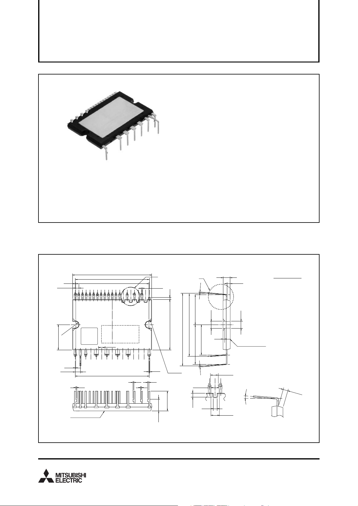
MITSUBISHI SEMICONDUCTOR <Dual-In-Line Package Intelligent Power Module>
PS21963-ST
TRANSFER-MOLD TYPE
INSULATED TYPE
PS21963-ST
INTEGRATED POWER FUNCTIONS
600V/10A low-loss 5th generation IGBT inverter bridge for
three phase DC-to-AC power conversion.
Open emitter type.
INTEGRATED DRIVE, PROTECTION AND SYSTEM CONTROL FUNCTIONS
• For upper-leg IGBTS : Drive circuit, High voltage high-speed level shifting, Control supply under-voltage (UV) protection.
• For lower-leg IGBTS :
Drive circuit, Control supply under-voltage protection (UV), Short circuit protection (SC), Over temperature protection (OT).
• Fault signaling : Corresponding to an SC fault (Lower-leg IGBT), a UV fault (Lower-side supply) or an OT fault (LVIC temperature).
• Input interface : 3V, 5V line (High Active).
•UL Approved : Yellow Card No. E80276
APPLICATION
AC100V~200V inverter drive for small power motor control.
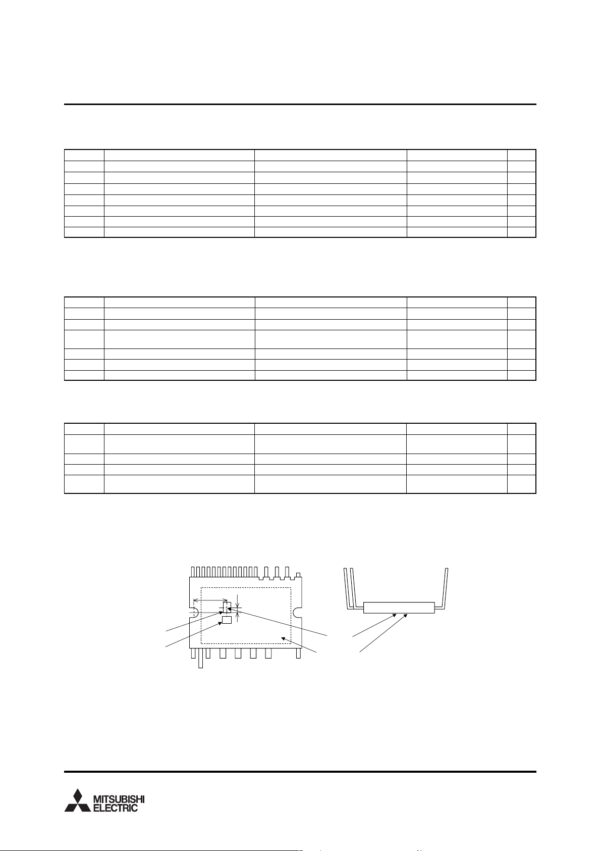
Fig. 1 PACKAGE OUTLINES
QR
Code
20×1.778(=35.56 )
Type name
Lot No.
14×2.54(=35.56)
0.28
±0.2
1.778
17 1
2-R1.6
12
18
0.28
±0.2
2.54
0.5
HEAT SINK SIDE
38
35
3 MIN
±0.5
±0.3
0.5 0.5
A
16-0.5
(1)
±0.5
±0.5
24
33.7
25
8-0.6
0.5
4-C1.2
±0.5
9.5
±0.5
5.5
±0.5
29.2
±0.5
14.4
±0.5
18.9
(2.656)
(1.2)
B
0.4
±0.5
14.4
0.4
(1.2)
3.5
±0.05
1.5
(3.5)
0.8
2.5 MIN
DETAIL A DETAIL B
(3.3)
HEAT SINK SIDE
(0°~5°)
(2.756)
Dimensions in mm
TERMINAL CODE
1. (VNC)
2. VUFB
3. VVFB
4. VWFB
5. UP
6. VP
7. WP
8. VP1
9. VNC *
10. UN
11. VN
12. WN
13. VN1
14. FO
15. CIN
16. VNC *
17. NC
18. NW
19. NV
20. NU
21. W
22. V
23. U
24. P
25. NC
1.5min
*) Two VNC terminals (9 & 16 pin) are connected inside DIPIPM, please connect either one to the 15V power supply GND outside and
leave another one open.
QR Code is registered trademark of DENSO WAVE INCORPORATED in Japan and other countries.
Mar. 2009
MITSUBISHI SEMICONDUCTOR <Dual-In-Line Package Intelligent Power Module>
PS21963-ST
TRANSFER-MOLD TYPE
INSULATED TYPE
MAXIMUM RATINGS (Tj = 25°C, unless otherwise noted)
INVERTER PART
ConditionSymbol Parameter Ratings Unit
CC
V
VCC(surge)
VCES
±IC
±ICP
PC
Tj
Supply voltage
Supply voltage (surge)
Collector-emitter voltage
Each IGBT collector current
Each IGBT collector current (peak)
Collector dissipation
Junction temperature
Applied between P-NU, NV, NW
Applied between P-NU, NV, NW
C = 25°C
T
T
C = 25°C, less than 1ms
C = 25°C, per 1 chip
T
(Note 1)
450
500
600
10
20
27.0
–20~+125
Note 1 : The maximum junction temperature rating of the power chips integrated within the DIPIPM is 150°C (@ TC ≤ 100°C). However, to en-
sure safe operation of the DIPIPM, the average junction temperature should be limited to T
j(ave) ≤ 125°C (@ TC ≤ 100°C).
CONTROL (PROTECTION) PART
V
D
VDB
VIN
VFO
IFO
VSC
Parameter
Control supply voltage
Control supply voltage
Input voltage
Fault output supply voltage
Fault output current
Current sensing input voltage
ConditionSymbol
Applied between V
P1-VNC, VN1-VNC
Applied between VUFB-U, VVFB-V, VWFB-W
Applied between U
P, VP, WP, UN, VN,
W
N-VNC
Applied between FO-VNC
Sink current at FO terminal
Applied between CIN-V
NC
Ratings Unit
20
20
D+0.5
–0.5~V
–0.5~V
D+0.5
1
D+0.5
–0.5~V
V
V
V
A
A
W
°C
V
V
V
V
mA
V
TOTAL SYSTEM
Symbol Ratings Unit
CC(PROT)
V
TC
Tstg
Viso
Note 2: T
Self protection supply voltage limit
(short circuit protection capability)
Module case operation temperature
Storage temperature
Isolation voltage
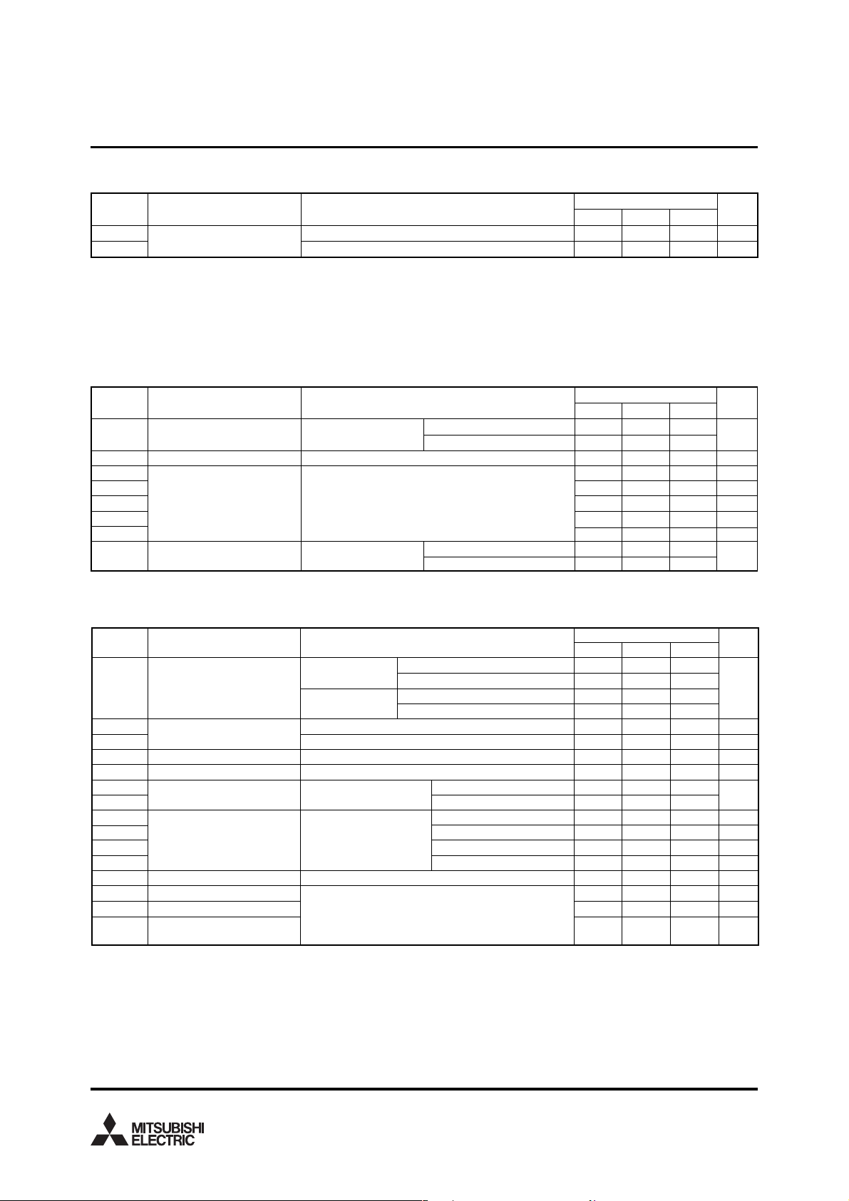
C measurement point
IGBT chip position
FWD chip position
Parameter
Control terminals
11.6mm
Power terminals
D = 13.5~16.5V, Inverter part
V
j = 125°C, non-repetitive, less than 2µs
T
60Hz, Sinusoidal, 1 minute,
Between pins and heat-sink plate
3mm
Condition
C
point
T
Heat sink side
(Note 2)
400
–20~+100
–40~+125
1500
V
°C
°C
rms
V
Mar. 2009
2
MITSUBISHI SEMICONDUCTOR <Dual-In-Line Package Intelligent Power Module>
PS21963-ST
TRANSFER-MOLD TYPE
INSULATED TYPE
THERMAL RESISTANCE
ConditionSymbol Parameter
Rth(j-c)Q
Rth(j-c)F
Note 3 : Grease with good thermal conductivity should be applied evenly with about +100µm~+200µm on the contacting surface of DIPIPM and
Junction to case thermal
resistance (Note 3)
heat-sink.
The contacting thermal resistance between DIPIPM case and heat sink (R
ductivity of the applied grease. For reference, R
the thermal conductivity is 1.0W/m·k.
Inverter IGBT part (per 1/6 module)
Inverter FWD part (per 1/6 module)
th(c-f) (per 1/6 module) is about 0.3°C/W when the grease thickness is 20µm and
th(c-f)) is determined by the thickness and the thermal con-
Min.
Limits
Typ. Max.
—
—
—
—
ELECTRICAL CHARACTERISTICS (Tj = 25°C, unless otherwise noted)
INVERTER PART
Symbol Parameter
V
CE(sat)
VEC
Collector-emitter saturation
voltage
FWD forward voltage
ton
trr
tc(on)
Switching times
toff
tc(off)
ICES
Collector-emitter cut-off
current
Condition
VD = VDB = 15V
VIN = 5V
C = 10A, Tj = 25°C
I
IC = 10A, Tj = 125°C
Tj = 25°C, –IC = 10A, VIN = 0V
CC = 300V, VD = VDB = 15V
V
IC = 10A, Tj = 125°C, VIN = 0 ↔ 5V
Inductive load (upper-lower arm)
T
CE = VCES
V
j = 25°C
Tj = 125°C
Min. Typ. Max.
0.60
Limits
—
1.70
—
1.80
—
1.70
1.10
—
0.30
—
0.40
—
1.50
—
0.50
—
—
2.20
2.30
2.20
1.70
0.60
2.10
0.80
—
—
3.7
4.5
—
10
Unit
°C/W
°C/W
Unit
V
V
µs
µs
µs
µs
µs
1
mA
CONTROL (PROTECTION) PART
—
—
—
—
4.9
—
—
20
—
0.8
Limits
—
—
—
—
—
—
0.48
1.00
120
10
—
—
—
—
—
2.1
1.3
0.65
2.80
0.55
2.80
0.55
0.95
0.53
1.50
12.0
12.5
12.5
13.0
Symbol
I
D
VFOH
VFOL
VSC(ref)
IIN
OTt
OTrh
UVDBt
UVDBr
UVDt
UVDr
tFO
Vth(on)
Vth(off)
Vth(hys)
Parameter Condition
Circuit current
Fault output voltage
Short circuit trip level
Input current
Over temperature protection
(Note 5)
Control supply under-voltage
protection
Fault output pulse width
ON threshold voltage
OFF threshold voltage
ON/OFF threshold hysteresis
voltage
V
D = VDB = 15V
IN = 5V
V
V
D = VDB = 15V
V
IN = 0V
SC = 0V, FO terminal pull-up to 5V by 10kΩ
V
SC = 1V, IFO = 1mA
V
T
j = 25°C, VD = 15V (Note 4)
IN = 5V
V
VD = 15V,
At temperature of LVIC
Total of V
P1-VNC, VN1-VNC
VUFB-U, VVFB-V, VWFB-W
Total of V
P1-VNC, VN1-VNC
VUFB-U, VVFB-V, VWFB-W
Trip level
Trip/reset hysteresis
Trip level
T
j ≤ 125°C
Reset level
Trip level
Reset level
(Note 6)
Applied between U
P, VP, WP, UN, VN, WN-VNC
Min. Typ. Max.
0.43
0.70
100
10.0
10.5
10.3
10.8
0.35
Note 4 : Short circuit protection is functioning only for the lower-arms. Please select the external shunt resistance such that the SC trip-level is
less than 1.7 times of the current rating.
5:Over temperature protection (OT) outputs fault signal, when the LVIC temperature exceeds OT trip temperature level (OTt). In that case
if the heat sink comes off DIPIPM or fixed loosely, don’t reuse that DIPIPM. (There is a possibility that junction temperature of power chips
exceeded maximum Tj (150°C)).
6:Fault signal is asserted only corresponding to a SC, a UV or an OT failure at lower side, and the F
ure modes. For SC failure, F
whole UV or OT period, however, the minimum F
O output is with a fixed width of 20µsec(min), but for UV or OT failure, FO output continuously during the
O pulse width is 20µsec(min) for very short UV or OT period less than 20µsec.
O pulse width is different for each fail-
—
140
—
—
2.6
—
—
Unit
mA
V
V
V
mA
°C
V
V
V
V
µs
V
V
V
Mar. 2009
3
 Loading...