


Mitsubishi MA1046-1 Datasheet
MA1046-1
No. Items
Frequency
1
2
8
11
Power Gain
Occupied Band Width
Stability against
load variation
Symbol
f
G
3
Temperature
Characteristics (Power Gain)
– – –
Unit
MHz
dB
mA
mA
Standard
Condition
4
Gain Variation
∆ G
mA5 Drain Current ID 12
ID 3
6 Gate Current IG 12
IG 3
– – –
ACP1
ACP2
mA
1918
– – –
2
5
400
1400
– – –
– – –
– – –
– – –
– – –
– – –
1895
MaxTypeMin
33
dB±2– – –– – –
dB±0.5– – –– – –
– – –
– – –
dBc–65– – –– – –
– – –
– – –
f
<
=
6 GHz
9 Input VSWR
ρ in
dBc–70– – –– – –
KHz288– – –– – –
– – –2.0– – –– – –
dBc–70– – –– – –
dBc–60– – –– – –
dBc–30– – –– – –
dBc–45– – –– – –
Po = +35 dBm
Non-modulation
Po = +35 dBm
π / 4 Shift QPSK Modulation –PN9
Po = +35 dBm Load VSWR = 1:3
All Phase
Po = +35 dBm Zl = OPEN, SHORT
10 seconds each
7 ∆ 600 kHzACP
∆ 900 kHz
– – –
– – –
10 In BandSpurious
Out Band
2 SP
3 SP
2 nd
3 rd
12 Intensity against
load variation
– – –
There is no abnormal oscillating
signal more than –60 dBc
There is no damage
MA1046-1
adefgh
i
bc
58
0.5
55510
50 Max.
5810
1.8
57
62 Max.
3.6
10
19.5
RF IN
GND
V
G12
VD12
GND
V
G3
VD3
RF OUT
GND (base)
8 Max.
2.5
2
4
25 Max.
21 Max.
1.2
Unit : mm
1
2
3
4
5
6
7
8
9
No. Condition
Case temperature
1
2
3
4
5
Storage temperature
Voltage
Gate Voltage
Input Power
SymbolItems
Tc
Tstg
VD12, VD 3
VG 12, VG 3
Pin
Unit
°C
°C
V
V
dBm
VG 12 = –5.0 V, VG 3 = –3.0 V
VD 12 = 6.0 V, VD 3 = 10.0 V
Standard
–20 ~ +70
–40 ~ +95
V
D 12 = 7.0 V, VD 3 = 11.0 V
V
G 12 = –8.0 V, VG = –8.0 V
+10 dBm
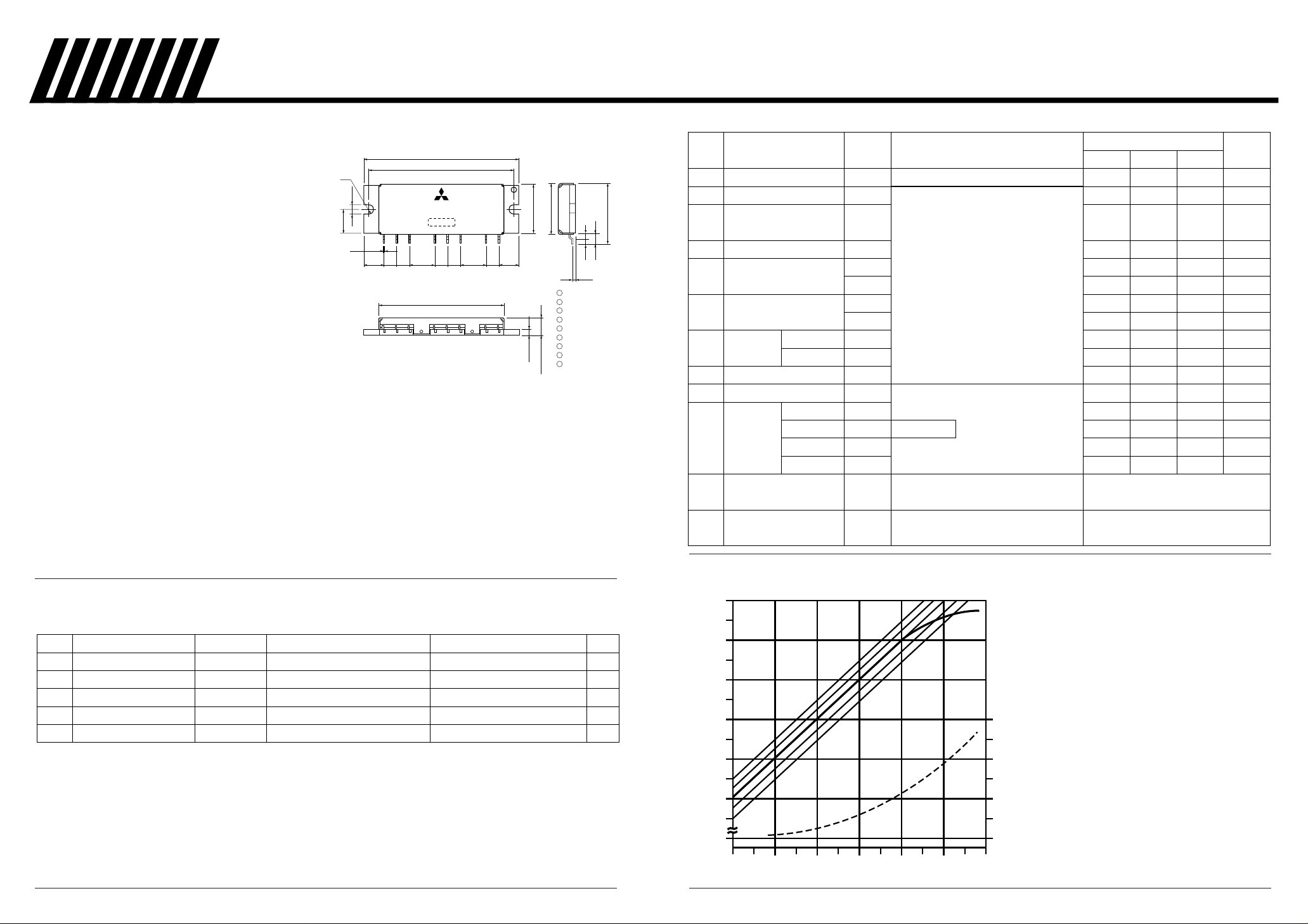
–11
19
23
27
31
35
39
20
0
40
60
–7 –3
Input Power [dBm]
159
Additional Effciency [%]
Output Power [dBm]
PO
Typical Characteristics
VD12 = 6 V, VD3 = 10 V
VG12 = –5 V, VG3 = –3 V
η
For 1.9 GHz - Power Amplifier
MA1046-1
DESCRIPTION
The MA1046-1 is a 1.9 GHz band power
amplifier (Po = +3.1W), constructed by 3 stages
of GaAs MESFET, RF matching circuit, and DC
bias circuit. The shield cap is made of metal.
Input and Output impedances are designed to
50Ω.
FEATURES
Po = +35.0 dBm, Gain = +32 dB (min.) @1.9 GHz
Vd1, 2 = +6.0V, Vd3 = +10.0V
Vg1, 2 = –5.0V, Vg3 = 3.0V
APPLICATION
Power amplifier for PHS base station/Japan.
OUTLINE DRAWING
Note: 1. Dimension of leads: 0.25 × 0.5
2. Tolerance of dimension of leads interval: ±0.3
3. Tolerance of dimension except indications: ±0.3
4. Surface Leads: Tin Plating (Iron)
(Material)
2. Electrical Performances
(Tc = +25°C, VD 1, 2 = 6V, VD3 = 10V, VG 1, 2 = –5V, VG 3 = –3V, Zg = Zl = 50Ω)
Amplifier Specifications (MA1046-1)
1. Maximum Ratings (Ta=25°C)
MA1046-1 Pin – Pout. ACP.
– 89 –– 88 –