

PRELIMINARY
Notice: This is not a final specification.
Some parametric limits are subject to change.
MITSUBISHI SEMICONDUCTORS <HVIC>
M81719FP
HIGH VOLTAGE HALF BRIDGE DRIVER
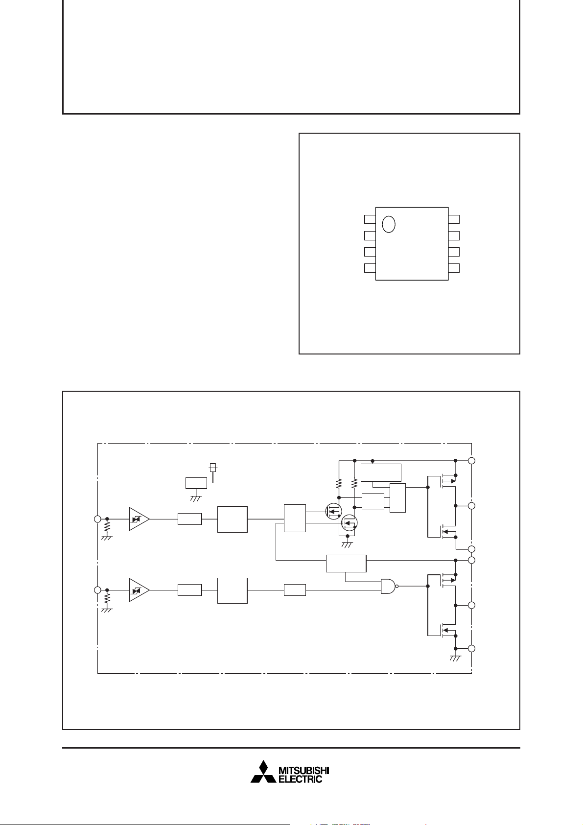
DESCRIPTION
M81719FP is high voltage Power MOSFET and IGBT module driver for half bridge applications.
FEATURES
¡FLOATING SUPPLY VOLTAGE ................................. 600V
¡OUTPUT CURRENT .............................. +120mA/–250mA
¡HALF BRIDGE DRIVER
¡UNDERVOLTAGE LOCKOUT
¡SOP-8 PACKAGE
APPLICATIONS
MOSFET and IGBT module inverter driver for Automotive,
PDP, HID lamp, refrigerator, air-conditioner, washing machine, AC-servomotor and general purpose.
BLOCK DIAGRAM
PIN CONFIGURATION (TOP VIEW)
1. VCC
2. HIN
3. LIN
4. GND
Outline:8P2S
8. V
7. HO
6. V
5. LO
B
S
HIN
LIN
8
V
7
6
1
5
4
B
HO
V
S
V
CC
LO
GND
FILTER
UV DETECT
FILTER
INTER
LOCK
RQ
R
S
HV
PULSE
GEN
DELAY
LEVEL
SHIFT
UV DETECT
V
REG
V
2
3
FILTER
FILTER
REG/VCC
LEVEL
SHIFT
V
REG/VCC
LEVEL
SHIFT
Mar. 2006
MITSUBISHI SEMICONDUCTORS <HVIC>
M81719FP
PRELIMINARY
Notice: This is not a final specification.
Some parametric limits are subject to change.
ABSOLUTE MAXIMUM RATINGS (Ta = 25°C unless otherwise specified)
Symbol Parameter Test conditions Ratings Unit
VB
VS
VBS
VHO
VCC
VLO
VIN
Pd
K q
Rth(j-c)
Tj
Topr
Tstg
High Side Floating Supply Absolute Voltage
High Side Floating Supply Offset Voltage
High Side Floating Supply Voltage
High Side Output Voltage
Low Side Fixed Supply Voltage
Low Side Output Voltage
Logic Input Voltage
Package Power Dissipation
Linear Derating Factor
Junction-Case Thermal Resistance
Junction Temperature
Operation Temperature
Storage Temperature
V
BS = VB–VS
HIN, LIN
Ta = 25°C, On Board
Ta > 25°C, On Board
RECOMMENDED OPERATING CONDITIONS
Symbol UnitParameter Test conditions
VB
VS
VBS
VHO
VCC
VLO
VIN
* For proper operation, the device should be used within the recommended conditions.
High Side Floating Supply Absolute Voltage
High Side Floating Supply Offset Voltage
High Side Floating Supply Voltage
High Side Output Voltage
Low Side Fixed Supply Voltage
Low Side Output Voltage
Logic Input Voltage
BS = VB–VS
V
HIN, LIN
HIGH VOLTAGE HALF BRIDGE DRIVER
–0.5 ~ 624
V
B–24 ~ VB+0.5
–0.5 ~ 24
VS–0.5 ~ VB+0.5
–0.5 ~ 24
–0.5 ~ VCC+0.5
–0.5 ~ VCC+0.5
0.6
6.0
50
–20 ~ 125
–20 ~ 100
–40 ~ 125
Limits
Min. Typ. Max.
VS+10
0
10
VS
10
0
0
—
—
—
—
—
—
—
VS+20
500
20
VB
20
VCC
7
V
V
V
V
V
V
V
W
mW/°C
°C/W
°C
°C
°C
V
V
V
V
V
V
V
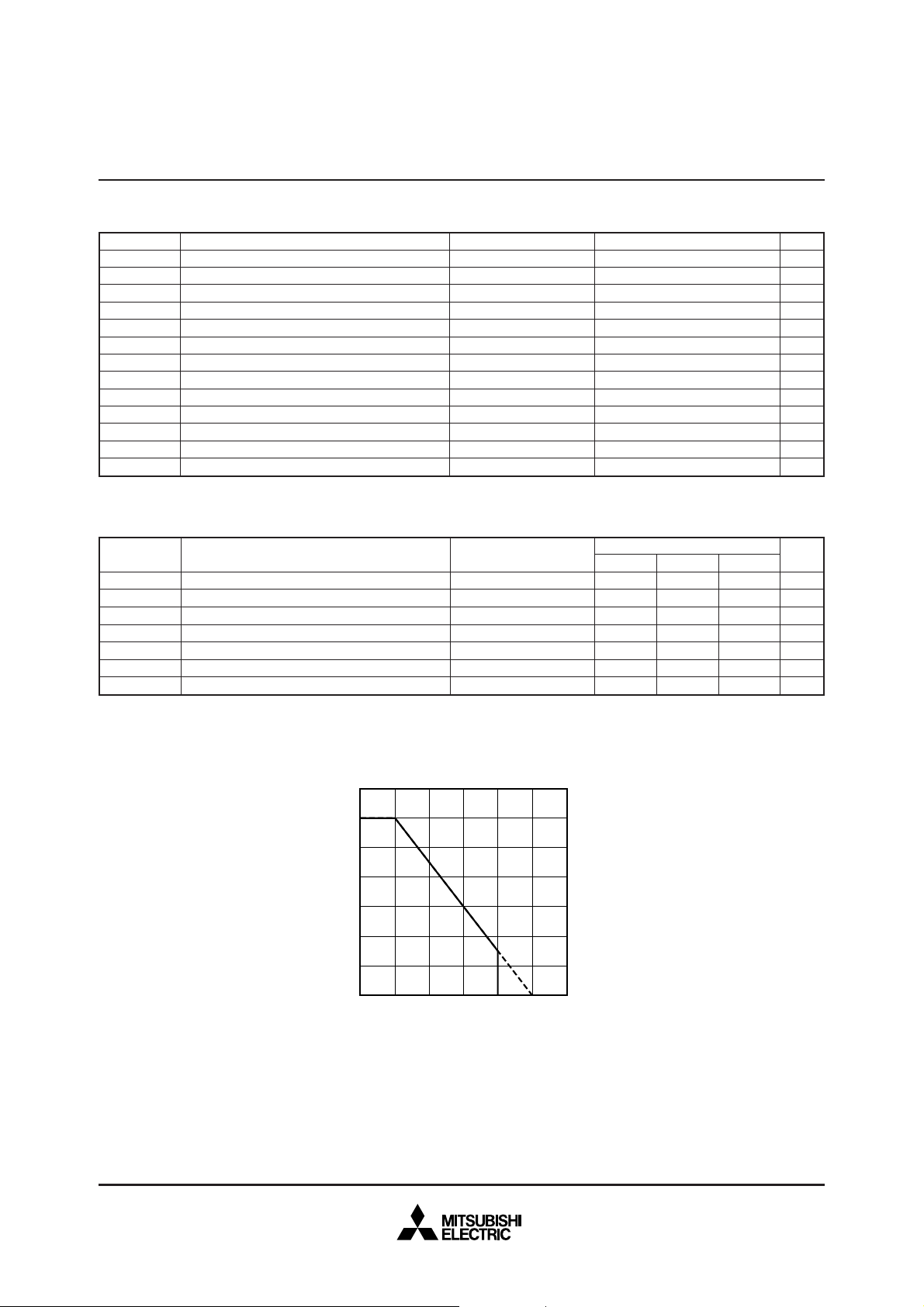
THERMAL DERATING FACTOR CHARACTERISTIC (MAXIMUM RATING)
0.7
0.6
0.5
0.4
0.3
0.2
0.1
Package Power Dissipation Pd (W)
0
0
25 50 10075 125 150
Temperature Ta (°C)
Mar. 2006

MITSUBISHI SEMICONDUCTORS <HVIC>
PRELIMINARY
Notice: This is not a final specification.
Some parametric limits are subject to change.
ELECTRICAL CHARACTERISTICS (Ta = 25°C, VCC = VBS ( = VB–VS) = 15V, unless otherwise specified)
Symbol UnitParameter Test conditions
V
FS
I
IBS
ICC
VOH
VOL
VIH
VIL
IIH
IIL
VBSuvr
VBSuvt
VBSuvh
tVBSuv
VCCuvr
VCCuvt
VCCuvh
tVCCuv
IOH
IOL
ROH
ROL
tdLH(HO)
tdHL(HO)
trH
tfH
tdLH(LO)
tdHL(LO)
trL
tfL
∆tdLH
∆tdHL
tinon
tinoff
∆P
WIO
* Typ. is not specified.
** It is recommended not to input short pulse continuously.
Floating Supply Leakage Current
BS Standby Current
V
CC Standby Current
V
High Level Output Voltage
Low Level Output Voltage
High Level Input Threshold Voltage
Low Level Input Threshold Voltage
High Level Input Bias Current
Low Level Input Bias Current
BS Supply UV Reset Voltage
V
BS Supply UV Trip Voltage
V
BS Supply UV Hysteresis Voltage
V
BS Supply UV Filter Time
V
CC Supply UV Reset Voltage
V
CC Supply UV Trip Voltage
V
CC Supply UV Hysteresis Voltage
V
CC Supply UV Filter Time
V
Output High Level Short Circuit Pulsed Current
Output Low Level Short Circuit Pulsed Current
Output High Level On Resistance
Output Low Level On Resistance
High Side Turn-On Propagation Delay
High Side Turn-Off Propagation Delay
High Side Turn-On Rise Time
High Side Turn-Off Fall Time
Low Side Turn-On Propagation Delay
Low Side Turn-Off Propagation Delay
Low Side Turn-On Rise Time
Low Side Turn-Off Fall Time
Delay Matching, High Side and Low Side Turn-On
Delay Matching, High Side and Low Side Turn-Off
Input Filter Time (ON)
Input Filter Time (OFF)
I/O Pulse Width Difference
B = VS = 600V
= LIN = 0V
HIN
= LIN = 0V
HIN
O = –20mA, LO, HO
I
O = 20mA, LO, HO
I
HIN, LIN
HIN, LIN
IN = 5V
V
IN = 0V
V
V
O = 0V, VIN = 5V, PW < 10µs**
O = 15V, VIN = 0V, PW < 10µs**
V
O = –20mA, ROH = (VOH–VO)/IO
I
IO = 20mA, ROL = VO/IO
CL = 1000pF between HO-VS
CL = 1000pF between HO-VS
CL = 1000pF between HO-VS
CL = 1000pF between HO-VS
CL = 1000pF between LO-GND
= 1000pF between LO-GND
CL
= 1000pF between LO-GND
CL
= 1000pF between LO-GND
CL
dLH(HO)–tdLH(LO)|
|t
dHL(HO)–tdHL(LO)|
|t
CONVEX PULSE
CONCAVE PULSE
CONVEX PULSE
CONCAVE PULSE
W(IN)–PW(OUT)|
|P
HIGH VOLTAGE HALF BRIDGE DRIVER
Limits
Min. Typ.* Max.
—
—
0.2
13.6
—
2.7
—
—
—
8.0
7.4
0.4
—
8.0
7.4
0.4
—
120
250
—
—
—
—
—
—
—
—
—
—
—
—
60
110
60
110
—
0.2
0.6
14.2
0.3
8.9
8.2
0.6
7.5
8.9
8.2
0.6
7.5
200
350
250
250
130
250
250
130
150
150
M81719FP
—
—
—
5
—
40
15
50
50
0
0
80
80
—
1.0
0.5
1.0
—
0.6
—
0.8
20
2
9.8
9.0
—
—
9.8
9.0
—
—
—
—
70
30
350
350
220
80
350
350
220
80
30
30
100
190
100
190
100
µA
mA
mA
V
V
V
V
µA
µA
V
V
V
µs
V
V
V
µs
mA
mA
Ω
Ω
ns
ns
ns
ns
ns
ns
ns
ns
ns
ns
ns
ns
ns
ns
ns
Mar. 2006

PRELIMINARY
Notice: This is not a final specification.
Some parametric limits are subject to change.
TIMING REQUIREMENT
IN
MITSUBISHI SEMICONDUCTORS <HVIC>
M81719FP
HIGH VOLTAGE HALF BRIDGE DRIVER
50% 50%
OUT
dLH
t
10% 10%
t
r
90% 90%
t
dHL
t
f
FUNCTION TABLE (X: H or L)
HIN Behavioral state
L
L
H
H
X
X
L
H
Note : “L” state of VBS UV, VCC UV means that UV trip voltage.
LIN VBS UV VCC UV HO LO
L
H
L
H
L
H
X
X
H
H
H
H
L
L
H
H
H
H
H
H
H
H
L
L
L
L
H
H
L
L
L
L
LO = HO = Low
L
LO = High
H
HO = High
L
LO = HO = High
H
HO = Low, VBS UV tripped
L
H
LO = High, VBS UV tripped
L
LO = Low, VCC UV tripped
L
HO = LO = Low, VCC UV tripped
TIMING DIAGRAM
1.Input/Output Timing Diagram
HIGH ACTIVE (When input signal (HIN or LIN) is “H”, then output signal (HO or LO) is “H”.)
Because there is not interlock circuit, in the case of both input signals (HIN and LIN) are “H”, output signals (HO and LO)
become “H”.
HIN
LIN
HO
LO
Mar. 2006

PRELIMINARY
Notice: This is not a final specification.
Some parametric limits are subject to change.
2.VCC (VBS) Supply Under Voltage Lockout Timing Diagram
When V
CC Supply Voltage keeps lower UV Trip Voltage (VCCuvt = VCCuvr–VCCuvh) for VCC Supply UV Filter Time, output
signal becomes “L”. And then, when V
CC Supply Voltage is higher than UV Reset Voltage, output signal LO becomes
“H”.
V
CC
CCuvt
V
t
VCCuv
LO
LIN
MITSUBISHI SEMICONDUCTORS <HVIC>
M81719FP
HIGH VOLTAGE HALF BRIDGE DRIVER
V
CCuvh
V
CCuvr
When V
CC Supply Voltage keeps lower UV Trip Voltage (VCCuvt = VCCuvr–VCCuvh) for VCC Supply UV Filter Time, output
signal becomes “L”. And then, when V
signal HO becomes “H”.
V
BS(H)
LIN
(L)
V
CC
V
CCuvt
HO
HIN
When V
BS Supply Voltage keeps lower UV Trip Voltage (VBSuvt = VBSuvr–VBSuvh) for VBS Supply UV Filter Time, output
signal becomes “L”. And then, V
BS Supply Voltage is higher than UV Reset Voltage, output signal HO keeps “L” until
next input signal HIN is “H”.
CC Supply Voltage is higher than UV Reset Voltage, input signal (LIN) is L; output
V
CCuvh
V
t
VCCuv
CCuvr
V
HO
HIN
BS
V
BSuvt
t
VBSuv
V
BSuvh
V
BSuvr
Mar. 2006

PRELIMINARY
Notice: This is not a final specification.
Some parametric limits are subject to change.
3.Allowable Supply Voltage Transient
It is recommended that supplying V
ting off V
BS firstly and shutting off VCC secondly. At the time of starting VCC and VBS, power supply should be increased
CC firstly and supplying VBS secondly. In the case of shutting off supply voltage, shut-
slowly. If it is increased rapidly, output signal (HO or LO) may be “H”.
Consideration
MITSUBISHI SEMICONDUCTORS <HVIC>
M81719FP
HIGH VOLTAGE HALF BRIDGE DRIVER
As for this product, the terminal of low voltage part and high-voltage part is very clear (The Fifth: LO, The Sixth: V
Therefore, pin insulation space distance should be taken enough.
PACKAGE OUTLINE
e
b
2
8
E
E
H
G
e
Z
1
5
1
e
Recommended Mount Pad
Dimension in Millimeters
41
D
z
Detail G
F
A
b
x
M
y
1
L
A
2
Detail F
A
1
L
c
Symbol
A
A
1
A
2
b
c
D
E
e
H
E
L
L
1
z
Z
1
x
y
b
2
e
1
I
2
Min Nom Max
––1.9
0.05 – –
–1.5–
0.35 0.4 0.5
0.13 0.15 0.2
4.8 5.0 5.2
4.2 4.4 4.6
–1.27–
5.9 6.2 6.5
0.2 0.4 0.6
–0.9–
–
0.595
–
–
––0.1
0° –10°
–0.76–
–5.72–
1.27 – –
2
I
–
–
0.745
–
0.25
S).
Mar. 2006
 Loading...