

Mitsubishi M5M5T5636UG-25, M5M5T5636UG-22, M5M5T5636UG-20 Datasheet

Advanced Information
M5M5T5636UG REV.0.2
M5M5T5636UG - 25
M5M5T5636UG - 22
M5M5T5636UG - 20
2001.July Rev.0.2
Advanced Information
Notice: This is not final specification.
Some parametric limits are subject to change.
MITSUBISHI LSIs
M5M5T5636UG – 25,22,20
18874368-BIT(524288-WORD BY 36-BIT) NETWORK SRAM
DESCRIPTION
The M5M5T5636UG is a family of 18M bit synchronous SRAMs
organized as 524288-words by 36-bit. It is designed to eliminate
dead bus cycles when turning the bus around between reads and
writes, or writes and reads. Mitsubishi's SRAMs are fabricated
with high performance, low power CMOS technology, providing
greater reliability. M5M5T5636UG operates on 2.5V power/ 1.8V
I/O supply or a single 2.5V power supply and are 2.5V CMOS
compatible.
FEATURES
• Fully registered inputs and outputs for pipelined operation
• Fast clock speed: 250, 225, and 200 MHz
• Fast access time: 2.6, 2.8, 3.2 ns
• Single 2.5V -5% and +5% power supply VDD
• Separate VDDQ for 2.5V or 1.8V I/O
• Individual byte write (BWa# - BWd#) controls may be tied
LOW
• Single Read/Write control pin (W#)
• CKE# pin to enable clock and suspend operations
• Internally self-timed, registers outputs eliminate the need to
control G#
• Snooze mode (ZZ) for power down
• Linear or Interleaved Burst Modes
• Three chip enables for simple depth expansion
• JTAG boundary scan support
APPLICATION
High-end networking products that require high bandwidth, such
as switches and routers.
FUNCTION
Synchronous circuitry allows for precise cycle control
triggered by a positive edge clock transition.
Synchronous signals include : all Addresses, all Data Inputs, all
Chip Enables (E1#, E2, E3#), Address Advance/Load (ADV),
Clock Enable (CKE#), Byte Write Enables (BWa#, BWb#, BWc#,
BWd#) and Read/Write (W#). Write operations are controlled by
the four Byte Write Enables (BWa# - BWd#) and Read/Write(W#)
inputs. All writes are conducted with on-chip synchronous selftimed write circuitry.
Asynchronous inputs include Output Enable (G#), Clock (CLK)
and Snooze Enable (ZZ). The HIGH input of ZZ pin puts the
SRAM in the power-down state.The Linear Burst order (LBO#) is
DC operated pin. LBO# pin will allow the choice of either an
interleaved burst, or a linear burst.
All read, write and deselect cycles are initiated by the ADV
LOW input. Subsequent burst address can be internally
generated as controlled by the ADV HIGH input.
Package
165(11x15) bump BGA
Body Size (13mm x 15mm)
Bump Pitch 1.0mm
PART NAME TABLE
Part Name Frequency Access Cycle
1
Active Current
(max.)
Standby Current
(max.)
250MHz 2.6ns 4.0ns 400mA 20mA
225MHz 2.8ns 4.4ns 380mA 20mA
200MHz 3.2ns 5.0ns 360mA 20mA
MITSUBISHI
ELECTRIC

Advanced Information
M5M5T5636UG REV.0.2
BUMP LAYOUT(TOP VIEW)
1 2 3 4 5 6 7 8 9 10 11
A NC A7 E1# BWc# BWb# E3# CKE# ADV A17 A8 NC
B NC A6 E2 BWd# BWa# CLK W# G# A18 A9 NC
C DQPc NC VDDQ VSS VSS VSS VSS VSS VDDQ NC DQPb
D DQc DQc VDDQ VDD VSS VSS VSS VDD VDDQ DQb DQb
E DQc DQc VDDQ VDD VSS VSS VSS VDD VDDQ DQb DQb
MITSUBISHI LSIs
M5M5T5636UG – 25,22,20
18874368-BIT(524288-WORD BY 36-BIT) NETWORK SRAM
165bump-BGA
F DQc DQc VDDQ VDD VSS VSS VSS VDD VDDQ DQb DQb
G DQc DQc VDDQ VDD VSS VSS VSS VDD VDDQ DQb DQb
H MCH MCH NC VDD VSS VSS VSS VDD NC NC ZZ
J DQd DQd VDDQ VDD VSS VSS VSS VDD VDDQ DQa DQa
K DQd DQd VDDQ VDD VSS VSS VSS VDD VDDQ DQa DQa
L DQd DQd VDDQ VDD VSS VSS VSS VDD VDDQ DQa DQa
M DQd DQd VDDQ VDD VSS VSS VSS VDD VDDQ DQa DQa
N DQPd NC VDDQ VSS NC NC MCH VSS VDDQ NC DQPa
P NC NC A5 A3 TDI A1 TDO A15 A13 A11 NC
R LBO# NC A4 A2 TMS A0 TCK A16 A14 A12 A10
Note1. MCH means "Must Connect High". MCH should be connected to HIGH.
2
MITSUBISHI
ELECTRIC
Advanced Information
M5M5T5636UG REV.0.2
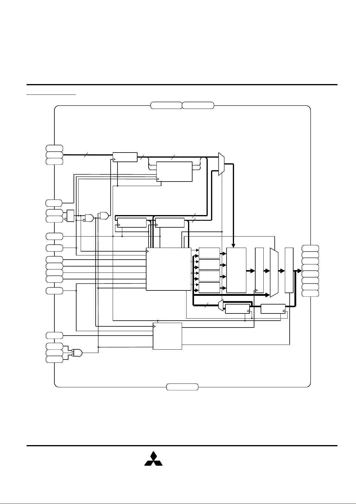
BLOCK DIAGRAM
DQa
LBO#
DQPa
DQb
DQPb
DQc
DQPc
DQd
DQPdA0A1
A2~18
CLK
CKE#ZZE2
E1#
E3#G#BWa#
BWb#
BWc#
BWd#
ADVW#VDD
VDDQ
VSS
MITSUBISHI LSIs
M5M5T5636UG – 25,22,20
18874368-BIT(524288-WORD BY 36-BIT) NETWORK SRAM
19
ADDRESS
REGISTER
WRITE ADDRESS
REGISTER1
19 17
A1
D1
LINEAR/
A0
INTERLEAVED
D0
BURST
COUNTER
WRITE ADDRESS
REGISTER2
WRITE REGISTRY
AND
DATA COHERENCY
CONTROL LOGIC
A1'
Q1
A0'
Q0
19
19
BYTE1
WRITE
DRIVERS
BYTE2
WRITE
DRIVERS
BYTE3
WRITE
DRIVERS
BYTE4
WRITE
DRIVERS
36
256Kx36
MEMORY
ARRAY
INPUT
REGISTER1
OUTPUT REGISTERS
OUTPUT SELECT
INPUT
REGISTER0
OUTPUT BUFFERS
READ
LOGIC
Note2. The BLOCK DIAGRAM does not include the Boundary Scan logic. See Boundary Scan chapter.
Note3. The BLOCK DIAGRAM illustrates simplified device operation. See TRUTH TABLE, PIN FUNCTION
and timing diagrams for detailed information.
3
MITSUBISHI
ELECTRIC

Advanced Information
M5M5T5636UG REV.0.2
PIN FUNCTION
DQa,DQPa,DQb,DQPb
DQc,DQPc,DQd,DQPd
Pin Name Function
A0~A18
BWa#, BWb#,
BWc#, BWd#
CLK Clock Input
E1#
Synchronous
Address
Inputs
Synchronous
Byte Write
Enables
Synchronous
Chip Enable
MITSUBISHI LSIs
M5M5T5636UG – 25,22,20
18874368-BIT(524288-WORD BY 36-BIT) NETWORK SRAM
These inputs are registered and must meet the setup and hold times around the rising edge of CLK.
A0 and A1 are the two least significant bits (LSB) of the address field and set the internal burst
counter if burst is desired.
These active LOW inputs allow individual bytes to be written when a WRITE cycle is active and
must meet the setup and hold times around the rising edge of CLK. BYTE WRITEs need to be
asserted on the same cycle as the address. BWs are associated with addresses and apply to
subsequent data. BWa# controls DQa, DQPa pins; BWb# controls DQb, DQPb pins; BWc# controls
DQc, DQPc pins; BWd# controls DQd, DQPd pins.
This signal registers the address, data, chip enables, byte write enables
and burst control inputs on its rising edge. All synchronous inputs must
meet setup and hold times around the clock's rising edge.
This active LOW input is used to enable the device and is sampled only when a new external
address is loaded (ADV is LOW).
E2
E3#
Synchronous
Chip Enable
Synchronous
Chip Enable
This active High input is used to enable the device and is sampled only when a new external
address is loaded (ADV is LOW). This input can be used for memory depth expansion.
This active Low input is used to enable the device and is sampled only when a new external
address is loaded (ADV is LOW). This input can be used for memory depth expansion.
G# Output Enable This active LOW asynchronous input enable the data I/O output drivers.
ADV
CKE#
ZZ
W#
LBO#
Synchronous
Address
Advance/Load
Synchronous
Clock Enable
Snooze
Enable
Synchronous
Read/Write
Synchronous
Data I/O
Burst Mode
Control
When HIGH, this input is used to advance the internal burst counter, controlling burst access after
the external address is loaded. When HIGH, W# is ignored. A LOW on this pin permits a new
address to be loaded at CLK rising edge.
This active LOW input permits CLK to propagate throughout the device. When HIGH, the device
ignores the CLK input and effectively internally extends the previous CLK cycle. This input must
meet setup and hold times around the rising edge of CLK.
This active HIGH asynchronous input causes the device to enter a low-power standby mode in
which all data in the memory array is retained. When active, all other inputs are ignored. When this
pin is LOW or NC, the SRAM normally operates.
This active input determines the cycle type when ADV is LOW. This is the only means for
determining READs and WRITEs. READ cycles may not be converted into WRITEs (and vice
versa) other than by loading a new address. A LOW on the pin permits BYTE WRITE operations
and must meet the setup and hold times around the rising edge of CLK. Full bus width WRITEs
occur if all byte write enables are LOW.
Byte “a” is DQa , DQPa pins; Byte “b” is DQb, DQPb pins; Byte “c” is DQc, DQPc pins; Byte “d” is
DQd,DQPd pins. Input data must meet setup and hold times around CLK rising edge.
This DC operated pin allows the choice of either an interleaved burst or a linear burst. If this pin is
HIGH or NC, an interleaved burst occurs. When this pin is LOW, a linear burst occurs, and input
leak current to this pin.
VDD VDD Core Power Supply
VSS VSS Ground
VDDQ VDDQ I/O buffer Power supply
TDI Test Data Input
TDO Test Data Output
TCK Test Clock
These pins are used for Boundary Scan Test.
TMS Test Mode Select
MCH Must Connect High These pins should be connected to HIGH
NC No Connect These pins are not internally connected and may be connected to ground.
4
MITSUBISHI
ELECTRIC

MITSUBISHI LSIs
Advanced Information
M5M5T5636UG REV.0.2
M5M5T5636UG – 25,22,20
18874368-BIT(524288-WORD BY 36-BIT) NETWORK SRAM
DC OPERATED TRUTH TABLE
Name Input Status Operation
LBO#
Note4. LBO# is DC operated pin.
Note5. NC means No Connection.
Note6. See BURST SEQUENCE TABLE about interleaved and Linear Burst Sequence.
BURST SEQUENCE TABLE
Interleaved Burst Sequence (when LBO# = HIGH or NC)
First access, latch external address A18~A2 0 , 0
Second access(first burst address) latched A18~A2 0 , 1
Third access(second burst address) latched A18~A2 1 , 0
Fourth access(third burst address) latched A18~A2 1 , 1
Linear Burst Sequence (when LBO# = LOW)
Operation A18~A2 A1,A0
First access, latch external address A18~A2 0 , 0 0 , 1 1 , 0 1 , 1
Second access(first burst address) latched A18~A2 0 , 1 1 , 0 1 , 1 0 , 0
Third access(second burst address) latched A18~A2 1 , 0 1 , 1 0 , 0 0 , 1
Fourth access(third burst address) latched A18~A2 1 , 1 0 , 0 0 , 1 1 , 0
Note7. The burst sequence wraps around to its initial state upon completion.
HIGH or NC Interleaved Burst Sequence
LOW Linear Burst Sequence
Operation A18~A2 A1,A0
0 , 1 1 , 0
0 , 0 1 , 1
1 , 1 0 , 0
1 , 0 0 , 1
1 , 1
1 , 0
0 , 1
0 , 0
TRUTH TABLE
E1# E2 E3# ZZ ADV W# BWx# G# CKE# CLK DQ
H X X L L X X X L L->H High-Z None Deselect Cycle
X L X L L X X X L L->H High-Z None Deselect Cycle
X X H L L X X X L L->H High-Z None Deselect Cycle
X X X L H X X X L L->H High-Z None Continue Deselect Cycle
L H L L L H X L L L->H Q External Read Cycle, Begin Burst
X X X L H X X L L L->H Q Next Read Cycle, Continue Burst
L H L L L H X H L L->H High-Z External NOP/Dummy Read, Begin Burst
X X X L H X X H L L->H High-Z Next Dummy Read, Continue Burst
L H L L L L L X L L->H D External Write Cycle, Begin Burst
X X X L H X L X L L->H D Next Write Cycle, Continue Burst
L H L L L L H X L L->H High-Z None NOP/Write Abort, Begin Burst
X X X L H X H X L L->H High-Z Next Write Abort, Continue Burst
X X X L X X X X H L->H - Current Ignore Clock edge, Stall
X X X H X X X X X X High-Z None Snooze Mode
Note8. X means "don't care". H means logic HIGH. L means logic LOW.
Note9. BWx#=H means all Synchronous Byte Write Enables (BWa#,BWb#,BWc#,BWd#) are HIGH. BWx#=L means one or more
Synchronous Byte Write Enables are LOW.
Note10. All inputs except G# and ZZ must meet setup and hold times around the rising edge (LOW to HIGH) of CLK.
5
Address
used
Operation
MITSUBISHI
ELECTRIC

Advanced Information
M5M5T5636UG REV.0.2
STATE DIAGRAM
Burst
Burst
Burst
Burst
MITSUBISHI LSIs
M5M5T5636UG – 25,22,20
18874368-BIT(524288-WORD BY 36-BIT) NETWORK SRAM
F , L , X
Deselect
T , L , H
X , H , X
F , L , X
T , L , H
Continue
Key
Read
Begin
Read
T , L , H
X , H , X
T , L , L
X , H , X
T , L , L
T , L , H
T , L , H
Input Command Code
T , L , L
F , L , X
Write
Begin
X , H , X T , L , L
Write
Continue
T , L , L
X , H , X
Transition
f
Next StateCurrent State
Note11. The notation "x , x , x" controlling the state transitions above indicate the state of inputs E, ADV and W# respectively.
Note12. If (E1# = L and E2 = H and E3# = L) then E="T" else E="F".
Note13. "H" = input "high"; "L" = input "low"; "X" = input "don't care"; "T" = input "true"; "F" = input "false".
6
MITSUBISHI
ELECTRIC

MITSUBISHI LSIs
Advanced Information
M5M5T5636UG REV.0.2
M5M5T5636UG – 25,22,20
18874368-BIT(524288-WORD BY 36-BIT) NETWORK SRAM
WRITE TRUTH TABLE
W# BWa# BWb# BWc# BWd# Function
H X X X X Read
L L H H H Write Byte a
L H L H H Write Byte b
L H H L H Write Byte c
L H H H L Write Byte d
L L L L L Write All Bytes
L H H H H Write Abort/NOP
Note14.X means "don't care". H means logic HIGH. L means logic LOW.
Note15. All inputs except G# and ZZ must meet setup and hold times around the rising edge (LOW to HIGH) of CLK.
ABSOLUTE MAXIMUM RATINGS
Symbol Parameter Conditions Ratings Unit
VDD Power Supply Voltage -1.0*~3.6 V
VDDQ I/O Buffer Power Supply Voltage -1.0*~3.6 V
VI Input Voltage -1.0~VDDQ+1.0** V
VO Output Voltage
PD Maximum Power Dissipation (VDD) 1050 mW
TOPR Operating Temperature 0~70 °C
TSTG(bias) Storage Temperature(bias) -10~85 °C
TSTG Storage Temperature -65~150 °C
Note16.* This is –1.0V when pulse width≤2ns, and –0.5V in case of DC.
** This is –1.0V~VDDQ+1.0V when pulse width≤2ns, and –0.5V~VDDQ+0.5V in case of DC.
With respect to VSS
-1.0~VDDQ+1.0** V
7
MITSUBISHI
ELECTRIC
 Loading...