

Mitsubishi M5M564R16DTP-12, M5M564R16DTP-10, M5M564R16DJ-15, M5M564R16DJ-12, M5M564R16DJ-10 Datasheet
1998.6.18 Ver.A
PRELIMINARY
Notice: This is not a final specification.
Some parametric limits are subject to change.
DESCRIPTION
The M5M564R16D is a family of 65536-word by 16-bit
static RAMs, fabricated with the high performance CMOS
process and designed for high speed application. These
devices operate on a single 3.3V supply, and are directly
TTL compatible.
They include a power down feature as well. In write
and read cycles, the lower and upper bytes are able
to be controled either togethe or separately by LB
and UB.
FEATURES
•Fast access time M5M564R16DJ,TP-10 ... 10ns(max)
M5M564R16DJ,TP-12 ... 12ns(max)
M5M564R16DJ,TP-15 ... 15ns(max)
•Low power dissipation Active .................. 363mW(typ)
•Single +3.3V power supply
•Fully static operation : No clocks, No refresh
•Common data I/O
•Easy memory expansion by S
•Three-state outputs : OR-tie capability
•OE prevents data contention in the I/O bus
•Directly TTL compatible : All inputs and outputs
•Separate control of lower and upper bytes by LB and UB
1048576-BIT (65536-WORD BY 16-BIT) CMOS STATIC RAM
MITSUBISHI LSIs
M5M564R16DJ,TP-10,-12,-15
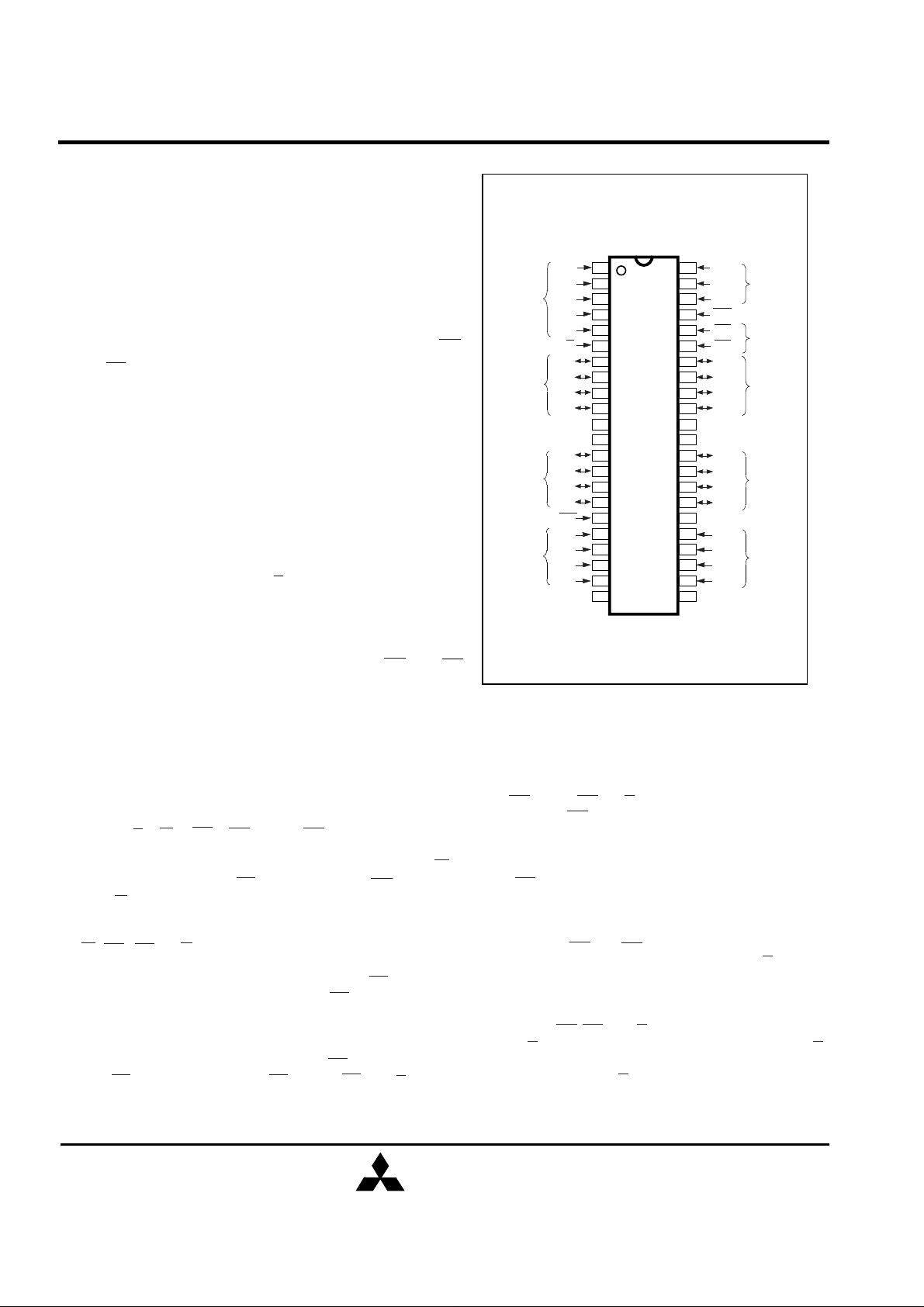
PIN CONFIGURATION (TOP VIEW)
44
A15
ADDRESS
A14
43
A13
42
OE
41
40
UB
LB
39
M5M564R16DJ,TP
38
DQ16
37
DQ15
36
DQ14
DQ13
35
GND
34
33
VCC
32
DQ12
31
DQ11
DQ10
30
DQ9
29
N.C
28
A12
27
A11
26
A10
25
A9
24
N.CN.C
23
INPUTS
OUTPUT ENABLE
INPUT
BYTE
CONTROL
INPUTS
DATA
INPUTS/
OUTPUTS
(0V)
(3.3V)
DATA
INPUTS/
OUTPUTS
ADDRESS
INPUTS
ADDRESS
INPUTS
CHIP
SELECT
INPUTS
DATA
INPUTS/
OUTPUTS
(3.3V)
DATA
INPUTS/
OUTPUTS
WRITE
CONTROL
INPUT
ADDRESS
INPUTS
A0
1
A1
2
A2
3
A3
4
A4
5
S
W
A5
A6
A7
A8
6
7
8
9
10
11
12
13
14
15
16
17
18
19
20
21
22
(0V)
DQ1
DQ2
DQ3
DQ4
VCC
GND
DQ5
DQ6
DQ7
DQ8
Outline 44P0K(J)
44P3W-H(TP)
APPLICATION
High-speed memory system
PACKAGE
M5M564R16DJ
M5M564R16DTP
FUNCTION
The operation mode of the M5M564R16D is
determined by a combination of the device control
inputs S, W, OE, LB, and UB. Each mode is
summarized in the function table.
A write cycle is executed whenever the low level W
overlaps with low level LB and/or low level UB and low
level S. The address must be set-up before write cycle
and must be stable during the entire cycle.
The data is latched into a cell on the traling edge of
W, LB, UB or S, whichever occurs first, requiring the
set-up and hold time relative to these edge to be
maintained. The output enable input OE directly
controls the output stage. Setting the OE at a high level,
the output stage is in a high impedance state, and the
data bus contention problem in the write cycle is
eliminated.
A read cycle is excuted by setting W at a high level
and OE at a low level while LB and/or UB and S are in
an active
MITSUBISHI
ELECTRIC
state. (LB and/or UB=L, S=L)
When setting LB at a high level and other pins are in
an active state, upper-Byte are in a selectable mode
in which both reading and writing are enable, and
lower-Byte are in a non-selectable mode. And when
setting UB at a high level and other pins are in an
active state, lower-Byte are in a selectable mode in
which both reading and writing are enable, and upperByte are in a non-selectable mode.
When setting LB and UB at a high level or S at high
level, the chip is in a non-selectable mode in which
both reading and writing are disabled. In this mode,
the output stage is in a high-impedance state,
allowing OR-tie with other chips and memory
expansion by LB, UB and S.
Signal-S controls the power-down feature. When S
goes high, power dissapation is reduced extremely.
The access time from S is equivalent to the address
access time.
: 44pin 400mil SOJ
: 44pin 400mil TSOP(II)
1

FUNCTION TABLE
MITSUBISHI LSIs
M5M564R16DJ,TP-10,-12,-15
1048576-BIT (65536-WORD BY 16-BIT) CMOS STATIC RAM
W
LL
H Read cycle All Bytes
LLH
LL
H
LL
LX
LLX
L
H
X
L
H
XX
BLOCK DIAGRAM
A0
1
A1
2
A2
3
A3
ADDRESS
INPUTS
CHIP SELECT
INPUTS
WRITE
CONTROL INPUT
OUTPUT
ENABLE INPUT
UPPER BYTE
CONTROL INPUTS
LOWER BYTE
CONTROL INPUTS
A4
A5
A6
A7
A8
S
W
OE
UB
LB
4
5
18
19
20
21
6
17
41
40
39
OE
L
X
H
X
X
UB LB
L
L
L
H
L
L
H
L
X
H
X
ROW INPUT BUFFERS
Read cycle Upper Bytes
H
Read cycle Lower Bytes
Write cycle All Bytes
L
L
Write cycle Upper Bytes
H
Write cycle Lower Bytes
X
H
Output disable
Non selection Stand by
18
512
DECODERS
ROW ADDRESS
Mode
High-impedance Active
High-impedance
High-impedance
High-impedance
MEMORY ARRAY
512 ROWS
2048 COLUMNS
2048
COLUMN I/O CIRCUITS
COLUMN ADDRESS
DECODERS
14
COLUMN INPUT BUFFERS
25 26 27 42 4324 44
A15A14A13A12A11A10A9
DQ1~8 DQ9~16
D
OUT
D
OUT
D
IN
IN
D
OUT
D
OUT
High-impedance
D
IN
D
IN
High-impedanceD
High-impedance
High-impedance
OUTPUT
BUFFERS
DATA
INPUT
BUFFERS
OUTPUT
BUFFERS
BUFFERS
DATA INPUT
IccS
Active
Active
Active
Active
Active
Active
7
DQ1
8
DQ2
9
DQ3
10
13
14
15
16
29
30
31
32
35
36
37
38
11
33
12
34
DQ4
DQ5
DQ6
DQ7
DQ8
DQ9
DQ10
DQ11
DQ12
DQ13
DQ14
DQ15
DQ16
V
CC
GND
DATA
INPUTS/
OUTPUTS
DATA
INPUTS/
OUTPUTS
(3.3V)
(0V)
ADDRESS INPUTS
MITSUBISHI
ELECTRIC
2

ABSOLUTE MAXIMUM RATINGS
MITSUBISHI LSIs
M5M564R16DJ,TP-10,-12,-15
1048576-BIT (65536-WORD BY 16-BIT) CMOS STATIC RAM
Symbol UnitConditions
cc
V
Supply voltage
VI
VO
d
P
Topr
Tstg(bias)
Output voltage
Power dissipation
Operating temperature
Storage temperature(bias)
Parameter
Input voltage
With respect to GND
Ta=25°C
Tstg
*Pulse width ≤5ns, In case of DC: - 0.5V
DC ELECTRICAL CHARACTERISTICS
(Ta=0~70°C, Vcc=3.3V ,unless otherwise noted)
Symbol Parameter
V
IH
High-level input voltage
V
VOH
VOL
I
I
ICC3
Low-level input voltage
IL
High-level output voltage
Low-level output voltage
I
Input current
I
I
OZ
Output current in off-state
Active supply current
CC1
(TTL level)
Stand-by supply current
CC2
(TTL level)
Stand-by current
(MOS level)
I
OH = - 4mA
OL= 8mA
I
= 0 ~ Vcc
I
V
VI (S)= VIH
VO= 0 ~ Vcc
VI (S)= VIL
other inputs VIH or VIL
Output-open(duty 100%)
VI (S)= VIH
VI (S)= Vcc - 0.2V
other inputs V
or V
I≥Vcc - 0.2V
I≤0.2V
Note 1: Direction for current flowing into an IC is positive (no mark).
CAPACITANCE
(Ta=0~70°C
, Vcc=3.3V ,unless otherwise noted)
+10%
-5%
Symbol Parameter
CI
CO
Note 2: C
Input capacitance
Output capacitance
I,CO are periodically sampled and are not 100% tested.
VI =GND,Vi =25mVrms,f=1MHz
o =GND,Vo =25mVrms,f=1MHz
V
Ratings
V
V
V
mW
°C
°C
°C
Min
2.0
Limits
MaxTyp
Vcc+0.3
Condition
*
- 2.0 ~ 4.6
*
- 2.0
~ Vcc+0.5
*
- 2.0 ~
1000
0 ~ 70
- 10 ~ 85
- 65 ~ 150Storage temperature
Vcc
+10%
-5%
0.8
2.4
0.4
AC(10ns cycle)
AC(12ns cycle)
AC(15ns cycle)
DC
AC(10ns cycle)
AC(12ns cycle)
AC(15ns cycle)
DC
110
200
195
190
140
70
65
60
40
10
Test Condition Unit
Limit
MaxTypMin
68pF
Unit
V
V
V
V
uA
2
2
uA
mA
mA
mA
pF
AC ELECTRICAL CHARACTERISTICS (Ta= 0~70 °C ,VCC=3.3V ,unless otherwise noted)
+10%
-5%
(1) MEASUREMENT CONDITION
Input pulse levels ................................... VIH=3.0V,VIL=0.0V
Input rise and fall time
Input timing reference levels
Output timing reference levels ................ VOH=1.5V, VOL=1.5V
Output loads
....................................................... Fig1 ,Fig2
................................................... 3ns
...................... VIH=1.5V,VIL=1.5V
OUTPUT
Z0=50Ω
RL=50Ω
VL=1.5V
Fig.1 Output load
DQ
DQ
Fig.2 Output load for t , t
255Ω
MITSUBISHI
ELECTRIC
5.0V
480Ω
5pF
Including
( )
scope and JIG
en dis
3
 Loading...