

Mitsubishi M5M51008CVP-70X, M5M51008CVP-70H, M5M51008CVP-55X, M5M51008CKV-70X, M5M51008CKV-70H Datasheet
...
MITSUBISHI LSIs
NC : NO CONNECTION
(max)
Active
(max)
stand-by
(max) Power supply current
The M5M51008CP,FP,VP,RV,KV,KR are a 1048576-bit CMOS
static RAM organized as 131072 word by 8-bit which are
fabricated using high-performance quadruple-polysilicon and
double metal CMOS technology. The use of thin film transistor
(TFT) load cells and CMOS periphery result in a high density and
low power static RAM.
They are low standby current and low operation current and ideal
for the battery back-up application.
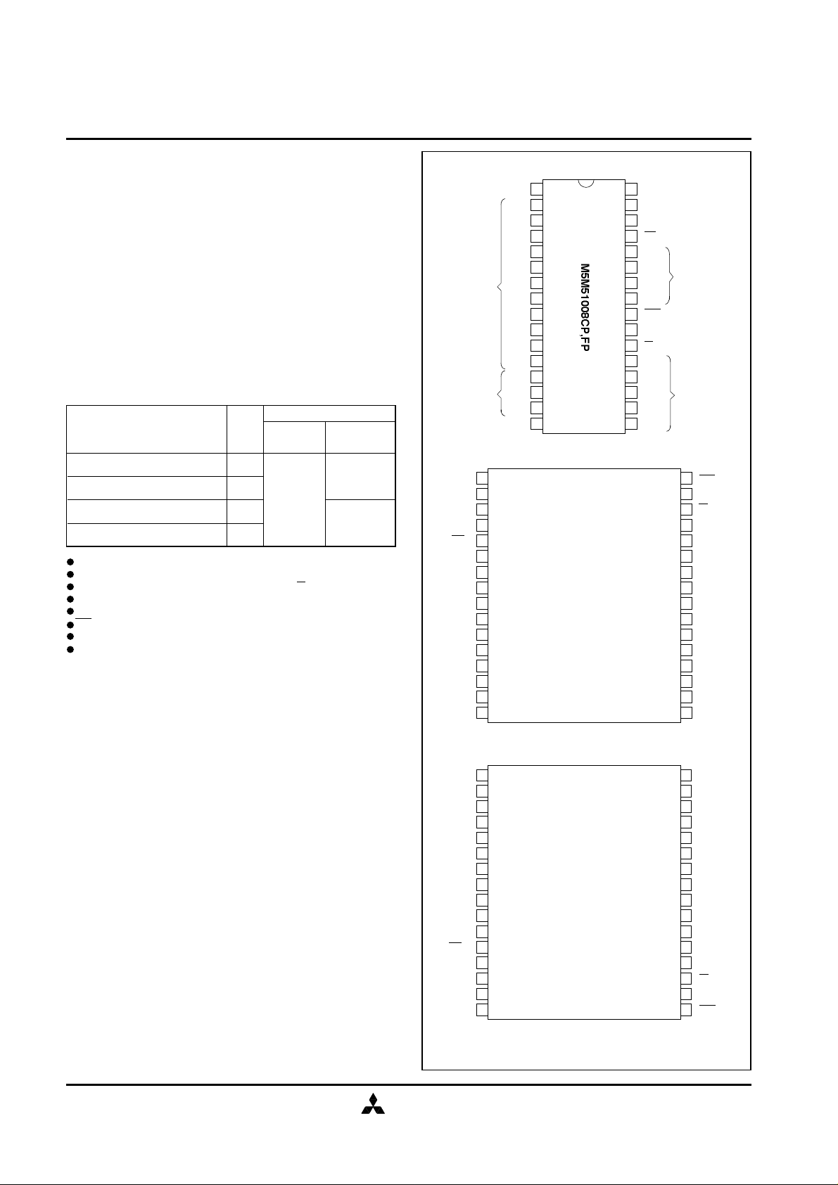
The M5M51008CVP,RV,KV,KR are packaged in a 32-pin thin
small outline package which is a high reliability and high density
surface mount device(SMD). Two types of devices are available.
M5M51008CVP,KV(normal lead bend type package),
M5M51008CRV,KR(reverse lead bend type package).Using both
types of devices, it becomes very easy to design a printed circuit
board.
M5M51008CP,FP,VP,RV,KV,KR-55H
8µA
(1MHz)
M5M51008CP,FP,VP,RV,KV,KR-70H
M5M51008CP,FP,VP,RV,KV,KR-55X
221615141311211109876543
2
123456789101112131415163231302928272625242322212019181712345678910111213141516323130292827262524232221201918171718192032
2122232425
2627282930
31
M5M51008CP,FP,VP,RV,KV,KR-70X
(Vcc=5.5V)
0.1µA
(Vcc=3.0V typ)
M5M51008CP,FP,VP,RV,KV,KR -55H, -70H,
-55X, -70X
1048576-BIT(131072-WORD BY 8-BIT)CMOS STATIC RAM
DESCRIPTION
FEATURES
Type name
Low stand-by current 0.1µA (typ.)
Directly TTL compatible : All inputs and outputs
Easy memory expansion and power down by S1,S2
Data hold on +2V power supply
Three-state outputs : OR - tie capability
OE prevents data contention in the I/O bus
Common data I/O
Package
M5M51008CP ············ 32pin 600mil DIP
M5M51008CFP ············ 32pin 525mil SOP
M5M51008CVP,RV ············ 32pin 8 X 20 mm TSOP
M5M51008CKV,KR ············ 32pin 8 X 13.4 mm TSOP
Access
time
55ns
70ns
55ns
70ns
15mA
(1MHz)
APPLICATION
Small capacity memory units
20µA
(Vcc=5.5V)
PIN CONFIGURATION (TOP VIEW)
NC
A16
A14
A12
A7
A6
ADDRESS
INPUTS
A5
A4
A3
A2
A1
A0
DQ1
DATA
INPUTS/
OUTPUTS
DQ2
DQ3
GND
Outline 32P4(P), 32P2M-A(FP)
A11
A9
A8
A13
W
S2
A15
VCC
M5M51008CVP,KV
NC
A16
A14
A12
A7
A6
A5
A4
Outline 32P3H-E(VP), 32P3K-B(KV)
VCC
ADDRESS
A15
INPUT
CHIP SELECT
S2
INPUT
WRITE CONTROL
W
INPUT
A13
A8
A9
A11
OUTPUT ENABLE
OE
INPUT
ADDRESS
A10
INPUT
CHIP SELECT
S1
INPUT
DQ8
DQ7
DQ6
DQ5
DQ4
ADDRESS
INPUTS
DATA
INPUTS/
OUTPUTS
OE
A10
S1
DQ8
DQ7
DQ6
DQ5
DQ4
GND
DQ3
DQ2
DQ1
A0
A1
A2
A3
MITSUBISHI
ELECTRIC
A4
A5
A6
A7
A12
A14
A16
NC
VCC
M5M51008CRV,KR
A15
S2
W
A13
A8
A9
A11
Outline 32P3H-F(RV), 32P3K-C(KR)
A3
A2
A1
A0
DQ1
DQ2
DQ3
GND
DQ4
DQ5
DQ6
DQ7
DQ8
S1
A10
OE
1
FUNCTION
The operation mode of the M5M51008C series are determined by
a combination of the device control inputs S1,S2,W and OE.
Each mode is summarized in the function table.
A write cycle is executed whenever the low level W overlaps with
the low level S1 and the high level S2. The address must be set up
before the write cycle and must be stable during the entire cycle.
The data is latched into a cell on the trailing edge of W,S1 or S2,
whichever occurs first,requiring the set-up and hold time relative to
these edge to be maintained. The output enable input OE directly
controls the output stage. Setting the OE at a high level, the output
stage is in a high-impedance state, and the data bus contention
problem in the write cycle is eliminated.
A read cycle is executed by setting W at a high level and OE at a
low level while S1 and S2 are in an active state(S1=L,S2=H).
at a low level, the chip are in
a non-selectable mode in which both reading and writing are
disabled. In this mode, the output stage is in a high- impedance
state, allowing OR-tie with other chips and memory expansion by
S1 and S2. The power supply current is reduced as low as the
stand-by current which is specified as ICC3 or ICC4, and the memory
data can be held at +2V power supply, enabling battery back-up
operation during power failure or power-down operation in the nonselected mode.
87654323128161514131211107412111092019181727262532121222325262728291314151718192021530632829223024321624A4A5A6A7A12
A14
A16
A15
A13A0A1A2A3A8A9
A11
DQ1
DQ2
DQ3
DQ4
DQ5
DQ6
DQ7
DQ8WS1S2OE
VCC
* Pin numbers inside dotted line show those of TSOP
*
*
2331A10
FUNCTION TABLE
S1 S2 W OE
X L X X
H X X X
L H L X
LLHHHHL
H
Mode DQ ICC
Non selection
High-impedance
Non selection High-impedance
Write
Read
Din
Dout
High-impedance
MITSUBISHI LSIs
M5M51008CP,FP,VP,RV,KV,KR -55H, -70H,
-55X, -70X
1048576-BIT(131072-WORD BY 8-BIT)CMOS STATIC RAM
When setting S1 at a high level or S2
Stand-by
Stand-by
Active
Active
Active
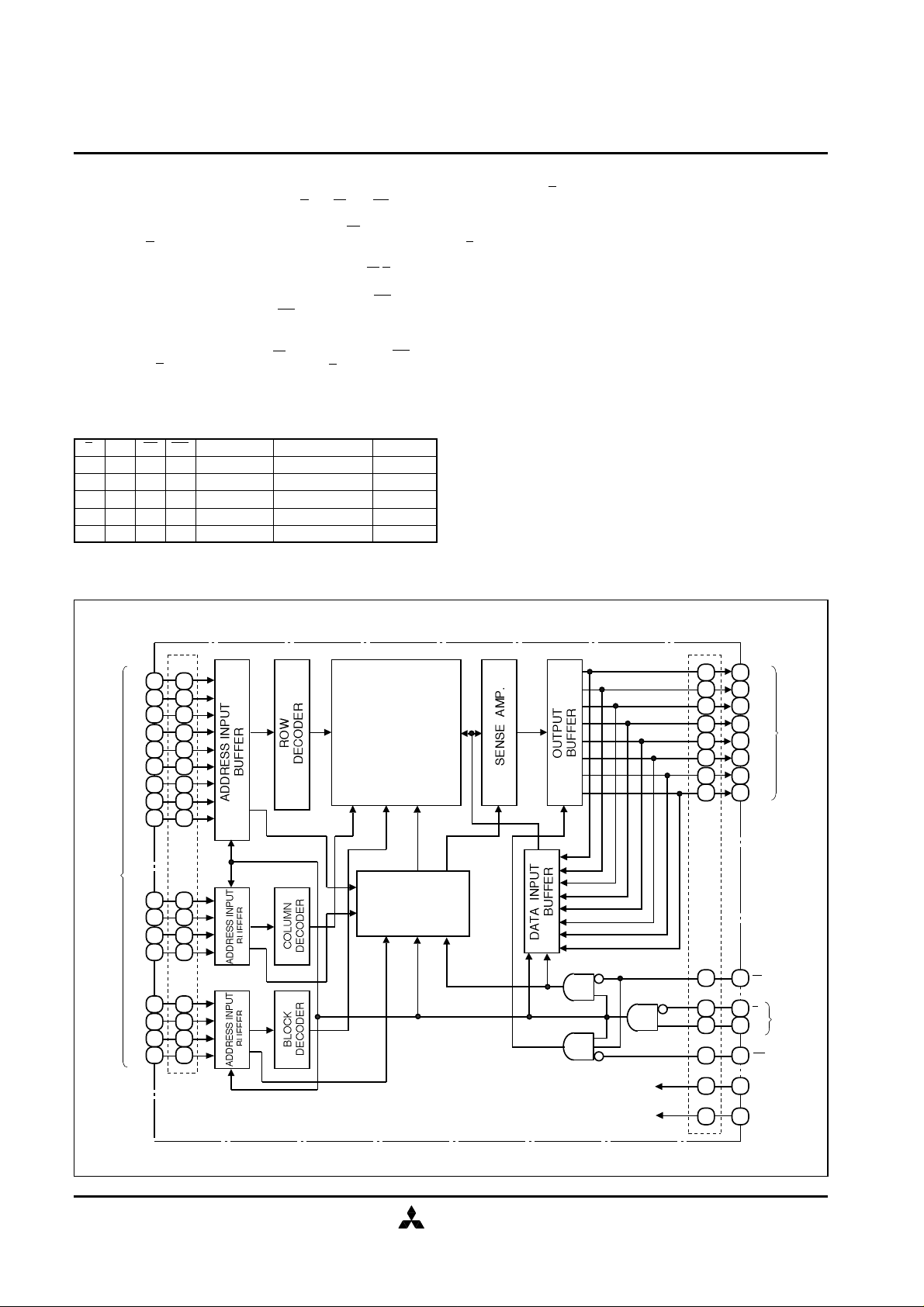
BLOCK DIAGRAM
ADDRESS
INPUTS
131072 WORDS
X 8 BITS
(512 ROWS
X128 COLUMNS
X 16BLOCKS)
CLOCK
GENERATOR
DATA
INPUTS/
OUTPUTS
WRITE
CONTROL
INPUT
CHIP
SELECT
INPUTS
OUTPUT
ENABLE
INPUT
MITSUBISHI
ELECTRIC
GND
(0V)
2
ABSOLUTE MAXIMUM RATINGS
IVOPdToprTstg
DC ELECTRICAL CHARACTERISTICS
* –3.0V in case of AC ( Pulse width ≤ 50ns )
Note 1: Direction for current flowing into an IC is positive (no mark).
2: Typical value is Vcc = 5V, Ta = 25°C
Symbol
V
cc
V
Symbol Parameter
VIH
VIL
VOH
VOL
II
IO
ICC1
ICC2
ICC3
ICC4
* –3.0V in case of AC ( Pulse width ≤ 50ns )
Supply voltage
Input voltage
Output voltage
Power dissipation
Operating temperature
Storage temperature
High-level input voltage
Low-level input voltage
High-level output voltage
Low-level output voltage
Input current
Output current in off-state
Active supply current
(AC, MOS level)
Active supply current
(AC, TTL level)
Stand-by current
Stand-by current
Parameter
M5M51008CP,FP,VP,RV,KV,KR -55H, -70H,
1048576-BIT(131072-WORD BY 8-BIT)CMOS STATIC RAM
Conditions
With respect to GND
Ta=25°C
(Ta=0~70°C, Vcc=5V±10%, unless otherwise noted)
Test conditions
IOH= –1.0mA
IOH= –0.1mA
IOL=2mA
VI=0~Vcc
S1=VIH or S2=VIL or OE=VIH
VI/O=0~VCC
S1 ≤ VCC–0.2V, S2 ≥ VCC–0.2V
other inputs ≤ 0.2V or ≥ VCC–0.2V
Output-open(duty 100%)
S1=VIL,S2=VIH,
other inputs=VIH or VIL
Output-open(duty 100%)
1) S2 ≤ 0.2V,
other inputs=0~VCC
2) S1 ≥ VCC–0.2V,
S2 ≥ VCC–0.2V,
other inputs=0~VCC
S1=VIH or S2=VIL,
other inputs=0~VCC
-H
-X
1MHz
~25°C
~40°C
~70°C
~25°C
~40°C
~70°C
55ns
70ns
55ns
70ns
Min
2.2
–0.3*
2.4
Vcc – 0.5
MITSUBISHI LSIs
Ratings
– 0.3*~7
– 0.3*~Vcc + 0.3
0~Vcc
700
0~70
– 65~150
Limits
MaxTyp
Vcc + 0.3
±1
±1
-55X, -70X
Unit
V
V
V
mW
°C
°C
Unit
V
0.8
0.4
80
70
151MHz
85
70
15
2
6
20
1
3
8
3
V
V
V
V
µA
µA
mA
mA
µA
mA
CAPACITANCE
Symbol
CI
CO
(Ta=0~70°C, Vcc=5V±10% unless otherwise noted)
Parameter
Input capacitance
Output capacitance
Test conditions
VI=GND, VI=25mVrms, f=1MHz
VO=GND,VO=25mVrms, f=1MHz
MITSUBISHI
ELECTRIC
Min
Limits
Typ
Max
10
Unit
6
pF
pF
3

M5M51008CP,FP,VP,RV,KV,KR -55H, -70H,
Limits
Limits
990Ω
1.8kΩ
VCC
DQ
1048576-BIT(131072-WORD BY 8-BIT)CMOS STATIC RAM
AC ELECTRICAL CHARACTERISTICS (Ta=0~70°C, 5V±10% unless otherwise noted )
MITSUBISHI LSIs
-55X, -70X
(1) MEASUREMENT CONDITIONS
Input pulse level VIH=2.4V,VIL=0.6V (-70H,-70X)
VIH=3.0V,VIL=0.0V (-55H,-55X)
Input rise and fall time 5ns
Reference level VOH=VOL=1.5V
Output loads Fig.1, CL=30pF (-55H,-70H,-55X,-70X)
CL=5pF (for ten,tdis)
Transition is measured ± 500mV from steady
state voltage. (for ten,tdis)
...............
......
................
.....................
(2) READ CYCLE
Symbol Parameter
tCR
ta(A)
ta(S1)
ta(S2)
ta(OE)
tdis(S1)
tdis(S2)
tdis(OE)
ten(S1)
ten(S2)
ten(OE)
tV(A)
Read cycle time
Address access time
Chip select 1 access time
Chip select 2 access time
Output enable access time
Output disable time after S1 high
Output disable time after S2 low
Output disable time after OE high
Output enable time after S1 low
Output enable time after S2 high
Output enable time after OE low
Data valid time after address
-55H,-55X
Min Max
55
55
55
55
30
20
20
20
5
5
5
5
CL ( Including scope
and JIG )
Fig.1 Output load
-70H,-70X
Min Max
70
70
70
70
35
25
25
25
10
10
5
10
Unit
ns
ns
ns
ns
ns
ns
ns
ns
ns
ns
ns
ns
(3) WRITE CYCLE
Symbol Parameter
tCW
tw(W)
tsu(A)
tsu(A-WH)
tsu(S1)
tsu(S2)
tsu(D)
th(D)
trec(W)
tdis(W)
tdis(OE)
ten(W)
ten(OE)
Write cycle time
Write pulse width
Address setup time
Address setup time with respect to W
Chip select 1 setup time
Chip select 2 setup time
Data setup time
Data hold time
Write recovery time
Output disable time from W low
Output disable time from OE high
Output enable time from W high
Output enable time from OE low
MITSUBISHI
ELECTRIC
-55H,-55X
MaxMin
55
45
0
50
50
50
25
0
0
5
5
20
20
-70H,-70X
MaxMin
70
55
0
65
65
65
30
0
0
5
5
25
25
Unit
ns
ns
ns
ns
ns
ns
ns
ns
ns
ns
ns
ns
ns
4

(4) TIMING DIAGRAMS
(Note 3)
(Note 3)
(Note 3)
(Note 3)
(Note 3)
(Note 3)
(Note 3)
(Note 3)
(Note 3)
(Note 3)
W = "H" level
Read cycle
A0~16
MITSUBISHI LSIs
M5M51008CP,FP,VP,RV,KV,KR -55H, -70H,
-55X, -70X
1048576-BIT(131072-WORD BY 8-BIT)CMOS STATIC RAM
tCR
S1
S2
OE
DQ1~8
Write cycle (W control mode)
A0~16
ta(A)
ta (S1)
ta (S2)
ta (OE)
ten (OE)
ten (S1)
ten (S2)
tv (A)
tdis (S1)
tdis (S2)
tdis (OE)
DATA VALID
tCW
S1
S2
OE
W
DQ1~8
tsu (A)
tdis (OE)
tsu (S1)
tsu (S2)
tsu (A-WH)
tdis (W)
MITSUBISHI
ELECTRIC
tw (W)
DATA IN
STABLE
tsu (D)
trec (W)
ten(OE)
ten (W)
th (D)
5

Write cycle ( S1 control mode)
(Note 3)
(Note 3)
(Note 5)
(Note 3)
(Note 3)
(Note 4)
(Note 5)
(Note 3)
(Note 3)
(Note 4)
(Note 3)
(Note 3)
Note 3: Hatching indicates the state is "don't care".
4: Writing is executed while S2 high overlaps S1 and W low.
6: Don't apply inverted phase signal externally when DQ pin is output mode.
A0~16
MITSUBISHI LSIs
M5M51008CP,FP,VP,RV,KV,KR -55H, -70H,
-55X, -70X
1048576-BIT(131072-WORD BY 8-BIT)CMOS STATIC RAM
tCW
S1
S2
W
DQ1~8
Write cycle (S2 control mode)
A0~16
tsu (A)
tsu (S1)
tsu (D)
tCW
trec (W)
th (D)
DATA IN
STABLE
S1
S2
W
DQ1~8
tsu (S2) trec (W)tsu (A)
tsu (D)
th (D)
DATA IN
STABLE
5: When the falling edge of W is simultaneously or prior to the falling edge of S1
or rising edge of S2, the outputs are maintained in the high impedance state.
MITSUBISHI
ELECTRIC
6

POWER DOWN CHARACTERISTICS
Vcc(PD)
(1) ELECTRICAL CHARACTERISTICS
Symbol Parameter
VCC (PD)
VI (S1)
VI (S2)
ICC (PD)
Power down supply voltage
Chip select input S1
Chip select input S2
Power down supply current
M5M51008CP,FP,VP,RV,KV,KR -55H, -70H,
1048576-BIT(131072-WORD BY 8-BIT)CMOS STATIC RAM
(Ta=0~70°C, unless otherwise noted)
Test conditions Unit
2.2V≤Vcc(PD)
2V≤Vcc(PD)≤2.2V
4.5V≤Vcc(PD)
Vcc(PD)<4.5V
VCC = 3V
1) S2 ≤ 0.2V,
other inputs = 0~3V
2) S1 ≥ VCC–0.2V,
S2 ≥ VCC–0.2V
other inputs = 0~3V
-H
-X
~25°C
~40°C
~70°C
~25°C
~40°C
~70°C
Min
2.0
2.2
MITSUBISHI LSIs
-55X, -70X
Limits
MaxTyp
0.8
0.2
1
3
10
0.5
1.5
4
V
V
V
µA
(2) TIMING REQUIREMENTS (Ta=0~70°C, unless otherwise noted )
Symbol Parameter
tsu (PD)
trec (PD)
Power down set up time
Power down recovery time
(3) POWER DOWN CHARACTERISTICS
S1 control mode
VCC
t su (PD)
2.2V
S1
4.5V
S1 ≥ VCC – 0.2V
S2 control mode
VCC
S2
t su (PD)
4.5V
Test conditions Unit
4.5V
4.5V
t rec (PD)
t rec (PD)
Min
0
5
Limits
MaxTyp
ns
ms
2.2V
0.2V
S2 ≤ 0.2V
MITSUBISHI
ELECTRIC
0.2V
7
 Loading...