

Mitsubishi M5M4V16169DRT-15, M5M4V16169DRT-10, M5M4V16169DTP-7, M5M4V16169DTP-15, M5M4V16169DTP-10 Datasheet
...
M5M4V16169DTP/RT-7,-8,-10,-15
MITSUBISHI LSIs
This document is a preliminary Target Spec. and someof the contents are subject to change without notice.
DESCRIPTION
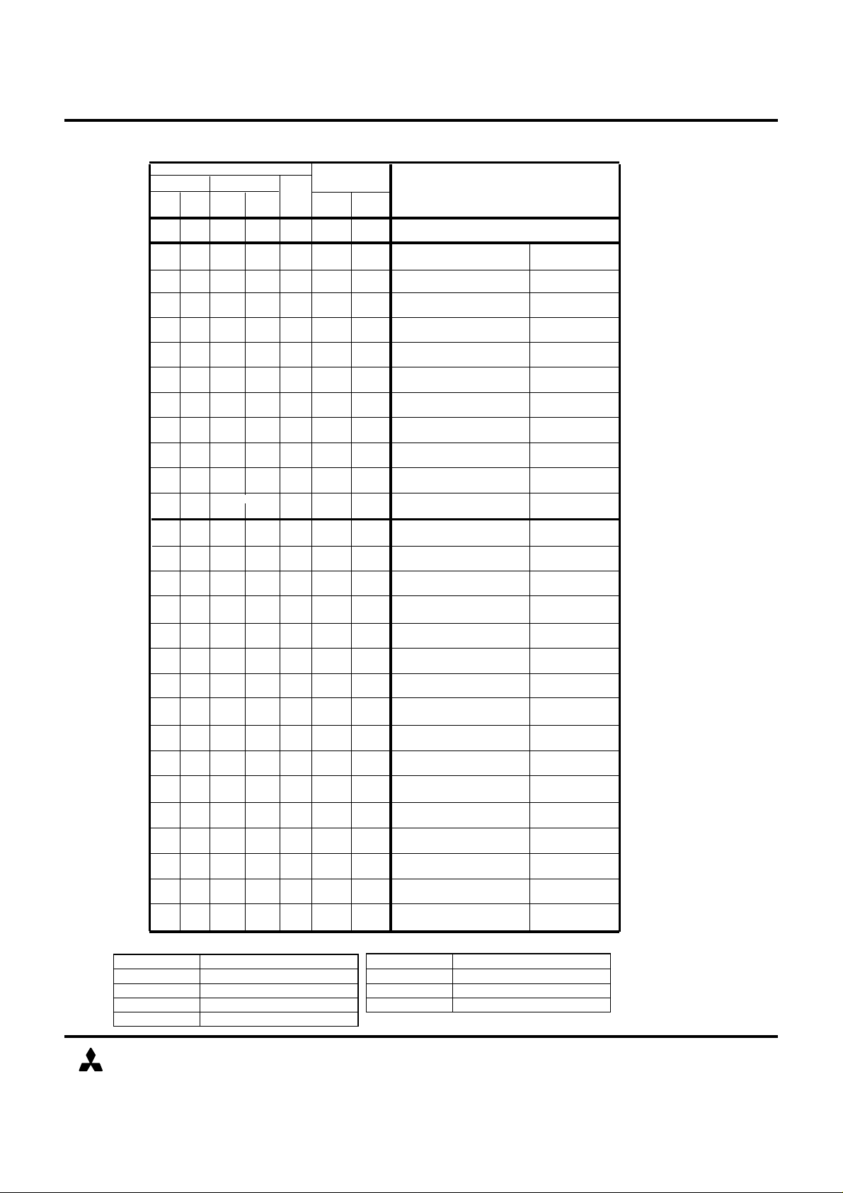
Vss
DQ9
As4
Ad6
Ad4
DQ13
As9
DQ11
VccQ
DQ10
Vss
DQ8G#As5
As3
Ad5
Ad3
ADF#
Vss
Vss
Ad9
Ad8
Ad7
Ad10
As8
As7
As6
DQ15
DQ14
VccQ
DQ12
Vcc
Vss
Vss
DQ6
As2
CAS#
Ad0
DQ2
CS#
DQ4
VccQ
DQ5
DQ7
MCH
As0
As1
RAS#
DTD#
Ad1
Ad2
Vcc
Vcc
DQCl
DQCu
CC1#
CC0#
WE#
CMd#
CMs#
K
DQ0
DQ1
VddQ
DQ3
Vss
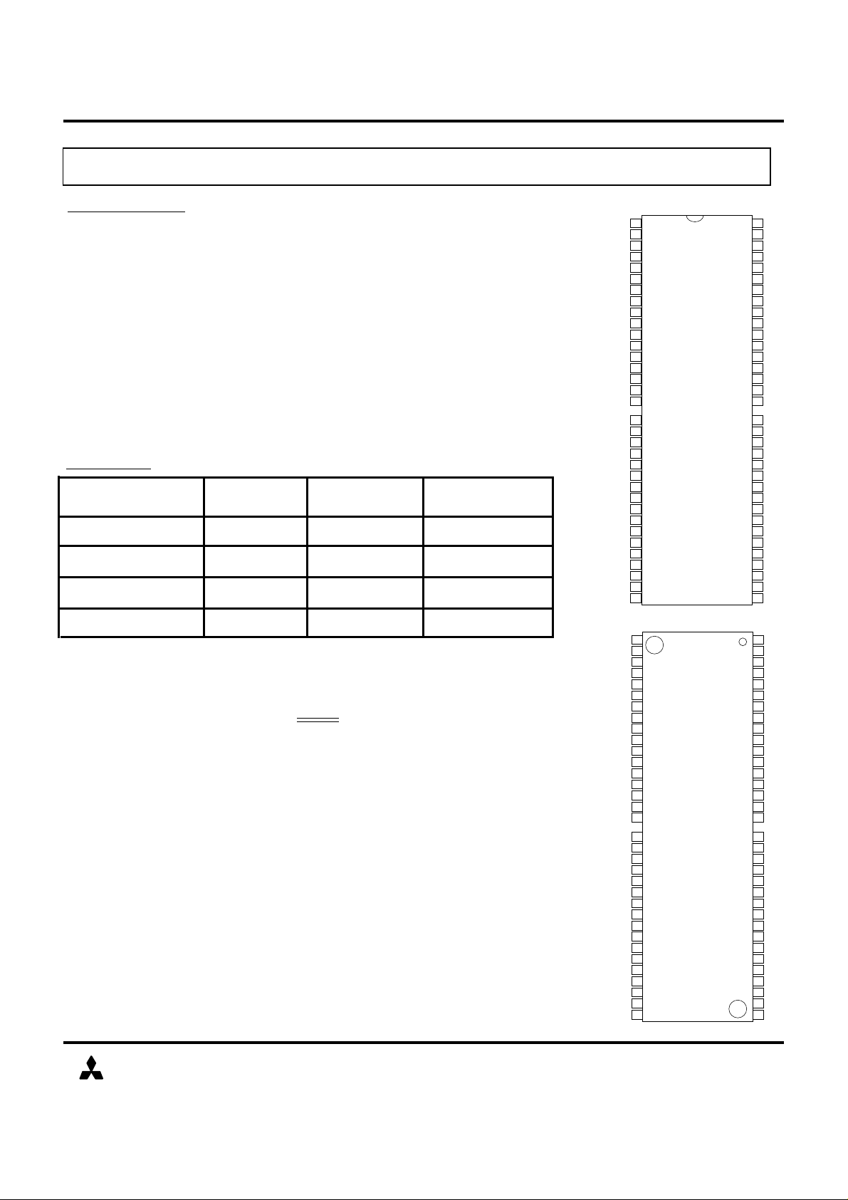
Package code:70P3S-L
Ad11
MCL
FEATURES
Power
Dissipation (Typ)
DRAM
Access/cycle
75ns/120ns
56ns/80ns
M5M4V16169TP/RT-15
6.4ns/8ns
SRAM: 800
SRAM: 420
M5M4V16169TP/RT-8
5.6ns/7ns
DRAM: 530
Vss
Vss
DQ6
As2
CAS#
Ad0
DQ2
CS#
DQ4
VccQ
DQ5
DQ7
MCH
As0
As1
RAS#
DTD#
Ad1
Ad2
Vcc
Vcc
DQCl
DQCu
CC1#
CC0#
WE#
CMd#
CMs#
K
DQ0
DQ1
VccQ
DQ3
Vss
Package code:70P3S-M
Vss
DQ9
As4
Ad6
Ad4
DQ13
As9
DQ11
VccQ
DQ10
Vss
DQ8G#As5
As3
Ad5
Ad3
ADF#
Vss
Vss
Ad9
Ad8
Ad7
Ad10
As8
As7
As6
DQ15
DQ14
VccQ
DQ12
Vcc
Ad11
MCL
PINCONFIGURATION
(TOP VIEW)
60ns/90ns
8.0ns/10ns
SRAM: 660
M5M4V16169TP/RT-10
16MCDRAM:16M(1M-WORD BY 16-BIT) CACHED DRAM WITH 16K (1024-WORD BY 16-BIT) SRAM
Preliminary
The M5M4V16169DTP/RT is a 16M-bit Cached DRAM which integrates input
1.
registers, a 1,048,576-word by 16-bit dynamic memory array and a 1024- word
by 16-bit static RAM array as a Cache memory (block size 8x16) onto a single
monolithic circuit. The block data transfer between the DRAM and the data
transfer buffers (RB1/RB2/WB1/WB2) is performed in one instruction cycle, a
fundamental advantage over a conventional DRAM/SRAM cache.
The RAM is fabricated with a high performance CMOS process, and is ideal for
large-capacity memory systems where high speed, low power dissipation, and
2.
low cost are essential. The use of quadruple-layer polysilicon process combined
with silicide and double layer aluminum wiring technology, a single-transistor
dynamic storage stacked capacitor cell, and a six-transistor static storage cache
cell provide high circuit density at reduced costs.
Type name
M5M4V16169TP/RT-7
SRAM
Access/cycle
8.0ns/15ns
# 70-pin,400-mil TSOP (type II ) with 0.65mm
lead pitch and 23.49mm package length.
# Multiplexed DRAM address inputs for reduced pin
count and higher system densities.
# Selectable output operation (transparent / latched /
registered) using set command register cycle.
# Single 3.3V +/- 0.3V Power Supply.
(3.3V +/- 0.15V for -7 part)
# 2048 refresh cycles every 64ms (Ad0->Ad10).
# Programmable burst length (1,2,4,8) and burst
sequence (sequential,interleave) with no latency.
# Synchronous design for precise control with
an external clock (K).
# Output retention by advanced mask clock (CMs#).
# All inputs/outputs low capacitance and LVTTL
compatible.
# Separate DRAM and SRAM address inputs
for fast SRAM access.
# Page Mode capability.
# Auto Refresh capability.
# Self Refresh capability.
49ns/70ns
K
CS#
CMd#
RAS#
CAS#
DTD#
Ad
CMs#
CC0#,CC1#
WE#
DQC(u/l)
As
G#
DQ
Vcc
VccQ
Vss
ADF#
MCL
MCH
SRAM: 860
DRAM: 500
DRAM: 430
DRAM: 330
: Master Clock
: Chip Select
: DRAM Clock Mask
: Row Addr. Strobe
: Column Addr. Strobe
: Data Transfer Direction
: DRAM Address
: SRAM Clock Mask
: Control Clocks
: Write Enable
: I/O Byte Control
: SRAM Address
: Output Enable
: Data I/O
: Power Supply
: DQ Power Supply
: Ground
:Address Fetch clock
This pin can be None-Connect.
:Must Connect Low
:Must Connect High
1
2
3
4
5
6
7
8
9
10
11
12
13
14
15
16
17
19
20
21
22
23
24
25
26
27
28
29
30
31
32
33
34
35
70
69
68
67
66
65
64
63
62
61
60
59
58
57
56
55
54
52
51
50
49
48
47
46
45
44
43
42
41
40
39
38
37
36
400 mil
70Pin
TSOP
Type II
0.65mm
Lead
Pitch
400 mil
70Pin
TSOP
Type II
0.65mm
Lead
Pitch
70
69
68
67
66
65
64
63
62
61
60
59
58
57
56
55
54
52
51
50
49
48
47
46
45
44
43
42
41
40
39
38
37
36
1
2
3
4
5
6
7
8
9
10
11
12
13
14
15
16
17
19
20
21
22
23
24
25
26
27
28
29
30
31
32
33
34
35
MITSUBISHI ELECTRIC
(REV 1.0) Jul. 1998
1
M5M4V16169DTP/RT-7,-8,-10,-15
MITSUBISHI LSIs
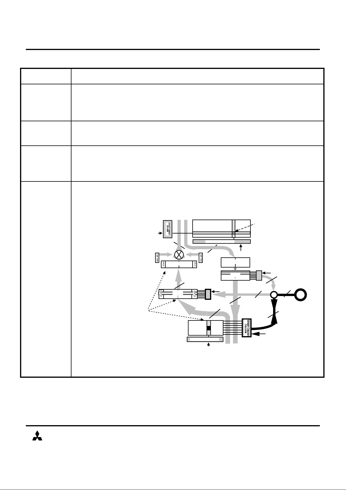
Buffer
1
0
7
16M DRAM
Mask
RB1
RB2
WB2
WB1
WB2M
WB1M
Ad10
Ad8
Ad2
Ad0
7
K
9
5
14
19
22
47
50
55
58
Ad4
SRAM
Address
input
16MCDRAM:16M(1M-WORD BY 16-BIT) CACHED DRAM WITH 16K (1024-WORD BY 16-BIT) SRAM
BLOCK DIAGRAM 1
Ad11
DRAM
Address
Input
66
65
69
Ad9
68
Ad7 67
Ad6
41
40
Ad5
39
Ad3 38
34
Ad1 33
32
64
As9
As8
63
62
As7
As6 61
As5 44
43
As4
42
As3
28
As2
As1 27
26
As0
Col.3-7
Row 0-11
Command (0-6)
WB2 Mask
WB1
As3-9
As0-2
Vcc
54 35 122348 59 701736 15 20 51 56
1
Vss
VccQ
Column Block Decoder
1M bit
DRAM
Array
Sense Amplifier and I/O control
0
Read Buffer1
Read Buffer2
Write Buffer 2
Write Buffer 1
021
S/A and I/O
Col.Decoder
1KBit
1
7
1Kx16=16K
2
16
SRAM
1M x 16=
7
Din
Main
Amp.
SRAM
Array
Mask
KBuffer
Timing
control
Mask
29
RAS#
(Row Address strobe)
30
CAS#
(Column Address strobe)
31
DTD#
(Data Transfer Direction)
CMd#8
(Clock Mask for DRAM)
CS#
(Chip Select)
10
(Master ClocK)
CMs#
(Clock Mask for SRAM)
6
WE#
(Write Enable)
CC0#
(Control Clock 0)
4
CC1#
(Control Clock 1)
ADF#37
(Address Fetch)
DQCu(Enable upper)
3
DQCl(Enable lower)
2
DQ011
13
DQ1
DQ2
16
DQ3
DQ4
21
DQ5
DQ6
24
DQ7
DQ8
49
DQ9
DQ10
52
DQ11
DQ12
57
DQ13
DQ14
DQ1560
45
G#
(Output Enable)
MITSUBISHI ELECTRIC
(REV 1.0) Jul. 1998
2
M5M4V16169DTP/RT-7,-8,-10,-15
MITSUBISHI LSIs
16MCDRAM:16M(1M-WORD BY 16-BIT) CACHED DRAM WITH 16K (1024-WORD BY 16-BIT) SRAM
BLOCK DIAGRAM 2
Ad3-7
1 of 32
Decode
8X16
WB2
DQ0-7 DQ8-15
WB1
Upper ByteLower Byte
8X16
Upper ByteLower Byte
DRAM
1MX16
DRAM Row Decoder
8X16
As0-2
1of8
Decode
RB1
Upper ByteLower Byte
RB2
Upper ByteLower Byte
Ad0-11
1 of 4096 Decode
16 bits
8X16 Block
As0-2
1of8Decode
16 bits
16 bits
DQs
8X16 Block
SRAM Row Decoder
MITSUBISHI ELECTRIC
8X16 8X16
SRAM
1KX16
As3 - 9
1 of 128 Decode
16 bits
As0-2
1of8Decode
(REV 1.0) Jul. 1998
3
M5M4V16169DTP/RT-7,-8,-10,-15
16MCDRAM:16M(1M-WORD BY 16-BIT) CACHED DRAM WITH 16K (1024-WORD BY 16-BIT) SRAM
Mnemonic
FUNCTION TRUTH TABLE
MITSUBISHI LSIs
(SRAM
As
address)
As0-9
Previous
CMd#
XX
CODE
NOP
CS#
H
Previous
CMs#
H X X X XXXX
SRAM
DQC
(u/l)
WE#CC0# CC1#
X X X X XX XX X XSPD L X
L X X X XH LH H XLBM H X
DES
SR
SW
BWT
BRTR
L X X X XXX XH H
H X
L X X X XAs0-9H HH LH X
L X X X XAs0-9H LH L
H X
L X X X XAs3-9L HL HBRT H X
L X X X XAs3-9L LL HH X
L X X X XAs0-9H HL H
H X
(2)
(2)
BWTW L X X X XAs0-9H LL HH X
BR
DPD
DNOP
DRT
DWT1
DWT1R
L X X X XAs0-2H HL L
H X
L X X X XAs0-2H LL LBW H X
X
X X X X XXXX X X L
L H H X XX X X X X
X H
L H L H
L H L L 0 0
L 0 0H L L
X X X X XX H 00 0
X X X X X
X H 0
X X X X X
X H 1
(2)
(2)
L 0 1
L 0 1
DWT3
DWT3R
L
L 1 0H L L
X X X X X
X H 1
X X X X X
X H 0
L 1 1
L 1 1
ACT
L L H H
X X X X X
X H
L L H L XX X X X XPCG X H
L L L H XX X X X XARF X H
L L L H XX X X X XSRF X H
DRAM
CAS#
RAS# DTD#
Ad (DRAM address)
Ad0-11
H
(1)
(1) (1)
Ad3-7
(Col.Block)
Ad3-7
(Col.Block)
Ad3-7
(Col.Block)
H L LX X X X XDWT2 X H 0
H L LX X X X XDWT2R X H 1
H L L
H L LX X X X XDWT4 X H 0
H L LX X X X XDWT4R X H 1
(7)
(8)
Ad3-7
(Col.Block)
Ad3-7
(Col.Block)
Ad3-7
(Col.Block)
Ad3-7
(Col.Block)
Ad3-7
(Col.Block)
Ad3-7
(Col.Block)
Ad0-11
(Row Add.)
Ad2
Ad1
Ad0
(2)
(2)
(2)
(2)
(2)
(2)
0
1
(2)
(2)
(2)
L L L L CommandX X X X XSCR X H
NOTES
1) For the DPD function, the RAS#, CAS# and DTD# inputs are
DON'T CARE except for the L,L,H combination. (Respectively).
2) The unused addresses must be set to Low.
3) Use New: If BW or BWT or BWTW is initiated the same cycle
as DWT1 or DWT1R, new data is loaded into the buffer
and transferred to DRAM.
4) Clear 1 or 2 Transfer Mask Bits (as addressed by As0-2 and DQCU/L).
5) Actual number of bits transfer depends on the state of the DTBW Mask and
6) Following a DWT1 or DWT1R cycle, the entire WB1 Transfer Mask is Set .
7) CMd# during current cycle must be High (see timing diagram for Auto-Refresh).
8) CMd# during current cycle must be Low (see timing diagram for Self-Refresh).
MITSUBISHI ELECTRIC
the DQCU/DQCL inputs. Note: If DQC(U/L) is Low, the corresponding DQ(s)
is(are) disabled (Input and Output Buffer). SR,SW,BR and BW cycles
with DQCU and DQCL Low result in a Deselect SRAM operation.
(i.e. , data can no longer be transferred from WB1 to DRAM.)
Succeeding Buffer-Writes or Buffer Write Transfers will Clear Mask bits.
(REV 1.0) Jul. 1998
4
M5M4V16169DTP/RT-7,-8,-10,-15
MITSUBISHI LSIs
Xfer Masks
Write Buffers
SRAM->DO
DIN->SRAM
RB2->SRAM
RB2->DO
DIN->WB1
DIN->SRAM->WB1
DRAM->RB1->RB2
WB1->WB2->DRAM
Use
Use
Load
Load
-----------
-
---
-
---
-
-
-
-
-
---
-----
---
-------
---
-------
---
-----
-----
-----
-
-
-
-
-
---
-
-
No operation
WB1->WB2->DRAM
->DRAM->RB1->RB2
WB2->DRAM
WB2->DRAM->RB
Use
Use
-
Use
-----
--------
-
-
-
16MCDRAM:16M(1M-WORD BY 16-BIT) CACHED DRAM WITH 16K (1024-WORD BY 16-BIT) SRAM
FUNCTION TRUTH TABLE
Data Transfer Buffers
WB1
WB1
WB2
Mask
WB2
Mask
Read
Buffer
RB1,2
DQ pin
Din
Dout
Function
-- - - -
-- - --
-- - - --
-
-
-
-
Load/
Use
Load/
Use
Use
Load/
Use
Load/
Use
Clear
Mask
Clear
Mask
Clear 1
or 2 bits
Use
Use
- -
(4)
-
-
(6)
(6)
Load
-
-
Use
Use
-
Suspend No operation
Byte
Hi-Z
mask
Hi-Z No operation
Valid
Valid Hi-Z
No OperationHi-Z
SRAM Power Down&
Data retention
DRAM Power Down
Deselect SRAM
SRAM Read
SRAM Write
Buffer Read XferUse Hi-Z
Buffer Write Xfer SRAM->WB1
- -
-
Use RB2->SRAM->DO
Use
Hi-Z
Valid
-
Valid Hi-Z
Valid
Buffer Read Xfer & Read
Buffer Read Xfer & Read
Buffer Read
Buffer WriteValid Hi-Z
-
-
-
-
-
-
DRAM Power Down
-
DRAM No OPeration
-
DRAM Read XferLoad
Load/
Use
Load/
Load DRAM Write Xfer1& Read
Use
Use
-
-
-
-
-
Load
Load
Load
Load
-
DRAM Write Xfer1
-
-
DRAM Write Xfer2 WB2->DRAM
-
DRAM Write Xfer2& Read
DRAM Write Xfer3
DRAM Write Xfer3& Read
DRAM Write Xfer4
No operation
No operation
WB1->WB2
->DRAM->RB1->RB2
WB2->DRAM
->RB1->RB2
WB1->WB2
(3)
(3)
(3)
Use
Load
DRAM Write Xfer4& Read
DRAM Activate
DRAM Precharge
Auto Refresh
Self Refresh Entry
Set Command Register
Function
Din --> SRAM
Din --> WB1
SRAM --> WB1
WB1 --> WB2
WB2 --> DRAM
Data Transferred (max)
8/16 bits
8/16bits
(5)
(5)
128 bits (8X16bit-block)
128 bits (8X16bit-block)
128 bits (8X16bit-block)
Function
WB2 --> RB
DRAM --> RB
RB --> Dout
RB --> SRAM
MITSUBISHI ELECTRIC 5
Page Call
Data Transferred (max)
128 bits (8X16bit-block)
128 bits (8X16bit-block)
8/16 bits
(5)
128 bits (8X16bit-block)
(REV 1.0) Jul. 1998
DO: Data Out
DIN: Data In
WB1: Write Buffer 1
WB2: Write Buffer 2
RB: Read Buffer
M5M4V16169DTP/RT-7,-8,-10,-15
MITSUBISHI LSIs
for
the CDRAM. All external timing parameters (with the exception of G# in read cycle
and CMd# in Self refresh cycle) are specified with respect to the rising edge of K.
(K).
When CMd# is Low at the rising edge of K, the internal DRAM master clock (K) for
the following cycle is ceased and input stages are powered-off, resulting in a DRAM
Power Down.
the
states of CMd#, CAS#, and DTD#) to activate the DRAM (latching the Row Address
lines and accessing 1 of 4096 rows), initiate a DRAM precharge cycle, perform a
DRAM Read or Write Transfer, DRAM Write Transfer & Read, set the command
registers, start an Auto-Refresh cycle, enter a Self-Refresh cycle,create a DRAM
NOP cycle, or power down the DRAM.
the
Column addresses. When preceded by RAS# in a DRAM access cycle, CAS#
initiates a DRAM Write Transfer (WB1/2 -> DRAM, if DTD#=L), DRAM Write
Transfer & Read (WB1/2 -> DRAM -> RB, if DTD#=L) or DRAM Read Transfer
(DRAM -> RB, if DTD#=H), depending on the state of DTD# (see DTD# pin
description).
(write)
direction. If preceded by a RAS# low cycle, both CAS# and DTD# low (on the
rising edge of K) initiate a DRAM Write Transfer cycle. If DTD# stays High with the
above conditions, a DRAM Read Transfer cycle results. DTD# can also initiate
DRAM Activate, DRAM Precharge, Auto-Refresh, Set-Command Register, and
Self Refresh cycles.
(@
RAS=low,CAS=high,DTD=high, K=Rising edge) specify the Row Address of the
DRAM to activate and refresh the selected page and Ad3-Ad7 (@
RAS=high,CAS=low,K=Rising edge) specify the Block Address of the DRAM. In
addition, Ad0-Ad2 (@ RAS=high,CAS=low, K=Rising edge) specify the transfer
operation of the DRAM . Also Ad0-Ad9 (@RAS=low,CAS=low, DTD=low,
K=Rising Edge) are used as the command in set command register cycle.
rising
edge of K and the previous CMd# or CMs# is high, the chip is in No Operation
mode.
(Ks).
When CMs# is asserted at a rising edge of K, the internal SRAM master clock for
the following cycle is suspended, resulting in the power down of the SRAM portion
of the circuit, including the Sense Amps. CMs# can also be used to retain output
data during SRAM power-down.
PIN DESCRIPTIONS(1)
16MCDRAM:16M(1M-WORD BY 16-BIT) CACHED DRAM WITH 16K (1024-WORD BY 16-BIT) SRAM
Master Clock Provides the fundamental timing and the internal clock frequency
K
CMd#
Input
DRAM Clock Mask controls the operation of the internal DRAM master clock
Input
Row Address Strobe is used in conjunction with Master clock K (depending on
RAS#
CAS#
DTD#
Ad0-Ad11
Input
Column Address Strobe is used in conjunction with the Master Clock K to latch
Input
Data Transfer Direction controls DRAM-to-RB(read) / WB-to-DRAM
Input
DRAM Address Lines are Multiplexed to reduce pin count. Ad0-Ad11
Input
The Chip Select controls the operation of the CDRAM. When CS#=H at the
CS#
CMs#
Input
SRAM Clock Mask controls the operation of the internal SRAM master clock
Input
MITSUBISHI ELECTRIC
(REV 1.0) Jul. 1998
6
M5M4V16169DTP/RT-7,-8,-10,-15
16MCDRAM:16M(1M-WORD BY 16-BIT) CACHED DRAM WITH 16K (1024-WORD BY 16-BIT) SRAM
cleared) during Buffer Writes depending on DQCu/l inputs.)
high for all Buffer Read Transfers and Buffer Write Transfers , and Deselect SRAM.
as
128 Rows X 8 Columns X 16 Bits, where the Block Size is 8 X 16) in the SRAM array.
As0-As3 select word address within a block, and As3-As9 select the SRAM row(block).
PIN DESCRIPTIONS(2)
DQCl,DQCu
WE#
CC0#,CC1#
Input
Input
Inputs
MITSUBISHI LSIs
DQCu/l are I/OByte control signals. If G#=Low, DQCu/l have a control of output
impedence: DQCu controls upper DQs (DQ8-15) & DQCl controls lower DQs (DQ0-7).
DQCu/l also control both input data during SRAM Writes or Buffer Writes and transfer
mask during Buffer Writes. (WB1 transfer Masks for each byte are written (bits are
Write Enable controls SRAM and Buffer read and write operations. A high on the WE#
pin causes either a Buffer Read, SRAM Read, Buffer Read Transfer and/or a Buffer
Read Transfer & Read to occur (depending on the state of the CC0# and CC1# bits).
A low on the WE# pin causes either a Buffer Write, SRAM Write, Buffer Write Transfer
and/or a Buffer Write Transfer & Write to occur (depending on the state of the CC0#
and CC1# inputs)
The Control Clock Inputs control SRAM and Buffer operations. CC0# is Low for all
Buffer Writes, Reads, and Transfers, and High for all other SRAM operations. CC1# is
As0-As9
G#
DQ0-DQ15
VccQ
Inputs
Input
Inputs /
Outputs
Supply
SRAM Addresses are non-multiplexed, and access 1024 - 16-bit words ( configured
The Output Enable is an asynchronous input. G#=high forces the outputs to high
impedence.
Output operation is either transparent, latched, or registered depending on the state of
the command register. The Data Lines for the CDRAM are asynchronously controlled
by G#.
VccQ is the DQ power supply and allows the device to operate in a mixed voltage
system (e.g., 5V data bus). As specified in the Table: Recommended Operating
Conditions, VccQ must be greater-than or equal-to the highest voltage experienced
by the data bus. For 3.3V system operation, VccQ may be tied to Vcc.
MITSUBISHI ELECTRIC
(REV 1.0) Jul. 1998
7
M5M4V16169DTP/RT-7,-8,-10,-15
MITSUBISHI LSIs
Power-Down
active.
rising
edge of K. During this mode, the internal SRAM K clock becomes inactive. The Output
Buffers remain enabled and are controlled by G#. All input buffers of SRAM clocks and
SRAM addresses are inactive.
buffers are active during this cycle for registered output mode control.
writes,
respectively.
8X16
8X16
8X16
8X16
16bits
16bits
1of128Decode
1of4096Decode
Decode
Decode
1of8Decode
8X16Block
8X16Block
WB1
DRAM RowDecoder
16bits
1of8Decode
RB2
WB2
RB1
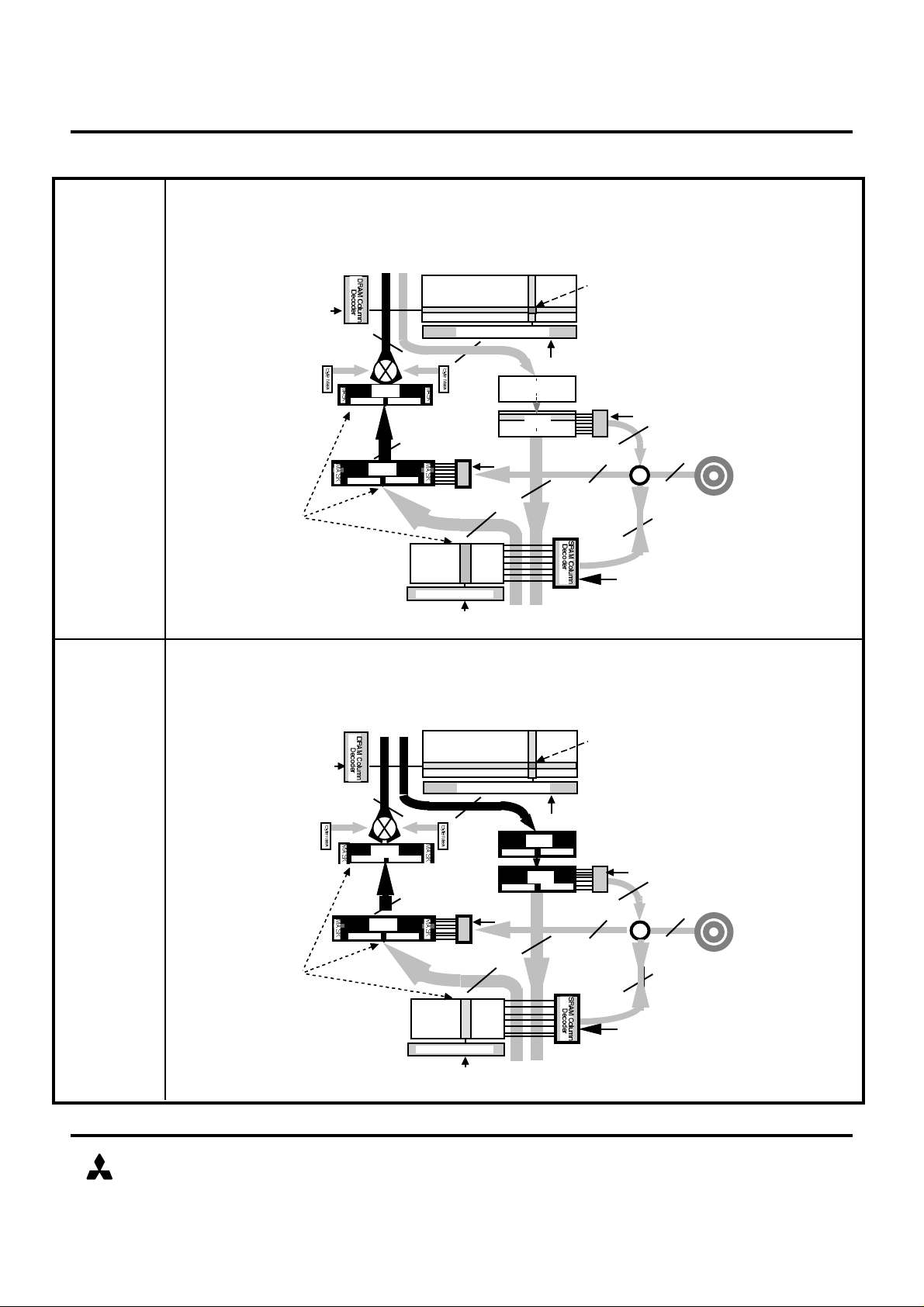
MODE DESCRIPTIONS (1)
DRAM
1MX16
16bits
SRAM RowDecoder
8X16
16MCDRAM:16M(1M-WORD BY 16-BIT) CACHED DRAM WITH 16K (1024-WORD BY 16-BIT) SRAM
NOP
SRAM
Deselect SRAM
SRAM Read
No Operation. Outputs are high-impedance. All input buffers remain
If CMs#=Low at the rising edge of K, the SRAM enters SRAM Power Down at the next
All transfer functions and input/output operations to and from the SRAM and Buffer are
disabled. This cycle is useful for output impedance control (Hi-Z,Low-Z) without G#. Output
Data is read from the SRAM to the I/O pins. Addresses As0-As9 are used to select the data
to be read. As3-As9 decode the SRAM Row (=Block), and As0-As2 decode (1 of 8) the 16bit word. DQCu and DQCl control the impedence (High-Z/Low-Z) of the upper and lower
bytes, respectively.
Data is written from the I/O pins to the SRAM. Addresses As0-As9 are used to select the
location to be written. As3-As9 decode the SRAM Row (=Block), and As0-As2 decode
(1of8) the 16-bit word to be written. DQCUu and DQCl control Upper and Lower byte
Ad3-7
1of32
SRAM Write
Lower Byte
Upper Byte
Upper ByteLower Byte
DQ8-15DQ0-7
SRAM
1KX16
As3-9
As0-2
1of8
Lower Byte
Lower Byte
Upper Byte
Upper Byte
Ad0-9
As0-2
DQs
X
As0-2
(REV 1.0) Jul. 1998MITSUBISHI ELECTRIC
8
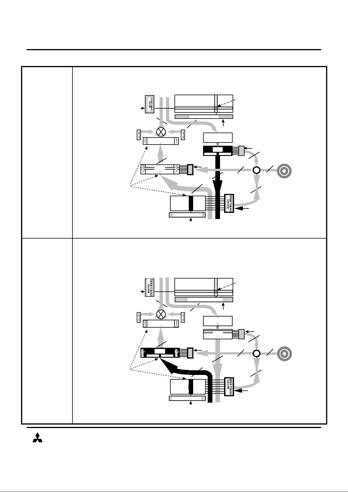
M5M4V16169DTP/RT-7,-8,-10,-15
MITSUBISHI LSIs
Transfer
SRAM row to which the 8X16 bit block is to be written. Addresses As0-As2 must be set low.
decode
the SRAM Row (=8X16 bit block) to be transferred. Addresses As0-As2 must be set low.
The Buffer Write Transfer cycle "clears" all transfer mask bits in the WB1 Mask (allowing all
data to be transferred in a successive DRAM Write Transfer cycle).
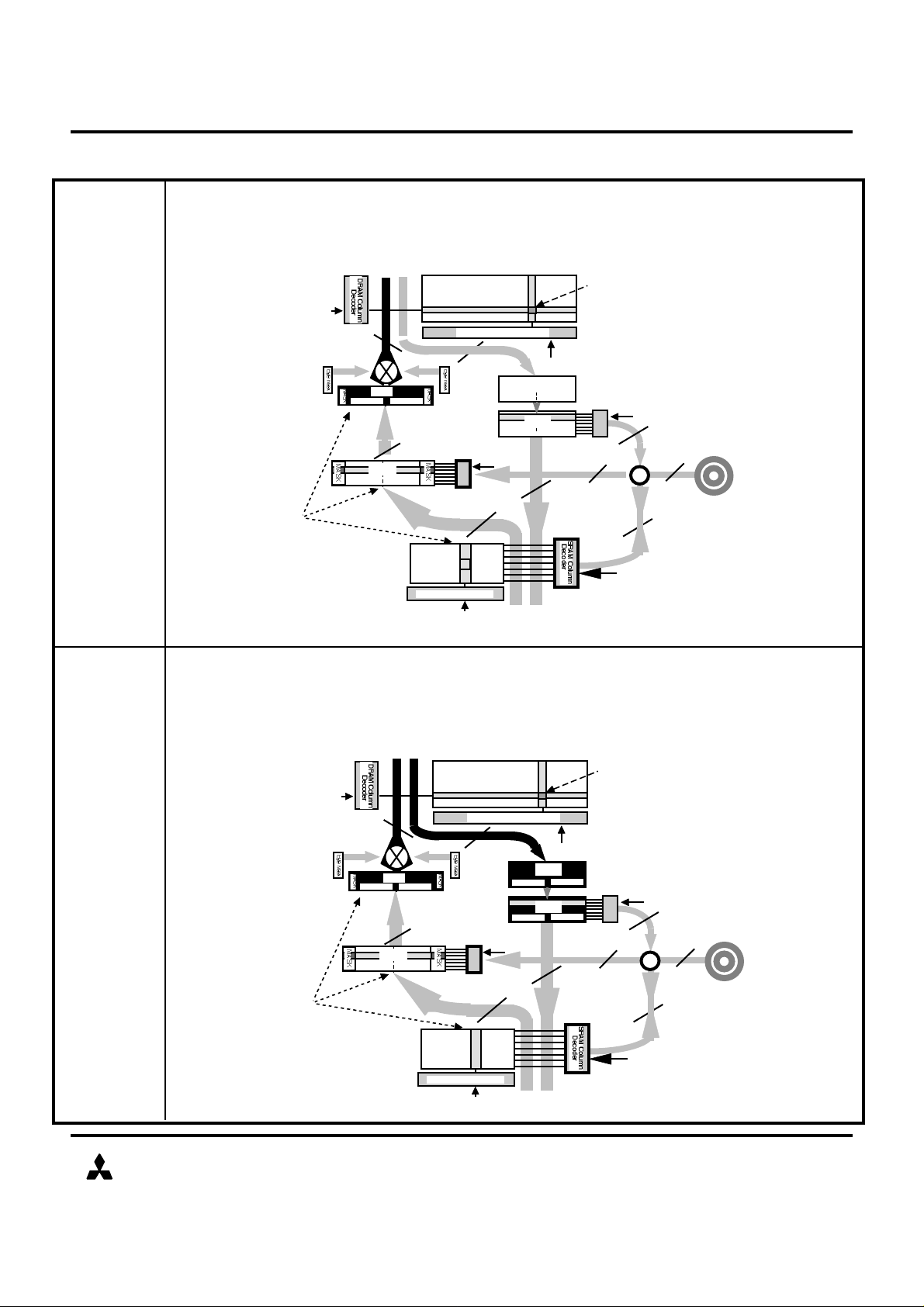
MODE DESCRIPTIONS (2)
8X16
8X16
8X16
8X16
8X16
16bits
16bits
16bits
1of128Decode
SRAM RowDecoder
DRAM
1M X 16
1of4096Decode
Decode
Decode
1of8Decode
8X16Block
8X16Block
WB1
WB2
DRAM RowDecoder
16bits
1of8Decode
RB2
RB1
8X16
8X16
8X16
8X16
8X16
16bits
16bits
16bits
1of128Decode
SRAM RowDecoder
DRAM
1M X 16
1of4096Decode
Decode
Decode
1of8Decode
8X16Block
8X16Block
WB1
WB2
DRAM RowDecoder
16bits
1of8Decode
RB2
RB1
Ad0-11
16MCDRAM:16M(1M-WORD BY 16-BIT) CACHED DRAM WITH 16K (1024-WORD BY 16-BIT) SRAM
Data is transferred from the Read Buffer (RB2) to the SRAM. Addresses As3-9 select the
Ad3-7
1of32
Ad0-11
Upper Byte
As0-2
1of8
Lower Byte
As0-2
Upper ByteLower Byte
X
Buffer Read
Lower Byte
Upper ByteLower Byte
Upper Byte
DQ8-15DQ0-7
DQs
Buffer Write
Transfer
SRAM
1KX16
As3-9
As0-2
Data is transferred from the SRAM to the Write-Buffer1 (WB1). Addresses As3-As9
Ad3-7
1of32
Upper Byte
As0-2
1of8
Lower Byte
Lower Byte
As0-2
Upper Byte
DQs
X
Lower Byte
Upper ByteLower Byte
Upper Byte
DQ8-15DQ0-7
SRAM
1KX16
As3-9
(REV 1.0) Jul. 1998MITSUBISHI ELECTRIC
As0-2
9
M5M4V16169DTP/RT-7,-8,-10,-15
MITSUBISHI LSIs
SRAM Read
read.
MODE DESCRIPTIONS (3)
8X16
8X16
8X16
8X16
8X16
16bits
16bits
16bits
1of128Decode
SRAM RowDecoder
DRAM
1M X 16
1of4096Decode
Decode
1of8Decode
1of8Decode
8X16Block
8X16Block
WB1
WB2
DRAM RowDecoder
16bits
1of8Decode
8X16
8X16
8X16
8X16
8X16
16bits
16bits
16bits
1of128Decode
SRAM RowDecoder
DRAM
1M X 16
1of4096Decode
Decode
Decode
1of8Decode
8X16Block
8X16Block
DRAM RowDecoder
16bits
1of8Decode
RB2
RB1
RB1
RB2
WB2
WB1
16MCDRAM:16M(1M-WORD BY 16-BIT) CACHED DRAM WITH 16K (1024-WORD BY 16-BIT) SRAM
Data is transferred from the Read Buffer (RB2) to the SRAM, and simultaneously, data (16
bit word) is read from the RB2 to the I/O pins. Addresses As3-9 select the SRAM Row to
which the 8X16 bit block is to be written. Addresses As0-As2 decode the 16-bit word to be
Ad3-7
1of32
Ad0-11
Buffer Read
Transfer &
Buffer Write
Transfer &
SRAM Write
Upper Byte
Lower Byte
Upper ByteLower Byte
Upper Byte
DQ8-15DQ0-7
Lower Byte
Upper ByteLower Byte
As0-2
As0-2
DQs
X
SRAM
1KX16
As3-9
As0-2
Data is first written from the I/O pins to SRAM as decoded by As0-As9. Then, the SRAM
Row (=Block) decoded by As3-As9 is transferred to the Write-Buffer1 (WB1). The Buffer
Write Transfer cycle "clears" all transfer mask bits in the WB1 Mask (allowing all data to be
transferred in a successive DRAM Write Transfer cycle). DQCu and DQCl control Upper
and Lower byte writes respectively, however all transfer mask bits in the WB1 are cleared.
Ad3-7
1of32
Ad0-11
Upper Byte
Lower Byte
Upper Byte
DQ8-15DQ0-7
Lower Byte
As0-2
Upper ByteLower Byte
SRAM
1KX16
As3-9
As0-2
1of8
Lower Byte
Upper Byte
DQs
X
As0-2
(REV 1.0) Jul. 1998MITSUBISHI ELECTRIC
10
M5M4V16169DTP/RT-7,-8,-10,-15
MITSUBISHI LSIs
bits), respectively.
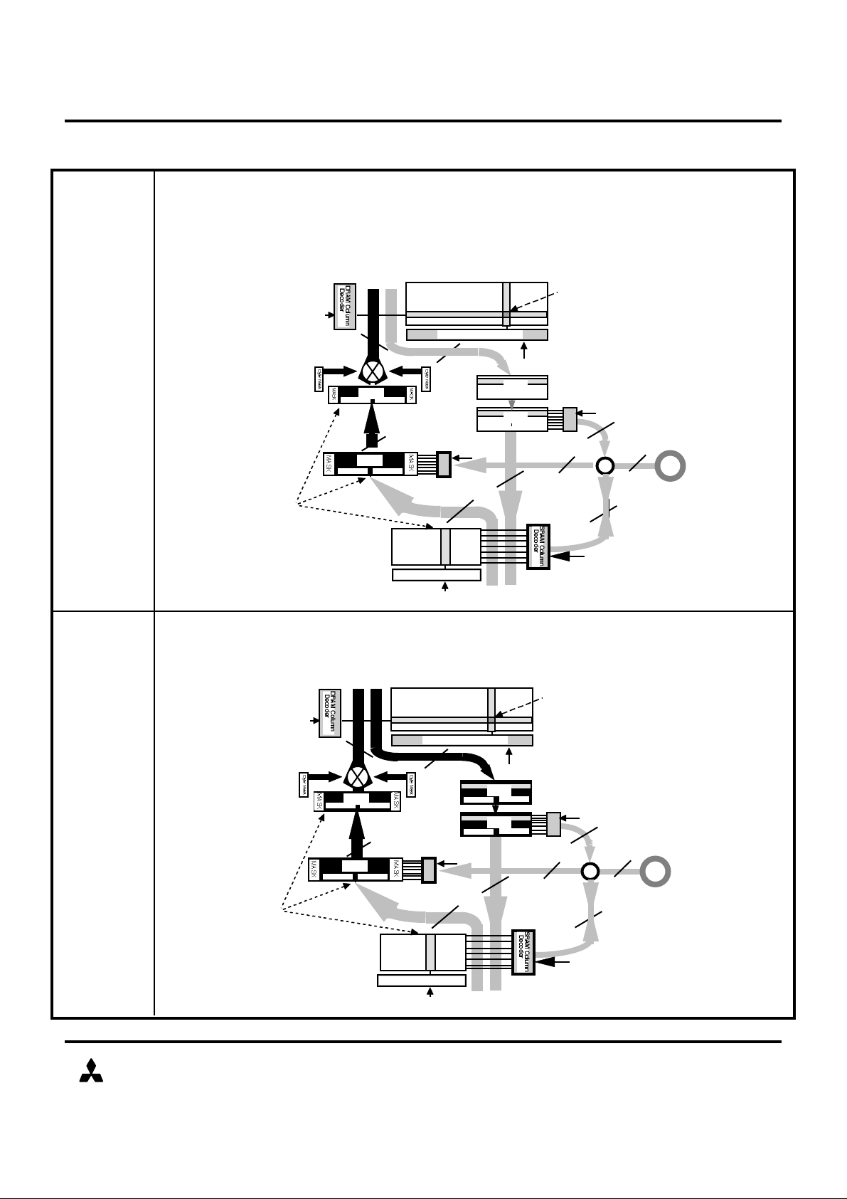
MODE DESCRIPTIONS (4)
8X16
8X16
8X16
8X16
8X16
16bits
16bits
16bits
1of128Decode
SRAM RowDecoder
DRAM
1M X 16
1of4096Decode
Decode
Decode
1of8Decode
8X16Block
8X16Block
WB1
DRAM RowDecoder
16bits
1of8Decode
RB2
8X16
8X16
8X16
8X16
8X16
16bits
16bits
16bits
1of128Decode
SRAM RowDecoder
DRAM
1M X 16
1of4096Decode
Decode
Decode
1of8Decode
8X16Block
8X16Block
WB1
WB2
DRAM RowDecoder
16bits
1of8Decode
RB2
RB1
WB2
RB1
16MCDRAM:16M(1M-WORD BY 16-BIT) CACHED DRAM WITH 16K (1024-WORD BY 16-BIT) SRAM
Data is read from the Read Buffer (RB2) to the I/O pins. Addresses As0-As2 are used to
select (1 of 8) the 16-bit word to be read. Addresses As3-As9 must be set low for this
operation.
Ad3-7
1of32
Ad0-11
Upper Byte
Buffer Read
Lower Byte
Upper ByteLower Byte
Upper Byte
As0-2
1of8
Lower Byte
Lower Byte
Upper Byte
DQ8-15DQ0-7
As0-2
DQs
X
Buffer Write
SRAM
1KX16
As3-9
As0-2
Data is written from the I/O pins to the Write-Buffer1. Addresses As0-A2 are used to select
(1of8) the 16-bit word to be written. Addresses As3-As9 must be set low for this operation.
The transfer mask bits associated with the Upper and Lower bytes are cleared in the WB1
Mask. DQCu and DQCl control Upper and Lower byte writes (and associated tranfer mask
Ad3-7
1of32
Ad0-11
Upper Byte
Lower Byte
Upper ByteLower Byte
Upper Byte
As0-2
1of8
Lower Byte
Lower Byte
Upper Byte
DQ8-15DQ0-7
As0-2
DQs
X
SRAM
1KX16
As3-9
As0-2
(REV 1.0) Jul. 1998MITSUBISHI ELECTRIC
11
M5M4V16169DTP/RT-7,-8,-10,-15
16MCDRAM:16M(1M-WORD BY 16-BIT) CACHED DRAM WITH 16K (1024-WORD BY 16-BIT) SRAM
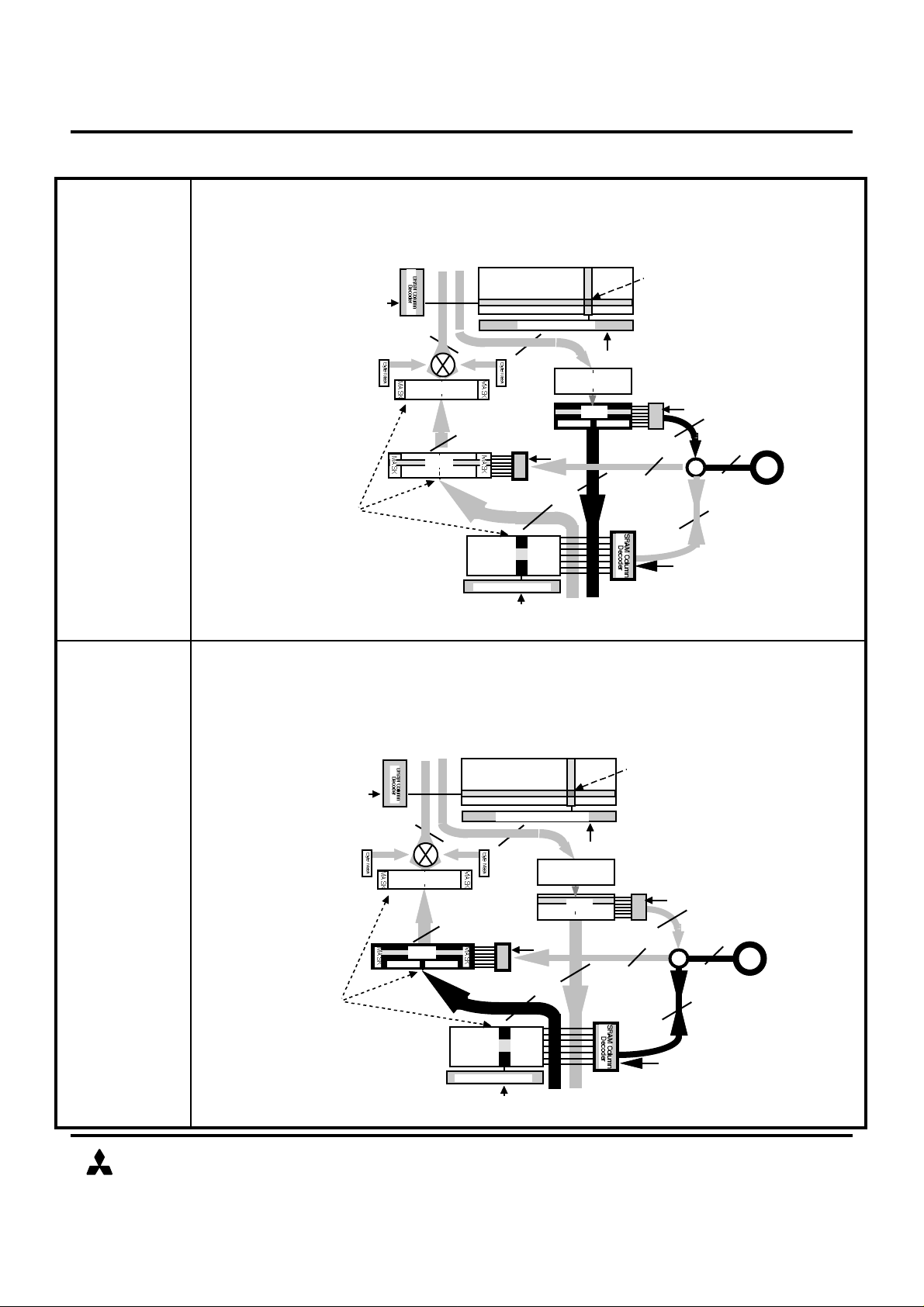
MODE DESCRIPTIONS (5)
Buffer2. Prior to the Latency timeout, old data will be present in the RB2. (Notes 1,2,4)
rising
edge of K. During this mode, the internal DRAM K clock becomes inactive. Also all input
buffers of DRAM clocks and DRAM addresses are inactive. Note that the latency of DRAM
Read Transfer cycle is not counted up in this cycle.
in
its present (precharge/activate) state.
8X16
8X16
8X16
8X16
8X16
16bits
16bits
16bits
1of128Decode
SRAM RowDecoder
DRAM
1M X 16
1of4096Decode
Decode
Decode
1of8Decode
8X16Block
8X16Block
WB1
DRAM RowDecoder
16bits
1of8Decode
RB2
RB1XWB2
DRAM
Power-Down
MITSUBISHI LSIs
If CMd#=Low at the rising edge of K, the DRAM enters DRAM Power Down at the next
DRAM NOP
DRAM Read
Transfer
The DNOP cycle is used when no other DRAM operations are desired, holding the DRAM
A Block (8x16) is transferred from the DRAM to the Read Buffer1 and 2 (RB1,RB2) as specified
by Addresses Ad3-Ad7. Addresses Ad8-Ad11 and Ad0-Ad2 must be set to Low. After the
Latency Period (specified in the Access Latency Table) new data will be present in the Read
Ad3-7
1of32
Ad0-11
Upper Byte
Lower Byte
Upper ByteLower Byte
Upper Byte
DQ8-15DQ0-7
SRAM
1KX16
As0-2
1of8
Lower Byte
Lower Byte
Upper Byte
As0-2
DQs
As0-2
As3-9
MITSUBISHI ELECTRIC
(REV 1.0) Jul. 1998
12
M5M4V16169DTP/RT-7,-8,-10,-15
16MCDRAM:16M(1M-WORD BY 16-BIT) CACHED DRAM WITH 16K (1024-WORD BY 16-BIT) SRAM
Transfer1
& Read
which
the data is written in DRAM is simultaneously transferred to the Read Buffer.(Notes 2,3,4)
8X16
8X16
8X16
8X16
8X16
16bits
16bits
16bits
1of128Decode
SRAM RowDecoder
DRAM
1M X 16
1of4096Decode
Decode
Decode
1of8Decode
8X16Block
8X16Block
WB1
WB2
DRAM RowDecoder
16bits
1of8Decode
RB2
RB1
8X16
8X16
8X16
8X16
8X16
16bits
16bits
16bits
1of128Decode
SRAM RowDecoder
DRAM
1M X 16
1of4096Decode
Decode
Decode
1of8Decode
8X16Block
8X16Block
WB1
DRAM RowDecoder
16bits
1of8Decode
RB2
RB1
Ad0-11
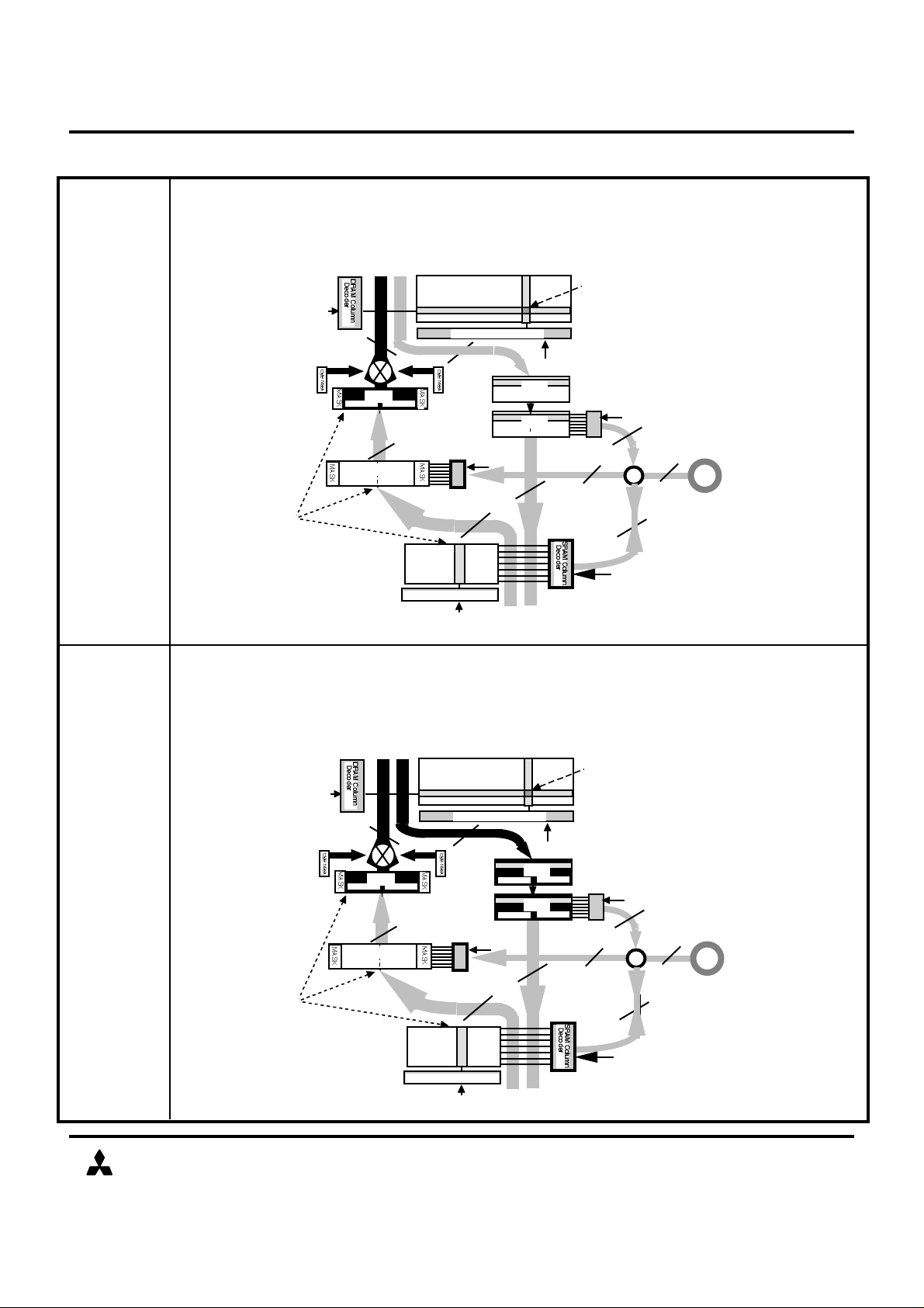
MODE DESCRIPTIONS (6)
WB2
DRAM Write
MITSUBISHI LSIs
Data (8X16 Block) is transferred from WB1 through WB2 to the DRAM block specified by
Addresses Ad3-Ad7. Addresses Ad8-Ad11 must be set to Low. The Mask present in WB1 is
also transferred to WB2 and controls the data written to the DRAM. After data has been
transferred from WB1 to WB2 in the present cycle, the entire WB1 Mask is Set. (Notes 3,4)
Ad3-7
1of32
Upper Byte
As0-2
1of8
Lower Byte
Lower Byte
As0-2
Upper Byte
DQs
Upper ByteLower Byte
DQ8-15DQ0-7
DRAM Write
Transfer1
Lower Byte
Upper Byte
X
SRAM
1KX16
As3-9
As0-2
Data (8X16 Block) is transferred from WB1 through WB2 to the DRAM block specified by
Addresses Ad3-Ad7. Addresses Ad8-A11 must be set to Low. The transfer mask present in
WB1 is also transferred to WB2 and controls the data written to the DRAM. The block to
Ad3-7
1of32
Ad0-11
Upper Byte
As0-2
1of8
Lower Byte
Lower Byte
Upper Byte
Upper ByteLower Byte
DQ8-15DQ0-7
As0-2
DQs
Upper Byte
Lower Byte
SRAM
1KX16
As3-9
MITSUBISHI ELECTRIC
X
As0-2
(REV 1.0) Jul. 1998
13
M5M4V16169DTP/RT-7,-8,-10,-15
MITSUBISHI LSIs
Transfer2
unchanged.
(Note 4)
the
Read Buffer1 and 2. (Notes 1,2,4)
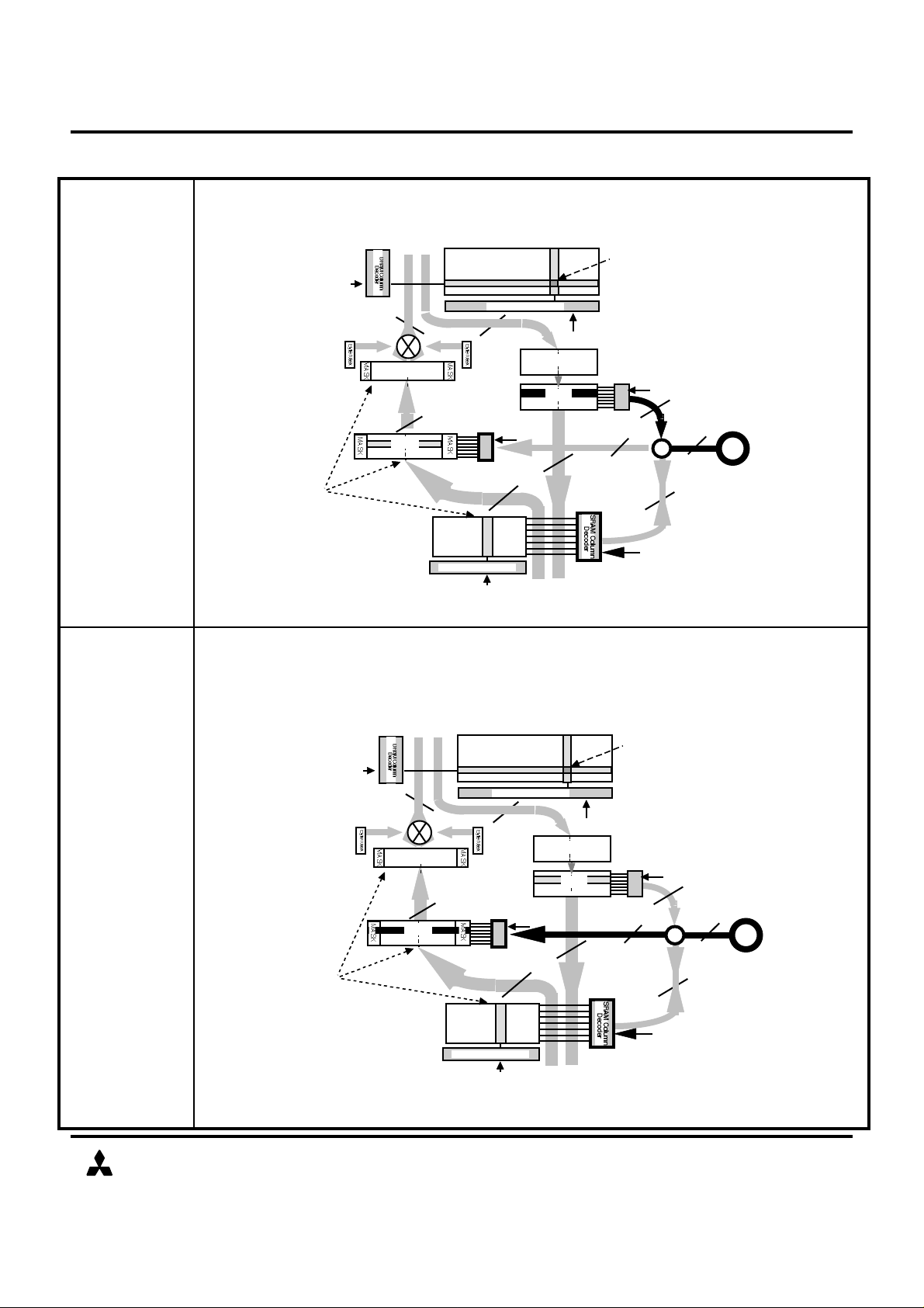
MODE DESCRIPTIONS (7)
8X16
8X16
8X16
8X16
8X16
16bits
16bits
1of128Decode
1of4096Decode
Decode
Decode
1of8Decode
8X16Block
8X16Block
WB1
DRAM RowDecoder
16bits
1of8Decode
RB2
RB1
Ad0-11
8X16
8X16
8X16
8X16
16bits
16bits
1of128Decode
1of4096Decode
Decode
Decode
1of8Decode
8X16Block
8X16Block
WB1
WB2
DRAM RowDecoder
16bits
1of8Decode
RB2
RB1
Ad0-11
WB2
SRAM RowDecoder
DRAM
1M X 16
16bits
SRAM
1KX16
DRAM
1MX16
8X16
16bits
SRAM RowDecoder
16MCDRAM:16M(1M-WORD BY 16-BIT) CACHED DRAM WITH 16K (1024-WORD BY 16-BIT) SRAM
Data (8X16 Block) is transferred from WB2 to the DRAM block specified by Addresses Ad3Ad7. Addresses Ad8-Ad11 must be set to Low. The WB2 Mask controls the data written to
the DRAM. With the DWT2 function, the WB2 data and WB2 transfer mask remain
Ad3-7
1of32
DRAM Write
Upper Byte
As0-2
1of8
Lower Byte
Lower Byte
As0-2
Upper Byte
DQs
X
Lower Byte
Upper ByteLower Byte
Upper Byte
DQ8-15DQ0-7
SRAM
1KX16
As3-9
As0-2
Data (8X16 Block) is transferred from WB2 to the DRAM block specified by Addresses Ad3Ad7. Addresses Ad8-Ad11 must be set to Low. The WB2 transfer mask controls the data
written to the DRAM. With the DWT2 function, the WB2 data and WB2 transfer mask remain
unchanged. The block to which the data is written in DRAM is simultaneously transferred to
Ad3-7
1of32
DRAM Write
Transfer2
& Read
Lower Byte
Upper ByteLower Byte
Upper Byte
DQ8-15DQ0-7
As3-9
MITSUBISHI ELECTRIC
As0-2
1of8
Lower Byte
Lower Byte
Upper Byte
Upper Byte
As0-2
DQs
X
As0-2
(REV 1.0) Jul. 1998
14
M5M4V16169DTP/RT-7,-8,-10,-15
16MCDRAM:16M(1M-WORD BY 16-BIT) CACHED DRAM WITH 16K (1024-WORD BY 16-BIT) SRAM
Transfer3
& Read
MODE DESCRIPTIONS (8)
8X16
8X16
8X16
8X16
8X16
16bits
16bits
16bits
1of128Decode
SRAM RowDecoder
DRAM
256KX16
1of4096Decode
Decode
Decode
1of8Decode
8X16Block
8X16Block
WB1
WB2
DRAM RowDecoder
16bits
1of8Decode
RB2
RB1
8X16
8X16
8X16
8X16
8X16
16bits
16bits
16bits
1of128Decode
SRAM RowDecoder
DRAM
256KX16
1of4096Decode
Decode
Decode
1of8Decode
8X16Block
8X16Block
WB1
WB2
DRAM RowDecoder
16bits
1of8Decode
RB2
RB1
DRAM Write
MITSUBISHI LSIs
Data (8X16 Block) is transferred from WB1 through WB2 to the DRAM block specified by
Addresses Ad3-Ad7. Addresses Ad8-Ad9 must be set to Low. The Mask present in Byte
MaskRegister controls the data written to the DRAM. The Byte Mask Register is set at Load Byte
Mask cycle,where corresponding byte masks are set depending on DQ data in the cycle. (Note
4,5) The data of WB1 and the mask data of WBM1 are tranferred to WB2 and WBM2, however
WBM1/2 is not used in this cycle.
Ad3-7
1of32
Ad0-11
Upper Byte
As0-2
1of8
Lower Byte
Lower Byte
As0-2
Upper Byte
DQs
X
Lower Byte
Upper ByteLower Byte
Upper Byte
DQ8-15DQ0-7
DRAM Write
Transfer3
SRAM
1KX16
As3-9
As0-2
Data (8X16 Block) is transferred from WB1 through WB2 to the DRAM block specified by
Addresses Ad3-Ad7. Addresses Ad8-Ad9 must be set to Low. The Mask present in Byte
MaskRegister controls the data written to the DRAM. The block to which the data is written in
DRAM is simultaneously transferred to the Read Buffer.(Notes 1,2,4,5)
Ad3-7
1of32
Ad0-11
Upper Byte
As0-2
1of8
Lower Byte
Lower Byte
As0-2
Upper Byte
DQs
X
As0-2
Lower Byte
Upper ByteLower Byte
Upper Byte
DQ8-15DQ0-7
SRAM
1KX16
As3-9
MITSUBISHI ELECTRIC
(REV 1.0) Jul. 1998
15
M5M4V16169DTP/RT-7,-8,-10,-15
16MCDRAM:16M(1M-WORD BY 16-BIT) CACHED DRAM WITH 16K (1024-WORD BY 16-BIT) SRAM
Transfer4
remain unchanged. (Note 4,5)
MODE DESCRIPTIONS (9)
8X16
8X16
8X16
8X16
8X16
16bits
16bits
16bits
1of128Decode
SRAM RowDecoder
DRAM
256KX16
1of4096Decode
Decode
Decode
1of8Decode
8X16Block
8X16Block
WB1
WB2
DRAM RowDecoder
16bits
1of8Decode
RB2
RB1
8X16
8X16
8X16
8X16
8X16
16bits
16bits
1of128Decode
SRAM RowDecoder
DRAM
256KX16
1of4096Decode
Decode
Decode
1of8Decode
8X16Block
8X16Block
WB2
DRAM RowDecoder
16bits
1of8Decode
RB2
RB1
WB1
16bits
DRAM Write
MITSUBISHI LSIs
Data (8X16 Block) is transferred from WB2 to the DRAM block specified by Addresses Ad3Ad7. Addresses Ad8-Ad9 must be set to Low. The Mask present in Byte MaskRegister
controls the data written to the DRAM. With the DWT4 function, the WB2 data and WB2 Mask
Ad3-7
1of32
Ad0-11
Upper Byte
As0-2
1of8
Lower Byte
Lower Byte
As0-2
Upper Byte
DQs
X
Lower Byte
Upper ByteLower Byte
Upper Byte
DQ8-15DQ0-7
DRAM Write
Transfer4
& Read
SRAM
1KX16
As3-9
As0-2
Data (8X16 Block) is transferred from WB2 to the DRAM block specified by Addresses Ad3Ad7. Addresses Ad8-Ad9 must be set to Low. The Mask present in Byte MaskRegister
controls the data written to the DRAM. With the DWT4R function, the WB2 data and WB2
transfer mask remain unchanged. The block to which the data is written in DRAM is
simultaneously transferred to the Read Buffer. (Notes 1,2,4,5)
Ad3-7
1of32
Ad0-11
Upper Byte
As0-2
1of8
Lower Byte
Lower Byte
As0-2
Upper Byte
DQs
X
Lower Byte
Upper ByteLower Byte
Upper Byte
DQ8-15DQ0-7
SRAM
1KX16
As3-9
MITSUBISHI ELECTRIC
As0-2
(REV 1.0) Jul. 1998
16
M5M4V16169DTP/RT-7,-8,-10,-15
MITSUBISHI LSIs
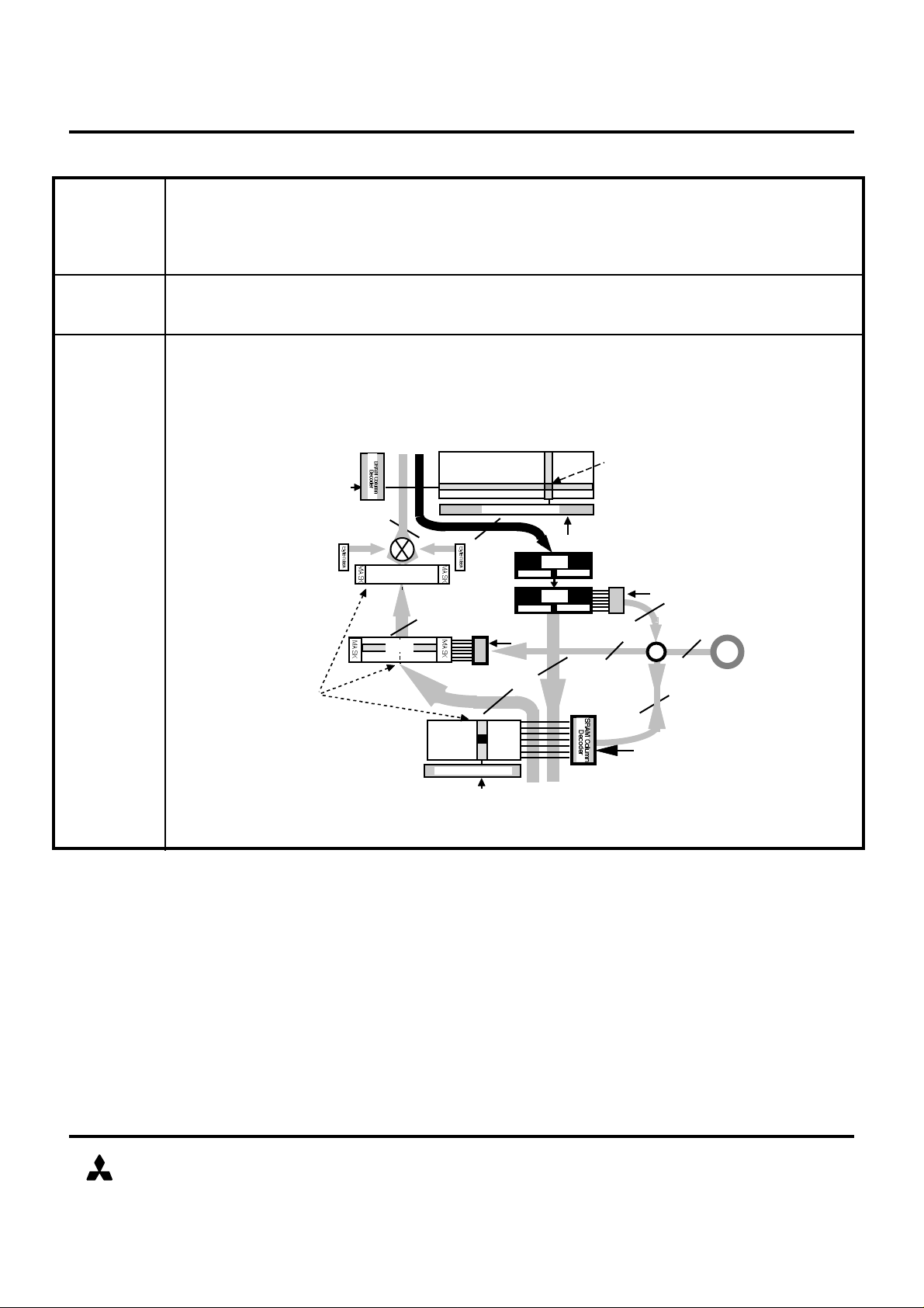
MODE DESCRIPTIONS (10)
Activate
Auto-Refresh
is
selected (Page Call) in preparation for a DRAM Read or Write Transfer cycle. A DRAM Precharge
cycle must separate all DRAM Activate cycles.
Register
Power-On sequence
16MCDRAM:16M(1M-WORD BY 16-BIT) CACHED DRAM WITH 16K (1024-WORD BY 16-BIT) SRAM
DRAM
DRAM
Precharge
DRAM
DRAM
Self Refresh
Set
Command
Addresses are latched from the Ad0-Ad11 inputs by the rising edge of K. Internally, a DRAM row
Internally, the active DRAM Row is deselected (completing the refresh process) and page-mode is
disabled. The DRAM is precharged prior to another DRAM Activate cycle.
Internally, a DRAM row is selected and refreshed (as addressed by an internal, self-incrementing
counter), followed by an internally generated Precharge cycle. The Auto refresh cycle can be
implemented only if the DRAM is in Precharge state (i.e., a Precharge or Auto-Refresh cycle
occurred more recently than an Acitvate cycle). DRAM Auto-Refresh is similar to a CAS-BeforeRAS (CBR) mode in standard DRAMs.
All clock buffers are suspended, and CMd# asynchronously controls Self Refresh (CMd# rising
edge initiates exit from Self Refresh). During Self Refresh, device enters a low power mode, with
2048 automatic refresh cycles.
When SCR is initiated,the addresses present on the Ad0-Ad11 DRAM Address pins determine the
DRAM Read Transfer Latency, the Output Mode (transparent / latched / registered), and WB1
transfer mask mode (set-all/ no change). No DRAM operation is executed in this cycle. Refer to
the SCR Truth Table for legal Address values.
During SCR cycle and the following 3 clock cycles(totally 4 clock cycles), only NOP,DNOP orDPD
are allowed in DRAM portion and only NOP,DES or SPD are done in SRAM portion. The set
commands are valid at least after the above 4 clocks later and the previous function is not
guaranteed to work if it has not been completed.(i.e. DRT ,DWT1&R,DWT2&R and SR,BR and
BRTR with registered output mode.)
Notes:
1) This function is performed in a Latency period specified in the Access Latency Table.
2) After the Latency Period (specified in the Access Latency Table) new data will be present
in the Read Buffer2. Prior to the Latency timeout, old data will be present in the RB2.
3) After data has been transferred from WB1, the entire WB1 Mask is Set.
4) Valid Ad0-Ad2 addresses are shown in the FUNCTION TRUTH TABLE.
Before starting normal operation, the following power on sequence is necessary.
1) Apply power and maintain stable power (pause) for 500us.
2) Perform a precharge (PCG) operation.
3) After tRP, perform 8 auto refresh commands (ARF) with adequate interval (tRC).
4) Issue set command register (SCR) to initilize the mode register.
After this sequence, the RAM is in idle state and ready for normal operation.
Note that DNOP / DPD and DES / SPD or NOP command will be the stand-by command
for the above power sequence.
Vcc must be powered-on at the same time or before VccQ is on.
And Vcc must be powered-off at the same time or after VccQ is off.
MITSUBISHI ELECTRIC
(REV 1.0) Jul. 1998
17
M5M4V16169DTP/RT-7,-8,-10,-15
16MCDRAM:16M(1M-WORD BY 16-BIT) CACHED DRAM WITH 16K (1024-WORD BY 16-BIT) SRAM
tKLA
tKLQX
tKLQZ
tGHQ
tKHA
tGLQ
tGLA
tKLA
tKHA
tKHA
tKHQX
tKHQZ
tGLQQtGHQ
tGLA
tKHA
tKHQX
tKHQZ
tGLQQtGHQ
tKHAR
tKHQZ
tGLA
tK
tKHAR
tK
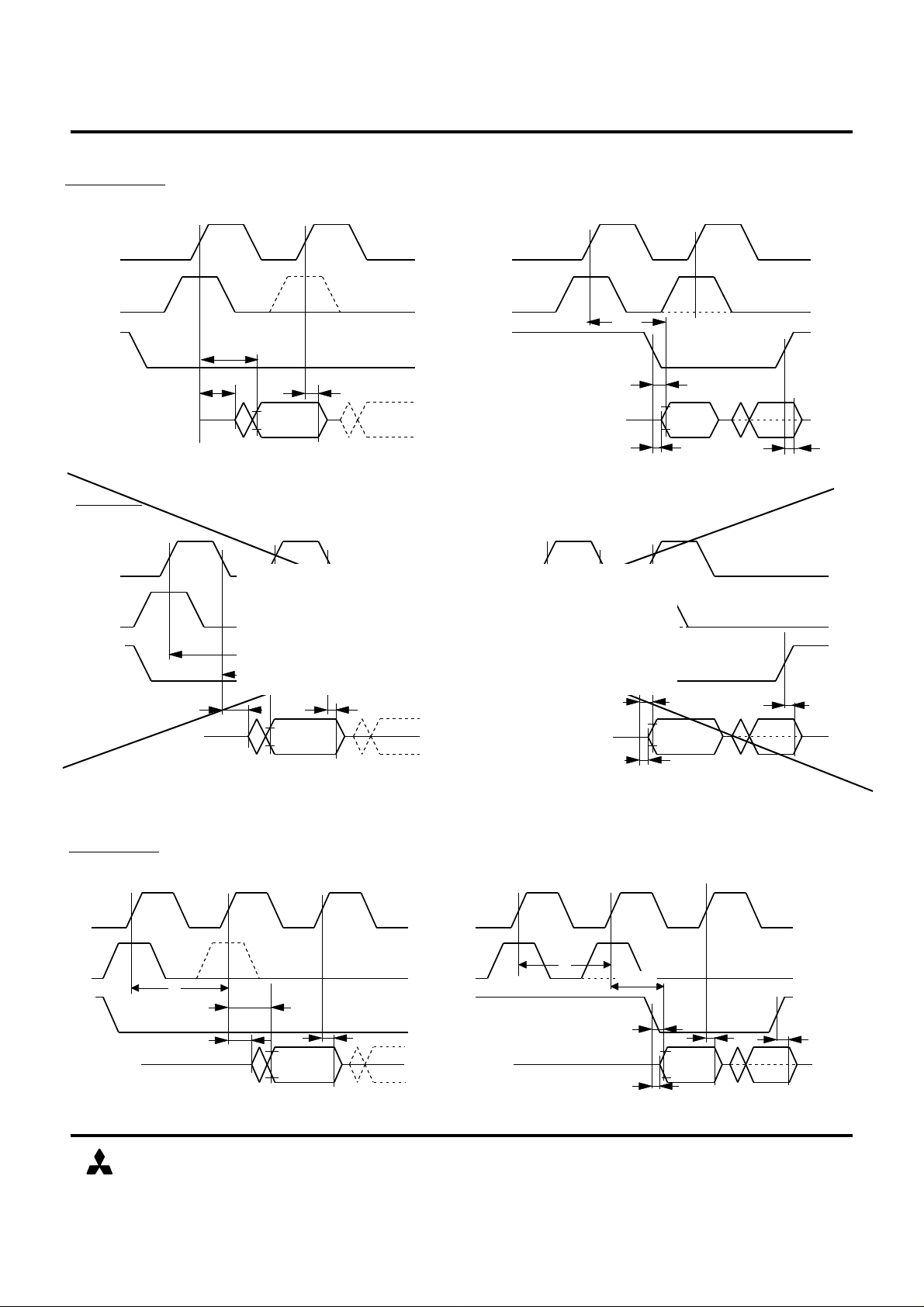
Output Operations
Transparent
MITSUBISHI LSIs
Output appears from the rising edge of K clock.
K
DQC
G#
DQ0-15
Latched
DES
K
DQC
DES
SR
SR
SR
DES
K
DQC
G#
Q
Output appears from the falling edge of K clock.
SR
DQ0-15
DES
SR
K
This outputmode
DQC
SR SR
SR
G#
DQ0-15
Registered
DES
K
DQC
G#
DQ0-15
SR
was deleted.
Q
Output appears from the rising edge of K clock.
SR
SR
G#
DQ0-15
DES
SR
K
DQC
G#
Q
DQ0-15
SR
Q
SR
MITSUBISHI ELECTRIC
(REV 1.0) Jul. 1998
18
M5M4V16169DTP/RT-7,-8,-10,-15
MITSUBISHI LSIs
As0-9
tH
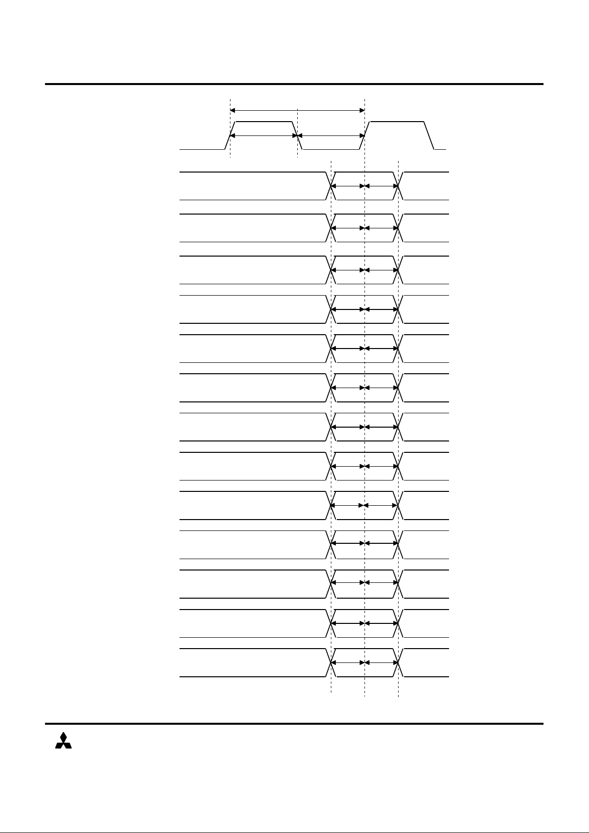
16MCDRAM:16M(1M-WORD BY 16-BIT) CACHED DRAM WITH 16K (1024-WORD BY 16-BIT) SRAM
tK
tKH tKL
K,K#
tS
CMd#
CS#
RAS#
CAS#
DTD#
CMs#
CC0#
CC1#
tCMDS tCMDH
tCSS tCSH
tRS tRH
tCS tCH
tDTS tDTH
tCMSS tCMSH
tC0S tC0H
tC1S tC1H
WE#
DQC(u / l)
ADF#
Ad0-11
DQ0-15
(Input)
MITSUBISHI ELECTRIC
tWS tWH
tDQCS tDQCH
tSADF tHADF
tAS tAH
tDS tDH
(REV 1.0) Jul. 1998
19
M5M4V16169DTP/RT-7,-8,-10,-15
16MCDRAM:16M(1M-WORD BY 16-BIT) CACHED DRAM WITH 16K (1024-WORD BY 16-BIT) SRAM
(16 byte)
23456
7
Load Byte Mask
Byte mask allocation during DWT3 and DWT4
Byte Mask Register
MITSUBISHI LSIs
DQ0
Lower
Upper
Block
address
0
Column Block
Lower DQs
DQ1
DQ2
1
DQ3
DQ4
DQ5
DQ6
DQ7
DQ8
Upper DQs
DQ10
DQ9
DQ11
DQ12
DQ13
DQ14
DQ15
0 : mask, no write
1 : unmask, write enable
MITSUBISHI ELECTRIC
(REV 1.0) Jul. 1998
20
 Loading...