

MITSUBISHI SEMICONDUCTOR <TRANSISTOR ARRAY>
M54585KP
8-UNIT 500mA DARLINGTON TRANSISTOR-ARRAY WITH CLAMP DIODE
DESCRIPTION
M54585KP is eight-circuit Darlington transistor arrays with
clamping diodes. The circuits are made of NPN transistors.
Both the semiconductor integrated circuits perform high-current driving with extremely low input-current supply.
FEATURES
●
High breakdown voltage (BVCEO ≥ 50V)
●
High-current driving (IC(max) = 500mA)
●
With clamping diodes
●
Driving available with TTL output or with PMOS IC output
●
With shrink small outline package
APPLICATION
Drives of relays and printers, digit drives of indication elements such as LEDs and lamps, and MOS-bipolar logic IC
interfaces
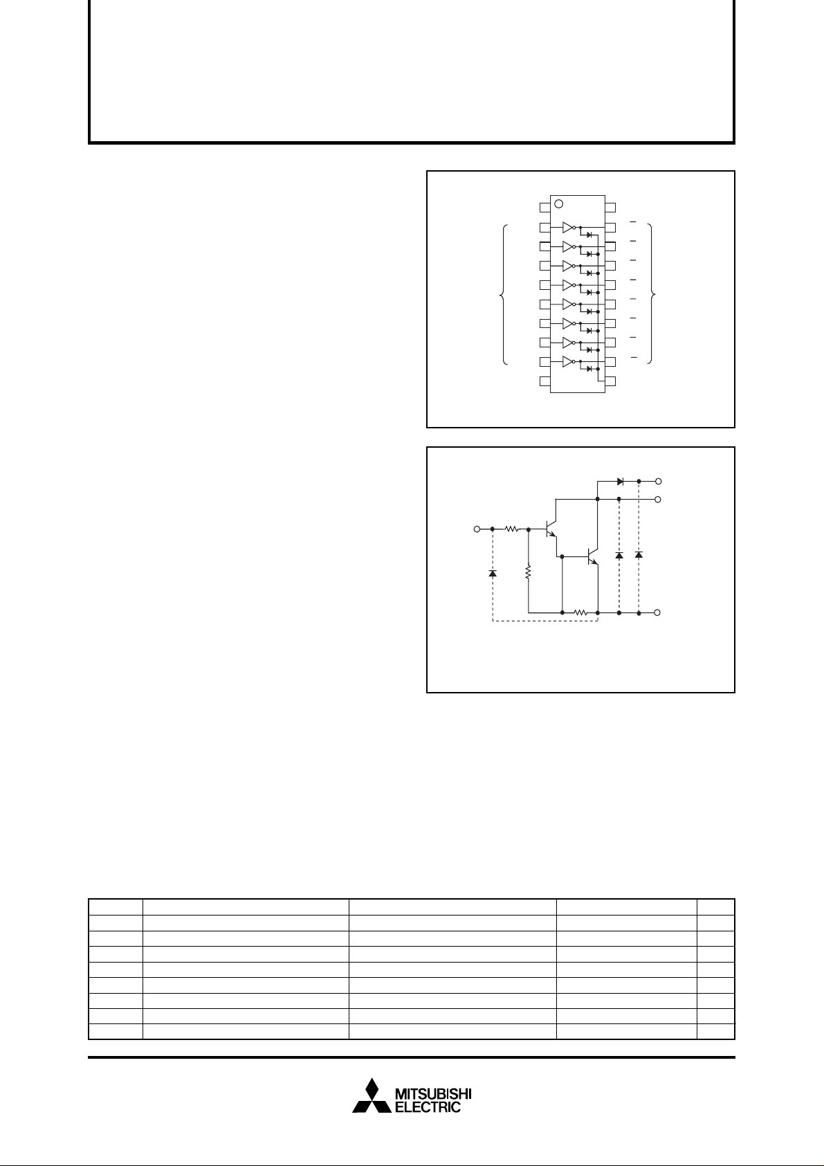
PIN CONFIGURATION
1
NC
2
IN1→
→
IN2
3
IN3→
4
5
→
INPUT
IN4
IN5→
IN6
IN7→
IN8
6
→
7
8
→
9
10
Package type 20P2E-A
CIRCUIT DIAGRAM
INPUT
2.7k
7.2k
20
NC
→
19
O1
→
18
O2
→
17
O3
→
16
O4
→
15
O5
→
14
O6
→
13
O7
→
12
O8
11
→COM COMMONGND
OUTPUT
NC : No connection
COM
OUTPUT
FUNCTION
The M54585KP has eight circuits, which are NPN Darlington
transistors. Input transistors have resistance of 2.7kΩ be-
The diode, indicated with the dotted line, is parasitic, and cannot
be used.
tween the base and input pin. A spike-killer clamping diode
is provided between each output pin and GND. Output transistor emitters are all connected to the GND pin.
Collector current is 500mA maximum. The maximum collector-emitter voltage is 50V.
ABSOLUTE MAXIMUM RATINGS (Unless otherwise noted, Ta = –20 ~ +75°C)
VCEO
IC
VI
IF
VR
Pd
Topr
Tstg
Collector-emitter voltage
Collector current
Input voltage
Clamping diode forward current
Clamping diode reverse voltage
Power dissipation
Operating temperature
Storage temperature
Output, H
Current per circuit output, L
Ta = 25°C, when mounted on board
3k
The eight circuits share the COM and GND.
GND
RatingsSymbol Parameter Conditions Unit
–0.5 ~ +50
500
–0.5 ~ +30
500
50
0.68
–20 ~ +75
–55 ~ +125
Unit : Ω
V
mA
V
mA
V
W
°C
°C
Jan. 2000
MITSUBISHI SEMICONDUCTOR <TRANSISTOR ARRAY>
M54585KP
8-UNIT 500mA DARLINGTON TRANSISTOR-ARRAY WITH CLAMP DIODE
RECOMMENDED OPERATING CONDITIONS (Unless otherwise noted, Ta = –20 ~ +75°C)
3.4
Limits
—
0
0
—
200
50
V
mA
0
—
—
—
—
0
70
30
30
0.6
V
V
V
Limits
+
1.3
1.0
8.7
1.5
max
—
2.4
1.6
1.8
18
2.4
100
—
V
mA
V
µA
—
min typ
50
—
—
—
—
—
—
1000
—
0.95
—
2500
Symbol Unit
V
O Output voltage
Collector current
(Current per 1 cir-
IC
cuit when 8 circuits
are coming on simultaneously)
VIH
VIL
“H” input voltage
“L” input voltage
Parameter
Duty Cycle ≤ 10%
Duty Cycle ≤ 50%
Ic ≤ 400mA
Ic ≤ 200mA
min typ max
3.85
ELECTRICAL CHARACTERISTICS (Unless otherwise noted, Ta = –20 ~ +75°C)
Symbol UnitParameter Test conditions
V
(BR) CEO
VCE(sat)
II
VF
IR
hFE
+ : The typical values are those measured under ambient temperature (Ta) of 25°C. There is no guarantee that these values are obtained under any
conditions.
Collector-emitter breakdown voltage
Collector-emitter saturation voltage
Input current
Clamping diode forward voltage
Clamping diode reverse current
DC amplification factor
CEO = 100µA
I
I = 3.85V, IC = 400mA
V
I = 3.4V, IC = 200mA
V
I = 3.85V
I
I = 25V
V
F = 400mA
I
R = 50V
V
CE = 4V, IC = 350mA, Ta = 25°C
V
V
SWITCHING CHARACTERISTICS (Unless otherwise noted, Ta = 25°C)
Symbol UnitParameter Test conditions
ton
toff
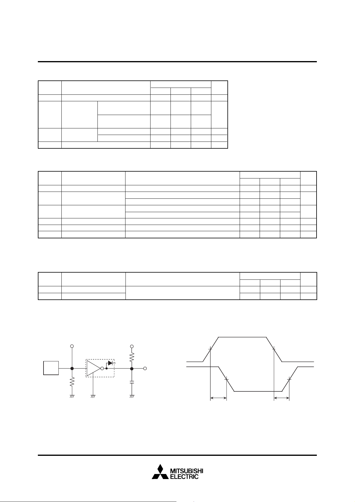
NOTE 1 TEST CIRCUIT
Turn-on time
Turn-off time
INPUT
Measured device
PG
50Ω
(1)Pulse generator (PG) characteristics : PRR = 1kHz,
tw = 10µs, tr = 6ns, tf = 6ns, Zo = 50Ω,
V
I
= 3.85V
(2)Input-output conditions : R
(3)Electrostatic capacity C
connections and input capacitance at probes
L
L
includes floating capacitance at
CL = 15pF (note 1)
OPEN
= 25Ω, Vo = 10V
TIMING DIAGRAM
Vo
R
L
OUTPUT
C
L
INPUT
OUTPUT
min typ max
50%
50%
ton toff
Limits
—
—
12
240
—
—
50%
ns
ns
50%
Jan. 2000

TYPICAL CHARACTERISTICS
MITSUBISHI SEMICONDUCTOR <TRANSISTOR ARRAY>
M54585KP
8-UNIT 500mA DARLINGTON TRANSISTOR-ARRAY WITH CLAMP DIODE
Thermal Derating Factor Characteristics
1.0
0.8
0.68
0.6
0.4
0.2
Power dissipation Pd (W)
0
0 25 50 75 100
Ambient temperature Ta (°C)
Duty Cycle-Collector Characteristics
500
400
300
200
•
Collector current Ic (mA)
The collector current values
100
represent the current per circuit.
•
Repeated frequency ≥ 10Hz
•
The value in the circle represents the
value of the simultaneously-operated circuit.
0
0
20 40 60 80
0.408
•Ta = 25°C
100
Output Saturation Voltage
Collector Current Characteristics
500
VI = 3.4V
400
300
200
Collector current Ic (mA)
100
Ta = 75°C
0
0 0.5 1.0 1.5 2.0
Output saturation voltage V
Ta = 25°C
Ta = –20°C
CE(sat)
(V)
Duty Cycle-Collector Characteristics
500
400
1
2
3
4
5
6
7
8
300
200
100
Collector current Ic (mA)
•
The collector current
values represent the current
per circuit.
•Repeated frequency ≥ 10Hz
•
The value in the circle represents the value of the simultaneously-operated circuit.
•
Ta = 75°C
0
20 40 60 80
0
100
1
2
3
4
5
6
7
8
Duty cycle (%)
DC Amplification Factor
Collector Current Characteristics
4
10
VCE = 4V
7
5
FE
3
2
3
10
7
5
3
DC amplification factor h
2
2
10
1
23 57 23 57
10
Collector current Ic (mA)
Ta = 75°C
2
10
Ta = –20°C
Ta = 25°C
10
Duty cycle (%)
Grounded Emitter Transfer Characteristics
500
VCE = 4V
400
300
200
Ta = 75°C
100
0
0
0
Ta = 25°C
Ta = –20°C
1234
Input voltage V
I
(V)
Jan. 2000
Collector current Ic (mA)
3

MITSUBISHI SEMICONDUCTOR <TRANSISTOR ARRAY>
M54585KP
8-UNIT 500mA DARLINGTON TRANSISTOR-ARRAY WITH CLAMP DIODE
Input Characteristics
10
Ta = –20°C
(mA)
I
8
6
4
Input current I
2
0
0 5 10 15 25
Input voltage V
Ta = 25°C
Ta = 75°C
I
(V)
20
Clamping Diode Characteristics
500
400
(mA)
F
300
200
100
Forward bias current I
Ta = 75°C
0
0 0.5 1.0 1.5 2.0
Forward bias voltage V
Ta = 25°C
Ta = –20°C
F
(V)
Jan. 2000
 Loading...