

MITSUBISHI SEMICONDUCTOR <TRANSISTOR ARRAY>
M54583P/FP
8-UNIT 400mA DARLINGTON TRANSISTOR ARRAY
DESCRIPTION
M54583P and M54583FP are eight-circuit collector-currentsynchronized Darlington transistor arrays. The circuits are
made of PNP and NPN transistors. Both the semiconductor
integrated circuits perform high-current driving with extremely low input-current supply.
FEATURES
●
High breakdown voltage (BVCEO ≥ 50V)
●
High-current driving (Ic(max) = 400mA)
●
Active L-level input
●
With input clamping diodes
APPLICATION
Interfaces between microcomputers and high-voltage, highcurrent drive systems, drives of relays and printers, and
MOS-bipolar logic IC interfaces
FUNCTION
The M54583 is produced by adding PNP transistors to
M54523 inputs. Eight circuits having active L-level inputs are
provided.
Resistance of 7kΩ and diode are provided in series between
each input and PNP transistor base. The input diode is intended to prevent the flow of current from the input to the
V
CC. Without this diode, the current flow from “H” input to the
V
CC and the “L” input circuits is activated, in such case where
one of the inputs of the 8 circuits is “H” and the others are “L”
to save power consumption. The diode is inserted to prevent
such misoperation.
This device is most suitable for a driver using NMOS IC output especially for the driver of current sink.
Collector current is 400mA maximum. Collector-emitter supply voltage is 50V.
The 54583FP is enclosed in a molded small flat package,
enabling space saving design.
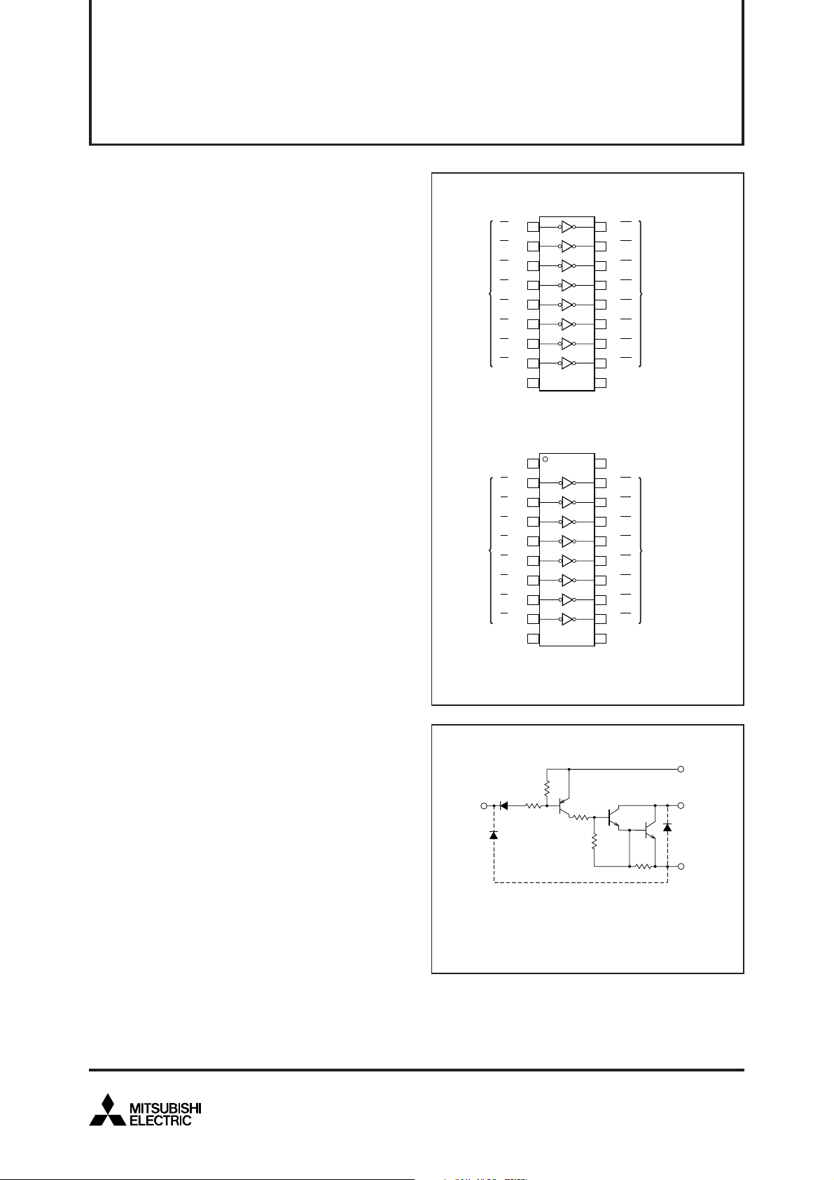
PIN CONFIGURATION (TOP VIEW)
M54583P
1IN1→
2
IN2→
3
IN3→
4
INPUT OUTPUT
IN4→
IN5→
IN6→
IN7→
IN8→
GND
5
6
7
8
9
→O1
18
→O2
17
→O3
16
→O4
15
→O5
14
→O6
13
→O7
12
→O8
11
CC
V
10
Outline 18P4G
M54583FP
INPUT
IN1→
IN2→
IN3→
IN4→
IN5→
IN6→
IN7→
IN8→
GND
1NC
2
3
4
5
6
7
8
9
10 11
20
NC
→O1
19
→O2
18
→O3
17
→O4
16
→O5
15
→O6
14
→O7
13
→O8
12
V
CC
Outline 20P2N-A
NC : No connection
CIRCUIT DIAGRAM (EACH CIRCUIT)
7k
INPUT
7k
2.7k
7.2k
OUTPUT
3k
CC
V
OUTPUT
GND
The eight circuits share the V
The diode, indicated with the dotted line, is parasitic, and cannot
be used.
CC
and GND.
Unit : Ω
May 2007

MITSUBISHI SEMICONDUCTOR <TRANSISTOR ARRAY>
8-UNIT 400mA DARLINGTON TRANSISTOR ARRAY
ABSOLUTE MAXIMUM RATINGS (Unless otherwise noted, Ta = –20 ~ +75°C)
CC
V
VCEO
VI
IC
Pd
Topr
Tstg
RECOMMENDED OPERATING CONDITIONS (Unless otherwise noted, Ta = –20 ~ +75°C)
Symbol
CC
V
IC
VIH
VIL
Supply voltage
Collector-emitter voltage
Input voltage
Collector current
Power dissipation
Operating temperature
Storage temperature
Parameter
Supply voltage
CC = 5V, Duty Cycle
V
P : no more than 10%
Collector current
Per channel
FP : no more than 5%
V
CC = 5V, Duty Cycle
P : no more than 34%
FP : no more than 15%
“H” input voltage
“L” input voltage
Output, H
Current per circuit output, L
Ta = 25°C, when mounted on board
Limits
min typ max
4
0
5
—
Unit
8
350
mA
200
V
CC
VCC–3.6
V
CC–0.7
0
—
—
0
—
V
V
V
M54583P/FP
Ratings
10
–0.5 ~ +50
–0.5 ~ VCC
400
1.79/1.1
–20 ~ +75
–55 ~ +125
UnitSymbol Parameter Conditions
V
V
V
mA
W
°C
°C
ELECTRICAL CHARACTERISTICS (Unless otherwise noted, Ta = –20 ~ +75°C)
Symbol UnitParameter Test conditions
V
(BR) CEO
CE (sat)
V
II
ICC
hFE
+ : The typical values are those measured under ambient temperature (Ta) of 25°C. There is no guarantee that these values are obtained under any
conditions.
Collector-emitter breakdown voltage
Collector-emitter saturation voltage
Input current
Supply current (one circuit coming on)
DC amplification factor
ICEO = 100µA, VCC = 8V
VI = VCC–3.6V
IC = 350mA
IC = 200mA
VI = VCC–3.6V
VCC = 5V, VI = VCC–3.6V
VCE = 4V, VCC = 5V, IC = 350mA, Ta = 25°C
min typ
2000
Limits
+
max
1.2
1.9
—
2.2
1.6
–600
—
V
V
µA
3
mA
—
50
—
—
—
—
0.98
–320
—
3500
SWITCHING CHARACTERISTICS (Unless otherwise noted, Ta = 25°C)
Symbol UnitParameter Test conditions
ton
toff
NOTE 1 TEST CIRCUIT
Turn-on time
Turn-off time
V
INPUT
PG
50Ω C
CC
Measured
device
CL = 15pF (note 1)
V
O
R
L
OUTPUT
L
TIMING DIAGRAM
INPUT
OUTPUT
min typ max
50% 50%
50% 50%
Limits
—
—
130
3200
—
—
ns
ns
(1) Pulse generator (PG) characteristics : PRR = 1kHz,
tw = 10µs, tr = 6ns, tf = 6ns, Z
I
= 0.4 to 4V
V
(2) Input-output conditions : R
(3) Electrostatic capacity C
connections and input capacitance at probes
O
= 50Ω
L
= 30Ω, VO = 10V, VCC = 4V
L
includes floating capacitance at
ton
toff
May 2007
2

TYPICAL CHARACTERISTICS
Thermal Derating Factor Characteristics
2.0
M54583P
MITSUBISHI SEMICONDUCTOR <TRANSISTOR ARRAY>
M54583P/FP
8-UNIT 400mA DARLINGTON TRANSISTOR ARRAY
Output Saturation Voltage
Collector Current Characteristics
500
1.5
M54583FP
1.0
0.5
Power dissipation Pd (W)
0
0
25 50 75 100
Ambient temperature Ta (°C)
Duty-Cycle-Collector Characteristics
(M54583P)
500
400
300
200
•The collector current values
represent the current per circuit.
Collector current Ic (mA)
•Repeated frequency ≥ 10Hz
100
•The value in the circle represents the
value of the simultaneously-operated circuit.
CC
= 5V
•V
•Ta = 25°C
0
020406080100
1
2
3
4
5
6
8
7
400
300
200
Collector current Ic (mA)
100
0
0 2.00.5 1.0 1.5
VI = 1.4V
CC
V
Output saturation voltage V
Duty-Cycle-Collector Characteristics
(M54583P)
500
400
300
200
•The collector current values
Collector current Ic (mA)
represent the current per circuit.
100
•Repeated frequency
•The value in the circle represents the
value of the simultaneously-operated circuit.
CC
= 5V •Ta = 75°C
•V
0
020406080100
≥
10Hz
= 5V
Ta = 75°C
Ta = 75°C
Ta = 25°C
Ta = 25°C
Ta = –20°C
Ta = –20°C
CE
(sat) (V)
1
2
3
4
5
7
6
8
Duty cycle (%)
Duty-Cycle-Collector Characteristics
(M54583FP)
500
400
300
200
•The collector current values
represent the current per circuit.
Collector current Ic (mA)
100
•Repeated frequency ≥ 10Hz
•The value in the circle represents the
value of the simultaneously-operated circuit.
•V
CC
= 5V •Ta = 25°C
0
020406080100
Duty cycle (%)
1
2
3
4
5
6
7
8
Duty-Cycle-Collector Characteristics
500
400
300
200
Collector current Ic (mA)
•The collector current values
100
represent the current per circuit.
•Repeated frequency
•The value in the circle represents the
value of the simultaneously-operated circuit.
0
020406080100
3
Duty cycle (%)
(M54583FP)
≥
10Hz
Duty cycle (%)
•Vcc =5.0V
•Ta = 75°C
1
2
3
4
5
6
7
8
May 2007

MITSUBISHI SEMICONDUCTOR <TRANSISTOR ARRAY>
M54583P/FP
8-UNIT 400mA DARLINGTON TRANSISTOR ARRAY
Input Characteristics
–1.0
–0.8
VCC = 5V
Ta = 75°C
(mA)
I
–0.6
Ta = 75°C
Ta = 25°C
Ta = 25°C
Ta = –20°C
Ta = –20°C
–0.4
Input current I
–0.2
0
012345
Supply voltage-Input voltage V
Grounded Emitter Transfer Characteristics
400
VCC = 4V
CE
= 4V
V
300
Ta = 75°C
Ta = 25°C
Ta = –20°C
200
CC–VI
(V)
DC Amplification Factor
Collector Current Characteristics
4
10
7
5
FE
3
3
10
7
5
3
DC amplification factor h
2
10
1
10
357
Collector current Ic (mA)
Supply Current Characteristics
5
VI = 0V
Ta = 75°C
4
Ta = 75°C
Ta = 25°C
Ta = 25°C
Ta = –20°C
Ta = –20°C
3
2
10
VCC = 5V
CE
V
2
= 4V
Ta = 75°C
Ta = 75°C
Ta = 25°C
Ta = 25°C
Ta = –20°C
Ta = –20°C
357
10
3
100
Collector current Ic (mA)
0
0
01234
Supply voltage-Input voltage V
CC–VI
(V)
Supply current Icc (mA)
1
0
0246810
Supply voltage V
CC
(V)
May 2007
4
 Loading...