

Mitsubishi M34514M8-XXXFP, M34514M6-XXXFP, M34514E8FP, M34513M8-XXXFP, M34513M6-XXXFP Datasheet
...
MITSUBISHI MICROCOMPUTERS
4513/4514 Group
PRELIMINARY
Notice: This is not a final specification.
Some parametric limits are subject to
change.
SINGLE-CHIP 4-BIT CMOS MICROCOMPUTER
DESCRIPTION
The 4513/4514 Group is a 4-bit single-chip microcomputer designed with CMOS technology. Its CPU is that of the 4500 series
using a simple, high-speed instruction set. The computer is
equipped with serial I/O, four 8-bit timers (each timer has a reload
register), and 10-bit A-D converter.
The various microcomputers in the 4513/4514 Group include variations of the built-in memory type and package as shown in the
table below.
FEATURES
●Minimum instruction execution time ................................ 0.75 µs
(at 4.0 MHz oscillation frequency, in high-speed mode, VDD = 4.0
V to 5.5 V)
● Supply voltage
• Middle-speed mode
...... 2.5 V to 5.5 V (at 4.2 MHz oscillation frequency, for Mask
ROM version and One Time PROM version)
...... 2.0 V to 5.5 V (at 3.0 MHz oscillation frequency, for Mask
ROM version)
(Operation voltage of A-D conversion: 2.7 V to 5.5 V)
• High-speed mode
...... 4.0 V to 5.5 V (at 4.2 MHz oscillation frequency, for Mask
ROM version and One Time PROM version)
...... 2.5 V to 5.5 V (at 2.0 MHz oscillation frequency, for Mask
ROM version and One Time PROM version)
...... 2.0 V to 5.5 V (at 1.5 MHz oscillation frequency, for Mask
ROM version)
(Operation voltage of A-D conversion: 2.7 V to 5.5 V)
● Timers
Timer 1...................................... 8-bit timer with a reload register
Timer 2...................................... 8-bit timer with a reload register
Timer 3...................................... 8-bit timer with a reload register
Timer 4...................................... 8-bit timer with a reload register
● Interrupt ........................................................................ 8 sources
● Serial I/O ....................................................................... 8 bit-wide
● A-D converter ..................10-bit successive comparison method
● Voltage comparator ........................................................2 circuits
● Watchdog timer ................................................................. 16 bits
● Voltage drop detection circuit
● Clock generating circuit (ceramic resonator)
● LED drive directly enabled (port D)
APPLICATION
Microwave oven, rice cooker, audio, telephone, office equipment
Product
M34513M2-XXXSP/FP *
M34513M4-XXXSP/FP *
M34513E4SP/FP * (Note)
M34513M6-XXXFP **
M34513M8-XXXFP **
M34513E8FP ** (Note)
M34514M6-XXXFP *
M34514M8-XXXFP *
M34514E8FP * (Note)
Note: shipped in blank
* : Under development
**: Under planning
ROM (PROM) size
(✕ 10 bits)
2048 words
4096 words
4096 words
6144 words
8192 words
8192 words
6144 words
8192 words
8192 words
RAM size
(✕ 4 bits)
128 words
256 words
256 words
384 words
384 words
384 words
384 words
384 words
384 words
Package
SP: 32P4B FP: 32P6B-A
SP: 32P4B FP: 32P6B-A
SP: 32P4B FP: 32P6B-A
32P6B-A
32P6B-A
32P6B-A
42P2R-A
42P2R-A
42P2R-A
ROM type
Mask ROM
Mask ROM
One Time PROM
Mask ROM
Mask ROM
One Time PROM
Mask ROM
Mask ROM
One Time PROM
PRELIMINARY
Notice: This is not a final specification.
Some parametric limits are subject to
change.
PIN CONFIGURATION (TOP VIEW) 4513 Group
MITSUBISHI MICROCOMPUTERS
4513/4514 Group
SINGLE-CHIP 4-BIT CMOS MICROCOMPUTER
D
D
D
D
D
D
D6/CNTR0
D
7
/CNTR1
0/SCK
P2
P21/S
OUT
P22/S
IN
RESET
SS
CNV
X
OUT
X
IN
V
SS
1
0
1
2
2
3
3
4
5
4
6
5
7
8
9
10
11
12
13
14
15
16
M34513E4SP
M34513Mx-XXXSP
32
31
30
29
28
27
26
25
24
23
22
21
20
19
18
17
P1
3
P1
2
P1
1
P1
0
P0
3
P0
2
P0
1
P0
0
A
IN3
/CMP1+
A
IN2
/CMP1-
IN1
/CMP0+
A
A
IN0
/CMP0-
1
/INT1
P3
P30/INT0
VDCE
DD
V
Outline 32P4B
D6/CNTR
D7/CNTR
P20/S
P21/S
OUT
P22/S
D
D
D
CK
3
0
2
P13P1
28
29
13
12
IN
SS
X
V
1
P1
27
14
DD
V
P0
P1
25
26
16
15
/INT0
VDCE
0
P3
24
23
22
21
20
19
18
17
P0
P0
P0
A
A
A
A
P3
IN3
IN2
IN1
IN0
2
1
0
/CMP1+
/CMP1-
/CMP0+
/CMP0-
1
/INT1
0
2
1
D
D
D
32
30
31
3
1
2
4
5
3
M34513Mx-XXXFP
4
0
5
1
6
7
IN
8
M34513ExFP
9
11
10
SS
OUT
X
RESET
CNV
Outline 32P6B-A
2
PRELIMINARY
Notice: This is not a final specification.
Some parametric limits are subject to
change.
PIN CONFIGURATION (TOP VIEW) 4514 Group
MITSUBISHI MICROCOMPUTERS
4513/4514 Group
SINGLE-CHIP 4-BIT CMOS MICROCOMPUTER
P1
D
D
D
D
D
D
D6/CNTR0
D
7
/CNTR1
P5
P5
P5
P5
P20/S
CK
P2
1/SOUT
P22/S
IN
RESET
CNV
SS
X
OUT
X
IN
V
SS
1
3
2
0
3
1
4
2
5
3
6
4
7
5
8
9
10
0
11
1
12
2
13
3
14
15
16
17
18
19
20
21
M34514E8FP
M34514Mx-XXXFP
42
41
40
39
38
37
36
35
34
33
32
31
30
29
28
27
26
25
24
23
22
P1
2
P1
1
P1
0
P0
3
P0
2
P0
1
P0
0
P43/A
P42/A
P41/A
P40/A
A
IN3
/CMP1+
A
IN2
/CMP1-
A
IN1
/CMP0+
A
IN0
/CMP0-
P3
3
P3
2
P3
1
/INT1
P3
0
/INT0
VDCE
DD
V
IN7
IN6
IN5
IN4
Outline 42P2R-A
3
|[go1
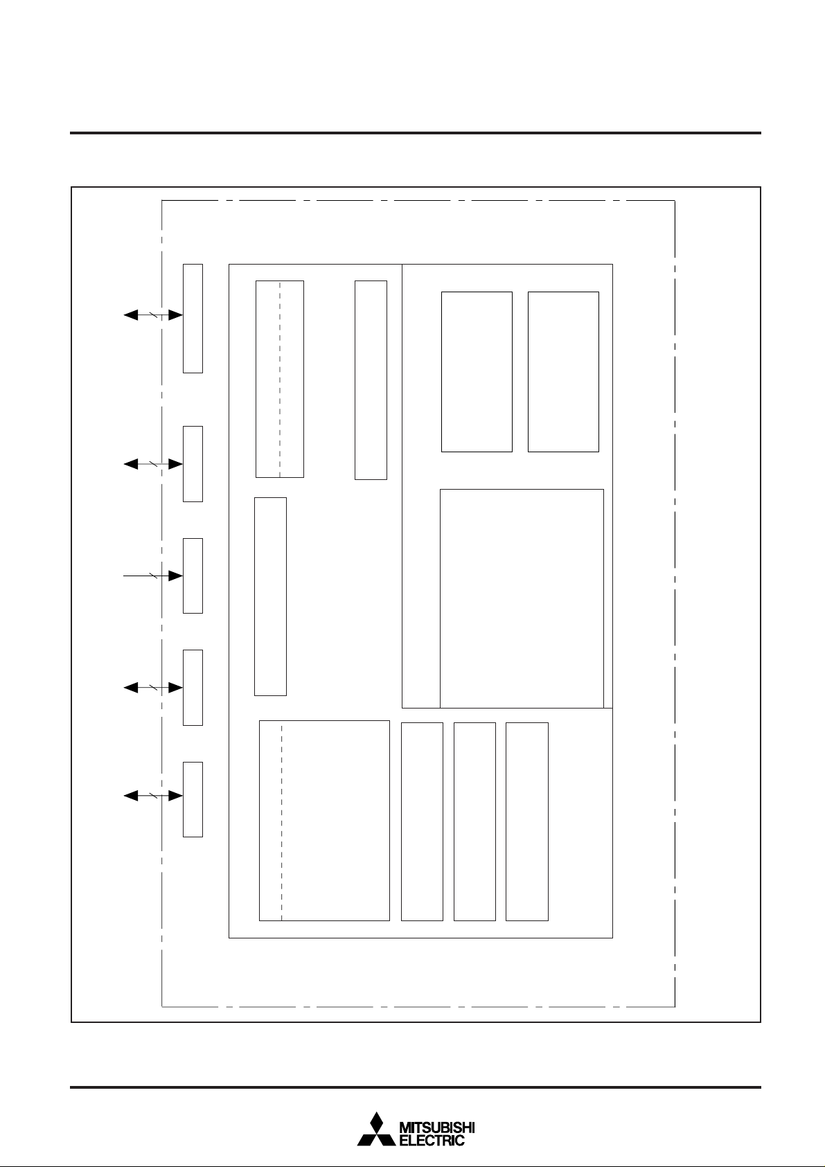
Voltage drop detection circuit
4
Serial I/O
(8 bits ✕ 1)
Voltage comparator
(2 circuits)
X
IN
–X
OUT
I/O port
Internal peripheral functions
Timer
System clock generating circuit
Watchdog timer
(16 bits)
Memory
ROM
2048, 4096,6144, 8192
words × 10 bits
RAM
128, 256, 384 words × 4 bits
4500 Series
CPU core
ALU (4 bits)
Register A (4 bits) Register B (4 bits)
Register D (3 bits) Register E (8 bits)
Stack register SK (8 levels)
Interrupt stack register SDP (1 level)
Timer 1 (8 bits)
Timer 2 (8 bits)
Timer 3 (8 bits)
Timer 4 (8 bits)
A-D converter
(10 bits ✕ 4 ch)
Port D
Port P3
Port P2
Port P1
Port P0
4
3
2
8
MITSUBISHI MICROCOMPUTERS
4513/4514 Group
PRELIMINARY
Notice: This is not a final specification.
Some parametric limits are subject to
change.
BLOCK DIAGRAM (4513 Group)
SINGLE-CHIP 4-BIT CMOS MICROCOMPUTER
4
PRELIMINARY
Voltage drop detection circuit
Serial I/O
(8 bits ✕ 1)
Voltage comparator
(2 circuits)
X
IN
—X
OUT
I/O port
Internal peripheral functions
Timer
System clock generating circuit
Watchdog timer
(16 bits)
Memory
ROM
6144, 8192 words × 10 bits
RAM
384 words × 4 bits
4500 Series
CPU core
ALU (4 bits)
Register A (4 bits) Register B (4 bits)
Register D (3 bits) Register E (8 bits)
Stack register SK (8 levels)
Interrupt stack register SDP (1 level)
Timer 1 (8 bits)
Timer 2 (8 bits)
Timer 3 (8 bits)
Timer 4 (8 bits)
A-D converter
(10 bits ✕ 8 ch)
Port DPort P3Port P2Port P1Port P0 Port P5Port P4
4
4
4
4
4
8
3
Notice: This is not a final specification.
Some parametric limits are subject to
change.
BLOCK DIAGRAM (4514 Group)
MITSUBISHI MICROCOMPUTERS
4513/4514 Group
SINGLE-CHIP 4-BIT CMOS MICROCOMPUTER
5
PRELIMINARY
Notice: This is not a final specification.
Some parametric limits are subject to
change.
PERFORMANCE OVERVIEW
Parameter
Number of
basic instructions
Minimum instruction execution time
Memory sizes
Input/Output
ports
Timers
A-D converter
Voltage comparator
Serial I/O
Interrupt
Subroutine nesting
Device structure
Package
Operating temperature range
Supply voltage
Power
dissipation
(typical value)
ROM
RAM
D0–D7
P00–P03
P10–P13
P20–P22
P30–P33
P40–P43
P50–P53
CNTR0
CNTR1
INT0
INT1
Timer 1
Timer 2
Timer 3
Timer 4
Sources
Nesting
4513 Group
4514 Group
Active mode
RAM back-up mode
4513 Group
4514 Group
M34513M2
M34513M4/E4
M34513M6
M34513M8/E8
M34514M6
M34514M8/E8
M34513M2
M34513M4/E4
M34513M6
M34513M8/E8
M34514M6
M34514M8/E8
I/O (Input is
examined by
skip decision)
I/O
I/O
Input
I/O
I/O
I/O
I/O
I/O
Input
Input
MITSUBISHI MICROCOMPUTERS
4513/4514 Group
SINGLE-CHIP 4-BIT CMOS MICROCOMPUTER
Function
123
128
0.75 µs (at 4.0 MHz oscillation frequency, in high-speed mode)
2048 words ✕ 10 bits
4096 words ✕ 10 bits
6144 words ✕ 10 bits
8192 words ✕ 10 bits
6144 words ✕ 10 bits
8192 words ✕ 10 bits
128 words ✕ 4 bits
256 words ✕ 4 bits
384 words ✕ 4 bits
384 words ✕ 4 bits
384 words ✕ 4 bits
384 words ✕ 4 bits
Eight independent I/O ports;
ports D6 and D7 are also used as CNTR0 and CNTR1, respectively.
4-bit I/O port; each pin is equipped with a pull-up function and a key-on wakeup function. Both
functions can be switched by software.
4-bit I/O port; each pin is equipped with a pull-up function and a key-on wakeup function. Both
functions can be switched by software.
3-bit input port; ports P20, P21 and P22 are also used as SCK, SOUT and SIN, respectively.
4-bit I/O port (2-bit I/O port for the 4513 Group); ports P30 and P31 are also used as INT0 and
INT1, respectively. The 4513 Group does not have ports P32, P33.
4-bit I/O port; The 4513 Group does not have this port.
4-bit I/O port with a direction register; The 4513 Group does not have this port.
1-bit I/O; CNTR0 pin is also used as port D6.
1-bit I/O; CNTR1 pin is also used as port D7.
1-bit input; INT0 pin is also used as port P30 and equipped with a key-on wakeup function.
1-bit input; INT1 pin is also used as port P31 and equipped with a key-on wakeup function.
8-bit programmable timer with a reload register.
8-bit programmable timer with a reload register is also used as an event counter.
8-bit programmable timer with a reload register.
8-bit programmable timer with a reload register is also used as an event counter.
10-bit wide, This is equipped with an 8-bit comparator function.
2 circuits (CMP0, CMP1)
8-bit ✕ 1
8 (two for external, four for timer, one for A-D, and one for serial I/O)
1 level
8 levels
CMOS silicon gate
32-pin plastic molded SDIP (32P4B)/LQFP(32P6B-A)
42-pin plastic molded SSOP (42P2R-A)
–20 °C to 85 °C
2.0 V to 5.5 V for Mask ROM version, 2.5 V to 5.5 V for One Time PROM version (Refer to the
electrical characteristics because the supply voltage depends on the oscillation frequency.)
1.8 mA (at VDD = 5.0 V, 4.0 MHz oscillation frequency, in middle- speed mode, output transis-
tors in the cut-off state)
3.0 mA (at VDD = 5.0 V, 4.0 MHz oscillation frequency, in high-speed mode, output transistors
in the cut-off state)
0.1 µA (at room temperature, VDD = 5 V, output transistors in the cut-off state)
6
PRELIMINARY
Notice: This is not a final specification.
Some parametric limits are subject to
change.
PIN DESCRIPTION
Pin
VDD
VSS
VDCE
CNVSS
RESET
XIN
XOUT
D0–D7
P00–P03
P10–P13
P20–P22
P30–P33
P40–P43
P50–P53
AIN0–AIN7
CNTR0
CNTR1
INT0, INT1
SIN
SOUT
SCK
CMP0CMP0+
CMP1CMP1+
Name
Power supply
Ground
Voltage drop detec-
tion circuit enable
CNVSS
Reset input
System clock input
System clock output
I/O port D
(Input is examined
by skip decision.)
I/O port P0
I/O port P1
Input port P2
I/O port P3
I/O port P4
I/O port P5
Analog input
Timer input/output
Timer input/output
Interrupt input
Serial data input
Serial data output
Serial I/O clock
input/output
Voltage comparator
input
Voltage comparator
input
Input/Output
—
—
Input
—
I/O
Input
Output
I/O
I/O
I/O
Input
I/O
I/O
I/O
Input
I/O
I/O
Input
Input
Output
I/O
Input
Input
MITSUBISHI MICROCOMPUTERS
4513/4514 Group
SINGLE-CHIP 4-BIT CMOS MICROCOMPUTER
Function
Connected to a plus power supply.
Connected to a 0 V power supply.
VDCE pin is used to control the operation/stop of the voltage drop detection circuit.
When “H” level is input to this pin, the circuit is operating. When “L” level is inpu to
this pin, the circuit is stopped.
Connect CNVSS to VSS and apply “L” (0V) to CNVSS certainly.
An N-channel open-drain I/O pin for a system reset. When the watchdog timer
causes the system to be reset or system reset is performed by the voltage drop detection circuit, the RESET pin outputs “L” level.
I/O pins of the system clock generating circuit. XIN and XOUT can be connected to
ceramic resonator. A feedback resistor is built-in between them.
Each pin of port D has an independent 1-bit wide I/O function. Each pin has an output latch. For input use, set the latch of the specified bit to “1.” The output structure
is N-channel open-drain.
Ports D6 and D7 are also used as CNTR0 and CNTR1, respectively.
Each of ports P0 and P1 serves as a 4-bit I/O port, and it can be used as inputs
when the output latch is set to “1.” The output structure is N-channel open-drain.
Every pin of the ports has a key-on wakeup function and a pull-up function. Both
functions can be switched by software.
3-bit input port. Ports P20, P21 and P22 are also used as SCK, SOUT and SIN, respectively.
4-bit I/O port (2-bit I/O port for the 4513 Group). For input use, set the latch of the
specified bit to “1.” The output structure is N-channel open-drain. Ports P30 and
P31 are also used as INT0 and INT1, respectively.
The 4513 Group does not have ports P32, P33.
4-bit I/O port. For input use, set the latch of the specified bit to “1.” The output
structure is N-channel open-drain. Ports P40–P43 are also used as analog input
pins AIN4–AIN7, respectively.
The 4513 Group does not have port P4.
4-bit I/O port. Each pin has a direction register and an independent 1-bit wide I/O
function. For input use, set the direction register to “0.” For output use, set the direction regiser to “1.” The output structure is CMOS.
The 4513 Group does not have port P5.
Analog input pins for A-D converter. AIN0–AIN3 are also used as comparator input
pins and AIN4–AIN7 are also used as port P4.
The 4513 Group does not have AIN4–AIN7.
CNTR0 pin has the function to input the clock for the timer 2 event counter, and to
output the timer 1 underflow signal divided by 2.
CNTR0 pin is also used as port D6.
CNTR1 pin has the function to input the clock for the timer 4 event counter, and to
output the timer 3 underflow signal divided by 2.
CNTR1 pin is also used as port D7.
INT0, INT1 pins accept external interrupts. They also accept the input signal to return the system from the RAM back-up state.
INT0, INT1 pins are also used as ports P30 and P31, respectively.
SIN pin is used to input serial data signals by software.
SIN pin is also used as port P22.
SOUT pin is used to output serial data signals by software.
SOUT pin is also used as port P21.
SCK pin is used to input and output synchronous clock signals for serial data transfer by software.
SCK pin is also used as port P20.
CMP0-, CMP0+ pins are used as the voltage comparator input pin when the voltage comparator function is selected by software.
CMP0-, CMP0+ pins are also used as AIN0 and AIN1.
CMP1-, CMP1+ pins are used as the voltage comparator input pin when the voltage comparator function is selected by software.
CMP1-, CMP1+ pins are also used as AIN2 and AIN3.
7
PRELIMINARY
Notice: This is not a final specification.
Some parametric limits are subject to
change.
MULTIFUNCTION
Pin
D6
D7
P20
P21
P22
P30
P31
Notes 1: Pins except above have just single function.
2: The input of D
S
3: The 4513 Group does not have P4
Multifunction
CNTR0
CNTR1
SCK
SOUT
SIN
INT0
INT1
6, D7, P20–P22, CMP0-, CMP0+, CMP1-, CMP1+ and the input/output of P30, P31, P40–P43 can be used even when CNTR0, CNTR1,
CK, SOUT, SIN, INT0, INT1, and AIN0–AIN7 are selected.
CONNECTIONS OF UNUSED PINS
Pin
XOUT
VDCE
D0–D5
D6/CNTR0
D7/CNTR1
P20/SCK
P21/SOUT
P22/SIN
P30/INT0
P31/INT1
P32, P33
P40/AIN4–P43/AIN7
P50–P53 (Note 1)
AIN0/CMP0AIN1/CMP0+
AIN2/CMP1AIN3/CMP1+
P00–P03
P10–P13
Open (when using an external clock).
Connect to VSS.
Connect to VSS, or set the output latch to
“0” and open.
Connect to VSS.
Connect to VSS, or set the output latch to
“0” and open.
Connect to VSS, or set the output latch to
“0” and open.
When the input mode is selected by software, pull-up to VDD through a resistor or
pull-down to VDD.
When selecting the output mode, open.
Connect to VSS.
Open or connect to VSS (Note 2)
Open or connect to VSS (Note 2)
Pin
CNTR0
CNTR1
SCK
SOUT
SIN
INT0
INT1
0/AIN4–P43/AIN7.
Connection
Multifunction
D6
D7
P20
P21
P22
P30
P31
MITSUBISHI MICROCOMPUTERS
4513/4514 Group
SINGLE-CHIP 4-BIT CMOS MICROCOMPUTER
Pin
AIN0
AIN1
AIN2
AIN3
P40
P41
P42
P43
Notes 1: After system is released from reset, port P5 is in a input mode (di-
2: When the P0
(Note when the output latch is set to “0” and pins are open)
● After system is released from reset, port is in a high-impedance state un-
til it is set the output latch to “0” by software. Accordingly, the voltage
level of pins is undefined and the excess of the supply current may occur
while the port is in a high-impedance state.
● To set the output latch periodically by software is recommended because
value of output latch may change by noise or a program run away
(caused by noise).
(Note when connecting to V
● Connect the unused pins to V
shortest distance against noise.
Multifunction
CMP0CMP0+
CMP1CMP1+
AIN4
AIN5
AIN6
AIN7
rection register FR0 = 0000
0–P03 and P10–P13 are connected to VSS, turn off
their pull-up transistors (register PU0i=“0”) and also invalidate the
key-on wakeup functions (register K0i=“0”) by software. When
these pins are connected to V
tions are left valid, the system fails to return from RAM back-up
state. When these pins are open, turn on their pull-up transistors
(register PU0i=“1”) by software, or set the output latch to “0.”
Be sure to select the key-on wakeup functions and the pull-up
functions with every two pins. If only one of the two pins for the
key-on wakeup function is used, turn on their pull-up transistors by
software and also disconnect the other pin. (i = 0, 1, 2, or 3.)
SS and VDD)
Pin
CMP0CMP0+
CMP1CMP1+
AIN4
AIN5
AIN6
AIN7
2)
SS while the key-on wakeup func-
SS and VDD using the thickest wire at the
Multifunction
AIN0
AIN1
AIN2
AIN3
P40
P41
P42
P43
8
PRELIMINARY
Notice: This is not a final specification.
Some parametric limits are subject to
change.
PORT FUNCTION
Port
Port D
Port P0
Port P1
Port P2
Port P3
(Note 1)
Port P4
(Note 2)
Port P5
(Note 2)
Notes 1: The 4513 Group does not have P32 and P33.
2: The 4513 Group does not have these ports.
Pin
D0–D5
D6/CNTR0
D7/CNTR1
P00–P03
P10–P13
P20/SCK
P21/SOUT
P22/SIN
P30/INT0
P31/INT1
P32, P33
P40/AIN4
–P43/AIN7
P50–P53
Input
Output
I/O
(8)
I/O
(4)
I/O
(4)
Input
(3)
I/O
(4)
I/O
(4)
I/O
(4)
N-channel open-drain
N-channel open-drain
N-channel open-drain
N-channel open-drain
N-channel open-drain
CMOS
Output structure
I/O
unit
1
4
4
3
4
4
4
MITSUBISHI MICROCOMPUTERS
4513/4514 Group
SINGLE-CHIP 4-BIT CMOS MICROCOMPUTER
Control
instructions
SD, RD
SZD
CLD
OP0A
IAP0
OP1A
IAP1
IAP2
OP3A
IAP3
OP4A
IAP4
OP5A
IAP5
Control
registers
W6
PU0, K0
PU0, K0
J1
I1, I2
Q2
FR0
Remark
Built-in programmable pull-up
functions
Key-on wakeup functions
(programmable)
Built-in programmable pull-up
functions
Key-on wakeup functions
(programmable)
Built-in key-on wakeup
function
(P30/INT0, P31/INT1)
DEFINITION OF CLOCK AND CYCLE
● System clock
The system clock is the basic clock for controlling this product.
The system clock is selected by the bit 3 of the clock control register MR.
Table Selection of system clock
Register MR
MR3
0
1
Note: f(XIN)/2 is selected after system is released from reset.
● Instruction clock
The instruction clock is a signal derived by dividing the system
clock by 3. The one instruction clock cycle generates the one
machine cycle.
● Machine cycle
The machine cycle is the standard cycle required to execute the
instruction.
System clock
f(XIN)
f(XIN)/2
9
PRELIMINARY
Notice: This is not a final specification.
Some parametric limits are subject to
change.
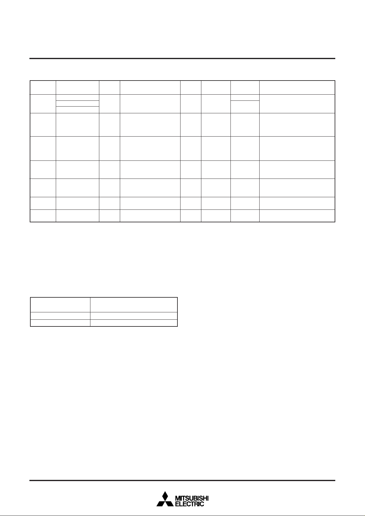
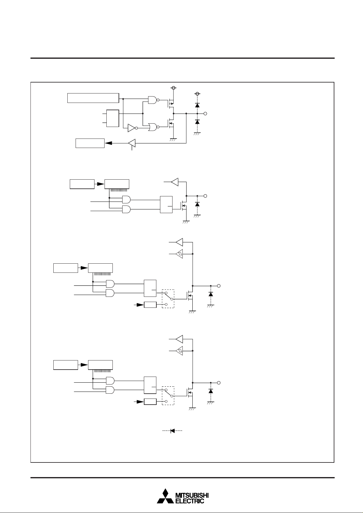
PORT BLOCK DIAGRAMS
Key-on wakeup input
K0
0
IAP0 instruction
Pull-up
transistor
PU0
0
MITSUBISHI MICROCOMPUTERS
4513/4514 Group
SINGLE-CHIP 4-BIT CMOS MICROCOMPUTER
Register A
OP0A instruction
Key-on wakeup input
Register A
OP0A instruction
Key-on wakeup input
DTQAi
K0
1
IAP0 instruction
DTQAi
K0
2
IAP1 instruction
Pull-up
transistor
PU0
1
Pull-up
transistor
PU0
2
P00,P0
P02,P0
1
3
Register A
OP1A instruction
Key-on wakeup input
Register A
OP1A instruction
DTQAi
K0
3
IAP1 instruction
DTQAi
Pull-up
transistor
PU0
3
•
i represents 0, 1, 2, or 3.
•
This symbol represents a parasitic diode on the port.
P10,P1
P12,P1
1
3
10
PRELIMINARY
Notice: This is not a final specification.
Some parametric limits are subject to
change.
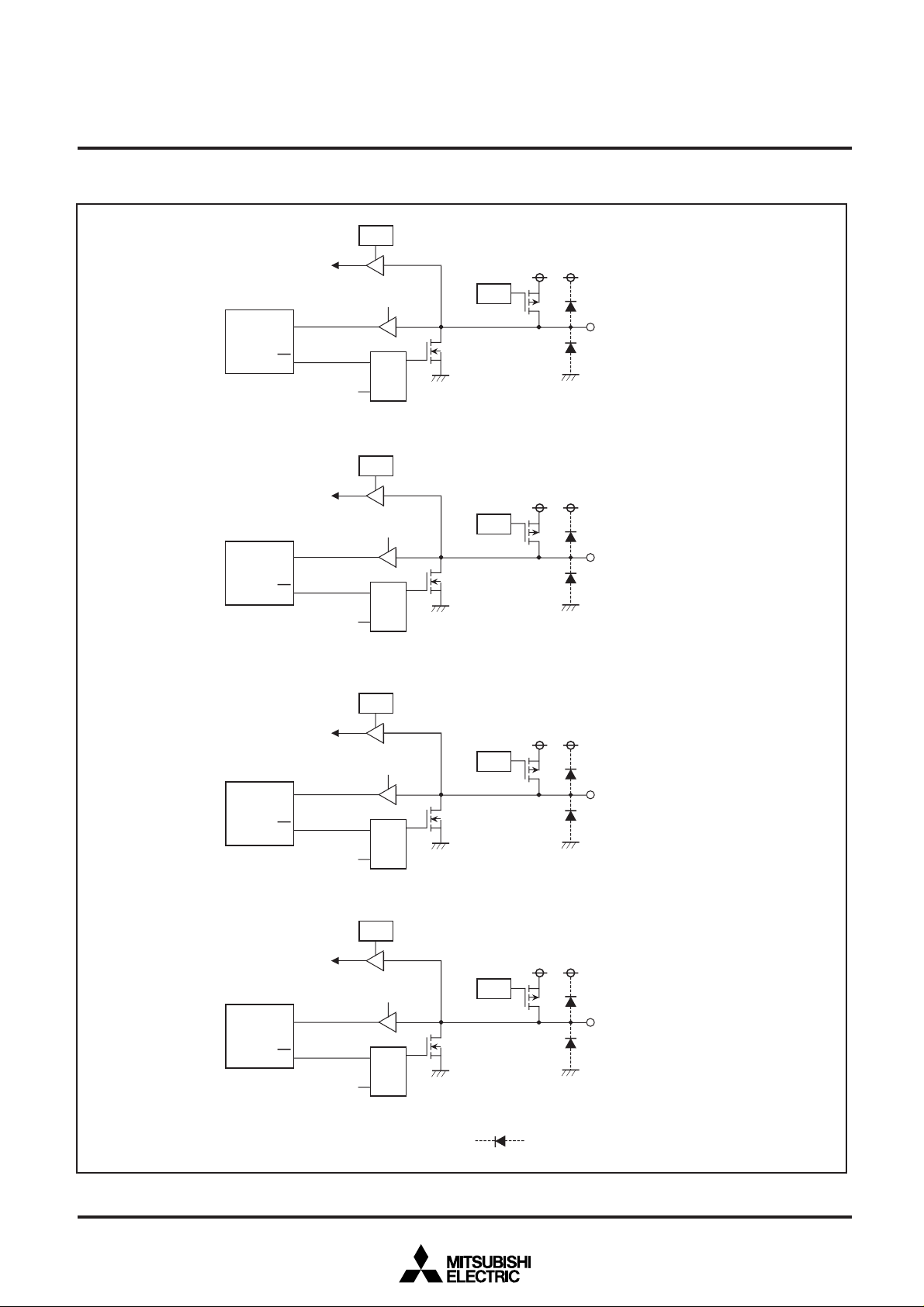
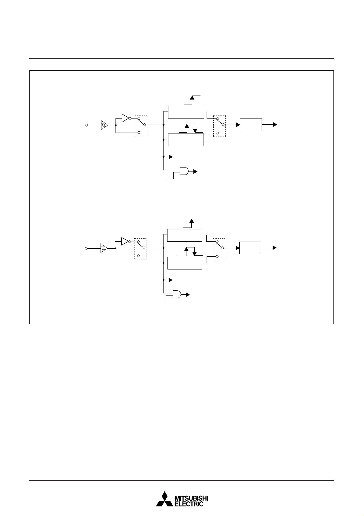
PORT BLOCK DIAGRAMS (continued)
Synchronous clock input for serial transfer
Synchronous clock output for serial transfer
J1
Register A
0
Register A
SINGLE-CHIP 4-BIT CMOS MICROCOMPUTER
IAP2 instruction
J1
1
0
1
IAP2 instruction
MITSUBISHI MICROCOMPUTERS
4513/4514 Group
P20/S
CK
Serial data output
Register A
Key-on wakeup input
External interrupt circuit
Register A
Ai
OP3A instruction
Register A
Serial data input
IAP2 instruction
IAP3 instruction
DTQ
IAP3 instruction
J1
1
0
1
P21/S
P22/S
OUT
IN
P30/INT0,P31/INT1
P32,P3
3
Ai
OP3A instruction
•
• Applied potential to ports P2
• i represents 0, 1, 2, or 3.
• The 4513 Group does not have ports P3
This symbol represents a parasitic diode on the port.
DTQ
0
—P22 must be VDD.
2
, P33.
11
PRELIMINARY
Notice: This is not a final specification.
Some parametric limits are subject to
change.
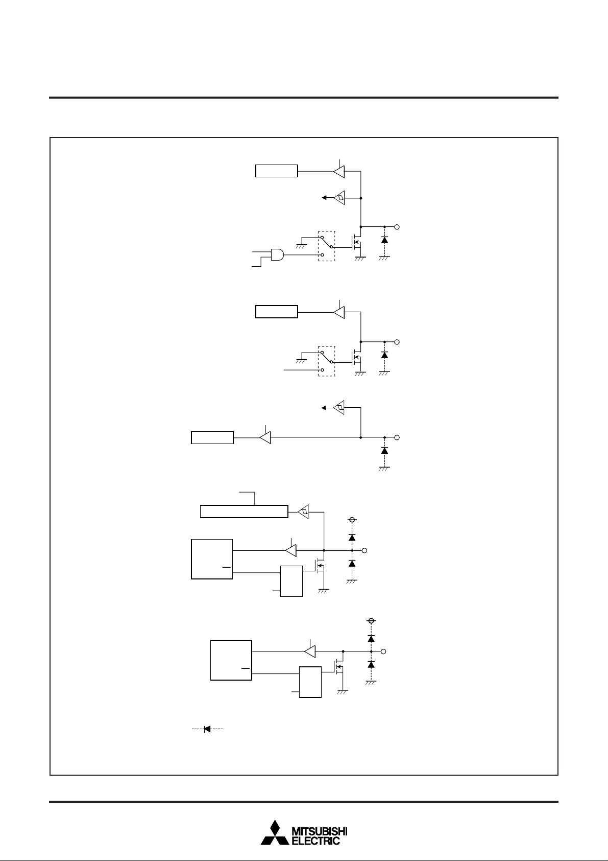
PORT BLOCK DIAGRAMS (continued)
MITSUBISHI MICROCOMPUTERS
4513/4514 Group
SINGLE-CHIP 4-BIT CMOS MICROCOMPUTER
Q1
Decoder
Analog input
Q3
0
CMP0
Analog input
Analog input
Q3
1
CMP1
Q3
Q3
A
IN0
/CMP0-
-
+
2
Q1
Decoder
A
IN1
/CMP0+
Q1
Decoder
A
IN2
/CMP1-
-
+
3
Q1
Analog input
Register A
Ai
OP4A instruction
Analog input
IAP4 instruction
DQ
T
Decoder
Q1
Decoder
A
IN3
/CMP1+
P40/A
IN4
–P43/A
IN7
•
• i represents 0, 1, 2, or 3.
• The 4513 Group does not have port P4.
This symbol represents a parasitic diode on the port.
12
PRELIMINARY
Notice: This is not a final specification.
Some parametric limits are subject to
change.
PORT BLOCK DIAGRAMS (continued)
Direction register FR0i
DTQ
Ai
OP5A instruction
Register A
IAP5 instruction
MITSUBISHI MICROCOMPUTERS
4513/4514 Group
SINGLE-CHIP 4-BIT CMOS MICROCOMPUTER
P50–P5
3
SD instruction
RD instruction
SD instruction
RD instruction
Timer 1 underflow signal output
Register Y
Decoder
Skip decision
Skip decision
(SZD instruction)
S
R
(SZD instruction)
Clock input for timer 2 event count
DecoderRegister Y
S
R
Q
1/2
Skip decision
(SZD instruction)
Clock input for timer 4 event count
W6
D0–D
5
Q
0
0
1
D6/CNTR0
SD instruction
RD instruction
Timer 3 underflow signal output
DecoderRegister Y
S
R
1/2
2
W6
0
Q
1
•
• Applied potential to ports D
This symbol represents a parasitic diode on the port.
D7/CNTR1
0–D7
must be 12 V.
• i represents 0, 1, 2, or 3.
• The 4513 Group does not have port P5.
13
PRELIMINARY
Notice: This is not a final specification.
Some parametric limits are subject to
change.
MITSUBISHI MICROCOMPUTERS
4513/4514 Group
SINGLE-CHIP 4-BIT CMOS MICROCOMPUTER
P3
P3
0
/INT0
1
/INT1
I12
I22
Falling
Rising
Falling
0
1
Rising
0
1
SNZI0
One-sided edge
detection circuit
Both edges
detection circuit
Wakeup
One-sided edge
detection circuit
Both edges
detection circuit
Wakeup
Skip
I11
I21
0
EXF0
1
0
EXF1
1
External 0
interrupt
External 1
interrupt
External interrupt circuit structure
Skip
SNZI1
14
PRELIMINARY
Notice: This is not a final specification.
Some parametric limits are subject to
change.
FUNCTION BLOCK OPERATIONS
CPU
(1) Arithmetic logic unit (ALU)
The arithmetic logic unit ALU performs 4-bit arithmetic such as 4bit data addition, comparison, AND operation, OR operation, and
bit manipulation.
(2) Register A and carry flag
Register A is a 4-bit register used for arithmetic, transfer, exchange, and I/O operation.
Carry flag CY is a 1-bit flag that is set to “1” when there is a carry
with the AMC instruction (Figure 1).
It is unchanged with both A n instruction and AM instruction. The
value of A0 is stored in carry flag CY with the RAR instruction (Figure 2).
Carry flag CY can be set to “1” with the SC instruction and cleared
to “0” with the RC instruction.
MITSUBISHI MICROCOMPUTERS
4513/4514 Group
SINGLE-CHIP 4-BIT CMOS MICROCOMPUTER
<Carry>
(CY)
(M(DP))
Addition
(A)
Fig. 1 AMC instruction execution example
<Set>
SC instruction
RC instruction
CY A3A2A1A
ALU
<Result>
<Clear>
0
(3) Registers B and E
Register B is a 4-bit register used for temporary storage of 4-bit
data, and for 8-bit data transfer together with register A.
Register E is an 8-bit register. It can be used for 8-bit data transfer
with register B used as the high-order 4 bits and register A as the
low-order 4 bits (Figure 3).
(4) Register D
Register D is a 3-bit register.
It is used to store a 7-bit ROM address together with register A and
is used as a pointer within the specified page when the TABP p,
BLA p, or BMLA p instruction is executed (Figure 4).
TABP p instruction
Specifying address
RAR instruction
A
0
CY A3A2A
Fig. 2 RAR instruction execution example
Register B Register A
B3B2B1B
Register E
Fig. 3 Registers A, B and register E
E7E6E5E4E3E2E1E
B3B2B1B
Register B Register A
TAB instruction
0
TEAB instruction
TABE instruction
0
TBA instruction
A3A2A1A
A3A2A1A
ROM
840
<Rotation>
1
0
0
0
PC
H
p6p5p4p3p2p1p
Immediate field
value p
Fig. 4 TABP p instruction execution example
0
DR2DR1DR
The contents of
register D
PC
L
A3A2A1A
0
The contents of
register A
Low-order 4bits
0
Register A (4)
Middle-order 4 bits
Register B (4)
15
PRELIMINARY
n
M
Notice: This is not a final specification.
Some parametric limits are subject to
change.
MITSUBISHI MICROCOMPUTERS
4513/4514 Group
SINGLE-CHIP 4-BIT CMOS MICROCOMPUTER
(5) Stack registers (SKS) and stack pointer (SP)
Stack registers (SKs) are used to temporarily store the contents of
program counter (PC) just before branching until returning to the
original routine when;
• branching to an interrupt service routine (referred to as an inter-
rupt service routine),
• performing a subroutine call, or
• executing the table reference instruction (TABP p).
Stack registers (SKs) are eight identical registers, so that subroutines can be nested up to 8 levels. However, one of stack registers
is used respectively when using an interrupt service routine and
when executing a table reference instruction. Accordingly, be careful not to over the stack when performing these operations
together. The contents of registers SKs are destroyed when 8 levels are exceeded.
The register SK nesting level is pointed automatically by 3-bit
stack pointer (SP). The contents of the stack pointer (SP) can be
transferred to register A with the TASP instruction.
Figure 5 shows the stack registers (SKs) structure.
Figure 6 shows the example of operation at subroutine call.
(6) Interrupt stack register (SDP)
Interrupt stack register (SDP) is a 1-stage register. When an interrupt occurs, this register (SDP) is used to temporarily store the
contents of data pointer, carry flag, skip flag, register A, and register B just before an interrupt until returning to the original routine.
Unlike the stack registers (SKs), this register (SDP) is not used
when executing the subroutine call instruction and the table reference instruction.
(7) Skip flag
Skip flag controls skip decision for the conditional skip instructions
and continuous described skip instructions. When an interrupt occurs, the contents of skip flag is stored automatically in the interrupt
stack register (SDP) and the skip condition is retained.
Program counter (PC)
SK
SK
SK
SK
SK
SK
SK
SK
0
1
2
3
4
5
6
7
Executing RT
instruction
Executing BM
instruction
Stack pointer (SP) points “7” at reset or
returning from RAM back-up mode. It points “0”
by executing the first BM instruction, and the
contents of program counter is stored in SK
When the BM instruction is executed after eight
stack registers are used ((SP) = 7), (SP) = 0
and the contents of SK
Fig. 5 Stack registers (SKs) structure
0
is destroyed.
(SP) ← 0
(SK
0
) ← 0001
(PC) ← SUB1
16
Main program
Address
16
NOP
0000
16
BM SUB1
0001
000216 NOP
(SP) = 0
(SP) = 1
(SP) = 2
(SP) = 3
(SP) = 4
(SP) = 5
(SP) = 6
(SP) = 7
Subroutine
SUB1 :
NOP
RT
0
.
·
·
·
16
(PC) ← (SK0)
(SP) ← 7
Returning to the BM instruction executio
Note :
address with the RT instruction, and the B
instruction becomes the NOP instruction.
Fig. 6 Example of operation at subroutine call
PRELIMINARY
Notice: This is not a final specification.
Some parametric limits are subject to
change.
MITSUBISHI MICROCOMPUTERS
4513/4514 Group
SINGLE-CHIP 4-BIT CMOS MICROCOMPUTER
(8) Program counter (PC)
Program counter (PC) is used to specify a ROM address (page and
address). It determines a sequence in which instructions stored in
ROM are read. It is a binary counter that increments the number of
instruction bytes each time an instruction is executed. However,
the value changes to a specified address when branch instructions,
subroutine call instructions, return instructions, or the table reference instruction (TABP p) is executed.
Program counter consists of PCH (most significant bit to bit 7)
which specifies to a ROM page and PCL (bits 6 to 0) which specifies an address within a page. After it reaches the last address
(address 127) of a page, it specifies address 0 of the next page
(Figure 7).
Make sure that the PCH does not specify after the last page of the
built-in ROM.
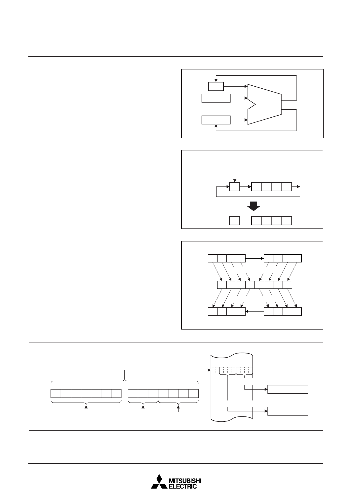
(9) Data pointer (DP)
Data pointer (DP) is used to specify a RAM address and consists
of registers Z, X, and Y. Register Z specifies a RAM file group, register X specifies a file, and register Y specifies a RAM digit (Figure
8).
Register Y is also used to specify the port D bit position.
When using port D, set the port D bit position to register Y certainly
and execute the SD, RD, or SZD instruction (Figure 9).
Program counter
p5p4p3p2p1p0a6a5a4a3a2a1a
p
6
PC
H
Specifying page
Fig. 7 Program counter (PC) structure
Specifying address
Data pointer (DP)
Z1Z0X3X2X1X0Y3Y2Y1Y
Register Y (4)
Register X (4)
Register Z (2)
Specifying RAM file group
0
PC
L
0
Specifying
RAM digit
Specifying RAM file
Fig. 8 Data pointer (DP) structure
Specifying bit position
D
7
0101 1
Register Y (4)
Fig. 9 SD instruction execution example
Port D output latch
Set
D
5
D
6
D4D
0
17
Y
PRELIMINAR
Notice: This is not a final specification.
Some parametric limits are subject to
change.
MITSUBISHI MICROCOMPUTERS
4513/4514 Group
SINGLE-CHIP 4-BIT CMOS MICROCOMPUTER
PROGRAM MEMORY (ROM)
The program memory is a mask ROM. 1 word of ROM is composed
of 10 bits. ROM is separated every 128 words by the unit of page
(addresses 0 to 127). Table 1 shows the ROM size and pages. Figure 10 shows the ROM map of M34514M8/E8.
Table 1 ROM size and pages
Product
M34513M2
M34513M4/E4
M34513M6
M34513M8/E8
M34514M6
M34514M8/E8
A part of page 1 (addresses 008016 to 00FF16) is reserved for interrupt addresses (Figure 11). When an interrupt occurs, the
address (interrupt address) corresponding to each interrupt is set
in the program counter, and the instruction at the interrupt address
is executed. When using an interrupt service routine, write the instruction generating the branch to that routine at an interrupt
address.
Page 2 (addresses 0100
routine calls. Subroutines written in this page can be called from
any page with the 1-word instruction (BM). Subroutines extending
from page 2 to another page can also be called with the BM instruction when it starts on page 2.
ROM pattern (bits 7 to 0) of all addresses can be used as data areas with the TABP p instruction.
ROM size
(✕ 10 bits)
2048 words
4096 words
6144 words
8192 words
6144 words
8192 words
16 to 017F16) is the special page for sub-
Pages
16 (0 to 15)
32 (0 to 31)
48 (0 to 47)
64 (0 to 63)
48 (0 to 47)
64 (0 to 63)
9
16
0000
007
F
16
0080
16
00
FF
0100
017
0180
0
FFF
1
FFF
F
Interrupt address page
16
16
Subroutine special page
16
16
16
16
Fig. 10 ROM map of M34514M8/E8
9087654321
0080
0082
0084
0086
0088
External 0 interrupt address
16
External 1 interrupt address
16
Timer 1 interrupt address
16
16
Timer 2 interrupt address
Timer 3 interrupt address
16
087654321
Page 0
Page 1
Page 2
Page 3
Page 31
Page 63
008A
16
Timer 4 interrupt address
16
008C
008E
16
00FF
16
Fig. 11 Page 1 (addresses 008016 to 00FF16) structure
A-D interrupt address
Serial I/O interrupt address
18
PRELIMINARY
Notice: This is not a final specification.
Some parametric limits are subject to
change.
MITSUBISHI MICROCOMPUTERS
4513/4514 Group
SINGLE-CHIP 4-BIT CMOS MICROCOMPUTER
DATA MEMORY (RAM)
1 word of RAM is composed of 4 bits, but 1-bit manipulation (with
the SB j, RB j, and SZB j instructions) is enabled for the entire
memory area. A RAM address is specified by a data pointer. The
data pointer consists of registers Z, X, and Y. Set a value to the
data pointer certainly when executing an instruction to access
RAM.
Table 2 shows the RAM size. Figure 12 shows the RAM map.
RAM 384 words ✕ 4 bits (1536 bits)
Register Z
01 7
23 6 015
M34513M6
M34513M8/E8
M34514M6
M34514M8/E8
M34513M4/E4
Register X
Register Y
10
11
12
13
14
15
Z=0, X=0 to 15
Z=1, X=0 to 7
Z=0, X=0 to 15
0
1
2
3
4
5
6
7
8
9
Table 2 RAM size
M34513M2
M34513M4/E4
M34513M6
M34513M8/E8
M34514M6
M34514M8/E8
0
45
Product
128 words ✕ 4 bits (512 bits)
256 words ✕ 4 bits (1024 bits)
384 words ✕ 4 bits (1536 bits)
384 words ✕ 4 bits (1536 bits)
384 words ✕ 4 bits (1536 bits)
384 words ✕ 4 bits (1536 bits)
1
1723 6
256 words
45
384 words
RAM size
Fig. 12 RAM map
M34513M2
Z=0, X=0 to 7
128 words
19
PRELIMINARY
Notice: This is not a final specification.
Some parametric limits are subject to
change.
MITSUBISHI MICROCOMPUTERS
4513/4514 Group
SINGLE-CHIP 4-BIT CMOS MICROCOMPUTER
INTERRUPT FUNCTION
The interrupt type is a vectored interrupt branching to an individual
address (interrupt address) according to each interrupt source. An
interrupt occurs when the following 3 conditions are satisfied.
• An interrupt activated condition is satisfied (request flag = “1”)
• Interrupt enable bit is enabled (“1”)
• Interrupt enable flag is enabled (INTE = “1”)
Table 3 shows interrupt sources. (Refer to each interrupt request
flag for details of activated conditions.)
(1) Interrupt enable flag (INTE)
The interrupt enable flag (INTE) controls whether the every interrupt enable/disable. Interrupts are enabled when INTE flag is set to
“1” with the EI instruction and disabled when INTE flag is cleared to
“0” with the DI instruction. When any interrupt occurs, the INTE flag
is automatically cleared to “0,” so that other interrupts are disabled
until the EI instruction is executed.
(2) Interrupt enable bit
Use an interrupt enable bit of interrupt control registers V1 and V2
to select the corresponding interrupt or skip instruction.
Table 4 shows the interrupt request flag, interrupt enable bit and
skip instruction.
Table 5 shows the interrupt enable bit function.
(3) Interrupt request flag
When the activated condition for each interrupt is satisfied, the corresponding interrupt request flag is set to “1.” Each interrupt
request flag is cleared to “0” when either;
• an interrupt occurs, or
• the next instruction is skipped with a skip instruction.
Each interrupt request flag is set when the activated condition is
satisfied even if the interrupt is disabled by the INTE flag or its interrupt enable bit. Once set, the interrupt request flag retains set
until a clear condition is satisfied.
Accordingly, an interrupt occurs when the interrupt disable state is
released while the interrupt request flag is set.
If more than one interrupt request flag is set when the interrupt disable state is released, the interrupt priority level is as follows
shown in Table 3.
Table 3 Interrupt sources
Priority
level
1
2
3
4
5
6
7
8
Table 4 Interrupt request flag, interrupt enable bit and skip in-
Interrupt name
External 0 interrupt
External 1 interrupt
Timer 1 interrupt
Timer 2 interrupt
Timer 3 interrupt
Timer 4 interrupt
A-D interrupt
Serial I/O interrupt
Table 5 Interrupt enable bit function
Interrupt enable bit
Interrupt name
External 0 interrupt
External 1 interrupt
Timer 1 interrupt
Timer 2 interrupt
Timer 3 interrupt
Timer 4 interrupt
A-D interrupt
Serial I/O interrupt
struction
Request flag
Occurrence of interrupt
1
0
Activated condition
Level change of
INT0 pin
Level change of
INT1 pin
Timer 1 underflow
Timer 2 underflow
Timer 3 underflow
Timer 4 underflow
Completion of
A-D conversion
Completion of
serial I/O transfer
EXF0
EXF1
T1F
T2F
T3F
T4F
ADF
SIOF
Enabled
Disabled
Skip instruction
SNZ0
SNZ1
SNZT1
SNZT2
SNZT3
SNZT4
SNZAD
SNZSI
Interrupt
address
Address 0
in page 1
Address 2
in page 1
Address 4
in page 1
Address 6
in page 1
Address 8
in page 1
Address A
in page 1
Address C
in page 1
Address E
in page 1
Enable bit
V10
V11
V12
V13
V20
V21
V22
V23
Skip instruction
Invalid
Valid
20
PRELIMINARY
Notice: This is not a final specification.
Some parametric limits are subject to
change.
MITSUBISHI MICROCOMPUTERS
4513/4514 Group
SINGLE-CHIP 4-BIT CMOS MICROCOMPUTER
(4) Internal state during an interrupt
The internal state of the microcomputer during an interrupt is as follows (Figure 14).
• Program counter (PC)
An interrupt address is set in program counter. The address to be
executed when returning to the main routine is automatically
stored in the stack register (SK).
• Interrupt enable flag (INTE)
INTE flag is cleared to “0” so that interrupts are disabled.
• Interrupt request flag
Only the request flag for the current interrupt source is cleared to
“0.”
• Data pointer, carry flag, skip flag, registers A and B
The contents of these registers and flags are stored automatically
in the interrupt stack register (SDP).
(5) Interrupt processing
When an interrupt occurs, a program at an interrupt address is executed after branching a data store sequence to stack register.
Write the branch instruction to an interrupt service routine at an interrupt address.
Use the RTI instruction to return from an interrupt service routine.
Interrupt enabled by executing the EI instruction is performed after
executing 1 instruction (just after the next instruction is executed).
Accordingly, when the EI instruction is executed just before the RTI
instruction, interrupts are enabled after returning the main routine.
(Refer to Figure 13)
• Program counter (PC)
.............................................................. Each interrupt address
• Stack register (SK)
....................................................................................................
The address of main routine to be
executed when returning
• Interrupt enable flag (INTE)
.................................................................. 0 (Interrupt disabled)
• Interrupt request flag (only the flag for the current interrupt
source)................................................................................... 0
• Data pointer, carry flag, registers A and B, skip flag
........ Stored in the interrupt stack register (SDP) automatically
Fig. 14 Internal state when interrupt occurs
INT0 pin
(L→H or
H→L input)
INT1 pin
(L→H or
H→L input)
Timer 1
underflow
EXF0
EXF1 V1
T1F V1
V1
0
1
2
Address 0
in page 1
Address 2
in page 1
Address 4
in page 1
Main
rouine
Interrupt
service routine
Interrupt
occurs
•
•
•
•
EI
RTI
Interrupt is
enabled
: Interrupt enabled state
: Interrupt disabled state
Fig. 13 Program example of interrupt processing
Timer 2
underflow
Timer 3
underflow
Timer 4
underflow
Completion of
A-D conversion
Completion of
serial I/O transfer
Activated
condition
T2F V1
T3F V2
T4F V2
ADF V2
SIOF V2
Request flag
(state retained)
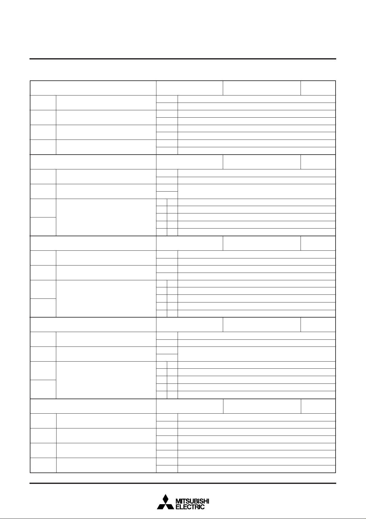
Fig. 15 Interrupt system diagram
3
0
1
2
3
Enable
bit
INTE
Enable
flag
Address 6
in page 1
Address 8
in page 1
Address A
in page 1
Address C
in page 1
Address E
in page 1
21
PRELIMINARY
Notice: This is not a final specification.
Some parametric limits are subject to
change.
MITSUBISHI MICROCOMPUTERS
4513/4514 Group
SINGLE-CHIP 4-BIT CMOS MICROCOMPUTER
(6) Interrupt control registers
• Interrupt control register V1
Interrupt enable bits of external 0, external 1, timer 1 and timer 2
are assigned to register V1. Set the contents of this register
through register A with the TV1A instruction. The TAV1 instruction
can be used to transfer the contents of register V1 to register A.
Table 6 Interrupt control registers
Interrupt control register V1
V13
V12
V11
V10
V23
V22
V21
V20
Note: “R” represents read enabled, and “W” represents write enabled.
Timer 2 interrupt enable bit
Timer 1 interrupt enable bit
External 1 interrupt enable bit
External 0 interrupt enable bit
Interrupt control register V2 R/Wat RAM back-up : 00002
Serial I/O interrupt enable bit
A-D interrupt enable bit
Timer 4 interrupt enable bit
Timer 3 interrupt enable bit
• Interrupt control register V2
Interrupt enable bits of timer 3, timer 4, A-D and serial I/O are assigned to register V2. Set the contents of this register through
register A with the TV2A instruction. The TAV2 instruction can be
used to transfer the contents of register V2 to register A.
at RAM back-up : 00002
at reset : 00002 R/W
at reset : 00002
0
Interrupt disabled (SNZT2 instruction is valid)
1
Interrupt enabled (SNZT2 instruction is invalid)
0
Interrupt disabled (SNZT1 instruction is valid)
1
Interrupt enabled (SNZT1 instruction is invalid)
0
Interrupt disabled (SNZ1 instruction is valid)
1
Interrupt enabled (SNZ1 instruction is invalid)
0
Interrupt disabled (SNZ0 instruction is valid)
1
Interrupt enabled (SNZ0 instruction is invalid)
at reset : 00002
0
Interrupt disabled (SNZSI instruction is valid)
1
Interrupt enabled (SNZSI instruction is invalid)
0
Interrupt disabled (SNZAD instruction is valid)
1
Interrupt enabled (SNZAD instruction is invalid)
0
Interrupt disabled (SNZT4 instruction is valid)
1
Interrupt enabled (SNZT4 instruction is invalid)
0
Interrupt disabled (SNZT3 instruction is valid)
1
Interrupt enabled (SNZT3 instruction is invalid)
at RAM back-up : 00002
R/W
22
PRELIMINARY
Notice: This is not a final specification.
Some parametric limits are subject to
change.
MITSUBISHI MICROCOMPUTERS
4513/4514 Group
SINGLE-CHIP 4-BIT CMOS MICROCOMPUTER
(7) Interrupt sequence
Interrupts only occur when the respective INTE flag, interrupt enable bits (V10–V13 and V20–V23), and interrupt request flag are
“1.” The interrupt actually occurs 2 to 3 machine cycles after the
cycle in which all three conditions are satisfied. The interrupt oc-
When an interrupt request flag is set after its interrupt is enabled (Note 1)
f (XIN) (middle-speed mode)
IN) (high-speed mode)
f (X
1 machine cycle
System clock
Interrupt enable
flag (INTE)
T2 T3
T1
EI instruction
execution cycle
T2 T3
T1
curs after 3 machine cycles only when the three interrupt conditions are satisfied on execution of other than one-cycle instructions
(Refer to Figure 16).
T2 T3
T1
Interrupt enabled state
T2 T3
T1
Interrupt disabled state
T2 T3
T1
INT0, INT1
External
interrupt
EXF0, EXF1
Timer 1,
Timer 2,
Timer 3,
Timer 4,
A-D, and
Serial I/O
interrupts
Notes 1: The 4513/4514 Group operates in the middle-speed mode after system is released from reset.
T1F, T2F, T3F,
T4F, ADF,SIOF
2: The address is stacked to the last cycle.
3: This interval of cycles depends on the executed instruction at the time when each interrupt activated condition is satisfied.
Fig. 16 Interrupt sequence
Interrupt activated
condition is satisfied.
2 to 3 machine cycles
(Notes 2, 3)
Retaining level of system
clock for 4 periods or more
is necessary.
Flag cleared
The program starts from
the interrupt address.
23
PRELIMINARY
Notice: This is not a final specification.
Some parametric limits are subject to
change.
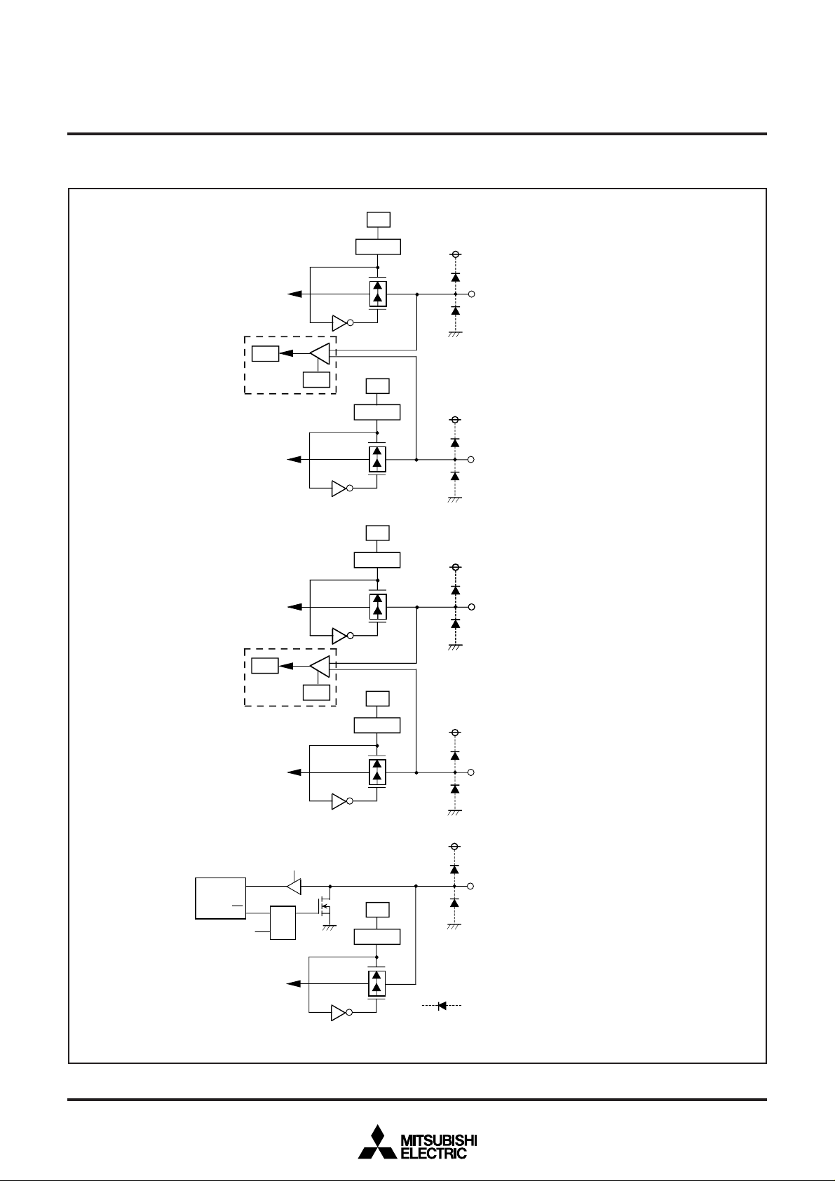
EXTERNAL INTERRUPTS
The 4513/4514 Group has two external interrupts (external 0 and
external 1). An external interrupt request occurs when a valid
waveform is input to an interrupt input pin (edge detection).
The external interrupts can be controlled with the interrupt control
registers I1 and I2.
Table 7 External interrupt activated conditions
Name
External 0 interrupt
External 1 interrupt
Input pin
P30/INT0
P31/INT1
When the next waveform is input to P30/INT0 pin
• Falling waveform (“H”→“L”)
• Rising waveform (“L”→“H”)
• Both rising and falling waveforms
When the next waveform is input to P31/INT1 pin
• Falling waveform (“H”→“L”)
• Rising waveform (“L”→“H”)
• Both rising and falling waveforms
SINGLE-CHIP 4-BIT CMOS MICROCOMPUTER
Activated condition
MITSUBISHI MICROCOMPUTERS
4513/4514 Group
Valid waveform
selection bit
I11
I12
I21
I22
I1
2
Falling
I2
Rising
2
Falling
Rising
0
1
0
1
SNZI1
P3
0
/INT0
P3
1
/INT1
SNZI0
One-sided edge
detection circuit
Both edges
detection circuit
Wakeup
One-sided edge
detection circuit
Both edges
detection circuit
Wakeup
Skip
Skip
I1
1
0
1
I2
1
0
1
EXF0
EXF1
External 0
interrupt
External 1
interrupt
Fig. 17 External interrupt circuit structure
24

PRELIMINARY
Notice: This is not a final specification.
Some parametric limits are subject to
change.
MITSUBISHI MICROCOMPUTERS
4513/4514 Group
SINGLE-CHIP 4-BIT CMOS MICROCOMPUTER
(1) External 0 interrupt request flag (EXF0)
External 0 interrupt request flag (EXF0) is set to “1” when a valid
waveform is input to P30/INT0 pin.
The valid waveforms causing the interrupt must be retained at their
level for 4 clock cycles or more of the system clock (Refer to Figure
16).
The state of EXF0 flag can be examined with the skip instruction
(SNZ0). Use the interrupt control register V1 to select the interrupt
or the skip instruction. The EXF0 flag is cleared to “0” when an interrupt occurs or when the next instruction is skipped with the skip
instruction.
The P30/INT0 pin need not be selected the external interrupt input
INT0 function or the normal I/O port P30 function. However, the
EXF0 flag is set to “1” when a valid waveform is input even if it is
used as an I/O port P30.
• External 0 interrupt activated condition
External 0 interrupt activated condition is satisfied when a valid
waveform is input to P30/INT0 pin.
The valid waveform can be selected from rising waveform, falling
waveform or both rising and falling waveforms. An example of
how to use the external 0 interrupt is as follows.
➀ Select the valid waveform with the bits 1 and 2 of register I1.
➁ Clear the EXF0 flag to “0” with the SNZ0 instruction.
➂ Set the NOP instruction for the case when a skip is performed
with the SNZ0 instruction.
➃ Set both the external 0 interrupt enable bit (V10) and the INTE
flag to “1.”
(2) External 1 interrupt request flag (EXF1)
External 1 interrupt request flag (EXF1) is set to “1” when a valid
waveform is input to P31/INT1 pin.
The valid waveforms causing the interrupt must be retained at their
level for 4 clock cycles or more of the system clock (Refer to Figure
16).
The state of EXF1 flag can be examined with the skip instruction
(SNZ1). Use the interrupt control register V1 to select the interrupt
or the skip instruction. The EXF1 flag is cleared to “0” when an interrupt occurs or when the next instruction is skipped with the skip
instruction.
The P31/INT1 pin need not be selected the external interrupt input
INT1 function or the normal I/O port P31 function. However, the
EXF1 flag is set to “1” when a valid waveform is input even if it is
used as an I/O port P31.
• External 1 interrupt activated condition
External 1 interrupt activated condition is satisfied when a valid
waveform is input to P31/INT1 pin.
The valid waveform can be selected from rising waveform, falling
waveform or both rising and falling waveforms. An example of
how to use the external 1 interrupt is as follows.
➀ Select the valid waveform with the bits 1 and 2 of register I2.
➁ Clear the EXF1 flag to “0” with the SNZ1 instruction.
➂ Set the NOP instruction for the case when a skip is performed
with the SNZ1 instruction.
➃ Set both the external 1 interrupt enable bit (V11) and the INTE
flag to “1.”
The external 0 interrupt is now enabled. Now when a valid waveform is input to the P30/INT0 pin, the EXF0 flag is set to “1” and the
external 0 interrupt occurs.
The external 1 interrupt is now enabled. Now when a valid waveform is input to the P31/INT1 pin, the EXF1 flag is set to “1” and the
external 1 interrupt occurs.
25
PRELIMINARY
Notice: This is not a final specification.
Some parametric limits are subject to
change.
MITSUBISHI MICROCOMPUTERS
4513/4514 Group
SINGLE-CHIP 4-BIT CMOS MICROCOMPUTER
(3) External interrupt control registers
• Interrupt control register I1
Register I1 controls the valid waveform for the external 0 interrupt. Set the contents of this register through register A with the
TI1A instruction. The TAI1 instruction can be used to transfer the
contents of register I1 to register A.
Table 8 External interrupt control registers
Interrupt control register I1 R/Wat RAM back-up : state retained
I13
I12
I11
I10
I23
I22
I21
I20
Notes 1: “R” represents read enabled, and “W” represents write enabled.
Not used
Interrupt valid waveform for INT0 pin/
return level selection bit (Note 2)
INT0 pin edge detection circuit control bit
INT0 pin
timer 1 control enable bit
Interrupt control register I2 R/Wat RAM back-up : state retainedat reset : 00002
Not used
Interrupt valid waveform for INT1 pin/
return level selection bit (Note 3)
INT1 pin edge detection circuit control bit
INT1 pin
timer 3 control enable bit
2: When the contents of I1
3: When the contents of I2
2 is changed, the external interrupt request flag EXF0 may be set. Accordingly, clear EXF0 flag with the SNZ0 instruction.
2 is changed, the external interrupt request flag EXF1 may be set. Accordingly, clear EXF1 flag with the SNZ1 instruction.
0
1
0
1
0
1
0
1
0
1
0
1
0
1
0
1
• Interrupt control register I2
Register I2 controls the valid waveform for the external 1 interrupt. Set the contents of this register through register A with the
TI2A instruction. The TAI2 instruction can be used to transfer the
contents of register I2 to register A.
at reset : 00002
This bit has no function, but read/write is enabled.
Falling waveform (“L” level of INT0 pin is recognized with the SNZI0
instruction)/“L” level
Rising waveform (“H” level of INT0 pin is recognized with the SNZI0
instruction)/“H” level
One-sided edge detected
Both edges detected
Disabled
Enabled
This bit has no function, but read/write is enabled.
Falling waveform (“L” level of INT1 pin is recognized with the SNZI1
instruction)/“L” level
Rising waveform (“H” level of INT1 pin is recognized with the SNZI1
instruction)/“H” level
One-sided edge detected
Both edges detected
Disabled
Enabled
26
PRELIMINARY
Notice: This is not a final specification.
Some parametric limits are subject to
change.
MITSUBISHI MICROCOMPUTERS
4513/4514 Group
SINGLE-CHIP 4-BIT CMOS MICROCOMPUTER
TIMERS
The 4513/4514 Group has the programmable timers.
• Programmable timer
The programmable timer has a reload register and enables the
frequency dividing ratio to be set. It is decremented from a setting
value n. When it underflows (count to n + 1), a timer interrupt request flag is set to “1,” new data is loaded from the reload
register, and count continues (auto-reload function).
FF
16
n : Counter initial value
Count starts
n
1st underflow 2nd underflow
The contents of counter
16
00
n+1 count n+1 count
• Fixed dividing frequency timer
The fixed dividing frequency timer has the fixed frequency dividing ratio (n). An interrupt request flag is set to “1” after every n
count of a count pulse.
Reload Reload
Time
Timer interrupt
request flag
Fig. 18 Auto-reload function
“1”
“0”
An interrupt occurs or
a skip instruction is executed.
27
PRELIMINARY
Notice: This is not a final specification.
Some parametric limits are subject to
change.
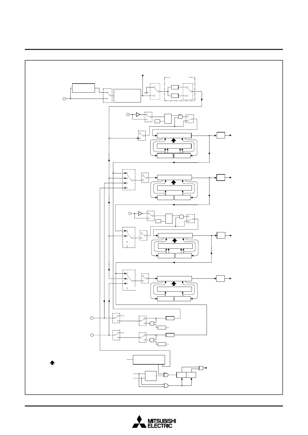
The 4513/4514 Group timer consists of the following circuits.
• Prescaler : frequency divider
• Timer 1 : 8-bit programmable timer
• Timer 2 : 8-bit programmable timer
• Timer 3 : 8-bit programmable timer
• Timer 4 : 8-bit programmable timer
(Timers 1 to 4 have the interrupt function, respectively)
• 16-bit timer
Prescaler and timers 1 to 4 can be controlled with the timer control
registers W1 to W6. The 16-bit timer is a free counter which is not
controlled with the control register.
Each function is described below.
Table 9 Function related timers
Circuit
Prescaler
Timer 1
Timer 2
Timer 3
Timer 4
16-bit timer
Structure
Frequency divider
8-bit programmable
binary down counter
(link to EXF0)
8-bit programmable
binary down counter
8-bit programmable
binary down counter
(link to EXF1)
8-bit programmable
binary down counter
16-bit fixed dividing
frequency
Count source
• Instruction clock
• Prescaler output (ORCLK)
• Timer 1 underflow
• Prescaler output (ORCLK)
• CNTR0 input
• 16-bit counter underflow
• Timer 2 underflow
• Prescaler output (ORCLK)
• Timer 3 underflow
• Prescaler output (ORCLK)
• CNTR1 input
• Instruction clock
Frequency
dividing ratio
4, 16
1 to 256
1 to 256
1 to 256
1 to 256
65536
MITSUBISHI MICROCOMPUTERS
4513/4514 Group
SINGLE-CHIP 4-BIT CMOS MICROCOMPUTER
Use of output signal
• Timer 1, 2, 3 and 4 count sources
• Timer 2 count source
• CNTR0 output
• Timer 1 interrupt
• Timer 3 count source
• Timer 2 interrupt
• CNTR0 output
• Timer 4 count source
• Timer 3 interrupt
• CNTR1 output
• Timer 4 interrupt
• CNTR1 output
• Watchdog timer
(The 15th bit is counted twice)
• Timer 2 count source
(16-bit counter underflow)
Control
register
W1
W1
W6
W2
W6
W3
W6
W4
W6
28
PRELIMINARY
Notice: This is not a final specification.
Some parametric limits are subject to
change.
Division circuit
(divided by 2)
X
IN
MR
3
1
Internal clock
generation circuit
0
(divided by 3)
P30/INT0
Instruction clock
W1
I1
2
0
1
(Note)W1
1
0
1
(TAB1)
SINGLE-CHIP 4-BIT CMOS MICROCOMPUTER
Prescaler
3
0
1
I1
T1AB
1/4
1/16
ORCLK
Q
S
0
R
Timer 1 (8)
Reload register R1 (8)
(TR1AB)
Register B
Register A
W1
W1
T1AB
MITSUBISHI MICROCOMPUTERS
4513/4514 Group
2
0
1
0
1
0
Timer 1
T1F
interrupt
D6/CNTR0
D7/CNTR1
P31/INT1
W6
0
0
1
W6
2
0
1
W21,W2
00
01
10
11
W31,W3
00
01
10
Not available
11
Not available
W41,W4
00
01
10
11
Not available
D
6
output
7
output
D
0
W23(Note)
(TAB2)
0
W33(Note)
(TAB3)
0
W43(Note)
(TAB4)
W6
0
1
W6
0
1
Timer 1 underflow signal
0
1
Reload register R2 (8)
Register B
Timer 2 underflow signal
I2
2
0
1
I2
0
0
1
Reload register R3 (8)
T3AB
Register B
Timer 3 underflow signal
0
1
Reload register R4 (8)
Register B
1
3
1/2
1/2
Timer 2 (8)
(T2AB)
Register A
Q
S
R
W3
1
0
Timer 3 (8)
(TR3AB)
T3AB
Register A
Timer 4 (8)
(T4AB)
Register A
1/2
Timer 2 underflow signal
1/2
Timer 4 underflow signal
Timer 2
T2F
interrupt
2
T3F
Timer 3
interrupt
Timer 4
T4F
interrupt
Data is set automatically from
each reload register when timer
1, 2, 3, or 4 underflows (autoreload function)
Note: Count source is stopped by
clearing to “0.”
Fig. 19 Timers structure
Instruction clock
WRST instruction
Reset signal
16-bit timer (WDT)
1 - - - - - - - - - - - 15 16
S
WEF
Q
R
System reset
WDF1 WDF2
29
PRELIMINARY
Notice: This is not a final specification.
Some parametric limits are subject to
change.
Table 10 Timer control registers
MITSUBISHI MICROCOMPUTERS
4513/4514 Group
SINGLE-CHIP 4-BIT CMOS MICROCOMPUTER
W13
W12
W11
W10
W23
W22
W21
W20
W33
W32
W31
W30
Timer control register W1 R/Wat RAM back-up : 00002
Prescaler control bit
Prescaler dividing ratio selection bit
Timer 1 control bit
Timer 1 count start synchronous circuit
control bit
Timer control register W2 R/Wat RAM back-up : state retainedat reset : 00002
Timer 2 control bit
Not used
Timer 2 count source selection bits
Timer control register W3
Timer 3 control bit
Timer 3 count start synchronous circuit
control bit
Timer 3 count source selection bits
W21
0
0
1
1
W31
0
0
1
1
0
1
0
1
0
1
0
1
0
1
0
1
W20
0
1
0
1
0
1
0
1
W30
0
1
0
1
at reset : 00002
at reset : 00002
Stop (state initialized)
Operating
Instruction clock divided by 4
Instruction clock divided by 16
Stop (state retained)
Operating
Count start synchronous circuit not selected
Count start synchronous circuit selected
Stop (state retained)
Operating
This bit has no function, but read/write is enabled.
Count source
Timer 1 underflow signal
Prescaler output
CNTR0 input
16 bit timer (WDT) underflow signal
at reset : 00002
Stop (state retained)
Operating
Count start synchronous circuit not selected
Count start synchronous circuit selected
Timer 2 underflow signal
Prescaler output
Not available
Not available
at RAM back-up : state retained
Count source
R/Wat RAM back-up : 00002
R/W
Timer control register W4
W43
W42
W41
W40
W63
W62
W61
W60
Note: “R” represents read enabled, and “W” represents write enabled.
30
Timer 4 control bit
Not used
W41
0
Timer 4 count source selection bits
Timer control register W6 R/Wat RAM back-up : state retainedat reset : 00002
CNTR1 output control bit
D7/CNTR1 function selection bit
CNTR0 output control bit
D6/CNTR0 output control bit
0
1
1
at reset : 00002
Stop (state retained)
0
Operating
1
0
This bit has no function, but read/write is enabled.
1
W40
Timer 3 underflow signal
0
Prescaler output
1
CNTR1 input
0
Not available
1
Timer 3 underflow signal output divided by 2
0
CNTR1 output control by timer 4 underflow signal divided by 2
1
D7(I/O)/CNTR1 input
0
CNTR1 (I/O)/D7(input)
1
Timer 1 underflow signal output divided by 2
0
CNTR0 output control by timer 2 underflow signal divided by 2
1
D6(I/O)/CNTR0 input
0
CNTR0 (I/O)/D6(input)
1
at RAM back-up : state retained
Count source
R/W

PRELIMINARY
Notice: This is not a final specification.
Some parametric limits are subject to
change.
MITSUBISHI MICROCOMPUTERS
4513/4514 Group
SINGLE-CHIP 4-BIT CMOS MICROCOMPUTER
(1) Timer control registers
• Timer control register W1
Register W1 controls the count operation of timer 1, the selection
of count start synchronous circuit, and the frequency dividing ratio and count operation of prescaler. Set the contents of this
register through register A with the TW1A instruction. The TAW1
instruction can be used to transfer the contents of register W1 to
register A.
• Timer control register W2
Register W2 controls the count operation and count source of
timer 2. Set the contents of this register through register A with
the TW2A instruction. The TAW2 instruction can be used to transfer the contents of register W2 to register A.
• Timer control register W3
Register W3 controls the count operation and count source of
timer 3 and the selection of count start synchronous circuit. Set
the contents of this register through register A with the TW3A instruction. The TAW3 instruction can be used to transfer the
contents of register W3 to register A.
• Timer control register W4
Register W4 controls the count operation and count source of
timer 4. Set the contents of this register through register A with
the TW4A instruction. The TAW4 instruction can be used to transfer the contents of register W4 to register A.
• Timer control register W6
Register W6 controls the D6/CNTR0 pin and D7/CNTR1 functions, the selection and operation of the CNTR0 and CNTR1
output. Set the contents of this register through register A with
the TW6A instruction. The TAW6 instruction can be used to transfer the contents of register W6 to register A.
(2) Precautions
Note the following for the use of timers.
• Prescaler
Stop the prescaler operation to change its frequency dividing ratio.
• Count source
Stop timer 1, 2, 3, or 4 counting to change its count source.
• Reading the count value
Stop timer 1, 2, 3, or 4 counting and then execute the TAB1,
TAB2, TAB3, or TAB4 instruction to read its data.
• Writing to reload registers R1 and R3
When writing data to reload registers R1 or R3 while timer 1 or
timer 3 is operating, avoid a timing when timer 1 or timer 3
underflows.
(3) Prescaler
Prescaler is a frequency divider. Its frequency dividing ratio can be
selected. The count source of prescaler is the instruction clock.
Use the bit 2 of register W1 to select the prescaler dividing ratio
and the bit 3 to start and stop its operation. Prescaler is initialized,
and the output signal (ORCLK) stops when the bit 3 of register W1
is cleared to “0.”
(4) Timer 1 (interrupt function)
Timer 1 is an 8-bit binary down counter with the timer 1 reload register (R1). Data can be set simultaneously in timer 1 and the reload
register (R1) with the T1AB instruction. Data can be written to reload register (R1) with the TR1AB instruction.
When writing data to reload register R1 with the TR1AB instruction,
the downcount after the underflow is started from the setting value
of reload register R1.
Timer 1 starts counting after the following process;
➀ set data in timer 1, and
➁ set the bit 1 of register W1 to “1.”
However, P30/INT0 pin input can be used as the start trigger for
timer 1 count operation by setting the bit 0 of register W1 to “1.”
Once count is started, when timer 1 underflows (the next count
pulse is input after the contents of timer 1 becomes “0”), the timer
1 interrupt request flag (T1F) is set to “1,” new data is loaded from
reload register R1, and count continues (auto-reload function).
When a value set in reload register R1 is n, timer 1 divides the
count source signal by n + 1 (n = 0 to 255).
Data can be read from timer 1 with the TAB1 instruction. When
reading the data, stop the counter and then execute the TAB1 instruction. Timer 1 underflow signal divided by 2 can be output from
D6/CNTR0 pin.
(5) Timer 2 (interrupt function)
Timer 2 is an 8-bit binary down counter with the timer 2 reload register (R2). Data can be set simultaneously in timer 2 and the reload
register (R2) with the T2AB instruction.
Timer 2 starts counting after the following process;
➀ set data in timer 2,
➁ select the count source with the bits 0 and 1 of register W2, and
➂ set the bit 3 of register W2 to “1.”
Once count is started, when timer 2 underflows (the next count
pulse is input after the contents of timer 2 becomes “0”), the timer
2 interrupt request flag (T2F) is set to “1,” new data is loaded from
reload register R2, and count continues (auto-reload function).
When a value set in reload register R2 is n, timer 2 divides the
count source signal by n + 1 (n = 0 to 255).
Data can be read from timer 2 with the TAB2 instruction. When
reading the data, stop the counter and then execute the TAB2 instruction. The output from D6/CNTR0 pin by timer 2 underflow
signal divided by 2 can be controlled.
31

PRELIMINARY
Notice: This is not a final specification.
Some parametric limits are subject to
change.
MITSUBISHI MICROCOMPUTERS
4513/4514 Group
SINGLE-CHIP 4-BIT CMOS MICROCOMPUTER
(6) Timer 3 (interrupt function)
Timer 3 is an 8-bit binary down counter with the timer 3 reload register (R3). Data can be set simultaneously in timer 3 and the reload
register (R3) with the T3AB instruction. Data can be written to reload register (R3) with the TR3AB instruction.
When writing data to reload register R3 with the TR3AB instruction,
the downcount after the underflow is started from the setting value
of reload register R3.
Timer 3 starts counting after the following process;
➀ set data in timer 3,
➁ select the count source with the bits 0 and 1 of register W3, and
➂ set the bit 3 of register W3 to “1.”
However, P31/INT1 pin input can be used as the start trigger for
timer 3 count operation by setting the bit 2 of register W3 to “1.”
Once count is started, when timer 3 underflows (the next count
pulse is input after the contents of timer 3 becomes “0”), the timer
3 interrupt request flag (T3F) is set to “1,” new data is loaded from
reload register R3, and count continues (auto-reload function).
When a value set in reload register R3 is n, timer 3 divides the
count source signal by n + 1 (n = 0 to 255).
Data can be read from timer 3 with the TAB3 instruction. When
reading the data, stop the counter and then execute the TAB3 instruction. Timer 3 underflow signal divided by 2 can be output from
D7/CNTR1 pin.
(7) Timer 4 (interrupt function)
Timer 4 is an 8-bit binary down counter with the timer 4 reload register (R4). Data can be set simultaneously in timer 4 and the reload
register (R4) with the T4AB instruction.
Timer 4 starts counting after the following process;
➀ set data in timer 4,
➁ select the count source with the bits 0 and 1 of register W4, and
➂ set the bit 3 of register W4 to “1.”
Once count is started, when timer 4 underflows (the next count
pulse is input after the contents of timer 4 becomes “0”), the timer
4 interrupt request flag (T4F) is set to “1,” new data is loaded from
reload register R4, and count continues (auto-reload function).
When a value set in reload register R4 is n, timer 4 divides the
count source signal by n + 1 (n = 0 to 255).
Data can be read from timer 4 with the TAB4 instruction. When
reading the data, stop the counter and then execute the TAB4 instruction. The output from D7/CNTR1 pin by timer 4 underflow
signal divided by 2 can be controlled.
(8) Timer I/O pin (D6/CNTR0, D7/CNTR1)
D6/CNTR0 pin has functions to input the timer 2 count source, and
to output the timer 1 and timer 2 underflow signals divided by 2.
D7/CNTR1 pin has functions to input the timer 4 count source, and
to output the timer 3 and timer 4 underflow signals divided by 2.
The selection of D6/CNTR0 pin function can be controlled with the
bit 0 of register W6. The selection of D7/CNTR1 pin function can be
controlled with the bit 2 of register W6.
The following signals can be selected for the CNTR0 output signal
with the bit 1 of register W6.
• timer 1 underflow signal divided by 2
• the signal of AND operation between timer 1 underflow signal divided by 2 and timer 2 underflow signal divide by 2
The following signals can be selected for the CNTR1 output signal
with the bit 3 of register W6.
• timer 3 underflow signal divided by 2
• the signal of AND operation between timer 3 underflow signal divided by 2 and timer 4 underflow signal divide by 2
Timer 2 counts the rising waveform of CNTR0 input when the
CNTR0 input is selected as the count source.
Timer 4 counts the rising waveform of CNTR1 input when the
CNTR1 input is selected as the count source.
(9) Timer interrupt request flags (T1F, T2F,
T3F, and T4F)
Each timer interrupt request flag is set to “1” when each timer
underflows. The state of these flags can be examined with the skip
instructions (SNZT1, SNZT2, SNZT3, and SNZT4).
Use the interrupt control registers V1, V2 to select an interrupt or a
skip instruction.
An interrupt request flag is cleared to “0” when an interrupt occurs
or when the next instruction is skipped with a skip instruction.
(10) Count start synchronization circuit (timer
1, timer 3)
Each timer 1 and timer 3 has the count start synchronization circuit
which synchronize P30/INT0 pin and P31/INT1 pin, respectively,
and can start the timer count operation.
Timer 1 count start synchronization circuit function is selected by
setting the bit 0 of register W1 to “1.” The control by P30/INT0 pin
input can be performed by setting the bit 0 of register I1 to “1.”
P30/INT0 pin input level can be selected by the bit 2 of register I1
as follows;
• I12 = “0”: The count start synchronizes the “L” level of P30/INT0 pin
• I12 = “1”: The count start synchronizes the “H” level of P30/INT0 pin
Timer 3 count start synchronization circuit function is selected by
setting the bit 2 of register W3 to “1.” The control by P31/INT1 pin
input can be performed by setting the bit 0 of register I2 to “1.”
P31/INT1 pin input level can be selected by the bit 2 of register I2
as follows;
• I22 = “0”: The count start synchronizes the “L” level of P31/INT1 pin
• I22 = “1”: The count start synchronizes the “H” level of P31/INT1 pin
When timer 1 and timer 3 count start synchronization circuits are
used, the count start synchronization circuits are set, the count
source is input to each timer by inputting valid levels to P30/INT0
pin and P31/INT1 pin. Once set, the count start synchronization circuit is cleared by clearing the bit I10 or I20 to “0” or reset.
32

PRELIMINARY
Notice: This is not a final specification.
Some parametric limits are subject to
change.
MITSUBISHI MICROCOMPUTERS
4513/4514 Group
SINGLE-CHIP 4-BIT CMOS MICROCOMPUTER
WATCHDOG TIMER
Watchdog timer provides a method to reset the system when a program runs wild. Watchdog timer consists of a 16-bit timer (WDT),
watchdog timer enable flag (WEF), and watchdog timer flags
(WDF1, WDF2).
The timer WDT downcounts the instruction clocks as the count
source. The underflow signal is generated when the count value
reaches “000016.” This underflow signal can be used as the timer 2
count source.
When the WRST instruction is executed after system is released
from reset, the WEF flag is set to “1”. At this time, the watchdog
timer starts operating.
FFFF
16
The value of timer (WDT)
0000
16
WEF flag
WDF1 flag
WDF2 flag
When the count value of timer WDT reaches “BFFF16” or “3FFF16,”
the WDF1 flag is set to “1.” If the WRST instruction is never executed while timer WDT counts 32767, WDF2 flag is set to “1,” and
the RESET pin outputs “L” level to reset the microcomputer. Execute the WRST instruction at each period of 32766 machine cycle
or less by software when using watchdog timer to keep the microcomputer operating normally.
To prevent the WDT stopping in the event of misoperation, WEF
flag is designed not to initialize once the WRST instruction has
been executed. Note also that, if the WRST instruction is never executed, the watchdog timer does not start.
BFFF
16
3FFF
16
RESET pin output
Fig. 20 Watchdog timer function
The contents of WEF, WDF1 and WDF2 flags and timer WDT are
initialized at the RAM back-up mode.
If WDF2 flag is set to “1” at the same time that the microcomputer
enters the RAM back-up state, system reset may be performed.
When using the watchdog timer and the RAM back-up mode, initialize the WDF1 flag with the WRST instruction just before the
microcomputer enters the RAM back-up state (refer to Figure 21)
WRST
instruction
executed
WRST
instruction
executed
•
•
•
•
•
•
System reset
WRST ; WDF1 flag reset
EPOF ; POF instruction enabled
POF
Oscillation
(RAM back-up state)
stop
Fig. 21 Program example to enter the RAM back-up mode
when using the watchdog timer
33

PRELIMINARY
Notice: This is not a final specification.
Some parametric limits are subject to
change.
MITSUBISHI MICROCOMPUTERS
4513/4514 Group
SINGLE-CHIP 4-BIT CMOS MICROCOMPUTER
SERIAL I/O
The 4513/4514 Group has a built-in clock synchronous serial I/O
which can serially transmit or receive 8-bit data.
Serial I/O consists of;
• serial I/O register SI
• serial I/O mode register J1
• serial I/O transmission/reception completion flag (SIOF)
• serial I/O counter
Registers A and B are used to perform data transfer with internal
CPU, and the serial I/O pins are used for external data transfer.
The pin functions of the serial I/O pins can be set with the register
J1.
MR
1/4
1/8
3
Internal clock
1
generation circuit
0
(divided by 3)
J1
2
1
0
Division circuit
(divided by 2)
X
IN
Table 11 Serial I/O pins
Pin
P20/SCK
P21/SOUT
P22/SIN
Note: Input ports P20–P22 can be used regardless of register J1.
Instruction clock
Serial I/O mode register J1
J1
3
Pin function when selecting serial I/O
Clock I/O (SCK)
Serial data output (SOUT)
Serial data input (SIN)
J12J11J1
0
S
P20/S
P21/S
P22/S
CK
OUT
IN
CK
S
OUT
S
IN
J1
1
Note: The output structure of S
MSB
J1
0
Fig. 22 Serial I/O structure
Table 12 Serial I/O mode register
Serial I/O mode register J1
J13
J12
J11
J10
Note: “R” represents read enabled, and “W” represents write enabled.
Not used
Serial I/O internal clock dividing ratio
selection bit
Serial I/O port selection bit
Serial I/O synchronous clock selection bit
Synchronous
circuit
Serial I/O register SI (8)
TSIAB TABSI
Register B (4)
CK
and S
OUT
at reset : 00002
0
This bit has no function, but read/write is enabled.
1
0
Instruction clock signal divided by 8
1
Instruction clock signal divided by 4
0
Input ports P20, P21, P22 selected
1
Serial I/O ports SCK, SOUT, SIN/input ports P20, P21, P22 selected
0
External clock
1
Internal clock (instruction clock divided by 4 or 8)
Serial I/O counter (3)
LSB
Register A (4)
pins is N-channel open-drain.
at RAM back-up : state retained
SIOF
Serial I/O interrupt
R/W
34

PRELIMINARY
Notice: This is not a final specification.
Some parametric limits are subject to
change.
When transmitting (D7–D0 : transfer data) When receiving
SIN pin
S
OUT
MITSUBISHI MICROCOMPUTERS
4513/4514 Group
SINGLE-CHIP 4-BIT CMOS MICROCOMPUTER
pin
S
OUT
pin
D7D6D5D4D3D2D1D
D7D6D5D4D3D2D1D
D7D6D5D4D3D2D
∗
∗∗
D7D6D5D4D3D
∗∗∗∗∗∗∗∗
Fig. 23 Serial I/O register state when transferring
0
0
Transfer data to be set
1
2
Transfer started
Transfer completed
(1) Serial I/O register SI
Serial I/O register SI is the 8-bit data transfer serial/parallel conversion register. Data can be set to register SI through registers A and
B with the TSIAB instruction. The contents of register A is transmitted to the low-order 4 bits of register SI, and the contents of
register B is transmitted to the high-order 4 bits of register SI.
During transmission, each bit data is transmitted LSB first from the
lowermost bit (bit 0) of register SI, and during reception, each bit
data is received LSB first to register SI starting from the topmost bit
(bit 7).
When register SI is used as a work register without using serial I/O,
pull up the SCK pin or set the pin function to an input port P20.
S
IN
pin
Serial I/O register (SI)Serial I/O register (SI)
∗
∗∗∗∗∗∗∗
∗∗∗∗∗∗∗∗
D
0
∗∗∗∗∗∗∗
D1D
D7D6D5D4D3D2D1D
(3) Serial I/O start instruction (SST)
When the SST instruction is executed, the SIOF flag is cleared to
“0” and then serial I/O transmission/reception is started.
(4) Serial I/O mode register J1
Register J1 controls the synchronous clock, P20/SCK, P21/SOUT
and P22/SIN pin function. Set the contents of this register through
register A with the TJ1A instruction. The TAJ1 instruction can be
used to transfer the contents of register J1 to register A.
∗∗∗∗∗∗
0
0
(2) Serial I/O transmission/reception
completion flag (SIOF)
Serial I/O transmission/reception completion flag (SIOF) is set to
“1” when serial data transmission or reception completes. The
state of SIOF flag can be examined with the skip instruction
(SNZSI). Use the interrupt control register V2 to select the interrupt or the skip instruction.
The SIOF flag is cleared to “0” when the interrupt occurs or when
the next instruction is skipped with the skip instruction.
35

PRELIMINARY
Notice: This is not a final specification.
Some parametric limits are subject to
change.
MITSUBISHI MICROCOMPUTERS
4513/4514 Group
SINGLE-CHIP 4-BIT CMOS MICROCOMPUTER
(5) How to use serial I/O
Figure 24 shows the serial I/O connection example. Serial I/O interrupt is not used in this example. In the actual wiring, pull up the
Master (clock control)
D5
SCK
SOUT
SIN
1
(Bit 0)
1
Serial I/O mode register J1
Internal clock selected as
a synchronous clock
(Bit 3)
✕✕
wiring between each pin with a resistor. Figure 25 shows the data
transfer timing and Table 13 shows the data transfer sequence.
Slave (external clock)
SRDY signal
D5
SCK
SIN
SOUT
(Bit 3)
✕✕
(Bit 0)
01
Serial I/O mode register J1
External clock selected as
a synchronous clock
Serial I/O port
CK,SOUT,SIN
S
Instruction clock divided by
8 or 4 selected as a transfer
clock
(Bit 3) (Bit 0) (Bit 3) (Bit 0)
0
✕✕✕
Interrupt control register V2
0
✕
Serial I/O interrupt enable bit
(SNZSI instruction is valid)
Fig. 24 Serial I/O connection example
✕✕
Serial I/O port
S
CK,SOUT,SIN
This bit is not valid
when J1
0=“0”
Interrupt control register V2
Serial I/O interrupt enable bit
(SNZSI instruction is valid)
✕ : Set an arbitrary value.
36

PRELIMINARY
Notice: This is not a final specification.
Some parametric limits are subject to
change.
Master
MITSUBISHI MICROCOMPUTERS
4513/4514 Group
SINGLE-CHIP 4-BIT CMOS MICROCOMPUTER
OUT
S
SIN
SST instruction
SCK
1M2
M0M7’
M
S0S7’S1S2S3S4S5S6S7
M3M4M5M6M7
Slave
SST instruction
S
RDY signal
SOUT
SIN
S7’
S0
S1S3S4S5S6S7
S2
M0M7’M1M2M3M4M5M6M7
M0–M7 : the contents of master serial I/O S0–S7 : the contents of slave serial I/O register
Rising of SCK : serial input Falling of SCK : serial output
Fig. 25 Timing of serial I/O data transfer
37

PRELIMINARY
Notice: This is not a final specification.
Some parametric limits are subject to
change.
Table 13 Processing sequence of data transfer from master to slave
Master (transmission)
[Initial setting]
• Setting the serial I/O mode register J1 and interrupt control register V2 shown in Figure 24.
TJ1A and TV2A instructions
• Setting the port received the reception enable
signal (SRDY) to the input mode.
(Port D5 is used in this example)
SD instruction
* [Transmission enable state]
• Storing transmission data to serial I/O register SI.
TSIAB instruction
[Transmission]
•Check port D5 is “L” level.
SZD instruction
•Serial transfer starts.
SST instruction
•Check transmission completes.
SNZSI instruction
•Wait (timing when continuously transferring)
[Initial setting]
• Setting serial I/O mode register J1, and interrupt control register V2 shown in
Figure 24.
• Setting the port received the reception enable signal (SRDY) and outputting “H”
level (reception impossible).
(Port D5 is used in this example)
*[Reception enable state]
• The SIOF flag is cleared to “0.”
• “L” level (reception possible) is output from port D5.
[Reception]
• Check reception completes.
• “H” level is output from port D5.
[Data processing]
MITSUBISHI MICROCOMPUTERS
4513/4514 Group
SINGLE-CHIP 4-BIT CMOS MICROCOMPUTER
Slave (reception)
TJ1A and TV2A instructions
SD instruction
SST instruction
RD instruction
SNZSI instruction
SD instruction
1-byte data is serially transferred on this process. Subsequently, data
can be transferred continuously by repeating the process from *.
When an external clock is selected as a synchronous clock, the
clock is not controlled internally. Control the clock externally because serial transfer is performed as long as clock is externally
input. (Unlike an internal clock, an external clock is not stopped
when serial transfer is completed.) However, the SIOF flag is set to
“1” when the clock is counted 8 times after executing the SST instruction. Be sure to set the initial level of the external clock to “H.”
38

PRELIMINARY
Notice: This is not a final specification.
Some parametric limits are subject to
change.
MITSUBISHI MICROCOMPUTERS
4513/4514 Group
SINGLE-CHIP 4-BIT CMOS MICROCOMPUTER
A-D CONVERTER
The 4513/4514 Group has a built-in A-D conversion circuit that
performs conversion by 10-bit successive comparison method.
Table 14 shows the characteristics of this A-D converter. This AD converter can also be used as an 8-bit comparator to compare
analog voltages input from the analog input pin with preset values.
Register B (4)
Register A (4)
IAP4
(P4
0—P43)
OP4A
(P4
0—P43)
Q22 Q21 Q20
Q23
TAQ2
TQ2A
Q13
TAQ1
TQ1A
Q11 Q10Q12
Table 14 A-D converter characteristics
Parameter
Conversion format
Resolution
Absolute accuracy
Successive comparison method
10 bits
Linearity error: ±2LSB
Non-linearity error: ±0.9LSB
Conversion speed
46.5 µs (High-speed mode at 4.0 MHz
oscillation frequency)
Analog input pin
4 for 4513 Group
8 for 4514 Group
2
TALA
Instruction clock
1/6
4
TABAD
Characteristics
444
8 8
TADAB
3
Q23
(Note 3)
AIN0/CMP0-
IN1/CMP0+
A
IN2/CMP1-
A
IN3/CMP1+
A
P40/AIN8
P41/AIN9
P42/AIN10
P43/AIN11
A-D control circuit
1
Comparator
Successive comparison
0
register (AD) (10)
Q23
DAC
operation
signal
8-channel multi-plexed analog switch
0
1
10
10
Q23
ADF
(1)
10
8
8
DA converter
SS
V
(Note 1)
VDD
Comparator register (8)
(Note 2)
Notes 1: This switch is turned ON only when A-D converter is operating and generates the comparison voltage.
2: Writing/reading data to the comparator register is possible only in the comparator mode (Q2
The value of the comparator register is retained even when the mode is switched to the A-D conversion
mode (Q2
3=0) because it is separated from the successive comparison register (AD). Also, the resolution in
the comparator mode is 8 bits because the comparator register consists of 8 bits.
3: The 4513 Group does not have ports P4
0/AIN4–P43/AIN7 and the IAP4 and OP4A instructions.
Fig. 26 A-D conversion circuit structure
01
3=1).
8
A-D interrupt
Q23
1
8
39

PRELIMINARY
Notice: This is not a final specification.
Some parametric limits are subject to
change.
Table 15 A-D control registers
MITSUBISHI MICROCOMPUTERS
4513/4514 Group
SINGLE-CHIP 4-BIT CMOS MICROCOMPUTER
A-D control register Q1
Q12
0
1
Q11
0
0
0
0
0
1
0
1
1
0
1
0
1
1
1
1
0
1
0
1
0
1
0
1
Q13
Q12
Q11
Q10
Q23
Q22
Q21
Q20
Notes 1: “R” represents read enabled, and “W” represents write enabled.
Not used
Analog input pin selection bits (Note 2)
A-D control register Q2
A-D operation mode selection bit
P43/AIN7 and P42/AIN6 pin function selec-
tion bit (Not used for the 4513 Group)
P41/AIN5 pin function selection bit
(Not used for the 4513 Group)
P40/AIN4 pin function selection bit
(Not used for the 4513 Group)
2: Select A
IN4–AIN7 with register Q1 after setting register Q2.
at reset : 00002 at RAM back-up : state retained
This bit has no function, but read/write is enabled.
Q10
AIN0
0
AIN1
1
AIN2
0
1
AIN3
0
AIN4 (Not available for the 4513 Group)
1
AIN5 (Not available for the 4513 Group)
0
AIN6 (Not available for the 4513 Group)
1
AIN7 (Not available for the 4513 Group)
at reset : 00002
A-D conversion mode
Comparator mode
P43, P42 (read/write enabled for the 4513 Group)
AIN7, AIN6/P43, P42 (read/write enabled for the 4513 Group)
P41 (read/write enabled for the 4513 Group)
AIN5/P41 (read/write enabled for the 4513 Group)
P40 (read/write enabled for the 4513 Group)
AIN4/P40 (read/write enabled for the 4513 Group)
Selected pins
at RAM back-up : state retained
R/W
R/W
(1) Operating at A-D conversion mode
The A-D conversion mode is set by setting the bit 3 of register Q2 to “0.”
(2) Successive comparison register AD
Register AD stores the A-D conversion result of an analog input in
10-bit digital data format. The contents of the high-order 8 bits of
this register can be stored in register B and register A with the
TABAD instruction. The contents of the low-order 2 bits of this register can be stored into the high-order 2 bits of register A with the
TALA instruction. However, do not execute this instruction during AD conversion.
When the contents of register AD is n, the logic value of the comparison voltage Vref generated from the built-in DA converter can
be obtained with the reference voltage VDD by the following formula:
Logic value of comparison voltage Vref
Vref = ✕ n
n: The value of register AD (n = 0 to 1023)
VDD
1024
(3) A-D conversion completion flag (ADF)
A-D conversion completion flag (ADF) is set to “1” when A-D conversion completes. The state of ADF flag can be examined with the
skip instruction (SNZAD). Use the interrupt control register V2 to
select the interrupt or the skip instruction.
The ADF flag is cleared to “0” when the interrupt occurs or when
the next instruction is skipped with the skip instruction.
(4) A-D conversion start instruction (ADST)
A-D conversion starts when the ADST instruction is executed. The
conversion result is automatically stored in the register AD.
(5) A-D control register Q1
Register Q1 is used to select one of analog input pins. The 4513
Group does not have AIN4–AIN7. Accordingly, do not select these
pins with register Q1.
(6) A-D control register Q2
Register Q2 is used to select the pin function of P40/AIN4, P41/
AIN5, P42/AIN6, and P43/AIN7. The A-D conversion mode is selected when the bit 3 of register Q2 is “0,” and the comparator
mode is selected when the bit 3 of register Q2 is “1.” After set this
register, select the analog input with register Q1.
Even when register Q2 is used to set the pins for analog input,
P40/AIN4–P43/AIN7 continue to function as P40–P43 I/O. Accordingly, when any of them are used as I/O port P4 and others are
used as analog input pins, make sure to set the outputs of pins that
are set for analog input to “1.” Also, for the port input, the port input
function of the pin functions as analog input is undefined.
40

PRELIMINARY
Notice: This is not a final specification.
Some parametric limits are subject to
change.
MITSUBISHI MICROCOMPUTERS
4513/4514 Group
SINGLE-CHIP 4-BIT CMOS MICROCOMPUTER
(7) Operation description
A-D conversion is started with the A-D conversion start instruction
(ADST). The internal operation during A-D conversion is as follows:
The 4513/4514 Group repeats this operation to the lowermost bit of
the register AD to convert an analog value to a digital value. A-D
conversion stops after 62 machine cycles (46.5 µs when f(XIN) =
4.0 MHz in high-speed mode) from the start, and the conversion re-
➀ When A-D conversion starts, the register AD is cleared to
“00016.”
➁ Next, the topmost bit of the register AD is set to “1,” and the
sult is stored in the register AD. An A-D interrupt activated condition
is satisfied and the ADF flag is set to “1” as soon as A-D conversion
completes (Figure 27).
comparison voltage Vref is compared with the analog input voltage VIN.
➂ When the comparison result is Vref < VIN, the topmost bit of the
register AD remains set to “1.” When the comparison result is
Vref > VIN, it is cleared to “0.”
Table 16 Change of successive comparison register AD during A-D conversion
At starting conversion
1st comparison
2nd comparison
3rd comparison
After 10th comparison
completes
✼1: 1st comparison result
✼3: 3rd comparison result
✼9: 9th comparison result
Change of successive comparison register AD
-------------
✼3
0
0
1
-----
-------------
-------------
-----
-------------
-------------
-----
-------------
-------------
-----
-------------
0
0
0
✼8
1
0
✼1
✼1
1
✼2
A-D conversion result
✼1
✼2
✼2: 2nd comparison result
✼8: 8th comparison result
✼A: Ath comparison result
✼9
0
0
0
0
0
0
✼A
VDD
2
VDD
2
VDD
2
VDD
2
Comparison voltage (Vref) value
VDD
±
4
±
±
VDD
4
○○○○
VDD
±
8
VDD
±
1024
41

PRELIMINARY
Notice: This is not a final specification.
Some parametric limits are subject to
change.
(8) A-D conversion timing chart
Figure 27 shows the A-D conversion timing chart.
ADST instruction
A-D conversion
completion flag (ADF)
DAC operation signal
Fig. 27 A-D conversion timing chart
(9) How to use A-D conversion
How to use A-D conversion is explained using as example in which
the analog input from P40/AIN4 pin is A-D converted, and the highorder 4 bits of the converted data are stored in address M(Z, X, Y)
= (0, 0, 0), the middle-order 4 bits in address M(Z, X, Y) = (0, 0, 1),
and the low-order 2 bits in address M(Z, X, Y) = (0, 0, 2) of RAM.
The A-D interrupt is not used in this example.
MITSUBISHI MICROCOMPUTERS
4513/4514 Group
SINGLE-CHIP 4-BIT CMOS MICROCOMPUTER
62 machine cycles
➀ After selecting the AIN4 pin function with the bit 0 of the register
Q2, select AIN4 pin and A-D conversion mode with the register
Q1 (refer to Figure 28).
➁ Execute the ADST instruction and start A-D conversion.
➂ Examine the state of ADF flag with the SNZAD instruction to de-
termine the end of A-D conversion.
➃ Transfer the low-order 2 bits of converted data to the high-order
2 bits of register A (TALA instruction).
➄ Transfer the contents of register A to M (Z, X, Y) = (0, 0, 2).
➅ Transfer the high-order 8 bits of converted data to registers A
and B (TABAD instruction).
➆ Transfer the contents of register A to M (Z, X, Y) = (0, 0, 1).
➇ Transfer the contents of register B to register A, and then, store
into M(Z, X, Y) = (0, 0, 0).
(Bit 3) (Bit 0)
0 ✕✕1
(Bit 3) (Bit 0)
✕ 100
✕ : Set an arbitrary value
Fig. 28 Setting registers
A-D control register Q2
AIN4 function selected
A-D conversion mode
A-D control register Q1
A
IN4 pin selected
42

PRELIMINARY
(The value o
ed)
Notice: This is not a final specification.
Some parametric limits are subject to
change.
MITSUBISHI MICROCOMPUTERS
4513/4514 Group
SINGLE-CHIP 4-BIT CMOS MICROCOMPUTER
(10) Operation at comparator mode
The A-D converter is set to comparator mode by setting bit 3 of the
register Q2 to “1.”
Below, the operation at comparator mode is described.
(11) Comparator register
In comparator mode, the built-in DA comparator is connected to the
comparator register as a register for setting comparison voltages.
The contents of register B is stored in the high-order 4 bits of the
comparator register and the contents of register A is stored in the
low-order 4 bits of the comparator register with the TADAB instruction.
When changing from A-D conversion mode to comparator mode,
the result of A-D conversion (register AD) is undefined.
However, because the comparator register is separated from register AD, the value is retained even when changing from comparator
mode to A-D conversion mode. Note that the comparator register
can be written and read at only comparator mode.
If the value in the comparator register is n, the logic value of comparison voltage Vref generated by the built-in DA converter can be
determined from the following formula:
Logic value of comparison voltage Vref
VDD
Vref = ✕ n
256
n: The value of register AD (n = 0 to 255)
(12) Comparison result store flag (ADF)
In comparator mode, the ADF flag, which shows completion of A-D
conversion, stores the results of comparing the analog input volt-
age with the comparison voltage. When the analog input voltage is
lower than the comparison voltage, the ADF flag is set to “1.” The
state of ADF flag can be examined with the skip instruction
(SNZAD). Use the interrupt control register V2 to select the inter-
rupt or the skip instruction.
The ADF flag is cleared to “0” when the interrupt occurs or when
the next instruction is skipped with the skip instruction.
(13) Comparator operation start instruction
(ADST instruction)
In comparator mode, executing ADST starts the comparator oper-
ating.
The comparator stops 8 machine cycles after it has started (6 µs at
f(XIN) = 4.0 MHz in high-speed mode). When the analog input volt-
age is lower than the comparison voltage, the ADF flag is set to “1.”
(14) Notes for the use of A-D conversion 1
Note the following when using the analog input pins also for I/O
port P4 functions:
• Even when P40/AIN4–P43/AIN7 are set to pins for analog input,
they continue to function as P40–P43 I/O. Accordingly, when any
of them are used as I/O port P4 and others are used as analog
input pins, make sure to set the outputs of pins that are set for
analog input to “1.” Also, the port input function of the pin functions as an analog input is undefined.
• TALA instruction
When the TALA instruction is executed, the low-order 2 bits of
register AD is transferred to the high-order 2 bits of register A, simultaneously, the low-order 2 bits of register A is “0.”
ADST instruction
Comparison result
store flag(ADF)
DAC operation signal
Fig. 29 Comparator operation timing chart
8 machine cycles
→
Comparator operation completed.
f ADF is determin
43

PRELIMINARY
Notice: This is not a final specification.
Some parametric limits are subject to
change.
MITSUBISHI MICROCOMPUTERS
4513/4514 Group
SINGLE-CHIP 4-BIT CMOS MICROCOMPUTER
(15) Notes for the use of A-D conversion 2
Do not change the operating mode (both A-D conversion mode and
comparator mode) of A-D converter with bit 3 of register Q2 while
A-D converter is operating.
When the operating mode of A-D converter is changed from the
comparator mode to A-D conversion mode with the bit 3 of register
Q2, note the following;
• Clear bit 2 of register V2 to “0” to change the operating mode of
the A-D converter from the comparator mode to A-D conversion
mode with the bit 3 of register Q2.
• The A-D conversion completion flag (ADF) may be set when the
operating mode of the A-D converter is changed from the comparator mode to the A-D conversion mode. Accordingly, set a
value to register Q2, and execute the SNZAD instruction to clear
the ADF flag.
Output data
1023
1022
n+1
Differential non-linearity error =
Linearity error =
n
a: 1LSB by relative accuracy
b: Vn+1–Vn
c: Difference between ideal Vn
Actual A-D conversion
and actual Vn
Full-scale transition voltage (V
b–a
[LSB]
c
[LSB]
a
characteristics
a
(16) Definition of A-D converter accuracy
The A-D conversion accuracy is defined below (refer to Figure 30).
• Relative accuracy
➀ Zero transition voltage (V0T)
This means an analog input voltage when the actual A-D conversion output data changes from “0” to “1.”
➁ Full-scale transition voltage (VFST)
This means an analog input voltage when the actual A-D conversion output data changes from “1023” to ”1022.”
➂ Linearity error
This means a deviation from the line between V0T and VFST of
a converted value between V0T and VFST.
➃ Differential non-linearity error
This means a deviation from the input potential difference required to change a converter value between V0T and VFST by 1
LSB at the relative accuracy.
• Absolute accuracy
This means a deviation from the ideal characteristics between 0
to VDD of actual A-D conversion characteristics.
FST)
b
a
c
1
0
Zero transition voltage (V0T)
V1V0
Ideal line of A-D conversion
between V
0–V1022
Vn
Vn+1
Fig. 30 Definition of A-D conversion accuracy
Vn: Analog input voltage when the output data changes from “n” to “n+1” (n = 0 to 1022)
• 1LSB at relative accuracy → (V)
• 1LSB at absolute accuracy → (V)
VFST–V0T
1022
VDD
1024
44
V1022
Analog voltage
VDD

PRELIMINARY
Notice: This is not a final specification.
Some parametric limits are subject to
change.
MITSUBISHI MICROCOMPUTERS
4513/4514 Group
SINGLE-CHIP 4-BIT CMOS MICROCOMPUTER
VOLTAGE COMPARATOR
The 4513/4514 Group has 2 voltage comparator circuits that
perform comparison of voltage between 2 pins. Table 17 shows
the characteristics of this voltage comparison.
CMP0–/A
CMP0+/A
CMP1–/A
CMP1+/A
IN0
IN1
IN2
IN3
–
CMP0
+
–
CMP1
+
Table 17 Voltage comparator characteristics
Parameter
Voltage comparator function
Input pin
Supply voltage
Input voltage
Comparison check error
Response time
2 circuits (CMP0, CMP1)
CMP0-, CMP0+
(also used as AIN0, AIN1)
CMP1-, CMP1+
(also used as AIN2, AIN3)
3.0 V to 5.5 V
0.3 VDD to 0.7 VDD
Typ. 20 mV, Max.100 mV
Max. 20 µs
Characteristics
Note: Bits 0 and 1 of register Q3 can be only read.
Fig. 31 Voltage comparator structure
Q33Q32Q31Q3
TQ3A
TAQ3
Register A (4)
Voltage comparator control register Q3 (4)
0
45

PRELIMINARY
Notice: This is not a final specification.
Some parametric limits are subject to
change.
Table 18 Voltage comparator control register Q3
MITSUBISHI MICROCOMPUTERS
4513/4514 Group
SINGLE-CHIP 4-BIT CMOS MICROCOMPUTER
Voltage comparator control register Q3 (Note 2) at reset : 00002 at RAM back-up : state retained
Voltage comparator (CMP1) invalid
Q33
Q32
Q31
Q30
Notes 1: “R” represents read enabled, and “W” represents write enabled.
Voltage comparator (CMP1) control bit
Voltage comparator (CMP0) control bit
CMP1 comparison result store bit
CMP0 comparison result store bit
2: Bits 0 and 1 of register Q3 can be only read.
(1) Voltage comparator control register Q3
Register Q3 controls the function of the voltage comparator.
The function of the voltage comparator CMP0 becomes valid by
setting bit 2 of register Q3 to “1,” and becomes invalid by setting bit
2 of register Q3 to ”0.” The comparison result of the voltage comparator CMP0 is stored into bit 0 of register Q3.
The function of the voltage comparator CMP1 becomes valid by
setting bit 3 of register Q3 to “1,” and becomes invalid by setting bit
3 of register Q3 to ”0.” The comparison result of the voltage comparator CMP1 is stored into bit 1 of register Q3.
(2) Operation description of voltage
comparator
The voltage comparator function becomes valid by setting each
control bit of register Q3 to “1” and compares the voltage of the input pin. The comparison result is stored into each comparison
result store bit of register Q3.
The comparison result is as follows;
• When CMP0- > CMP0+, Q30 = “0”
When CMP0- < CMP0+, Q30 = “1”
• When CMP1- > CMP1+, Q31 = “0”
When CMP1- < CMP1+, Q31 = “1”
0
Voltage comparator (CMP1) valid
1
0
Voltage comparator (CMP0) invalid
1
Voltage comparator (CMP0) valid
0
CMP1- > CMP1+
1
CMP1- < CMP1+
0
CMP0- > CMP0+
1
CMP0- < CMP0+
(3) Precautions
When the voltage comparator is used, note the following;
• Voltage comparator function
When the voltage comparator function is valid with the voltage
comparator control register Q3, it is operating even in the RAM
back-up mode. Accordingly, be careful about such state because
it causes the increase of the operation current in the RAM backup mode.
In order to reduce the operation current in the RAM back-up
mode, invalidate (bits 2 and 3 of register Q3 = “0”) the voltage
comparator function by software before the POF instruction is
executed.
Also, while the voltage comparator function is valid, current is always consumed by voltage comparator. On the system required
for the low-power dissipation, invalidate the voltage comparator
by software when it is unused.
• Register Q3
Bits 0 and 1 of register Q3 can be only read. Note that they cannot be written.
• Reading the comparison result of voltage comparator
Read the voltage comparator comparison result from register Q3
after the voltage comparator response time (max. 20 µs) is
passed from the voltage comparator function becomes valid.
R/W
46

PRELIMINARY
Notice: This is not a final specification.
Some parametric limits are subject to
change.
RESET FUNCTION
System reset is performed by applying “L” level to RESET pin for
1 machine cycle or more when the following condition is satisfied;
the value of supply voltage is the minimum value or more of the
recommended operating conditions.
Then when “H” level is applied to RESET pin, software starts from
address 0 in page 0.
f(XIN)
MITSUBISHI MICROCOMPUTERS
4513/4514 Group
SINGLE-CHIP 4-BIT CMOS MICROCOMPUTER
RESET
Fig. 32 Reset release timing
1 machine cycle or more
0.85VDD
RESET
0.3VDD
(Note)
(Note)
f(XIN)
is counted 16892 to
16895 times.
Note: It depends on the internal state of the microcomputer
when reset is performed.
Reset input
=
f(XIN) is counted 16892 to
16895 times.
Software starts
(address 0 in page 0)
Note: Keep the value of supply voltage to the minimum value
or more of the recommended operating conditions.
Software starts
(address 0 in page 0)
Fig. 33 RESET pin input waveform and reset operation
47

PRELIMINARY
Notice: This is not a final specification.
Some parametric limits are subject to
change.
(1) Power-on reset
Reset can be performed automatically at power on (power-on reset) by connecting resistors, a diode, and a capacitor to RESET
pin. Connect RESET pin and the external circuit at the shortest distance.
MITSUBISHI MICROCOMPUTERS
4513/4514 Group
SINGLE-CHIP 4-BIT CMOS MICROCOMPUTER
V
DD
Internal reset signal
RESET pin
(Note)
Voltage drop detection circuit
Watchdog timer output
WEF
Note:
Applied potential to RESET pin must be V
Fig. 34 Power-on reset circuit example
This symbol represents a parasitic diode.
DD
(2) Internal state at reset
Table 19 shows port state at reset, and Figure 35 shows internal
state at reset (they are the same after system is released from reset). The contents of timers, registers, flags and RAM except
shown in Figure 35 are undefined, so set the initial value to them.
or less.
Power-on
V
DD
RESET pin voltage
Reset state
Internal reset signal
Reset released
Table 19 Port state at reset
Name
D0–D5
D6/CNTR0, D7/CNTR1
P00–P03
P10–P13
P20/SCK, P21/SOUT, P22/SIN
P30/INT0, P31/INT1
P32, P33 (Note 4)
P40/AIN4–P43/AIN7 (Note 4)
P50–P53 (Note 4)
Notes 1: Output latch is set to “1.”
2: Pull-up transistor is turned OFF.
3: After system is released from reset, port P5 is in the input mode. (Direction register FR0 = 0000
4: The 4513 Group does not have these ports.
48
D0–D5
D6, D7
P00–P03
P10–P13
P20–P22
P30, P31
P32, P33
P40–P43
P50–P53
Function
High impedance (Note)
High impedance (Notes 1, 2)
High impedance
High impedance (Note 1)
High impedance (Note 1)
High impedance (Note 3)
State
2)

PRELIMINARY
Notice: This is not a final specification.
Some parametric limits are subject to
change.
MITSUBISHI MICROCOMPUTERS
4513/4514 Group
SINGLE-CHIP 4-BIT CMOS MICROCOMPUTER
• Program counter (PC) ..........................................................................................................
Address 0 in page 0 is set to program counter.
• Interrupt enable flag (INTE)..................................................................................................
• Power down flag (P) .............................................................................................................
• External 0 interrupt request flag (EXF0) ..............................................................................
• External 1 interrupt request flag (EXF1) ..............................................................................
• Interrupt control register V1..................................................................................................
• Interrupt control register V2..................................................................................................
• Interrupt control register I1 ...................................................................................................
• Interrupt control register I2 ...................................................................................................
• Timer 1 interrupt request flag (T1F) .....................................................................................
• Timer 2 interrupt request flag (T2F) .....................................................................................
• Timer 3 interrupt request flag (T3F) .....................................................................................
• Timer 4 interrupt request flag (T4F) .....................................................................................
• Watchdog timer flags (WDF1, WDF2)..................................................................................
• Watchdog timer enable flag (WEF) ......................................................................................
• Timer control register W1 .....................................................................................................
• Timer control register W2 .....................................................................................................
• Timer control register W3 .....................................................................................................
• Timer control register W4 .....................................................................................................
• Timer control register W6 .....................................................................................................
• Clock control register MR .....................................................................................................
• Serial I/O transmission/reception completion flag (SIOF) ...................................................
• Serial I/O mode register J1 ..................................................................................................
• Serial I/O register SI .............................................................................................................
• A-D conversion completion flag (ADF).................................................................................
• A-D control register Q1.........................................................................................................
• A-D control register Q2.........................................................................................................
• Voltage comparator control register Q3 ...............................................................................
• Successive comparison register AD ....................................................................................
• Comparator register..............................................................................................................
• Key-on wakeup control register K0 ......................................................................................
• Pull-up control register PU0 .................................................................................................
• Direction register FR0 ..........................................................................................................
• Carry flag (CY)......................................................................................................................
• Register A .............................................................................................................................
• Register B .............................................................................................................................
• Register D.............................................................................................................................
• Register E .............................................................................................................................
• Register X .............................................................................................................................
• Register Y .............................................................................................................................
• Register Z .............................................................................................................................
• Stack pointer (SP) ................................................................................................................
✕✕✕✕
00000000000000
0 0 0 0 (Interrupt disabled)
0 0 0 0 (Interrupt disabled)
0000
0000
0 0 0 0 (Prescaler and timer 1 stopped)
0 0 0 0 (Timer 2 stopped)
0 0 0 0 (Timer 3 stopped)
0 0 0 0 (Timer 4 stopped)
0000
1000
0000
✕✕
✕✕✕✕✕✕
0000
0000
0000
✕✕✕✕✕✕
✕✕
✕✕✕✕✕✕
0000
0000
0 0 0 0 (Port P5: input mode)
0000
0000
✕✕✕
✕✕
✕✕✕✕✕✕
0000
0000
✕✕
111
0 (Interrupt disabled)
0
0
0
0
0
0
0
0
0
0
(External clock selected and serial
I/O port not selected)
0
0
Fig. 35 Internal state at reset
“✕” represents undefined.
49

PRELIMINARY
Notice: This is not a final specification.
Some parametric limits are subject to
change.
VOLTAGE DROP DETECTION CIRCUIT
The built-in voltage drop detection circuit is designed to detect a
drop in voltage and to reset the microcomputer if the supply voltage
drops below a set value.
MITSUBISHI MICROCOMPUTERS
4513/4514 Group
SINGLE-CHIP 4-BIT CMOS MICROCOMPUTER
RESET pin
Note: The output structure of RESET pin is N-channel open-drain.
Fig. 36 Voltage drop detection reset circuit
V
DD
V
RST
(detection voltage)
Voltage drop detection
circuit output
RESET pin
Voltage drop detection circuit
Watchdog timer output
WEF
Internal reset signal
The microcomputer starts
operation after f(X
IN
16892 to 16895 times.
) is counted
Notes 1: Pull-up RESET pin externally.
2: Refer to the voltage drop detection circuit in the electrical characteristics
for the rating value of V
Fig. 37 Voltage drop detection circuit operation waveform
50
RST
(detection voltage).

PRELIMINARY
Notice: This is not a final specification.
Some parametric limits are subject to
change.
MITSUBISHI MICROCOMPUTERS
4513/4514 Group
SINGLE-CHIP 4-BIT CMOS MICROCOMPUTER
RAM BACK-UP MODE
The 4513/4514 Group has the RAM back-up mode.
When the EPOF and POF instructions are executed continuously,
system enters the RAM back-up state. The POF instruction is
equal to the NOP instruction when the EPOF instruction is not executed before the POF instruction.
As oscillation stops retaining RAM, the function of reset circuit and
states at RAM back-up mode, current dissipation can be reduced
without losing the contents of RAM. Table 20 shows the function
and states retained at RAM back-up. Figure 38 shows the state
transition.
(1) Identification of the start condition
Warm start (return from the RAM back-up state) or cold start (return from the normal reset state) can be identified by examining the
state of the power down flag (P) with the SNZP instruction.
(2) Warm start condition
When the external wakeup signal is input after the system enters
the RAM back-up state by executing the EPOF and POF instructions continuously, the CPU starts executing the program from
address 0 in page 0. In this case, the P flag is “1.”
(3) Cold start condition
The CPU starts executing the program from address 0 in page 0
when;
• reset pulse is input to RESET pin, or
• reset by watchdog timer is performed, or
• voltage drop detection circuit detects the voltage drop.
In this case, the P flag is “0.”
Table 20 Functions and states retained at RAM back-up
Function
Program counter (PC), registers A, B,
carry flag (CY), stack pointer (SP) (Note 2)
Contents of RAM
Port level
Timer control register W1
Timer control registers W2 to W4, W6
Clock control register MR
Interrupt control registers V1, V2
Interrupt control registers I1, I2
Timer 1 function
Timer 2 function
Timer 3 function
Timer 4 function
A-D conversion function
A-D control registers Q1, Q2
Voltage comparator function
Voltage comparator control register Q3
Serial I/O function
Serial I/O mode register J1
Pull-up control register PU0
Key-on wakeup control register K0
Direction register FR0
External 0 interrupt request flag (EXF0)
External 1 interrupt request flag (EXF1)
Timer 1 interrupt request flag (T1F)
Timer 2 interrupt request flag (T2F)
Timer 3 interrupt request flag (T3F)
Timer 4 interrupt request flag (T4F)
Watchdog timer flags (WDF1, WDF2)
Watchdog timer enable flag (WEF)
16-bit timer (WDT)
A-D conversion completion flag (ADF)
Serial I/O transmission/reception completion flag
(SIOF)
Interrupt enable flag (INTE)
Notes 1:“O” represents that the function can be retained, and “✕” repre-
sents that the function is initialized.
Registers and flags other than the above are undefined at RAM
back-up, and set an initial value after returning.
2: The stack pointer (SP) points the level of the stack register and is
initialized to “7” at RAM back-up.
3: The state of the timer is undefined.
4: Initialize the watchdog timer with the WRST instruction, and then
execute the POF instruction.
5: The state is retained when the voltage comparator function is se-
lected with the voltage comparator control register Q3.
RAM back-up
✕
O
O
✕
O
✕
✕
O
✕
(Note 3)
(Note 3)
(Note 3)
✕
O
O (Note 5)
O
✕
O
O
O
O
✕
✕
✕
(Note 3)
(Note 3)
(Note 3)
✕ (Note 4)
✕ (Note 4)
✕ (Note 4)
✕
✕
✕
51

PRELIMINARY
Notice: This is not a final specification.
Some parametric limits are subject to
change.
(4) Return signal
An external wakeup signal is used to return from the RAM back-up
mode because the oscillation is stopped. Table 21 shows the return
condition for each return source.
(5) Ports P0 and P1 control registers
• Key-on wakeup control register K0
Register K0 controls the ports P0 and P1 key-on wakeup function. Set the contents of this register through register A with the
TK0A instruction. In addition, the TAK0 instruction can be used to
transfer the contents of register K0 to register A.
• Pull-up control register PU0
Register PU0 controls the ON/OFF of the ports P0 and P1 pull-up
transistor. Set the contents of this register through register A with
the TPU0A instruction. In addition, the TAPU0 instruction can be
used to transfer the contents of register PU0 to register A.
MITSUBISHI MICROCOMPUTERS
4513/4514 Group
SINGLE-CHIP 4-BIT CMOS MICROCOMPUTER
Table 21 Return source and return condition
Return source
Ports P0, P1
Port P30/INT0
signal
Port P31/INT1
External wakeup
Return by an external falling
edge input (“H”→“L”).
Return by an external “H” level or
“L” level input.
The EXF0 flag is not set.
Return by an external “H” level or
“L” level input.
The EXF1 flag is not set.
Return condition
Remarks
Set the port using the key-on wakeup function selected with register K0 to
“H” level before going into the RAM back-up state because the port P0
shares the falling edge detection circuit with port P1.
Select the return level (“L” level or “H” level) with the bit 2 of register I1 according to the external state before going into the RAM back-up state.
Select the return level (“L” level or “H” level) with the bit 2 of register I2 according to the external state before going into the RAM back-up state.
52
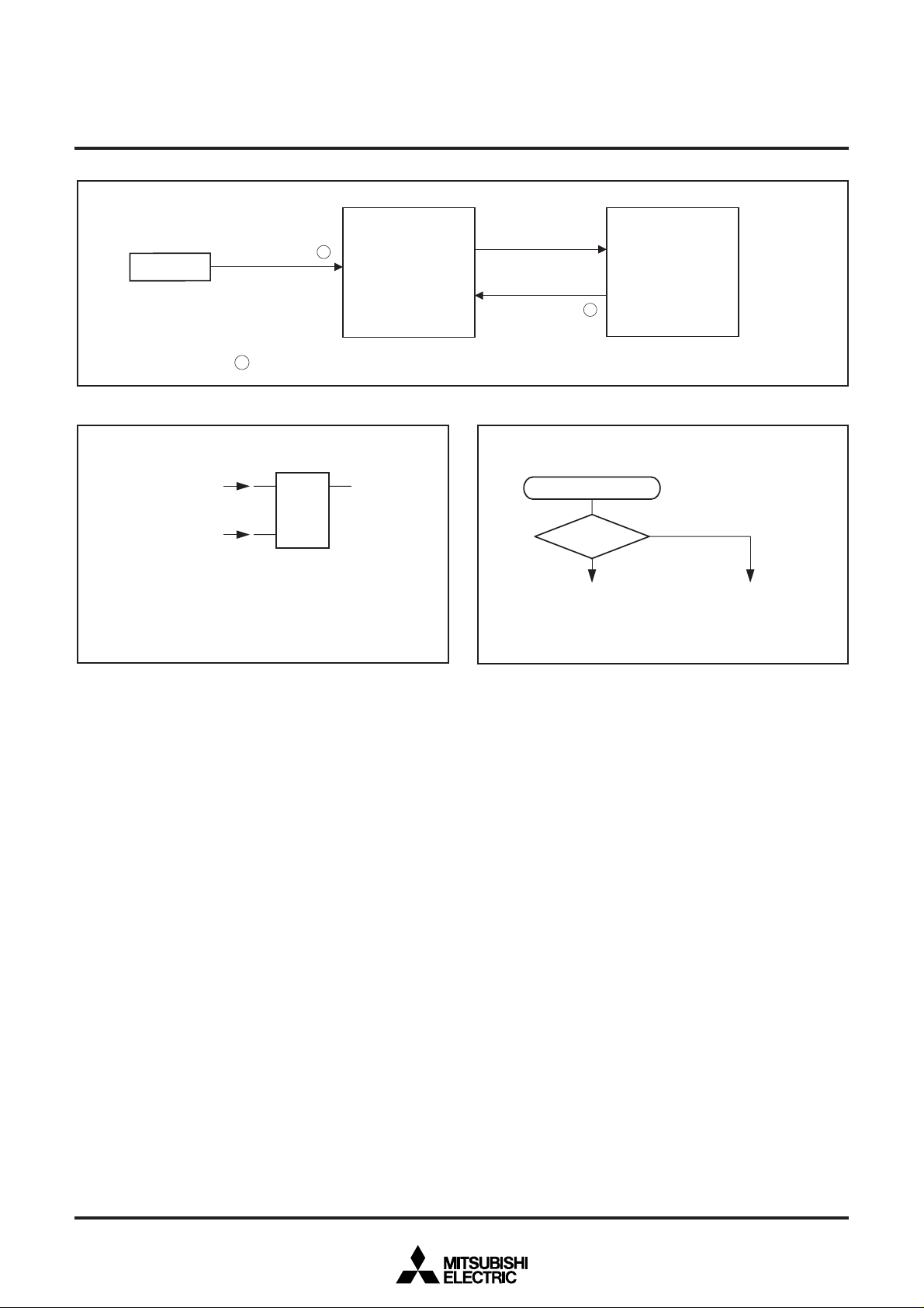
PRELIMINARY
Notice: This is not a final specification.
Some parametric limits are subject to
change.
MITSUBISHI MICROCOMPUTERS
4513/4514 Group
SINGLE-CHIP 4-BIT CMOS MICROCOMPUTER
Reset
Stabilizing time a
Fig. 38 State transition
POF instruction
Reset input or
voltage drop detection
circuit output
● Set source POF instruction is executed
● Clear source Reset input
A
POF instruction
B
is executed
(Stabilizing time a )
IN
) oscillation
f(X
Return input
(Stabilizing time a )
IN
) stop
f(X
(RAM back-up
mode)
: Time required to stabilize the f(XIN) oscillation is automatically generated by hardware.
Power down flag P
SRQ
Software start
P = “1”
Yes
?
No
• • • • • • •
• • • • • •
Cold start
Warm start
Fig. 39 Set source and clear source of the P flag
Fig. 40 Start condition identified example using the SNZP in-
struction
53

MITSUBISHI MICROCOMPUTERS
PRELIMINARY
Notice: This is not a final specification.
Some parametric limits are subject to
change.
Table 22 Key-on wakeup control register, pull-up control register, and interrupt control register
SINGLE-CHIP 4-BIT CMOS MICROCOMPUTER
4513/4514 Group
Key-on wakeup control register K0
K03
K02
K01
K00
PU03
PU02
PU01
PU00
I13
I12
I11
I10
Pins P12 and P13 key-on wakeup
control bit
Pins P10 and P11 key-on wakeup
control bit
Pins P02 and P03 key-on wakeup
control bit
Pins P00 and P01 key-on wakeup
control bit
Pull-up control register PU0 at reset : 00002 at RAM back-up : state retained
Pins P12 and P13 pull-up transistor
control bit
Pins P10 and P11 pull-up transistor
control bit
Pins P02 and P03 pull-up transistor
control bit
Pins P00 and P01 pull-up transistor
control bit
Interrupt control register I1
Not used
Interrupt valid waveform for INT0 pin/
return level selection bit (Note 2)
INT0 pin edge detection circuit control bit
INT0 pin
timer 1 control enable bit
at reset : 00002 at RAM back-up : state retained
0
Key-on wakeup not used
1
Key-on wakeup used
0
Key-on wakeup not used
1
Key-on wakeup used
0
Key-on wakeup not used
1
Key-on wakeup used
0
Key-on wakeup not used
1
Key-on wakeup used
0
Pull-up transistor OFF
1
Pull-up transistor ON
0
Pull-up transistor OFF
1
Pull-up transistor ON
0
Pull-up transistor OFF
1
Pull-up transistor ON
0
Pull-up transistor OFF
1
Pull-up transistor ON
at reset : 00002
0
This bit has no function, but read/write is enabled.
1
Falling waveform (“L” level of INT0 pin is recognized with the SNZI0
0
instruction)/“L” level
Rising waveform (“H” level of INT0 pin is recognized with the SNZI0
1
instruction)/“H” level
0
One-sided edge detected
1
Both edges detected
0
Disabled
1
Enabled
at RAM back-up : state retained
R/W
R/W
R/W
Interrupt control register I2
I23
I22
I21
I20
Notes 1: “R” represents read enabled, and “W” represents write enabled.
54
Not used
Interrupt valid waveform for INT1 pin/
return level selection bit (Note 3)
INT1 pin edge detection circuit control bit
INT1 pin
timer 3 control enable bit
2: When the contents of I1
3: When the contents of I2
2 is changed, the external interrupt request flag EXF0 may be set. Accordingly, clear EXF0 flag with the SNZ0 instruction.
2 is changed, the external interrupt request flag EXF1 may be set. Accordingly, clear EXF1 flag with the SNZ1 instruction.
0
1
0
1
0
1
0
1
at reset : 00002
This bit has no function, but read/write is enabled.
Falling waveform (“L” level of INT1 pin is recognized with the SNZI1
instruction)/“L” level
Rising waveform (“H” level of INT1 pin is recognized with the SNZI1
instruction)/“H” level
One-sided edge detected
Both edges detected
Disabled
Enabled
at RAM back-up : state retained
R/W

PRELIMINARY
Notice: This is not a final specification.
Some parametric limits are subject to
change.
MITSUBISHI MICROCOMPUTERS
4513/4514 Group
SINGLE-CHIP 4-BIT CMOS MICROCOMPUTER
CLOCK CONTROL
The clock control circuit consists of the following circuits.
• System clock generating circuit
• Control circuit to stop the clock oscillation
MR
X
IN
Oscillation
X
OUT
circuit
POF instruction
Division circuit
(divided by 2)
R
Q
S
• Control circuit to switch the middle-speed mode and high-speed
mode
• Control circuit to return from the RAM back-up state
3
1
Internal clock
generation circuit
0
(divided by 3)
RESET
System clock
Instruction clock
Counter
Wait time (Note)
control circuit
Software
start signal
Key-on wake up control register
K0
0
Falling detected
I1
2
“L” level
0
1
“H” level
,K01,K02,K0
Multiplexer
P30/INT
3
Ports P00, P0
Ports P02, P0
Ports P10, P1
Ports P12, P1
0
1
3
1
3
I2
2
“L” level
0
1
“H” level
P31/INT
1
Note: The wait time control circuit is used to generate the time required to stabilize the f(XIN) oscillation.
Fig. 41 Clock control circuit structure
Table 23 Clock control register MR
Clock control register MR
MR3
MR2
MR1
MR0
Note : “R” represents read enabled, and “W” represents write enabled.
System clock selection bit
Not used
Not used
Not used
at reset : 10002 at RAM back-up : 10002
0
f(XIN) (high-speed mode)
1
f(XIN)/2 (middle-speed mode)
0
This bit has no function, but read/write is enabled.
1
0
This bit has no function, but read/write is enabled.
1
0
This bit has no function, but read/write is enabled.
1
R/W
55

PRELIMINARY
4513/4514
X
IN
X
OUT
Rd
C
IN
C
OUT
Notice: This is not a final specification.
Some parametric limits are subject to
change.
Clock signal f(XIN) is obtained by externally connecting a ceramic
resonator.
Connect this external circuit to pins XIN and XOUT at the shortest
distance. A feedback resistor is built in between pins XIN and XOUT.
When an external clock signal is input, connect the clock source to
XIN and leave XOUT open. When using an external clock, the maximum value of external clock oscillating frequency is shown in Table
24.
MITSUBISHI MICROCOMPUTERS
4513/4514 Group
SINGLE-CHIP 4-BIT CMOS MICROCOMPUTER
Note: Externally connect a
damping resistor Rd depending on the oscillation
frequency.
(A feedback resistor is
built-in.)
Use the resonator manufacturer’s recommended
value because constants
such as capacitance depend on the resonator.
Fig. 42 Ceramic resonator external circuit
4513/4514
Table 24 Maximum value of external clock oscillation frequency
Middle-speed mode
Mask ROM version
High-speed mode
Middle-speed mode
One Time PROM version
High-speed mode
ROM ORDERING METHOD
Please submit the information described below when ordering
Mask ROM.
(1) Mask ROM Order Confirmation Form ..................................... 1
(2) Data to be written into mask ROM ...............................EPROM
(three sets containing the identical data)
(3) Mark Specification Form .......................................................... 1
X
IN
X
OUT
External oscillation circuit
Fig. 43 External clock input circuit
Supply voltage
VDD = 2.0 V to 5.5 V
VDD = 4.0 V to 5.5 V
VDD = 2.5 V to 5.5 V
VDD = 2.0 V to 5.5 V
VDD = 2.5 V to 5.5 V
VDD = 4.0 V to 5.5 V
VDD = 2.5 V to 5.5 V
VDD
VSS
Oscillation frequency (duty ratio)
3.0 MHz (40 % to 60 %)
3.0 MHz (40 % to 60 %)
1.0 MHz (40 % to 60 %)
0.8 MHz (40 % to 60 %)
3.0 MHz (40 % to 60 %)
3.0 MHz (40 % to 60 %)
1.0 MHz (40 % to 60 %)
56

PRELIMINARY
Notice: This is not a final specification.
Some parametric limits are subject to
change.
MITSUBISHI MICROCOMPUTERS
4513/4514 Group
SINGLE-CHIP 4-BIT CMOS MICROCOMPUTER
LIST OF PRECAUTIONS
➀Noise and latch-up prevention
Connect a capacitor on the following condition to prevent noise
and latch-up;
• connect a bypass capacitor (approx. 0.1
and VSS at the shortest distance,
• equalize its wiring in width and length, and
• use relatively thick wire.
In the One Time PROM version, CNVSS pin is also used as VPP
pin. Accordingly, when using this pin, connect this pin to VSS
through a resistor about 5 kΩ in series at the shortest distance.
➁ Prescaler
Stop the prescaler operation to change its frequency dividing ratio.
➂ Timer count source
Stop timer 1, 2, 3, or 4 counting to change its count source.
➃ Reading the count value
Stop timer 1, 2, 3, or 4 counting and then execute the TAB1,
TAB2, TAB3, or TAB4 instruction to read its data.
➄ Writing to reload registers R1 and R3
When writing data to reload registers R1 or R3 while timer 1 or
timer 3 is operating, avoid a timing when timer 1 or timer 3
underflows.
➅P30/INT0 pin
When the interrupt valid waveform of the P30/INT0 pin is
changed with the bit 2 of register I1 in software, be careful about
the following notes.
• Clear the bit 0 of register V1 to “0” before the interrupt valid waveform of P30/INT0 pin is changed with the bit 2 of register I1 (refer
to Figure 44➀).
• Depending on the input state of the P30/INT0 pin, the external 0
interrupt request flag (EXF0) may be set when the interrupt valid
waveform is changed. Accordingly, clear bit 2 of register I1, and
execute the SNZ0 instruction to clear the EXF0 flag after executing at least one instruction (refer to Figure 44➁)
µ
F) between pins VDD
➆ P31/INT1 pin
When the interrupt valid waveform of P31/INT1 pin is changed
with the bit 2 of register I2 in software, be careful about the following notes.
• Clear the bit 1 of register V1 to “0” before the interrupt valid waveform of P31/INT1 pin is changed with the bit 2 of register I2 (refer
to Figure 45➂).
• Depending on the input state of the P31/INT1 pin, the external 1
interrupt request flag (EXF1) may be set when the interrupt valid
waveform is changed. Accordingly, clear bit 2 of register I2 and
execute the SNZ1 instruction to clear the EXF1 flag after executing at least one instruction (refer to Figure 45➃).
.
.
.
LA 8 ; (✕✕0✕2)
TV1A ; The SNZ1 instruction is valid...........➂
LA 8
TI2A ; Change of the interrupt valid waveform
NOP ........................................................... ➃
SNZ1 ; The SNZ1 instruction is executed
NOP
.
.
.
✕ : this bit is not related to the setting of INT1.
Fig. 45 External 1 interrupt program example
➇ One Time PROM version
The operating power voltage of the One Time PROM version is
2.5 V to 5.5 V.
➈ Multifunction
The input of D6, D7, P20–P22, I/O of P30 and P31, input of CMP0-,
CMP0+, CMP1-, CMP1+, and I/O of P40–P43 can be used even
when CNTR0, CNTR1, SCK, SOUT, SIN, INT0, INT1, AIN0–AIN3
and AIN4–AIN7 are selected.
.
.
.
LA 4 ; (✕✕✕02)
TV1A ; The SNZ0 instruction is valid...........➀
LA 4 ;
TI1A ; Interrupt valid waveform is changed
NOP ........................................................... ➁
SNZ0 ; The SNZ0 instruction is executed
NOP
.
.
.
✕ : this bit is not related to the setting of INT0 pin.
Fig. 44 External 0 interrupt program example
57

PRELIMINARY
Notice: This is not a final specification.
Some parametric limits are subject to
change.
➉ A-D converter-1
When the operating mode of the A-D converter is changed from
the comparator mode to the A-D conversion mode with the bit 3
of register Q2 in a program, be careful about the following notes.
• Clear the bit 2 of register V2 to “0” to change the operating mode
of the A-D converter from the comparator mode to the A-D conversion mode with the bit 3 of register Q2 (refer to Figure 46➄).
• The A-D conversion completion flag (ADF) may be set when the
operating mode of the A-D converter is changed from the comparator mode to the A-D conversion mode. Accordingly, set a
value to register Q2, and execute the SNZAD instruction to clear
the ADF flag.
Do not change the operating mode (both A-D conversion mode
and comparator mode) of A-D converter with the bit 3 of register
Q2 during operating the A-D converter.
.
.
.
LA 8 ; (✕0✕✕2)
TV2A ; The SNZAD instruction is valid ........➄
LA 0 ; (0✕✕✕2)
TQ2A ; Change of the operating mode of the A-D
converter from the comparator mode to the
A-D conversion mode
SNZAD
NOP
.
.
.
Fig. 46 A-D converter operating mode program example
11
A-D converter-2
Each analog input pin is equipped with a capacitor which is used
to compare the analog voltage. Accordingly, when the analog
voltage is input from the circuit with high-impedance and, charge/
discharge noise is generated and the sufficient A-D accuracy
may not be obtained. Therefore, reduce the impedance or, connect a capacitor (0.01 µF to 1 µF) to analog input pins (Figure
47).
When the overvoltage applied to the A-D conversion circuit may
occur, connect an external circuit in order to keep the voltage
within the rated range as shown the Figure 48. In addition, test
the application products sufficiently.
✕: this bit is not related to the change of the
operating mode of the A-D conversion.
MITSUBISHI MICROCOMPUTERS
4513/4514 Group
SINGLE-CHIP 4-BIT CMOS MICROCOMPUTER
Sensor
Apply the voltage withiin the specifications
to an analog input pin.
Fig. 47 Analog input external circuit example-1
Sensor
Fig. 48 Analog input external circuit example-2
12
POF instruction
Execute the POF instruction immediately after executing the
EPOF instruction to enter the RAM back-up.
Note that system cannot enter the RAM back-up state when executing only the POF instruction.
Be sure to disable interrupts by executing the DI instruction before executing the EPOF instruction.
13
Analog input pins
Note the following when using the analog input pins also for I/O
port P4 functions:
• Even when P40/AIN4–P43/AIN7 are set to pins for analog input,
they continue to function as P40–P43 I/O. Accordingly, when any
of them are used as I/O port P4 and others are used as analog
input pins, make sure to set the outputs of pins that are set for
analog input to “1.” Also, the port input function of the pin functions as an analog input is undefined.
• TALA instruction
When the TALA instruction is executed, the low-order 2 bits of
register AD is transferred to the high-order 2 bits of register A, simultaneously, the low-order 2 bits of register A is “0.”
About 1kΩ
A
IN
A
IN
58
14
Program counter
Make sure that the PCH does not specify after the last page of
the built-in ROM.
15
Port P3
In the 4513 Group, when the IAP3 instruction is executed, note
that the high-order 2 bits of register A is undefined.

PRELIMINARY
Notice: This is not a final specification.
Some parametric limits are subject to
change.
16
Voltage comparator function
When the voltage comparator function is valid with the voltage
comparator control register Q3, it is operating even in the RAM
back-up mode. Accordingly, be careful about such state because
it causes the increase of the operation current in the RAM backup mode.
In order to reduce the operation current in the RAM back-up
mode, invalidate (bits 2 and 3 of register Q3 = “0”) the voltage
comparator function by software before the POF instruction is executed.
Also, while the voltage comparator function is valid, current is always consumed by voltage comparator. On the system required
for the low-power dissipation, invalidate the voltage comparator
when it is unused by software.
17
Register Q3
Bits 0 and 1 of register Q3 can be only read. Note that they cannot be written.
MITSUBISHI MICROCOMPUTERS
4513/4514 Group
SINGLE-CHIP 4-BIT CMOS MICROCOMPUTER
18
Reading the comparison result of voltage comparator
Read the voltage comparator comparison result from register Q3
after the voltage comparator response time (max. 20 µs) is
passed from the voltage comparator function become valid.
59

MITSUBISHI MICROCOMPUTERS
4513/4514 Group
PRELIMINARY
Notice: This is not a final specification.
Some parametric limits are subject to
change.
SYMBOL
The symbols shown below are used in the following instruction function table and instruction list.
Symbol
A
B
DR
E
Q1
Q2
Q3
AD
J1
SI
V1
V2
I1
I2
W1
W2
W3
W4
W6
MR
K0
PU0
FR0
X
Y
Z
DP
PC
PCH
PCL
SK
SP
CY
R1
R2
R3
R4
T1
T2
T3
T4
Note : The 4513/4514 Group just invalidates the next instruction when a skip is performed. The contents of program counter is not increased by 2. Accord-
ingly, the number of cycles does not change even if skip is not performed. However, the cycle count becomes “1” if the TABP p, RT, or RTS instruction
is skipped.
Register A (4 bits)
Register B (4 bits)
Register D (3 bits)
Register E (8 bits)
A-D control register Q1 (4 bits)
A-D control register Q2 (4 bits)
Voltage comparator control register Q3 (4 bits)
Successive comparison register AD (10 bits)
Serial I/O mode register J1 (4 bits)
Serial I/O register SI (8 bits)
Interrupt control register V1 (4 bits)
Interrupt control register V2 (4 bits)
Interrupt control register I1 (4 bits)
Interrupt control register I2 (4 bits)
Timer control register W1 (4 bits)
Timer control register W2 (4 bits)
Timer control register W3 (4 bits)
Timer control register W4 (4 bits)
Timer control register W6 (4 bits)
Clock control register MR (4 bits)
Key-on wakeup control register K0 (4 bits)
Pull-up control register PU0 (4 bits)
Direction register FR0 (4 bits)
Register X (4 bits)
Register Y (4 bits)
Register Z (2 bits)
Data pointer (10 bits)
(It consists of registers X, Y, and Z)
Program counter (14 bits)
High-order 7 bits of program counter
Low-order 7 bits of program counter
Stack register (14 bits ✕ 8)
Stack pointer (3 bits)
Carry flag
Timer 1 reload register
Timer 2 reload register
Timer 3 reload register
Timer 4 reload register
Timer 1
Timer 2
Timer 3
Timer 4
Contents
Symbol
T1F
T2F
T3F
T4F
WDF1
WEF
INTE
EXF0
EXF1
P
ADF
SIOF
D
P0
P1
P2
P3
P4
P5
x
y
z
p
n
i
j
A3A2A1A0
←
↔
?
( )
—
M(DP)
a
p, a
C
+
x
SINGLE-CHIP 4-BIT CMOS MICROCOMPUTER
Contents
Timer 1 interrupt request flag
Timer 2 interrupt request flag
Timer 3 interrupt request flag
Timer 4 interrupt request flag
Watchdog timer flag
Watchdog timer enable flag
Interrupt enable flag
External 0 interrupt request flag
External 1 interrupt request flag
Power down flag
A-D conversion completion flag
Serial I/O transmission/reception completion flag
Port D (8 bits)
Port P0 (4 bits)
Port P1 (4 bits)
Port P2 (3 bits)
Port P3 (4 bits)
Port P4 (4 bits)
Port P5 (4 bits)
Hexadecimal variable
Hexadecimal variable
Hexadecimal variable
Hexadecimal variable
Hexadecimal constant
Hexadecimal constant
Hexadecimal constant
Binary notation of hexadecimal variable A
(same for others)
Direction of data movement
Data exchange between a register and memory
Decision of state shown before “?”
Contents of registers and memories
Negate, Flag unchanged after executing instruction
RAM address pointed by the data pointer
Label indicating address a6 a5 a4 a3 a2 a1 a0
Label indicating address a6 a5 a4 a3 a2 a1 a0
in page p5 p4 p3 p2 p1 p0
Hex. C + Hex. number x (also same for others)
60

PRELIMINARY
Notice: This is not a final specification.
Some parametric limits are subject to
change.
LIST OF INSTRUCTION FUNCTION
Group-
Mnemonic
ing
TAB
TBA
TAY
TYA
TEAB
TABE
TDA
TAD
Register to register transfer
TAZ
TAX
TASP
LXY x, y
LZ z
INY
RAM addresses
DEY
TAM j
XAM j
XAMD j
RAM to register transfer
(A) ← (B)
(B) ← (A)
(A) ← (Y)
(Y) ← (A)
(E7–E4) ← (B)
(E3–E0) ← (A)
(B) ← (E7–E4)
(A) ← (E3–E0)
(DR2–DR0) ← (A2–A0)
(A2–A0) ← (DR2–DR0)
(A3) ← 0
(A1, A0) ← (Z1, Z0)
(A3, A2) ← 0
(A) ← (X)
(A2–A0) ← (SP2–SP0)
(A3) ← 0
(X) ← x, x = 0 to 15
(Y) ← y, y = 0 to 15
(Z) ← z, z = 0 to 3
(Y) ← (Y) + 1
(Y) ← (Y) – 1
(A) ← (M(DP))
(X) ← (X)EXOR(j)
j = 0 to 15
(A) ← → (M(DP))
(X) ← (X)EXOR(j)
j = 0 to 15
(A) ← → (M(DP))
(X) ← (X)EXOR(j)
j = 0 to 15
(Y) ← (Y) – 1
Function
Group-
Mnemonic
ing
XAMI j
TMA j
RAM to register transfer
LA n
TABP p
AM
AMC
A n
AND
Arithmetic operation
OR
SC
RC
SZC
CMA
RAR
(A) ← → (M(DP))
(X) ← (X)EXOR(j)
j = 0 to 15
(Y) ← (Y) + 1
(M(DP)) ← (A)
(X) ← (X)EXOR(j)
j = 0 to 15
(A) ← n
n = 0 to 15
(SP) ← (SP) + 1
(SK(SP)) ← (PC)
(PCH) ← p
(PCL) ← (DR2–DR0,
A3–A0)
(B) ← (ROM(PC))7–4
(A) ← (ROM(PC))3–0
(PC) ← (SK(SP))
(SP) ← (SP) – 1
(A) ← (A) + (M(DP))
(A) ← (A) + (M(DP)) +
(CY)
(CY) ← Carry
(A) ← (A) + n
n = 0 to 15
(A) ← (A) AND (M(DP))
(A) ← (A) OR (M(DP))
(CY) ← 1
(CY) ← 0
(CY) = 0 ?
(A) ← (A)
→ CY → A3A2A1A0
MITSUBISHI MICROCOMPUTERS
4513/4514 Group
SINGLE-CHIP 4-BIT CMOS MICROCOMPUTER
Function
Group-
Mnemonic
ing
SB j
RB j
Bit operation
SZB j
SEAM
SEA n
operation
Comparison
B a
BL p, a
BLA p
Branch operation
BM a
BML p, a
BMLA p
Subroutine operation
RTI
RT
RTS
Return operation
(Mj(DP)) ← 1
j = 0 to 3
(Mj(DP)) ← 0
j = 0 to 3
(Mj(DP)) = 0 ?
j = 0 to 3
(A) = (M(DP)) ?
(A) = n ?
n = 0 to 15
(PCL) ← a6–a0
(PCH) ← p
(PCL) ← a6–a0
(PCH) ← p
(PCL) ← (DR2–DR0,
A3–A0)
(SP) ← (SP) + 1
(SK(SP)) ← (PC)
(PCH) ← 2
(PCL) ← a6–a0
(SP) ← (SP) + 1
(SK(SP)) ← (PC)
(PCH) ← p
(PCL) ← a6–a0
(SP) ← (SP) + 1
(SK(SP)) ← (PC)
(PCH) ← p
(PCL) ← (DR2–DR0,
A3–A0)
(PC) ← (SK(SP))
(SP) ← (SP) – 1
(PC) ← (SK(SP))
(SP) ← (SP) – 1
(PC) ← (SK(SP))
(SP) ← (SP) – 1
Function
61

PRELIMINARY
Notice: This is not a final specification.
Some parametric limits are subject to
change.
MITSUBISHI MICROCOMPUTERS
4513/4514 Group
SINGLE-CHIP 4-BIT CMOS MICROCOMPUTER
LIST OF INSTRUCTION FUNCTION (continued)
Group-
Mnemonic
ing
DI
EI
SNZ0
SNZ1
SNZI0
SNZI1
TAV1
Interrupt operation
TV1A
TAV2
Function
(INTE) ← 0
(INTE) ← 1
(EXF0) = 1 ?
After skipping
(EXF0) ← 0
(EXF1) = 1 ?
After skipping
(EXF1) ← 0
I12 = 1 : (INT0) = “H” ?
I12 = 0 : (INT0) = “L” ?
I22 = 1 : (INT1) = “H” ?
I22 = 0 : (INT1) = “L” ?
(A) ← (V1)
(V1) ← (A)
(A) ← (V2)
Group-
ing
Mnemonic
TAW4
TW4A
TAW6
TW6A
TAB1
T1AB
TAB2
T2AB
Function
(A) ← (W4)
(W4) ← (A)
(A) ← (W6)
(W6) ← (A)
(B) ← (T17–T14)
(A) ← (T13–T10)
(R17–R14) ← (B)
(T17–T14) ← (B)
(R13–R10) ← (A)
(T13–T10) ← (A)
(B) ← (T27–T24)
(A) ← (T23–T20)
(R27–R24) ← (B)
(T27–T24) ← (B)
(R23–R20) ← (A)
(T23–T20) ← (A)
Group-
ing
Timer operation
Mnemonic
SNZT1
SNZT2
SNZT3
SNZT4
IAP0
OP0A
IAP1
OP1A
Function
(T1F) = 1 ?
After skipping
(T1F) ← 0
(T2F) = 1 ?
After skipping
(T2F) ← 0
(T3F) = 1 ?
After skipping
(T3F) ← 0
(T4F) = 1 ?
After skipping
(T4F) ← 0
(A) ← (P0)
(P0) ← (A)
(A) ← (P1)
(P1) ← (A)
TV2A
TAI1
TI1A
TAI2
TI2A
TAW1
TW1A
TAW2
TW2A
TAW3
Timer operation
TW3A
(V2) ← (A)
(A) ← (I1)
(I1) ← (A)
(A) ← (I2)
(I2) ← (A)
(A) ← (W1)
(W1) ← (A)
(A) ← (W2)
(W2) ← (A)
(A) ← (W3)
(W3) ← (A)
TAB3
Timer operation
T3AB
TAB4
T4AB
TR1AB
TR3AB
(B) ← (T37–T34)
(A) ← (T33–T30)
(R37–R34) ← (B)
(T37–T34) ← (B)
(R33–R30) ← (A)
(T33–T30) ← (A)
(B) ← (T47–T44)
(A) ← (T43–T40)
(R47–R44) ← (B)
(T47–T44) ← (B)
(R43–R40) ← (A)
(T43–T40) ← (A)
(R17–R14) ← (B)
(R13–R10) ← (A)
(R37–R34) ← (B)
(R33–R30) ← (A)
IAP2
IAP3
OP3A
IAP4*
OP4A*
IAP5*
Input/Output operation
OP5A*
CLD
RD
SD
SZD
(A2–A0) ← (P22–P20)
(A3) ← 0
(A) ← (P3)
(P3) ← (A)
(A) ← (P4)
(P4) ← (A)
(A) ← (P5)
(P5) ← (A)
(D) ← 1
(D(Y)) ← 0
(Y) = 0 to 7
(D(Y)) ← 1
(Y) = 0 to 7
(D(Y)) = 0 ?
(Y) = 0 to 7
*: The 4513 Group does not have these instructions.
62

PRELIMINARY
Notice: This is not a final specification.
Some parametric limits are subject to
change.
MITSUBISHI MICROCOMPUTERS
4513/4514 Group
SINGLE-CHIP 4-BIT CMOS MICROCOMPUTER
LIST OF INSTRUCTION FUNCTION (continued)
Group-
Mnemonic
ing
TK0A
TAK0
TPU0A
TAPU0
Input/Output operation
TFR0A*
TABSI
TSIAB
TAJ1
TJ1A
SST
Serial I/O control operation
(K0) ← (A)
(A) ← (K0)
(PU0) ← (A)
(A) ← (PU0)
(FR0) ← (A)
(A) ← (SI3–SI0)
(B) ← (SI7–SI4)
(SI3–SI0) ← (A)
(SI7–SI4) ← (B)
(A) ← (J1)
(J1) ← (A)
(SIOF) ← 0
Serial I/O starting
Function
Group-
Mnemonic
ing
TABAD
TALA
TADAB
TAQ1
TQ1A
ADST
A-D conversion operation
SNZAD
Function
(A) ← (AD5–AD2)
(B) ← (AD9–AD6)
However, in the com-
parator mode,
(A) ← (AD3–AD0)
(B) ← (AD7–AD4)
(A) ← (AD1, AD0, 0, 0)
(AD3–AD0) ← (A)
(AD7–AD4) ← (B)
(A) ← (Q1)
(Q1) ← (A)
(ADF) ← 0
A-D conversion starting
(ADF) = 1 ?
After skipping
(ADF) ← 0
SNZSI
(SIOF) = 1 ?
After skipping
(SIOF) ← 0
TAQ2
TQ2A
NOP
POF
EPOF
SNZP
WRST
TAMR
Other operation
TMRA
TAQ3
TQ3A
(A) ← (Q2)
(Q2) ← (A)
(PC) ← (PC) + 1
RAM back-up
POF instruction valid
(P) = 1 ?
(WDF1) ← 0, (WEF) ← 1
(A) ← (MR)
(MR) ← (A)
(A) ← (Q3)
(Q33, Q32) ← (A3, A2)
(Q31) ← (CMP1 com-
parison result)
(Q30) ← (CMP0 com-
parison result)
*: The 4513 Group does not have these instructions.
63

MITSUBISHI MICROCOMPUTERS
4513/4514 Group
PRELIMINARY
Notice: This is not a final specification.
Some parametric limits are subject to
change.
INSTRUCTION CODE TABLE (for 4513 Group)
D9–D4
Hex.
D3–D0
notation
0000
0001
0010
0011
0100
0101
0110
0111
1000
1001
1010
1011
1100
1101
1110
1111
The above table shows the relationship between machine language codes and machine language instructions. D3–D0 show the low-order
4 bits of the machine language code, and D9–D4 show the high-order 6 bits of the machine language code. The hexadecimal representation of the code is also provided. There are one-word instructions and two-word instructions, but only the first word of each instruction is
shown. Do not use code marked “–.”
0
1
2
3
4
5
6
7
8
9
A
B
C
D
E
F
000000
00
NOP
–
POF
SNZP
DI
EI
RC
SC
–
–
AM
AMC
TYA
–
TBA
–
000001
01
BLA
CLD
–
INY
RD
SD
–
DEY
AND
OR
TEAB
–
CMA
RAR
TAB
TAY
000010
02
SZB
0
SZB
1
SZB
2
SZB
3
SZD
SEAn
SEAM
–
–
TDA
TABE
–
–
–
–
SZC
000011
03
BMLA
–
–
–
–
–
–
–
SNZ0
SNZ1
SNZI0
SNZI1
–
–
TV2A
TV1A
000100
04
–
–
–
–
RT
RTS
RTI
–
LZ
0
LZ
1
LZ
2
LZ
3
RB
0
RB
1
RB
2
RB
3
000101
05
TASP
TAD
TAX
TAZ
TAV1
TAV2
–
–
–
–
–
EPOF
SB
0
SB
1
SB
2
SB
3
000110
06
A
0
A
1
A
2
A
3
A
4
A
5
A
6
A
7
A
8
A
9
A
10
A
11
A
12
A
13
A
14
A
15
000111
07
LA
0
LA
1
LA
2
LA
3
LA
4
LA
5
LA
6
LA
7
LA
8
LA
9
LA
10
LA
11
LA
12
LA
13
LA
14
LA
15
001000
08
TABP
0
TABP
1
TABP
2
TABP
3
TABP
4
TABP
5
TABP
6
TABP
7
TABP
8
TABP
9
TABP
10
TABP
11
TABP
12
TABP
13
TABP
14
TABP
15
SINGLE-CHIP 4-BIT CMOS MICROCOMPUTER
0B
TABP
48*
TABP
49*
TABP
50*
TABP
51*
TABP
52*
TABP
53*
TABP
54*
TABP
55*
TABP
56*
TABP
57*
TABP
58*
TABP
59*
TABP
60*
TABP
61*
TABP
62*
TABP
63*
001100
0011010D0011100E001111
0C
BML
BML***
BML
BML***
BML
BML***
BML
BML***
BML
BML***
BML
BML***
BML
BML***
BML
BML***
BML
BML***
BML
BML***
BML
BML***
BML
BML***
BML
BML***
BML
BML***
BML
BML***
BML
BML***
BL
BL
BL
BL
BL
BL
BL
BL
BL
BL
BL
BL
BL
BL
BL
BL
0F
BL***
BL***
BL***
BL***
BL***
BL***
BL***
BL***
BL***
BL***
BL***
BL***
BL***
BL***
BL***
BL***
001001
09
TABP
16***
TABP
17***
TABP
18***
TABP
19***
TABP
20***
TABP
21***
TABP
22***
TABP
23***
TABP
24***
TABP
25***
TABP
26***
TABP
27***
TABP
28***
TABP
29***
TABP
30***
TABP
31***
0010100A001011
TABP
32**
TABP
33**
TABP
34**
TABP
35**
TABP
36**
TABP
37**
TABP
38**
TABP
39**
TABP
40**
TABP
41**
TABP
42**
TABP
43**
TABP
44**
TABP
45**
TABP
46**
TABP
47**
010000
010111
10–17
BM
BM
BM
BM
BM
BM
BM
BM
BM
BM
BM
BM
BM
BM
BM
BM
011000
011111
18–1F
B
B
B
B
B
B
B
B
B
B
B
B
B
B
B
B
The codes for the second word of a two-word instruction are described below.
BL
BML
BLA
BMLA
SEA
SZD
64
The second word
10 paaa aaaa
10 paaa aaaa
10 pp00 pppp
10 pp00 pppp
00 0111 nnnn
00 0010 1011
• *, **, and *** cannot be used in the M34513M2-XXXSP/FP.
• * and ** cannot be used in the M34513M4-XXXSP/FP.
• * and ** cannot be used in the M34513E4FP.
• * cannot be used in the M34513M6-XXXFP.

MITSUBISHI MICROCOMPUTERS
4513/4514 Group
PRELIMINARY
Notice: This is not a final specification.
Some parametric limits are subject to
change.
INSTRUCTION CODE TABLE (continued) (for 4513 Group)
D9–D4
Hex.
D3–D0
notation
0000
0001
0010
0011
0100
0101
0110
0111
1000
1001
1010
1011
1100
1101
1110
1111
The above table shows the relationship between machine language codes and machine language instructions. D3–D0 show the loworder 4 bits of the machine language code, and D9–D4 show the high-order 6 bits of the machine language code. The hexadecimal
representation of the code is also provided. There are one-word instructions and two-word instructions, but only the first word of
each instruction is shown. Do not use code marked “–.”
0
1
2
3
4
5
6
7
8
9
A
B
C
D
E
F
1000012110001022100011231001002410010125100110261001112710100028101001291010102A101011
100000
20
–
–
TJ1A
–
TQ1A
TQ2A
TQ3A
–
–
–
–
–
–
–
TW1A
TW2A
TW3A
TW4A
–
TW6A
–
–
TMRA
TI1A
TI2A
–
–
TK0A
–
–
–
–
OP0A
OP1A
–
OP3A
–
–
–
–
–
–
–
–
–
TPU0A
–
–
T1AB
T2AB
T3AB
T4AB
–
–
–
–
TSIAB
T ADAB
–
TR3AB
–
–
–
TR1AB
–
–
TAJ1
–
TAQ1
TAQ2
TAQ3
–
–
TALA
–
TAW1
TAW2
TAW3
TAW4
–
TAW6
–
TAMR
TAI1
TAI2
–
TAK0
TAPU0
–
–
–
–
–
–
–
–
IAP0
IAP1
IAP2
IAP3
–
–
–
–
–
–
–
–
–
–
–
–
TAB1
TAB2
TAB3
TAB4
–
–
–
–
TABSI
TABAD
–
–
–
–
–
–
SNZT1
SNZT2
SNZT3
SNZT4
–
–
–
SNZAD
SNZSI
–
–
–
–
–
–
–
SINGLE-CHIP 4-BIT CMOS MICROCOMPUTER
101100
1011012D1011102E101111
2B
–
–
–
–
–
–
–
–
–
–
–
–
–
–
SST
ADST
WRST
–
–
–
–
–
–
–
–
–
–
–
–
–
–
–
TMA
0
TMA
1
TMA
2
TMA
3
TMA
4
TMA
5
TMA
6
TMA
7
TMA
8
TMA
9
TMA
10
TMA
11
TMA
12
TMA
13
TMA
14
TMA
15
2C
TAM
0
TAM
1
TAM
2
TAM
3
TAM
4
TAM
5
TAM
6
TAM
7
TAM
8
TAM
9
TAM
10
TAM
11
TAM
12
TAM
13
TAM
14
TAM
15
XAM
0
XAM
1
XAM
2
XAM
3
XAM
4
XAM
5
XAM
6
XAM
7
XAM
8
XAM
9
XAM
10
XAM
11
XAM
12
XAM
13
XAM
14
XAM
15
XAMI
0
XAMI
1
XAMI
2
XAMI
3
XAMI
4
XAMI
5
XAMI
6
XAMI
7
XAMI
8
XAMI
9
XAMI
10
XAMI
11
XAMI
12
XAMI
13
XAMI
14
XAMI
15
2F
XAMD
0
XAMD
1
XAMD
2
XAMD
3
XAMD
4
XAMD
5
XAMD
6
XAMD
7
XAMD
8
XAMD
9
XAMD
10
XAMD
11
XAMD
12
XAMD
13
XAMD
14
XAMD
15
110000
111111
30–3F
LXY
LXY
LXY
LXY
LXY
LXY
LXY
LXY
LXY
LXY
LXY
LXY
LXY
LXY
LXY
LXY
The codes for the second word of a two-word instruction are described below.
The second word
BL
BML
BLA
BMLA
SEA
SZD
10 paaa aaaa
10 paaa aaaa
10 pp00 pppp
10 pp00 pppp
00 0111 nnnn
00 0010 1011
65

MITSUBISHI MICROCOMPUTERS
4513/4514 Group
PRELIMINARY
Notice: This is not a final specification.
Some parametric limits are subject to
change.
INSTRUCTION CODE TABLE (for 4514 Group)
D9–D4
0000
0001
0010
0011
0100
0101
0110
0111
1000
1001
1010
1011
1100
1101
1110
1111
Hex.
notation
0
1
2
3
4
5
6
7
8
9
A
B
C
D
E
F
D3–D0
The above table shows the relationship between machine language codes and machine language instructions. D3–D0 show the low-order
4 bits of the machine language code, and D9–D4 show the high-order 6 bits of the machine language code. The hexadecimal representation of the code is also provided. There are one-word instructions and two-word instructions, but only the first word of each instruction is
shown. Do not use code marked “–.”
0000010100001002000011030001000400010105000110060001110700100008001001090010100A001011
000000
00
A
LA
LA
LA
LA
LA
LA
LA
LA
LA
LA
LA
10
LA
11
LA
12
LA
13
LA
14
LA
15
TABP
0
0
TABP
1
1
TABP
2
2
TABP
3
3
TABP
4
4
TABP
5
5
TABP
6
6
TABP
7
7
TABP
8
8
TABP
9
9
TABP
10
TABP
11
TABP
12
TABP
13
TABP
14
TABP
15
NOP
–
POF
SNZP
DI
EI
RC
SC
–
–
AM
AMC
TYA
–
TBA
–
BLA
CLD
–
INY
RD
SD
–
DEY
AND
OR
TEAB
–
CMA
RAR
TAB
TAY
SZB
0
SZB
1
SZB
2
SZB
3
SZD
SEAn
SEAM
–
–
TDA
TABE
–
–
–
–
SZC
BMLA
–
–
–
–
–
–
–
SNZ0
SNZ1
SNZI0
SNZI1
–
–
TV2A
TV1A
–
–
–
–
RT
RTS
RTI
–
LZ
0
LZ
1
LZ
2
LZ
3
RB
0
RB
1
RB
2
RB
3
TASP
TAD
TAX
TAZ
TAV1
TAV2
–
–
–
–
–
EPOF
SB
0
SB
1
SB
2
SB
3
0
A
1
A
2
A
3
A
4
A
5
A
6
A
7
A
8
A
9
A
10
A
11
A
12
A
13
A
14
A
15
SINGLE-CHIP 4-BIT CMOS MICROCOMPUTER
001100
0011010D0011100E001111
0B
TABP
16
TABP
17
TABP
18
TABP
19
TABP
20
TABP
21
TABP
22
TABP
23
TABP
24
TABP
25
TABP
26
TABP
27
TABP
28
TABP
29
TABP
30
TABP
31
TABP
32
TABP
33
TABP
34
TABP
35
TABP
36
TABP
37
TABP
38
TABP
39
TABP
40
TABP
41
TABP
42
TABP
43
TABP
44
TABP
45
TABP
46
TABP
47
TABP
48*
TABP
49*
TABP
50*
TABP
51*
TABP
52*
TABP
53*
TABP
54*
TABP
55*
TABP
56*
TABP
57*
TABP
58*
TABP
59*
TABP
60*
TABP
61*
TABP
62*
TABP
63*
0C
BML
BML
BML
BML
BML
BML
BML
BML
BML
BML
BML
BML
BML
BML
BML
BML
BML
BML
BML
BML
BML
BML
BML
BML
BML
BML
BML
BML
BML
BML
BML
BML
BL
BL
BL
BL
BL
BL
BL
BL
BL
BL
BL
BL
BL
BL
BL
BL
0F
BL
BL
BL
BL
BL
BL
BL
BL
BL
BL
BL
BL
BL
BL
BL
BL
010000
010111
10–17
BM
BM
BM
BM
BM
BM
BM
BM
BM
BM
BM
BM
BM
BM
BM
BM
011000
011111
18–1F
B
B
B
B
B
B
B
B
B
B
B
B
B
B
B
B
The codes for the second word of a two-word instruction are described below.
BL
BML
BLA
BMLA
SEA
SZD
66
The second word
10 paaa aaaa
10 paaa aaaa
10 pp00 pppp
10 pp00 pppp
00 0111 nnnn
00 0010 1011
• * cannot be used in the M34514M6-XXXFP.

PRELIMINARY
Notice: This is not a final specification.
Some parametric limits are subject to
change.
INSTRUCTION CODE TABLE (continued) (for 4514 Group)
MITSUBISHI MICROCOMPUTERS
4513/4514 Group
SINGLE-CHIP 4-BIT CMOS MICROCOMPUTER
2B
TMA
0
TMA
1
TMA
2
TMA
3
TMA
4
TMA
5
TMA
6
TMA
7
TMA
8
TMA
9
TMA
10
TMA
11
TMA
12
TMA
13
TMA
14
TMA
15
101100
1011012D1011102E101111
2C
TAM
XAM
0
0
TAM
XAM
1
1
TAM
XAM
2
2
TAM
XAM
3
3
TAM
XAM
4
4
TAM
XAM
5
5
TAM
XAM
6
6
TAM
XAM
7
7
TAM
XAM
8
8
TAM
XAM
9
9
TAM
XAM
10
10
TAM
XAM
11
11
TAM
XAM
12
12
TAM
XAM
13
13
TAM
XAM
14
14
TAM
XAM
15
15
XAMI
0
XAMI
1
XAMI
2
XAMI
3
XAMI
4
XAMI
5
XAMI
6
XAMI
7
XAMI
8
XAMI
9
XAMI
10
XAMI
11
XAMI
12
XAMI
13
XAMI
14
XAMI
15
D9–D4
Hex.
D3–D0
notation
0000
0001
0010
0011
0100
0101
0110
0111
1000
1001
1010
1011
1100
1101
1110
1111
The above table shows the relationship between machine language codes and machine language instructions. D3–D0 show the loworder 4 bits of the machine language code, and D9–D4 show the high-order 6 bits of the machine language code. The hexadecimal
representation of the code is also provided. There are one-word instructions and two-word instructions, but only the first word of
each instruction is shown. Do not use code marked “–.”
0
1
2
3
4
5
6
7
8
9
A
B
C
D
E
F
1000012110001022100011231001002410010125100110261001112710100028101001291010102A101011
100000
20
–
–
TJ1A
–
TQ1A
TQ2A
TQ3A
–
–
–
–
–
–
–
TW1A
TW2A
TW3A
TW4A
–
TW6A
–
–
TMRA
TI1A
TI2A
–
–
TK0A
–
–
–
–
OP0A
OP1A
–
OP3A
OP4A
OP5A
–
–
TFR0A
–
–
–
–
TPU0A
–
–
T1AB
T2AB
T3AB
T4AB
–
–
–
–
TSIAB
TADAB
–
TR3AB
–
–
–
TR1AB
–
–
TAJ1
–
TAQ1
TAQ2
TAQ3
–
–
TALA
–
TAW1
TAW2
TAW3
TAW4
–
TAW6
–
TAMR
TAI1
TAI2
–
TAK0
TAPU0
–
–
–
–
–
–
–
–
IAP0
IAP1
IAP2
IAP3
IAP4
IAP5
–
–
–
–
–
–
–
–
–
–
TAB1
TAB2
TAB3
TAB4
–
–
–
–
TABSI
TABAD
–
–
–
–
–
–
SNZT1
SNZT2
SNZT3
SNZT4
–
–
–
SNZAD
SNZSI
–
–
–
–
–
–
–
–
–
–
–
–
–
–
–
–
–
–
–
–
–
SST
ADST
WRST
–
–
–
–
–
–
–
–
–
–
–
–
–
–
–
2F
XAMD
0
XAMD
1
XAMD
2
XAMD
3
XAMD
4
XAMD
5
XAMD
6
XAMD
7
XAMD
8
XAMD
9
XAMD
10
XAMD
11
XAMD
12
XAMD
13
XAMD
14
XAMD
15
110000
111111
30–3F
LXY
LXY
LXY
LXY
LXY
LXY
LXY
LXY
LXY
LXY
LXY
LXY
LXY
LXY
LXY
LXY
The codes for the second word of a two-word instruction are described below.
The second word
BL
BML
BLA
BMLA
SEA
SZD
10 paaa aaaa
10 paaa aaaa
10 pp00 pppp
10 pp00 pppp
00 0111 nnnn
00 0010 1011
67

PRELIMINARY
Notice: This is not a final specification.
Some parametric limits are subject to
change.
MACHINE INSTRUCTIONS
MITSUBISHI MICROCOMPUTERS
4513/4514 Group
SINGLE-CHIP 4-BIT CMOS MICROCOMPUTER
Parameter
Type of
instructions
Mnemonic
TAB
TBA
TAY
TYA
TEAB
TABE
TDA
TAD
Register to register transfer
TAZ
TAX
TASP
Instruction code
D9 D8 D7 D6 D5 D4 D3 D2 D1 D0
0000011110
0000001110
0000011111
0000001100
0000011010
0000101010
0000101001
0001010001
0001010011
0001010010
0001010000
Hexadecimal
notation
01E
00E
01F
00C
01A
02A
029
051
053
052
050
words
Number of
Number of
1
1
1
1
1
1
1
1
1
1
1
1
1
1
1
1
1
1
1
1
1
1
Function
cycles
(A) ← (B)
(B) ← (A)
(A) ← (Y)
(Y) ← (A)
(E7–E4) ← (B)
(E3–E0) ← (A)
(B) ← (E7–E4)
(A) ← (E3–E0)
(DR2–DR0) ← (A2–A0)
(A2–A0) ← (DR2–DR0)
(A3) ← 0
(A1, A0) ← (Z1, Z0)
(A3, A2) ← 0
(A) ← (X)
(A2–A0) ← (SP2–SP0)
(A3) ← 0
LXY x, y
LZ z
INY
RAM addresses
DEY
TAM j
XAM j
XAMD j
XAMI j
RAM to register transfer
TMA j
11x3x2x1x0y3y2y1y0
00010010z1z0
0000010011
0000010111
101100jjjj
101101jjjj
101111jjjj
101110jjjj
101011jjjj
3xy
048
+z
013
017
2Cj
2Dj
2Fj
2Ej
2Bj
1
1
1
1
1
1
1
1
1
(X) ← x, x = 0 to 15
1
(Y) ← y, y = 0 to 15
(Z) ← z, z = 0 to 3
1
(Y) ← (Y) + 1
1
(Y) ← (Y) – 1
1
(A) ← (M(DP))
1
(X) ← (X)EXOR(j)
j = 0 to 15
(A) ← → (M(DP))
1
(X) ← (X)EXOR(j)
j = 0 to 15
(A) ← → (M(DP))
1
(X) ← (X)EXOR(j)
j = 0 to 15
(Y) ← (Y) – 1
(A) ← → (M(DP))
1
(X) ← (X)EXOR(j)
j = 0 to 15
(Y) ← (Y) + 1
(M(DP)) ← (A)
1
(X) ← (X)EXOR(j)
j = 0 to 15
68

PRELIMINARY
Notice: This is not a final specification.
Some parametric limits are subject to
change.
Skip condition Datailed description
Carry flag CY
–
Transfers the contents of register B to register A.
–
SINGLE-CHIP 4-BIT CMOS MICROCOMPUTER
MITSUBISHI MICROCOMPUTERS
4513/4514 Group
–
–
–
–
–
–
–
–
–
–
Continuous
description
–
(Y) = 0
Transfers the contents of register A to register B.
–
Transfers the contents of register Y to register A.
–
Transfers the contents of register A to register Y.
–
Transfers the contents of registers A and B to register E.
–
Transfers the contents of register E to registers A and B.
–
Transfers the contents of register A to register D.
–
Transfers the contents of register D to register A.
–
Transfers the contents of register Z to register A.
–
Transfers the contents of register X to register A.
–
Transfers the contents of stack pointer (SP) to register A.
–
Loads the value x in the immediate field to register X, and the value y in the immediate field to register Y.
–
When the LXY instructions are continuously coded and executed, only the first LXY instruction is executed
and other LXY instructions coded continuously are skipped.
Loads the value z in the immediate field to register Z.
–
Adds 1 to the contents of register Y. As a result of addition, when the contents of register Y is 0, the next in-
–
struction is skipped.
(Y) = 15
–
–
(Y) = 15
(Y) = 0
–
Subtracts 1 from the contents of register Y. As a result of subtraction, when the contents of register Y is 15,
–
the next instruction is skipped.
After transferring the contents of M(DP) to register A, an exclusive OR operation is performed between reg-
–
ister X and the value j in the immediate field, and stores the result in register X.
After exchanging the contents of M(DP) with the contents of register A, an exclusive OR operation is per-
–
formed between register X and the value j in the immediate field, and stores the result in register X.
After exchanging the contents of M(DP) with the contents of register A, an exclusive OR operation is per-
–
formed between register X and the value j in the immediate field, and stores the result in register X.
Subtracts 1 from the contents of register Y. As a result of subtraction, when the contents of register Y is 15,
the next instruction is skipped.
After exchanging the contents of M(DP) with the contents of register A, an exclusive OR operation is per-
–
formed between register X and the value j in the immediate field, and stores the result in register X. Adds 1
to the contents of register Y. As a result of addition, when the contents of register Y is 0, the next instruction
is skipped.
After transferring the contents of register A to M(DP), an exclusive OR operation is performed between reg-
–
ister X and the value j in the immediate field, and stores the result in register X.
69

PRELIMINARY
Notice: This is not a final specification.
Some parametric limits are subject to
change.
MACHINE INSTRUCTIONS (continued)
MITSUBISHI MICROCOMPUTERS
4513/4514 Group
SINGLE-CHIP 4-BIT CMOS MICROCOMPUTER
Parameter
Type of
instructions
Mnemonic
LA n
TABP p
AM
AMC
A n
Arithmetic operation
AND
OR
Instruction code
D9 D8 D7 D6 D5 D4 D3 D2 D1 D0
000111nnnn
0010p5p4p3p2p1p0
0000001010
0000001011
000110nnnn
0000011000
0000011001
Hexadecimal
notation
07n
08p
+p
00A
00B
06n
018
019
words
cycles
Number of
Number of
1
1
1
3
1
1
1
1
1
1
1
1
1
1
Function
(A) ← n
n = 0 to 15
(SP) ← (SP) + 1
(SK(SP)) ← (PC)
(PCH) ← p
(PCL) ← (DR2–DR0, A3–A0)
(B) ← (ROM(PC))7–4
(A) ← (ROM(PC))3–0
(PC) ← (SK(SP))
(SP) ← (SP) – 1 (Note)
(A) ← (A) + (M(DP))
(A) ← (A) + (M(DP)) +(CY)
(CY) ← Carry
(A) ← (A) + n
n = 0 to 15
(A) ← (A) AND (M(DP))
(A) ← (A) OR (M(DP))
SC
RC
SZC
CMA
RAR
SB j
RB j
Bit operation
SZB j
SEAM
SEA n
operation
Comparison
Note :p i s 0 to 15 for M34513M2, p is 0 to 31 for M34513M4/E4, p is 0 to 47 for M34513M6 and M34514M6, and p is 0 to 63 for M34513M8/E8 and
M34514M8/E8.
0000000111
0000000110
0000101111
0000011100
0000011101
00010111j j
00010011j j
00001000j j
0000100110
0000100101
000111nnnn
007
006
02F
01C
01D
05C
04C
02j
026
025
07n
1
1
(CY) ← 1
1
1
(CY) ← 0
1
1
(CY) = 0 ?
1
1
(A) ← (A)
1
1
→ CY → A3A2A1A0
1
1
+j
1
+j
1
1
2
(Mj(DP)) ← 1
j = 0 to 3
1
(Mj(DP)) ← 0
j = 0 to 3
1
(Mj(DP)) = 0 ?
j = 0 to 3
1
(A) = (M(DP)) ?
2
(A) = n ?
n = 0 to 15
70

PRELIMINARY
Notice: This is not a final specification.
Some parametric limits are subject to
change.
Skip condition Datailed description
Carry flag CY
Continuous
description
–
Loads the value n in the immediate field to register A.
When the LA instructions are continuously coded and executed, only the first LA instruction is executed and
other LA instructions coded continuously are skipped.
SINGLE-CHIP 4-BIT CMOS MICROCOMPUTER
MITSUBISHI MICROCOMPUTERS
4513/4514 Group
–
–
–
Overflow = 0
–
–
–
–
(CY) = 0
–
–
Transfers bits 7 to 4 to register B and bits 3 to 0 to register A. These bits 7 to 0 are the ROM pattern in address (DR2 DR1 DR0 A3 A2 A1 A0)2 specified by registers A and D in page p.
When this instruction is executed, 1 stage of stack register is used.
–
Adds the contents of M(DP) to register A. Stores the result in register A. The contents of carry flag CY remains unchanged.
0/1
Adds the contents of M(DP) and carry flag CY to register A. Stores the result in register A and carry flag CY.
–
Adds the value n in the immediate field to register A.
The contents of carry flag CY remains unchanged.
Skips the next instruction when there is no overflow as the result of operation.
–
Takes the AND operation between the contents of register A and the contents of M(DP), and stores the result in register A.
–
Takes the OR operation between the contents of register A and the contents of M(DP), and stores the result
in register A.
1
Sets (1) to carry flag CY.
0
Clears (0) to carry flag CY.
–
Skips the next instruction when the contents of carry flag CY is “0.”
–
Stores the one’s complement for register A’s contents in register A.
–
–
–
(Mj(DP)) = 0
j = 0 to 3
(A) = (M(DP))
(A) = n
0/1
Rotates 1 bit of the contents of register A including the contents of carry flag CY to the right.
–
Sets (1) the contents of bit j (bit specified by the value j in the immediate field) of M(DP).
–
Clears (0) the contents of bit j (bit specified by the value j in the immediate field) of M(DP).
–
Skips the next instruction when the contents of bit j (bit specified by the value j in the immediate field) of
M(DP) is “0.”
–
Skips the next instruction when the contents of register A is equal to the contents of M(DP).
–
Skips the next instruction when the contents of register A is equal to the value n in the immediate field.
71

PRELIMINARY
Notice: This is not a final specification.
Some parametric limits are subject to
change.
MACHINE INSTRUCTIONS (continued)
MITSUBISHI MICROCOMPUTERS
4513/4514 Group
SINGLE-CHIP 4-BIT CMOS MICROCOMPUTER
Parameter
Mnemonic
Type of
instructions
B a
BL p, a
BLA p
Branch operation
BM a
BML p, a
BMLA p
Subroutine operationReturn operation
Instruction code
D9 D8 D7 D6 D5 D4 D3 D2 D1 D0
011a6a5a4a3a2a1a0
00111p4p3p2p1p0
10p5a6a5a4a3a2a1a0
0000010000
10p5p400p3p2p1p0
010a6a5a4a3a2a1a0
00110p4p3p2p1p0
10p5a6a5a4a3a2a1a0
0000110000
10p5p400p3p2p1p0
Hexadecimal
notation
18a
+a
0Ep
+p
2pa
+a
010
2pp
1aa
0Cp
+p
2pa
+a
030
2pp
words
Number of
Number of
1
1
2
2
2
2
1
1
2
2
2
2
Function
cycles
(PCL) ← a6–a0
(PCH) ← p
(PCL) ← a6–a0
(Note)
(PCH) ← p
(PCL) ← (DR2–DR0, A3–A0)
(Note)
(SP) ← (SP) + 1
(SK(SP)) ← (PC)
(PCH) ← 2
(PCL) ← a6–a0
(SP) ← (SP) + 1
(SK(SP)) ← (PC)
(PCH) ← p
(PCL) ← a6–a0
(Note)
(SP) ← (SP) + 1
(SK(SP)) ← (PC)
(PCH) ← p
(PCL) ← (DR2–DR0,A3–A0)
(Note)
RTI
RT
RTS
DI
EI
SNZ0
SNZ1
Interrupt operation
Note :p i s 0 to 15 for M34513M2, p is 0 to 31 for M34513M4/E4, p is 0 to 47 for M34513M6 and M34514M6, and p is 0 to 63 for M34513M8/E8 and
M34514M8/E8.
0001000110
0001000100
0001000101
0000000100
0000000101
0000111000
0000111001
046
044
045
004
005
038
039
1
1
1
1
1
1
1
1
(PC) ← (SK(SP))
(SP) ← (SP) – 1
2
(PC) ← (SK(SP))
(SP) ← (SP) – 1
2
(PC) ← (SK(SP))
(SP) ← (SP) – 1
1
(INTE) ← 0
1
(INTE) ← 1
1
(EXF0) = 1 ?
After skipping
(EXF0) ← 0
1
(EXF1) = 1 ?
After skipping
(EXF1) ← 0
72

PRELIMINARY
Notice: This is not a final specification.
Some parametric limits are subject to
change.
Skip condition Datailed description
Carry flag CY
–
–
Branch within a page : Branches to address a in the identical page.
SINGLE-CHIP 4-BIT CMOS MICROCOMPUTER
MITSUBISHI MICROCOMPUTERS
4513/4514 Group
–
–
–
–
–
–
–
–
Branch out of a page : Branches to address a in page p.
–
Branch out of a page : Branches to address (DR2 DR1 DR0 A3 A2 A1 A0)2 specified by registers D and A in
page p.
–
Call the subroutine in page 2 : Calls the subroutine at address a in page 2.
–
Call the subroutine : Calls the subroutine at address a in page p.
–
Call the subroutine : Calls the subroutine at address (DR2 DR1 DR0 A3 A2 A1 A0)2 specified by registers D
and A in page p.
–
Returns from interrupt service routine to main routine.
Returns each value of data pointer (X, Y, Z), carry flag, skip status, NOP mode status by the continuous description of the LA/LXY instruction, register A and register B to the states just before interrupt.
–
Returns from subroutine to the routine called the subroutine.
Skip at uncondition
–
–
(EXF0) = 1
(EXF1) = 1
–
Returns from subroutine to the routine called the subroutine, and skips the next instruction at uncondition.
–
Clears (0) to the interrupt enable flag INTE, and disables the interrupt.
–
Sets (1) to the interrupt enable flag INTE, and enables the interrupt.
–
Skips the next instruction when the contents of EXF0 flag is “1.”
After skipping, clears (0) to the EXF0 flag.
–
Skips the next instruction when the contents of EXF1 flag is “1.”
After skipping, clears (0) to the EXF1 flag.
73

PRELIMINARY
Notice: This is not a final specification.
Some parametric limits are subject to
change.
MACHINE INSTRUCTIONS (continued)
MITSUBISHI MICROCOMPUTERS
4513/4514 Group
SINGLE-CHIP 4-BIT CMOS MICROCOMPUTER
Parameter
Mnemonic
Type of
instructions
SNZI0
SNZI1
TAV 1
TV1A
TAV 2
Interrupt operation
TV2A
TAI1
TI1A
TAI2
TI2A
Instruction code
D9 D8 D7 D6 D5 D4 D3 D2 D1 D0
0000111010
0000111011
0001010100
0000111111
0001010101
0000111110
1001010011
1000010111
1001010100
1000011000
Hexadecimal
notation
03A
03B
054
03F
055
03E
253
217
254
218
words
Number of
Number of
1
1
1
1
1
1
1
1
1
1
1
1
1
1
1
1
1
1
1
1
Function
cycles
I12 = 1 : (INT0) = “H” ?
I12 = 0 : (INT0) = “L” ?
I22 = 1 : (INT1) = “H” ?
I22 = 0 : (INT1) = “L” ?
(A) ← (V1)
(V1) ← (A)
(A) ← (V2)
(V2) ← (A)
(A) ← (I1)
(I1) ← (A)
(A) ← (I2)
(I2) ← (A)
TAW 1
TW1A
TAW 2
TW2A
TAW 3
TW3A
TAW 4
Timer operation
TW4A
TAW 6
TW6A
1001001011
1000001110
1001001100
1000001111
1001001101
1000010000
1001001110
1000010001
1001010000
1000010011
24B
20E
24C
20F
24D
210
24E
211
250
213
(A) ← (W1)
1
1
(W1) ← (A)
1
1
(A) ← (W2)
1
1
(W2) ← (A)
1
1
(A) ← (W3)
1
1
(W3) ← (A)
1
1
(A) ← (W4)
1
1
(W4) ← (A)
1
1
(A) ← (W6)
1
1
(W6) ← (A)
1
1
74

PRELIMINARY
Notice: This is not a final specification.
Some parametric limits are subject to
change.
Skip condition Datailed description
Carry flag CY
When bit 2 (I12) of register I1 is “1” : Skips the next instruction when the level of INT0 pin is “H.”
(INT0) = “H”
However, I12 = 1
(INT0) = “L”
However, I12 = 0
(INT1) = “H”
However, I22 = 1
(INT1) = “L”
However, I22 = 0
–
–
When bit 2 (I12) of register I1 is “0” : Skips the next instruction when the level of INT0 pin is “L.”
–
When bit 2 (I22) of register I2 is “1” : Skips the next instruction when the level of INT1 pin is “H.”
–
When bit 2 (I22) of register I2 is “0” : Skips the next instruction when the level of INT1 pin is “L.”
–
Transfers the contents of interrupt control register V1 to register A.
–
SINGLE-CHIP 4-BIT CMOS MICROCOMPUTER
MITSUBISHI MICROCOMPUTERS
4513/4514 Group
Transfers the contents of register A to interrupt control register V1.
–
–
–
–
–
–
–
–
–
–
–
–
–
–
–
–
–
–
Transfers the contents of interrupt control register V2 to register A.
–
Transfers the contents of register A to interrupt control register V2.
–
Transfers the contents of interrupt control register I1 to register A.
–
Transfers the contents of register A to interrupt control register I1.
–
Transfers the contents of interrupt control register I2 to register A.
–
Transfers the contents of register A to interrupt control register I2.
–
Transfers the contents of timer control register W1 to register A.
–
Transfers the contents of register A to timer control register W1.
–
Transfers the contents of timer control register W2 to register A.
–
Transfers the contents of register A to timer control register W2.
–
Transfers the contents of timer control register W3 to register A.
–
Transfers the contents of register A to timer control register W3.
–
Transfers the contents of timer control register W4 to register A.
–
Transfers the contents of register A to timer control register W4.
–
Transfers the contents of timer control register W6 to register A.
–
Transfers the contents of register A to timer control register W6.
–
75

PRELIMINARY
Notice: This is not a final specification.
Some parametric limits are subject to
change.
MACHINE INSTRUCTIONS (continued)
MITSUBISHI MICROCOMPUTERS
4513/4514 Group
SINGLE-CHIP 4-BIT CMOS MICROCOMPUTER
Parameter
Type of
instructions
Mnemonic
TAB1
T1AB
TAB2
T2AB
TAB3
T3AB
TAB4
Instruction code
D9 D8 D7 D6 D5 D4 D3 D2 D1 D0
1001110000
1000110000
1001110001
1000110001
1001110010
1000110010
1001110011
Hexadecimal
notation
270
230
271
231
272
232
273
words
Number of
Number of
1
1
1
1
1
1
1
1
1
1
1
1
1
1
Function
cycles
(B) ← (T17–T14)
(A) ← (T13–T10)
(R17–R14) ← (B)
(T17–T14) ← (B)
(R13–R10) ← (A)
(T13–T10) ← (A)
(B) ← (T27–T24)
(A) ← (T23–T20)
(R27–R24) ← (B)
(T27–T24) ← (B)
(R23–R20) ← (A)
(T23–T20) ← (A)
(B) ← (T37–T34)
(A) ← (T33–T30)
(R37–R34) ← (B)
(T37–T34) ← (B)
(R33–R30) ← (A)
(T33–T30) ← (A)
(B) ← (T47–T44)
(A) ← (T43–T40)
T4AB
Timer operation
TR1AB
TR3AB
SNZT1
SNZT2
SNZT3
SNZT4
1000110011
1000111111
1000111011
1010000000
1010000001
1010000010
1010000011
233
23F
23B
280
281
282
283
1
1
1
1
1
1
1
1
(R47–R44) ← (B)
(T47–T44) ← (B)
(R43–R40) ← (A)
(T43–T40) ← (A)
1
(R17–R14) ← (B)
(R13–R10) ← (A)
1
(R37–R34) ← (B)
(R33–R30) ← (A)
1
(T1F) = 1 ?
After skipping
(T1F) ← 0
1
(T2F) = 1 ?
After skipping
(T2F) ← 0
1
(T3F) = 1 ?
After skipping
(T3F) ← 0
1
(T4F) = 1 ?
After skipping
(T4F) ← 0
76

PRELIMINARY
Notice: This is not a final specification.
Some parametric limits are subject to
change.
Skip condition Datailed description
Carry flag CY
–
–
Transfers the contents of timer 1 to registers A and B.
SINGLE-CHIP 4-BIT CMOS MICROCOMPUTER
MITSUBISHI MICROCOMPUTERS
4513/4514 Group
–
–
–
–
–
–
–
–
–
–
Transfers the contents of registers A and B to timer 1 and timer 1 reload register.
–
Transfers the contents of timer 2 to registers A and B.
–
Transfers the contents of registers A and B to timer 2 and timer 2 reload register.
–
Transfers the contents of timer 3 to registers A and B.
–
Transfers the contents of registers A and B to timer 3 and timer 3 reload register.
–
Transfers the contents of timer 4 to registers A and B.
–
Transfers the contents of registers A and B to timer 4 and timer 4 reload register.
–
Transfers the contents of registers A and B to timer 1 reload register.
–
Transfers the contents of registers A and B to timer 3 reload register.
(T1F) = 1
(T2F) =1
(T3F) = 1
(T4F) = 1
–
Skips the next instruction when the contents of T1F flag is “1.”
After skipping, clears (0) to T1F flag.
–
Skips the next instruction when the contents of T2F flag is “1.”
After skipping, clears (0) to T2F flag.
–
Skips the next instruction when the contents of T3F flag is “1.”
After skipping, clears (0) to T3F flag.
–
Skips the next instruction when the contents of T4F flag is “1.”
After skipping, clears (0) to T4F flag.
77

PRELIMINARY
Notice: This is not a final specification.
Some parametric limits are subject to
change.
MACHINE INSTRUCTIONS (continued)
MITSUBISHI MICROCOMPUTERS
4513/4514 Group
SINGLE-CHIP 4-BIT CMOS MICROCOMPUTER
Parameter
Type of
instructions
Mnemonic
IAP0
OP0A
IAP1
OP1A
IAP2
IAP3
OP3A
IAP4*
OP4A*
IAP5*
OP5A*
CLD
RD
Instruction code
D9 D8 D7 D6 D5 D4 D3 D2 D1 D0
1001100000
1000100000
1001100001
1000100001
1001100010
1001100011
1000100011
1001100100
1000100100
1001100101
1000100101
0000010001
0000010100
Hexadecimal
notation
260
220
261
221
262
263
223
264
224
265
225
011
014
words
Number of
Number of
1
1
1
1
1
1
1
1
1
1
1
1
1
1
1
1
1
1
1
1
1
1
1
1
1
1
Function
cycles
(A) ← (P0)
(P0) ← (A)
(A) ← (P1)
(P1) ← (A)
(A2–A0) ← (P22–P20)
(A3) ← 0
(A) ← (P3)
(P3) ← (A)
(A) ← (P4)
(P4) ← (A)
(A) ← (P5)
(P5) ← (A)
(D) ← 1
(D(Y)) ← 0
(Y) = 0 to 7
SD
Input/Output operation
SZD
TK0A
TAK0
TPU0A
TAPU0
TFR0A*
*: The 4513 Group does not have these instructions.
0000010101
0000100100
0000101011
1000011011
1001010110
1000101101
1001010111
1000101000
015
024
02B
21B
256
22D
257
228
1
1
2
1
1
1
1
1
(D(Y)) ← 1
(Y) = 0 to 7
2
(D(Y)) = 0 ?
(Y) = 0 to 7
1
(K0) ← (A)
1
(A) ← (K0)
1
(PU0) ← (A)
1
(A) ← (PU0)
1
(FR0) ← (A)
78

PRELIMINARY
Notice: This is not a final specification.
Some parametric limits are subject to
change.
Skip condition Datailed description
Carry flag CY
–
–
Transfers the input of port P0 to register A.
SINGLE-CHIP 4-BIT CMOS MICROCOMPUTER
MITSUBISHI MICROCOMPUTERS
4513/4514 Group
–
–
–
–
–
–
–
–
–
–
–
–
–
(D(Y)) = 0
(Y) = 0 to 7
–
Outputs the contents of register A to port P0.
–
Transfers the input of port P1 to register A.
–
Outputs the contents of register A to port P1.
–
Transfers the input of port P2 to register A.
–
Transfers the input of port P3 to register A.
–
Outputs the contents of register A to port P3.
–
Transfers the input of port P4 to register A.
–
Outputs the contents of register A to port P4.
–
Transfers the input of port P5 to register A.
–
Outputs the contents of register A to port P5.
–
Sets (1) to port D.
–
Clears (0) to a bit of port D specified by register Y.
–
Sets (1) to a bit of port D specified by register Y.
–
Skips the next instruction when a bit of port D specified by register Y is “0.”
–
–
–
–
–
–
Transfers the contents of register A to key-on wakeup control register K0.
–
Transfers the contents of key-on wakeup control register K0 to register A.
–
Transfers the contents of register A to pull-up control register PU0.
–
Transfers the contents of pull-up control register PU0 to register A.
–
Transfers the contents of register A to direction register FR0.
79

PRELIMINARY
Notice: This is not a final specification.
Some parametric limits are subject to
change.
MACHINE INSTRUCTIONS (continued)
MITSUBISHI MICROCOMPUTERS
4513/4514 Group
SINGLE-CHIP 4-BIT CMOS MICROCOMPUTER
Parameter
Mnemonic
Type of
instructions
TABSI
TSIAB
TAJ1
TJ1A
SST
Serial I/O control operation
SNZSI
TABAD
TALA
TADAB
Instruction code
D9 D8 D7 D6 D5 D4 D3 D2 D1 D0
1001111000
1000111000
1001000010
1000000010
1010011110
1010001000
1001111001
1001001001
1000111001
Hexadecimal
notation
278
238
242
202
29E
288
279
249
239
words
Number of
Number of
1
1
1
1
1
1
1
1
1
1
1
1
1
1
1
1
1
1
cycles
(A) ← (SI3–SI0)
(B) ← (SI7–SI4)
(SI3–SI0) ← (A)
(SI7–SI4) ← (B)
(A) ← (J1)
(J1) ← (A)
(SIOF) ← 0
Serial I/O starting
(SIOF) = 1 ?
After skipping
(SIOF) ← 0
(A) ← (AD5–AD2)
(B) ← (AD9–AD6)
However, in the comparator mode,
(A) ← (AD3–AD0)
(B) ← (AD7–AD4)
(A) ← (AD1, AD0, 0, 0)
(AD3–AD0) ← (A)
(AD7–AD4) ← (B)
Function
TAQ1
TQ1A
ADST
A-D conversion operation
SNZAD
TAQ2
TQ2A
NOP
POF
EPOF
SNZP
WRST
TAMR
Other operation
TMRA
TAQ3
TQ3A
1001000100
1000000100
1010011111
1010000111
1001000101
1000000101
0000000000
0000000010
0001011011
0000000011
1010100000
1001010010
1000010110
1001000110
1000000110
244
204
29F
287
245
205
000
002
05B
003
2A0
252
216
246
206
1
1
1
1
1
1
1
1
1
1
1
1
1
1
1
1
(A) ← (Q1)
1
(Q1) ← (A)
1
(ADF) ← 0
A-D conversion starting
1
(ADF) = 1 ?
After skipping
(ADF) ← 0
1
(A) ← (Q2)
1
(Q2) ← (A)
1
(PC) ← (PC) + 1
1
RAM back-up
1
POF instruction valid
1
(P) = 1 ?
1
(WDF1) ← 0
(WEF) ← 1
1
(A) ← (MR)
1
(MR) ← (A)
1
(A) ← (Q3)
1
(Q33, Q32) ← (A3, A2)
(Q31) ← (CMP1 comparison result)
(Q30) ← (CMP0 comparison result)
80

PRELIMINARY
Notice: This is not a final specification.
Some parametric limits are subject to
change.
Skip condition Datailed description
Carry flag CY
–
–
Transfers the contents of serial I/O register SI to registers A and B.
SINGLE-CHIP 4-BIT CMOS MICROCOMPUTER
MITSUBISHI MICROCOMPUTERS
4513/4514 Group
–
–
–
–
(SIOF) = 1
–
–
–
–
–
–
–
Transfers the contents of registers A and B to serial I/O register SI.
–
Transfers the contents of serial I/O mode register J1 to register A.
–
Transfers the contents of register A to serial I/O mode register J1.
–
Clears (0) to SIOF flag and starts serial I/O.
–
Skips the next instruction when the contents of SIOF flag is “1.”
After skipping, clears (0) to SIOF flag.
–
Transfers the high-order 8 bits of the contents of register AD to registers A and B.
–
Transfers the low-order 2 bits of the contents of register AD to the high-order 2 bits of the contents of register A. Simultaneously, the low-order 2 bits of the contents of the register A is “0.”
–
Transfers the contents of registers A and B to the comparator register at the comparator mode.
–
Transfers the contents of the A-D control register Q1 to register A.
–
Transfers the contents of register A to the A-D control register Q1.
–
Clears the ADF flag, and the A-D conversion at the A-D conversion mode or the comparator operation at the
comparator mode is started.
(ADF) = 1
–
–
–
–
–
(P) = 1
–
–
–
–
–
–
Skips the next instruction when the contents of ADF flag is “1”.
After skipping, clears (0) the contents of ADF flag.
–
Transfers the contents of the A-D control register Q2 to register A.
–
Transfers the contents of register A to the A-D control register Q2.
–
No operation
–
Puts the system in RAM back-up state by executing the POF instruction after executing the EPOF instruction.
–
Makes the immediate POF instruction valid by executing the EPOF instruction.
–
Skips the next instruction when P flag is “1”. After skipping, P flag remains unchanged.
–
Operates the watchdog timer and initializes the watchdog timer flag WDF1.
–
Transfers the contents of the clock control register MR to register A.
–
Transfers the contents of register A to the clock control register MR.
–
Transfers the contents of the voltage comparator control register Q3 to register A.
–
Transfers the contents of the high-order 2 bits of register A to the high-order 2 bits of voltage comparator
control register Q3, and the comparison result of the voltage comparator is transferred to the low-order 2 bits
of the register Q3.
81

PRELIMINARY
Notice: This is not a final specification.
Some parametric limits are subject to
change.
CONTROL REGISTERS
MITSUBISHI MICROCOMPUTERS
4513/4514 Group
SINGLE-CHIP 4-BIT CMOS MICROCOMPUTER
V13
V12
V11
V10
V23
V22
V21
V20
I13
I12
I11
I10
Interrupt control register V1
Timer 2 interrupt enable bit
Timer 1 interrupt enable bit
External 1 interrupt enable bit
External 0 interrupt enable bit
Interrupt control register V2 R/Wat RAM back-up : 00002
Serial I/O interrupt enable bit
A-D interrupt enable bit
Timer 4 interrupt enable bit
Timer 3 interrupt enable bit
Interrupt control register I1
Not used
Interrupt valid waveform for INT0 pin/
return level selection bit (Note 2)
INT0 pin edge detection circuit control bit
INT0 pin
timer 1 control enable bit
at reset : 00002 R/W
at reset : 00002
0
Interrupt disabled (SNZT2 instruction is valid)
1
Interrupt enabled (SNZT2 instruction is invalid)
0
Interrupt disabled (SNZT1 instruction is valid)
1
Interrupt enabled (SNZT1 instruction is invalid)
0
Interrupt disabled (SNZ1 instruction is valid)
1
Interrupt enabled (SNZ1 instruction is invalid)
0
Interrupt disabled (SNZ0 instruction is valid)
1
Interrupt enabled (SNZ0 instruction is invalid)
at reset : 00002
0
Interrupt disabled (SNZSI instruction is valid)
1
Interrupt enabled (SNZSI instruction is invalid)
0
Interrupt disabled (SNZAD instruction is valid)
1
Interrupt enabled (SNZAD instruction is invalid)
0
Interrupt disabled (SNZT4 instruction is valid)
1
Interrupt enabled (SNZT4 instruction is invalid)
0
Interrupt disabled (SNZT3 instruction is valid)
1
Interrupt enabled (SNZT3 instruction is invalid)
at reset : 00002
0
This bit has no function, but read/write is enabled.
1
Falling waveform (“L” level of INT0 pin is recognized with the SNZI0
0
instruction)/“L” level
Rising waveform (“H” level of INT0 pin is recognized with the SNZI0
1
instruction)/“H” level
0
One-sided edge detected
1
Both edges detected
0
Disabled
1
Enabled
at RAM back-up : 00002
at RAM back-up : 00002
at RAM back-up : state retained
R/W
R/W
Interrupt control register I2
I23
I22
I21
I20
Notes 1: “R” represents read enabled, and “W” represents write enabled.
82
Not used
Interrupt valid waveform for INT1 pin/
return level selection bit (Note 3)
INT1 pin edge detection circuit control bit
INT1 pin
timer 3 control enable bit
2: When the contents of I1
3: When the contents of I2
2 is changed, the external interrupt request flag EXF0 may be set. Accordingly, clear EXF0 flag with the SNZ0 instruction.
2 is changed, the external interrupt request flag EXF1 may be set. Accordingly, clear EXF1 flag with the SNZ1 instruction.
0
1
0
1
0
1
0
1
at reset : 00002
This bit has no function, but read/write is enabled.
Falling waveform (“L” level of INT1 pin is recognized with the SNZI1
instruction)/“L” level
Rising waveform (“H” level of INT1 pin is recognized with the SNZI1
instruction)/“H” level
One-sided edge detected
Both edges detected
Disabled
Enabled
R/Wat RAM back-up : state retained

PRELIMINARY
Notice: This is not a final specification.
Some parametric limits are subject to
change.
MITSUBISHI MICROCOMPUTERS
4513/4514 Group
SINGLE-CHIP 4-BIT CMOS MICROCOMPUTER
W13
W12
W11
W10
W23
W22
W21
W20
W33
W32
W31
W30
Timer control register W1 R/Wat RAM back-up : 00002
Prescaler control bit
Prescaler dividing ratio selection bit
Timer 1 control bit
Timer 1 count start synchronous circuit
control bit
Timer control register W2
Timer 2 control bit
Not used
Timer 2 count source selection bits
Timer control register W3
Timer 3 control bit
Timer 3 count start synchronous circuit
control bit
Timer 3 count source selection bits
W21
0
0
1
1
W31
0
0
1
1
0
1
0
1
0
1
0
1
0
1
0
1
W20
0
1
0
1
0
1
0
1
W30
0
1
0
1
at reset : 00002
at reset : 00002
Stop (state initialized)
Operating
Instruction clock divided by 4
Instruction clock divided by 16
Stop (state retained)
Operating
Count start synchronous circuit not selected
Count start synchronous circuit selected
at reset : 00002
Stop (state retained)
Operating
This bit has no function, but read/write is enabled.
Timer 1 underflow signal
Prescaler output
CNTR0 input
16 bit timer (WDT) underflow signal
at reset : 00002
Stop (state retained)
Operating
Count start synchronous circuit not selected
Count start synchronous circuit selected
Timer 2 underflow signal
Prescaler output
Not available
Not available
at RAM back-up : state retained
Count source
at RAM back-up : state retained
Count source
R/Wat RAM back-up : 00002
R/W
R/W
Timer control register W4
W43
W42
W41
W40
W63
W62
W61
W60
Note: “R” represents read enabled, and “W” represents write enabled.
Timer 4 control bit
Not used
Timer 4 count source selection bits
Timer control register W6
CNTR1 output control bit
D7/CNTR1 function selection bit
CNTR0 output control bit
D6/CNTR0 output control bit
W41
0
0
1
1
at reset : 00002
Stop (state retained)
0
Operating
1
0
This bit has no function, but read/write is enabled.
1
W40
Timer 3 underflow signal
0
Prescaler output
1
CNTR1 input
0
Not available
1
at reset : 00002
Timer 3 underflow signal output divided by 2
0
CNTR1 output control by timer 4 underflow signal divided by 2
1
D7(I/O)/CNTR1 input
0
CNTR1 (I/O)/D7(input)
1
Timer 1 underflow signal output divided by 2
0
CNTR0 output control by timer 2 underflow signal divided by 2
1
D6(I/O)/CNTR0 input
0
CNTR0 (I/O)/D6(input)
1
at RAM back-up : state retained
Count source
at RAM back-up : state retained
R/W
R/W
83

PRELIMINARY
Notice: This is not a final specification.
Some parametric limits are subject to
change.
MITSUBISHI MICROCOMPUTERS
4513/4514 Group
SINGLE-CHIP 4-BIT CMOS MICROCOMPUTER
J13
J12
J11
J10
Q13
Q12
Q11
Q10
Serial I/O mode register J1
Not used
Serial I/O internal clock dividing ratio
selection bit
Serial I/O port selection bit
Serial I/O synchronous clock selection bit
A-D control register Q1
Note used
Analog input pin selection bits (Note 2)
A-D control register Q2
Q12
0
1
0
1
0
1
0
1
0
1
Q11
0
0
0
0
0
1
0
1
1
0
1
0
1
1
1
1
at reset : 00002
This bit has no function, but read/write is enabled.
Instruction clock signal divided by 8
Instruction clock signal divided by 4
Input ports P20, P21, P22 selected
Serial I/O ports SCK, SOUT, SIN/input ports P20, P21, P22 selected
External clock
Internal clock (instruction clock divided by 4 or 8)
at reset : 00002
This bit has no function, but read/write is enabled.
Q10
AIN0
0
AIN1
1
AIN2
0
1
AIN3
0
AIN4 (Not available for the 4513 Group)
1
AIN5 (Not available for the 4513 Group)
0
AIN6 (Not available for the 4513 Group)
1
AIN7 (Not available for the 4513 Group)
at reset : 00002
at RAM back-up : state retained
at RAM back-up : state retained
Selected pins
at RAM back-up : state retained
R/W
R/W
R/W
Q23
Q22
Q21
Q20
Q33
Q32
Q31
Q30
MR3
MR2
MR1
MR0
Notes 1: “R” represents read enabled, “W” represents write enabled.
A-D operation mode selection bit
P43/AIN7 and P42/AIN6 pin function selec-
tion bit (Not used for the 4513 Group)
P41/AIN5 pin function selection bit
(Not used for the 4513 Group)
P40/AIN4 pin function selection bit
(Not used for the 4513 Group)
Comparator control register Q3 (Note 3) at reset : 00002 at RAM back-up : state retained
Voltage comparator (CMP1) control bit
Voltage comparator (CMP0) control bit
CMP1 comparison result store bit
CMP0 comparison reslut store bit
Clock control register MR
System clock selection bit
Not used
Not used
Not used
2: Select A
3: Bits 0 and 1 of register Q3 can be only read.
IN4–AIN7 with register Q1 after setting register Q2.
A-D conversion mode
0
Comparator mode
1
0
P43, P42 (read/write enabled for the 4513 Group)
1
AIN7, AIN6/P43, P42 (read/write enabled for the 4513 Group)
0
P41 (read/write enabled for the 4513 Group)
1
AIN5/P41 (read/write enabled for the 4513 Group)
0
P40 (read/write enabled for the 4513 Group)
1
AIN4/P40 (read/write enabled for the 4513 Group)
0
Voltage comparator (CMP1) invalid
1
Voltage comparator (CMP1) valid
0
Voltage comparator (CMP0) invalid
1
Voltage comparator (CMP0) valid
0
CMP1- > CMP1+
1
CMP1- < CMP1+
0
CMP0- > CMP0+
1
CMP0- < CMP0+
at reset : 10002 at RAM back-up : 10002
0
f(XIN) (high-speed mode)
1
f(XIN)/2 (middle-speed mode)
0
This bit has no function, but read/write is enabled.
1
0
This bit has no function, but read/write is enabled.
1
0
This bit has no function, but read/write is enabled.
1
R/W
R/W
84

PRELIMINARY
Notice: This is not a final specification.
Some parametric limits are subject to
change.
MITSUBISHI MICROCOMPUTERS
4513/4514 Group
SINGLE-CHIP 4-BIT CMOS MICROCOMPUTER
Key-on wakeup control register K0
K03
K02
K01
K00
PU03
PU02
PU01
PU00
FR03
FR02
FR01
FR00
Notes 1: “R” represents read enabled, and “W” represents write enabled.
Pins P12 and P13 key-on wakeup
control bit
Pins P10 and P11 key-on wakeup
control bit
Pins P02 and P03 key-on wakeup
control bit
Pins P00 and P01 key-on wakeup
control bit
Pull-up control register PU0
Pins P12 and P13 pull-up transistor
control bit
Pins P10 and P11 pull-up transistor
control bit
Pins P02 and P03 pull-up transistor
control bit
Pins P00 and P01 pull-up transistor
control bit
Direction register FR0 (Note 2)
Port P53 input/output control bit
Port P52 input/output control bit
Port P51 input/output control bit
Port P50 input/output control bit
2: The 4513 Group does not have the direction register FR0.
0
1
0
1
0
1
0
1
0
1
0
1
0
1
0
1
0
1
0
1
0
1
0
1
at reset : 00002 at RAM back-up : state retained
Key-on wakeup not used
Key-on wakeup used
Key-on wakeup not used
Key-on wakeup used
Key-on wakeup not used
Key-on wakeup used
Key-on wakeup not used
Key-on wakeup used
at reset : 00002 at RAM back-up : state retained
Pull-up transistor OFF
Pull-up transistor ON
Pull-up transistor OFF
Pull-up transistor ON
Pull-up transistor OFF
Pull-up transistor ON
Pull-up transistor OFF
Pull-up transistor ON
at reset : 00002 at RAM back-up : state retained
Port P53 input
Port P53 output
Port P52 input
Port P52 output
Port P51 input
Port P51 output
Port P50 input
Port P50 output
R/W
R/W
W
85

PRELIMINARY
Notice: This is not a final specification.
Some parametric limits are subject to
change.
ABSOLUTE MAXIMUM RATINGS
Symbol
VDD
VI
VI
VI
VO
VO
VO
Pd
Topr
Tstg
Supply voltage
Input voltage P0, P1, P2, P3, P4, P5, RESET,
XIN, VDCE
Input voltage D0–D7
Input voltage AIN0–AIN7
Output voltage P0, P1, P3, P4, P5, RESET
Output voltage D0–D7
Output voltage XOUT
Power dissipation
Operating temperature range
Storage temperature range
Parameter
SINGLE-CHIP 4-BIT CMOS MICROCOMPUTER
Conditions
Output transistors in cut-off state
Package: 42P2R
Ta = 25 °C
Package: 32P6B
Package: 32P4B
MITSUBISHI MICROCOMPUTERS
4513/4514 Group
Ratings
–0.3 to 7.0
–0.3 to VDD+0.3
–0.3 to 13
–0.3 to VDD+0.3
–0.3 to VDD+0.3
–0.3 to 13
–0.3 to VDD+0.3
300
300
1100
–20 to 85
–40 to 125
Unit
V
V
V
V
V
V
V
mW
°C
°C
86

PRELIMINARY
Notice: This is not a final specification.
Some parametric limits are subject to
change.
RECOMMENDED OPERATING CONDITIONS 1
(Mask ROM version:Ta = –20 °C to 85 °C, VDD = 2.0 V to 5.5 V, unless otherwise noted)
(One Time PROM version:Ta = –20 °C to 85 °C, VDD = 2.5 V to 5.5 V, unless otherwise noted)
Symbol
VDD
VRAM
VSS
VIH
VIH
VIH
VIH
VIL
VIL
VIL
IOH(peak)
IOH(avg)
IOL(peak)
IOL(peak)
IOL(peak)
IOL(peak)
IOL(avg)
IOL(avg)
IOL(avg)
IOL(avg)
ΣIOH(avg)
ΣIOL(avg)
Note: The average output current (IOH, IOL) is the average value during 100 ms.
Supply voltage
RAM back-up voltage
(at RAM back-up mode)
Supply voltage
“H” level input voltage
“H” level input voltage
“H” level input voltage
“H” level input voltage
“L” level input voltage
“L” level input voltage
“L” level input voltage
“H” level peak output current
“H” level average output current
“L” level peak output current
“L” level peak output current
“L” level peak output current
“L” level peak output current
“L” level average output current
“L” level average output current
“L” level average output current
“L” level average output current
“H” level total average current
“L” level total average current
Parameter
Conditions
Mask ROM version
Middle-speed mode
Mask ROM version
High-speed mode
One Time PROM version
Middle-speed mode
One Time PROM version
High-speed mode
Mask ROM version
One Time PROM version
P0, P1, P2, P3, P4, P5, XIN, VDCE
D0–D7
RESET
CNTR0, CNTR1, SIN, SCK, INT0, INT1
P0, P1, P2, P3, P4, P5, D0–D7, XIN, VDCE
RESET
CNTR0, CNTR1, SIN, SCK, INT0, INT1
P5
P5 (Note)
P3, RESET
D6, D7
D0–D5
P0, P1, P4, P5, SCK,
SOUT
P3, RESET (Note)
D6, D7 (Note)
D0–D5 (Note)
P0, P1, P4, P5, SCK,
SOUT (Note)
P5
P5, D, RESET, SCK, SOUT
P0, P1, P3, P4
SINGLE-CHIP 4-BIT CMOS MICROCOMPUTER
f(XIN) ≤ 4.2 MHz
f(XIN) ≤ 3.0 MHz
f(XIN) ≤ 4.2 MHz
f(XIN) ≤ 2.0 MHz
f(XIN) ≤ 1.5 MHz
f(XIN) ≤ 4.2 MHz
f(XIN) ≤ 4.2 MHz
f(XIN) ≤ 2.0 MHz
VDD = 5.0 V
VDD = 3.0 V
VDD = 5.0 V
VDD = 3.0 V
VDD = 5.0 V
VDD = 3.0 V
VDD = 5.0 V
VDD = 3.0 V
VDD = 5.0 V
VDD = 3.0 V
VDD = 5.0 V
VDD = 3.0 V
VDD = 5.0 V
VDD = 3.0 V
VDD = 5.0 V
VDD = 3.0 V
VDD = 5.0 V
VDD = 3.0 V
VDD = 5.0 V
VDD = 3.0 V
MITSUBISHI MICROCOMPUTERS
4513/4514 Group
Min.
2.5
2.0
4.0
2.5
2.0
2.5
4.0
2.5
1.8
2.0
0.8VDD
0.8VDD
0.85VDD
0.85VDD
0
0
0
–20
–10
–10
–5
–30
Limits
Typ.
0
Max.
5.5
5.5
5.5
5.5
5.5
5.5
5.5
5.5
VDD
VDD
VDD
0.2VDD
0.3VDD
0.15VDD
12
10
40
30
24
12
24
12
30
15
15
12
80
80
Unit
V
V
V
V
V
V
V
V
V
V
mA
mA
mA
4
mA
mA
mA
5
mA
2
mA
mA
7
mA
6
mA
87

PRELIMINARY
Notice: This is not a final specification.
Some parametric limits are subject to
change.
RECOMMENDED OPERATING CONDITIONS 2
(Mask ROM version:Ta = –20 °C to 85 °C, VDD = 2.0 V to 5.5 V, unless otherwise noted)
(One Time PROM version:Ta = –20 °C to 85 °C, VDD = 2.5 V to 5.5 V, unless otherwise noted)
Symbol
f(XIN)
f(XIN)
tw(SCK)
tw(CNTR)
Oscillation frequency
(with a ceramic resonator)
Oscillation frequency
(with external clock input)
Serial I/O external clock period
(“H” and “L” pulse width)
Timer external input period
(“H” and “L” pulse width)
Parameter
Conditions Unit
Mask ROM version
Middle-speed mode
One Time PROM version
Middle-speed mode
Mask ROM version
High-speed mode
One Time PROM version
High-speed mode
Mask ROM version
Middle-speed mode
One Time PROM version
Middle-speed mode
Mask ROM version
High-speed mode
One Time PROM version
High-speed mode
Mask ROM version
Middle-speed mode
One Time PROM version
Middle-speed mode
Mask ROM version
High-speed mode
One Time PROM version
High-speed mode
Mask ROM version
Middle-speed mode
One Time PROM version
Middle-speed mode
Mask ROM version
High-speed mode
One Time PROM version
High-speed mode
SINGLE-CHIP 4-BIT CMOS MICROCOMPUTER
VDD = 2.5 V to 5.5 V
VDD = 2.0 V to 5.5 V
VDD = 2.5 V to 5.5 V
VDD = 4.0 V to 5.5 V
VDD = 2.5 V to 5.5 V
VDD = 2.0 V to 5.5 V
VDD = 4.0 V to 5.5 V
VDD = 2.5 V to 5.5 V
VDD = 2.0 V to 5.5 V
VDD = 2.5 V to 5.5 V
VDD = 4.0 V to 5.5 V
VDD = 2.5 V to 5.5 V
VDD = 2.0 V to 5.5 V
VDD = 4.0 V to 5.5 V
VDD = 2.5 V to 5.5 V
VDD = 4.0 V to 5.5 V
VDD = 2.5 V to 5.5 V
VDD = 2.0 V to 5.5 V
VDD = 4.0 V to 5.5 V
VDD = 2.5 V to 5.5 V
VDD = 4.0 V to 5.5 V
VDD = 2.5 V to 5.5 V
VDD = 2.0 V to 5.5 V
VDD = 4.0 V to 5.5 V
VDD = 2.5 V to 5.5 V
VDD = 4.0 V to 5.5 V
VDD = 2.5 V to 5.5 V
VDD = 2.0 V to 5.5 V
VDD = 4.0 V to 5.5 V
VDD = 2.5 V to 5.5 V
VDD = 4.0 V to 5.5 V
VDD = 2.5 V to 5.5 V
VDD = 2.0 V to 5.5 V
VDD = 4.0 V to 5.5 V
VDD = 2.5 V to 5.5 V
MITSUBISHI MICROCOMPUTERS
4513/4514 Group
Limits
Min.
1.5
3.0
4.0
1.5
3.0
750
1.5
2.0
750
1.5
1.5
3.0
4.0
1.5
3.0
750
1.5
2.0
750
1.5
Typ.
Max.
4.2
3.0
4.2
4.2
2.0
1.5
4.2
2.0
3.0
3.0
3.0
1.0
0.8
3.0
1.0
MHz
MHz
µ
ns
µ
ns
µ
µ
ns
µ
ns
µ
s
s
s
s
s
s
88

PRELIMINARY
Notice: This is not a final specification.
Some parametric limits are subject to
change.
ELECTRICAL CHARACTERISTICS
(Mask ROM version:Ta = –20 °C to 85 °C, VDD = 2.0 V to 5.5 V, unless otherwise noted)
(One Time PROM version:Ta = –20 °C to 85 °C, VDD = 2.5 V to 5.5 V, unless otherwise noted)
Symbol
VOH
VOL
VOL
VOL
VOL
IIH
IIH
IIL
IIL
IDD
RPU
VT+ – VT–
VT+ – VT–
“H” level output voltage P5
“L” level output voltage P0, P1, P4, P5
“L” level output voltage P3, RESET
“L” level output voltage D6, D7
“L” level output voltage D0–D5
“H” level input current
P0, P1, P2, P3, P4, P5, RESET, VDCE
“H” level input current D0–D7
“L” level input current
P0, P1, P2, P3, P4, P5, RESET, VDCE
“L” level input current D0–D7
Supply current
Pull-up resistor value
Hysteresis INT0, INT1, CNTR0, CNTR1,
SIN, SCK
Hysteresis RESET
Parameter
at active mode
at RAM back-up mode
Test conditions
VDD = 5 V
VDD = 3 V
VDD = 5 V
VDD = 3 V
VDD = 5 V
VDD = 3 V
VDD = 5 V
VDD = 3 V
VDD = 5 V
VDD = 3 V
VI = VDD, port P4 selected,
port P5: input state
VI = 12 V
VI = 0 V No pull-up of ports P0 and P1,
port P4 selected, port P5: input state
VI = 0 V
VDD = 5 V
Middle-speed mode
VDD = 3 V
Middle-speed mode
VDD = 5 V
High-speed mode
VDD = 3 V
High-speed mode
Ta = 25 °C
VDD = 5 V
VDD = 3 V
VDD = 5 V
VDD = 3 V
VDD = 5 V
VDD = 3 V
VDD = 5 V
VDD = 3 V
SINGLE-CHIP 4-BIT CMOS MICROCOMPUTER
IOH = –10 mA
IOH = –5 mA
IOL = 12 mA
IOL = 6 mA
IOL = 5 mA
IOL = 2 mA
IOL = 30 mA
IOL = 10 mA
IOL = 15 mA
IOL = 5 mA
IOL = 15 mA
IOL = 3 mA
f(XIN) = 4.0 MHz
f(XIN) = 400 kHz
f(XIN) = 4.0 MHz
f(XIN) = 400 kHz
f(XIN) = 4.0 MHz
f(XIN) = 400 kHz
f(XIN) = 2.0 MHz
f(XIN) = 400 kHz
VI = 0 V
MITSUBISHI MICROCOMPUTERS
4513/4514 Group
Min.
3
2
–1
–1
20
40
Limits
Typ.
1.8
0.5
0.9
0.2
3.0
0.6
0.9
0.3
0.1
50
100
0.3
0.3
1.5
0.6
Max.
2
0.9
2
0.9
2
0.9
2
0.9
2
0.9
1
1
5.5
1.5
2.7
0.6
9.0
1.8
2.7
0.9
1
10
6
125
250
Unit
V
V
V
V
V
V
µ
µ
µ
µ
mA
µ
kΩ
V
V
A
A
A
A
A
89

MITSUBISHI MICROCOMPUTERS
4513/4514 Group
PRELIMINARY
Notice: This is not a final specification.
Some parametric limits are subject to
change.
A-D CONVERTER RECOMMENDED OPERATING CONDITIONS
(Comparator mode included, Ta = –20 °C to 85 °C, unless otherwise noted)
Symbol
VDD
VIA
f(XIN)
Supply voltage
Analog input voltage
Oscillation frequency
Parameter
Conditions
Middle-speed mode, VDD ≥ 2.7 V
High-speed mode, VDD ≥ 2.7 V
A-D CONVERTER CHARACTERISTICS
(Ta = –20 °C to 85 °C, unless otherwise noted)
Symbol
–
–
–
V0T
VFST
IADD
TCONV
–
–
–
Note: As for the error from the ideal value in the comparator mode, when the contents of the comparator register is n, the logic value of the comparison volt-
Resolution
Linearity error
Differential non-linearity error
Zero transition voltage
Full-scale transition voltage
A–D operating current
A-D conversion time
Comparator resolution
Comparator error (Note)
Comparator comparison time
ref which is generated by the built-in DA converter can be obtained by the following formula.
age V
Parameter
Ta = 25 °C, VDD = 2.7 V to 5.5 V
Ta = –25 °C to 85 ° C, VDD = 3.0 V to 5.5 V
Ta = 25 °C, VDD = 2.7 V to 5.5 V
Ta = –25 °C to 85 ° C, VDD = 3.0 V to 5.5 V
VDD = 5.12 V
VDD = 3.072 V
VDD = 5.12 V
VDD = 3.072 V
VDD = 5.0 V
VDD = 3.0 V
f(XIN) = 4.0 MHz, Middle-speed mode
f(XIN) = 4.0 MHz, High-speed mode
Comparator mode
VDD = 5.12 V
VDD = 3.072 V
f(XIN) = 4.0 MHz, Middle-speed mode
f(XIN) = 4.0 MHz, High-speed mode
Test conditions
f(XIN) = 0.4 MHz to 4.0 MHz
f(XIN) = 0.4 MHz to 2.0 MHz
SINGLE-CHIP 4-BIT CMOS MICROCOMPUTER
Min.
2.7
0
0.8
0.4
Min.
0
0
5105
3060
Limits
Typ. Max.
VDD
Limits
Typ.
5
3
5115
3069
0.7
0.2
Max.
±0.9
5125
3075
93.0
46.5
±20
±15
5.5
10
±2
20
15
2.0
0.4
8
12
6
Unit
V
V
MHz
MHz
Unit
bits
LSB
LSB
mV
mV
mA
µ
s
bits
mV
µ
s
Logic value of comparison voltage Vref
VDD
Vref = ✕ n
n = Value of register AD (n = 0 to 255)
256
VOLTAGE DROP DETECTION CIRCUIT CHARACTERISTICS
(Ta = –20 °C to 85 °C, unless otherwise noted)
Symbol
VRST
IRST
90
Parameter
Detection voltage
Operation current of voltage
drop detection circuit
Ta = 25 °C
VDD = 5.0 V
Test conditions
Min.
2.7
3.3
Limits
Typ.
3.5
50
Max.
4.1
3.7
100
Unit
V
µ
A

MITSUBISHI MICROCOMPUTERS
PRELIMINARY
Notice: This is not a final specification.
Some parametric limits are subject to
change.
VOLTAGE COMPARATOR RECOMMENDED OPERATING CONDITION
(Ta = –20 °C to 85 °C, unless otherwise noted)
Symbol
VDD
VINCMP
tCMP
Parameter
Supply voltage
Voltage comparator input voltage
Voltage comparator response time
VDD = 3.0 V to 5.5 V
VDD = 3.0 V to 5.5 V
Conditions
VOLTAGE COMPARATOR CHARACTERISTICS
(Ta = –20 °C to 85 °C, VDD = 3.0 V to 5.5 V, unless otherwise noted)
Symbol
–
ICMP
Parameter
Comparison decision voltage error
Voltage comparator operation current
CMP0- > CMP0+, CMP0- < CMP0+
CMP1- > CMP1+, CMP1- < CMP1+
VDD = 5.0 V
Test conditions
SINGLE-CHIP 4-BIT CMOS MICROCOMPUTER
4513/4514 Group
Limits
Min.
3.0
0.3VDD
Min. Typ.
Typ. Max.
5.5
0.7VDD
20
Limits
Max.
20
15
100
50
Unit
V
V
µ
Unit
mV
µ
s
A
BASIC TIMING DIAGRAM
Parameter
Clock
Port D output
Port D input
Ports P0, P1, P3,
P4, P5 output
Ports P0, P1, P2, P3,
P4, P5 input
Interrupt input
Machine cycle
Pin name
XIN
System clock = f(XIN)
XIN
System clock = f(XIN)/2
D
0–D7
D0–D7
P00–P03
P10–P13
P30–P33
P40–P43
P50–P53
P00–P03
P10–P13
P20–P22
P30–P33
P40–P43
P50–P53
INT0,INT1
Mi Mi+1
91

PRELIMINARY
Notice: This is not a final specification.
Some parametric limits are subject to
change.
BUILT-IN PROM VERSION
In addition to the mask ROM versions, the 4513/4514 Group has
programmable ROM version software compatible with mask ROM.
The built-in PROM of One Time PROM version can be written to
and not be erased.
The built-in PROM versions have functions similar to those of the
mask ROM versions, but they have PROM mode that enables writing to built-in PROM.
Table 25 shows the product of built-in PROM version. Figure 49
and 50 show the pin configurations of built-in PROM versions.
Table 25 Product of built-in PROM version
Product
M34513E4SP/FP
M34513E8FP
M34514E8FP
PROM size
(✕ 10 bits)
4096 words
8192 words
8192 words
RAM size
(✕ 4 bits)
256 words
384 words
384 words
SINGLE-CHIP 4-BIT CMOS MICROCOMPUTER
Package
SP: 32P4B FP: 32P6B-A
32P6B-A
42P2R-A
MITSUBISHI MICROCOMPUTERS
4513/4514 Group
ROM type
One Time PROM version
[shipped in blank]
32
31
30
29
28
27
26
25
24
23
22
21
20
19
18
17
P13
P12
P11
P10
P03
P02
P01
P00
AIN3/CMP1+
AIN2/CMP1AIN1/CMP0+
AIN0/CMP0P31/INT1
P30/INT0
VDCE
DD
V
D6/CNTR0
D
7/CNTR1
0/SCK
P2
P21/SOUT
P22/SIN
RESET
CNV
XOUT
XIN
VSS
1
D0
D1
2
D2
3
D3
4
5
D4
6
D5
7
8
9
10
11
12
13
SS
14
15
16
M34513E4SP
Outline 32P4B
3
0
2
1
0
2
D3
D4
D5
D6/CNTR0
D7/CNTR1
P20/SCK
P21/SOUT
P22/SIN
D
32
1
2
3
4
M34513ExFP
5
6
7
8
9
RESET
1
D
31
10
SS
CNV
D
30
11
OUT
X
P13P1
29
12
IN
X
P0
P1
P1
27
25
28
26
24
P02
P01
23
22
P00
21
AIN3/CMP1+
20
IN2/CMP1-
A
19
A
IN1/CMP0+
18
IN0/CMP0-
A
17
1/INT1
P3
16
14
13
15
SS
DD
V
V
/INT0
VDCE
0
P3
Outline 32P6B-A
Fig. 49 Pin configuration of built-in PROM version of 4513 Group
P13
D0
D1
D2
D3
D4
D5
D6/CNTR0
D
7/CNTR1
P50
P51
P52
P53
P20/SCK
1/SOUT
P2
P22/SIN
RESET
CNVSS
XOUT
XIN
VSS
1
2
3
4
5
6
7
M34514E8FP
8
9
10
11
12
13
14
15
16
17
18
19
20
21
42
P12
41
P11
40
P10
39
P03
38
P02
37
P01
36
P00
35
P43/AIN7
34
P42/AIN6
P41/AIN5
33
P40/AIN4
32
31
AIN3/CMP1+
30
A
IN2/CMP1-
29
A
IN1/CMP0+
28
A
IN0/CMP0-
27
P33
26
P32
25
P3
P3
24
23
VDCE
22
DD
V
1/INT1
0/INT0
Outline 42P2R-A
Fig. 50 Pin configuration of built-in PROM version of 4514 Group
92

PRELIMINARY
A
Notice: This is not a final specification.
Some parametric limits are subject to
change.
MITSUBISHI MICROCOMPUTERS
4513/4514 Group
SINGLE-CHIP 4-BIT CMOS MICROCOMPUTER
(1) PROM mode
The built-in PROM version has a PROM mode in addition to a normal operation mode. The PROM mode is used to write to and read
from the built-in PROM.
In the PROM mode, the programming adapter can be used with a
general-purpose PROM programmer to write to or read from the
built-in PROM as if it were M5M27C256K. Programming adapters
are listed in Table 26.Contact addresses at the end of this sheet for
the appropriate PROM programmer.
• Writing and reading of built-in PROM
Programming voltage is 12.5 V. Write the program in the PROM
of the built-in PROM version as shown in Figure 51.
(2) Notes on handling
➀A high-voltage is used for writing. Take care that overvoltage is
not applied. Take care especially at turning on the power.
➁ For the One Time PROM version shipped in blank, Mitsubishi
Electric corp. does not perform PROM writing test and screening
in the assembly process and following processes. In order to improve reliability after writing, performing writing and test
according to the flow shown in Figure 52 before using is recommended (Products shipped in blank: PROM contents is not
written in factory when shipped).
Table 26 Programming adapters
Microcomputer
M34513E4SP
M34513E4FP, M34513E8FP
M34514E8FP
Address
0000
1FFF
16
16
1
11
AAAAAA
4000
16
5FFF
16
7FFF
16
Fig. 51 PROM memory map
1
Set “FF
11
16
” to the shaded area.
Programming adapter
PCA7442SP
PCA7442FP
PCA7441
4D3D2D1D0
D
Low-order 5 bits
D3D2D1D
4
D
High-order 5 bits
0
Writing with PROM programmer
Screening (Leave at 150 °C for 40 hours) (Note)
Verify test with PROM programmer
Function test in target device
Note:
Since the screening temperature is higher
than storage temperature, never expose the
microcomputer to 150 °C exceeding 100
hours.
Fig. 52 Flow of writing and test of the product shipped in blank
93

MITSUBISHI MICROCOMPUTERS
4513/4514 Group
PRELIMINARY
Notice: This is not a final specification.
Some parametric limits are subject to
change.
SINGLE-CHIP 4-BIT CMOS MICROCOMPUTER
GZZ-SH52-45B <81A0>
4500 SERIES MASK ROM ORDER CONFIRMATION FORM
SINGLE-CHIP MICROCOMPUTER M34513M2-XXXSP/FP
MITSUBISHI ELECTRIC
Mask ROM number
Date:
Section head
signature
Please fill in all items marked ✽ .
Receipt
Company
Responsible
officer
ignature
Issuance
✽
Customer
1. Confirmation
✽
name
Date
issued
TEL ( )
Date:
Specify the type of EPROMs submitted.
Three sets of EPROMs are required for each pattern (check in the approximate box).
If at least two of the three sets of EPROMs submitted contain the identical data, we will produce
masks based on this data. We shall assume the responsibility for errors only if the mask ROM data
on the products we produce differ from this data. Thus, the customer must be especially careful in
verifying the data contained in the EPROMs submitted.
Supervisor
signature
Supervisor
Microcomputer name: M34513M2-XXXSP M34513M2-XXXFP
Checksum code for entire EPROM area (hexadecimal notation)
EPROM Type:
27C256
Low-order
5-bit data
High-order
5-bit data
000016
07FF16
400016
47FF16
7FFF
2.00K
2.00K
27C512
Low-order
5-bit data
High-order
5-bit data
000016
2.00K
07FF16
400016
2.00K
47FF16
FFFF
Set “FF16” in the shaded area.
Set “1112” in the area of low-order and high-order 5-bit data.
2. Mark Specification
✽
Mark specification must be submitted using the correct form for the type of package being ordered.
Fill out the approximate Mark Specification Form (32P4B for M34513M2-XXXSP, 32P6B-A for
M34513M2-XXXFP) and attach to the Mask ROM Order Confirmation Form.
✽
3. Comments
94

MITSUBISHI MICROCOMPUTERS
4513/4514 Group
PRELIMINARY
Notice: This is not a final specification.
Some parametric limits are subject to
change.
SINGLE-CHIP 4-BIT CMOS MICROCOMPUTER
GZZ-SH52-44B <81A0>
4500 SERIES MASK ROM ORDER CONFIRMATION FORM
SINGLE-CHIP MICROCOMPUTER M34513M4-XXXSP/FP
MITSUBISHI ELECTRIC
Please fill in all items marked .
✽
Mask ROM number
Date:
Section head
signature
Receipt
Company
Responsible
officer
ignature
Issuance
✽
Customer
1. Confirmation
✽
name
Date
issued
TEL ( )
Date:
Specify the type of EPROMs submitted.
Three sets of EPROMs are required for each pattern (check in the approximate box).
If at least two of the three sets of EPROMs submitted contain the identical data, we will produce
masks based on this data. We shall assume the responsibility for errors only if the mask ROM data
on the products we produce differ from this data. Thus, the customer must be especially careful in
verifying the data contained in the EPROMs submitted.
Supervisor
signature
Supervisor
Microcomputer name: M34513M4-XXXSP M34513M4-XXXFP
Checksum code for entire EPROM area (hexadecimal notation)
EPROM Type:
27C256
Low-order
5-bit data
High-order
5-bit data
000016
0FFF16
400016
4FFF16
7FFF16
4.00K
4.00K
27C512
Low-order
5-bit data
High-order
5-bit data
000016
4.00K
0FFF16
400016
4.00K
4FFF16
FFFF16
Set “FF16” in the shaded area.
Set “1112” in the area of low-order and high-order 5-bit data.
✽
2. Mark Specification
Mark specification must be submitted using the correct form for the type of package being ordered.
Fill out the approximate Mark Specification Form (32P4B for M34513M4-XXXSP, 32P6B-A for
M34513M4-XXXFP) and attach to the Mask ROM Order Confirmation Form.
3. Comments
✽
95

MITSUBISHI MICROCOMPUTERS
4513/4514 Group
PRELIMINARY
Notice: This is not a final specification.
Some parametric limits are subject to
change.
SINGLE-CHIP 4-BIT CMOS MICROCOMPUTER
GZZ-SH53-01B <85A0>
4500 SERIES MASK ROM ORDER CONFIRMATION FORM
SINGLE-CHIP MICROCOMPUTER M34513M6-XXXFP
MITSUBISHI ELECTRIC
Please fill in all items marked .
✽
Mask ROM number
Date:
Section head
signature
Receipt
Company
Responsible
officer
ignature
Issuance
✽
Customer
1. Confirmation
✽
name
Date
issued
TEL ( )
Date:
Specify the type of EPROMs submitted.
Three sets of EPROMs are required for each pattern (check in the approximate box).
If at least two of the three sets of EPROMs submitted contain the identical data, we will produce
masks based on this data. We shall assume the responsibility for errors only if the mask ROM data
on the products we produce differ from this data. Thus, the customer must be especially careful in
verifying the data contained in the EPROMs submitted.
Supervisor
signature
Supervisor
Checksum code for entire EPROM area (hexadecimal notation)
EPROM Type:
27C256
Low-order
5-bit data
High-order
5-bit data
000016
17FF16
400016
57FF16
7FFF16
6.00K
6.00K
27C512
Low-order
5-bit data
High-order
5-bit data
000016
6.00K
17FF16
400016
6.00K
57FF16
FFFF16
Set “FF16” in the shaded area.
Set “1112” in the area of low-order and high-order 5-bit data.
✽
2. Mark Specification
Mark specification must be submitted using the correct form for the type of package being ordered.
Fill out the approximate Mark Specification Form (32P6B-A for M34513M6-XXXFP) and attach to
the Mask ROM Order Confirmation Form.
3. Comments
✽
96

PRELIMINARY
Notice: This is not a final specification.
Some parametric limits are subject to
change.
MITSUBISHI MICROCOMPUTERS
4513/4514 Group
SINGLE-CHIP 4-BIT CMOS MICROCOMPUTER
GZZ-SH52-99B <85A0>
4500 SERIES MASK ROM ORDER CONFIRMATION FORM
SINGLE-CHIP MICROCOMPUTER M34513M8-XXXFP
MITSUBISHI ELECTRIC
Please fill in all items marked .
✽
Mask ROM number
Date:
Section head
signature
Receipt
Company
Responsible
officer
ignature
Issuance
✽
Customer
1. Confirmation
✽
name
Date
issued
TEL ( )
Date:
Specify the type of EPROMs submitted.
Three sets of EPROMs are required for each pattern (check in the approximate box).
If at least two of the three sets of EPROMs submitted contain the identical data, we will produce
masks based on this data. We shall assume the responsibility for errors only if the mask ROM data
on the products we produce differ from this data. Thus, the customer must be especially careful in
verifying the data contained in the EPROMs submitted.
Supervisor
signature
Supervisor
Checksum code for entire EPROM area (hexadecimal notation)
EPROM Type:
27C256
Low-order
5-bit data
High-order
5-bit data
000016
1FFF16
400016
5FFF16
7FFF16
8.00K
8.00K
27C512
Low-order
5-bit data
High-order
5-bit data
000016
8.00K
1FFF16
400016
8.00K
5FFF16
FFFF16
Set “FF16” in the shaded area.
Set “1112” in the area of low-order and high-order 5-bit data.
2. Mark Specification
✽
Mark specification must be submitted using the correct form for the type of package being ordered.
Fill out the approximate Mark Specification Form (32P6B-A for M34513M8-XXXFP) and attach to
the Mask ROM Order Confirmation Form.
3. Comments
✽
97

MITSUBISHI MICROCOMPUTERS
4513/4514 Group
PRELIMINARY
Notice: This is not a final specification.
Some parametric limits are subject to
change.
SINGLE-CHIP 4-BIT CMOS MICROCOMPUTER
GZZ-SH52-41B <81A0>
4500 SERIES MASK ROM ORDER CONFIRMATION FORM
SINGLE-CHIP MICROCOMPUTER M34514M6-XXXFP
MITSUBISHI ELECTRIC
Please fill in all items marked .
✽
Mask ROM number
Date:
Section head
signature
Receipt
Company
Responsible
officer
ignature
Issuance
✽
Customer
1. Confirmation
✽
name
Date
issued
TEL ( )
Date:
Specify the type of EPROMs submitted.
Three sets of EPROMs are required for each pattern (check in the approximate box).
If at least two of the three sets of EPROMs submitted contain the identical data, we will produce
masks based on this data. We shall assume the responsibility for errors only if the mask ROM data
on the products we produce differ from this data. Thus, the customer must be especially careful in
verifying the data contained in the EPROMs submitted.
Supervisor
signature
Supervisor
Checksum code for entire EPROM area (hexadecimal notation)
EPROM Type:
27C256
Low-order
5-bit data
High-order
5-bit data
000016
17FF16
400016
57FF16
7FFF16
6.00K
6.00K
27C512
Low-order
5-bit data
High-order
5-bit data
000016
6.00K
17FF16
400016
6.00K
57FF16
FFFF16
Set “FF16” in the shaded area.
Set “1112” in the area of low-order and high-order 5-bit data.
2. Mark Specification
✽
Mark specification must be submitted using the correct form for the type of package being ordered.
Fill out the approximate Mark Specification Form (42P2R-A for M34514M6-XXXFP) and attach to
the Mask ROM Order Confirmation Form.
3. Comments
✽
98

MITSUBISHI MICROCOMPUTERS
4513/4514 Group
PRELIMINARY
Notice: This is not a final specification.
Some parametric limits are subject to
change.
SINGLE-CHIP 4-BIT CMOS MICROCOMPUTER
GZZ-SH52-40B <81A0>
4500 SERIES MASK ROM ORDER CONFIRMATION FORM
SINGLE-CHIP MICROCOMPUTER M34514M8-XXXFP
MITSUBISHI ELECTRIC
Please fill in all items marked .
✽
Mask ROM number
Date:
Section head
signature
Receipt
Company
Responsible
officer
ignature
Issuance
Customer
✽
1. Confirmation
✽
name
Date
issued
TEL ( )
Date:
Specify the type of EPROMs submitted.
Three sets of EPROMs are required for each pattern (check in the approximate box).
If at least two of the three sets of EPROMs submitted contain the identical data, we will produce
masks based on this data. We shall assume the responsibility for errors only if the mask ROM data
on the products we produce differ from this data. Thus, the customer must be especially careful in
verifying the data contained in the EPROMs submitted.
Supervisor
signature
Supervisor
Checksum code for entire EPROM area (hexadecimal notation)
EPROM Type:
27C256
Low-order
5-bit data
High-order
5-bit data
000016
1FFF16
400016
5FFF16
7FFF16
8.00K
8.00K
27C512
Low-order
5-bit data
High-order
5-bit data
000016
8.00K
1FFF16
400016
8.00K
5FFF16
FFFF16
Set “FF16” in the shaded area.
Set “1112” in the area of low-order and high-order 5-bit data.
2. Mark Specification
✽
Mark specification must be submitted using the correct form for the type of package being ordered.
Fill out the approximate Mark Specification Form (42P2R-A for M34514M8-XXXFP) and attach to
the Mask ROM Order Confirmation Form.
3. Comments
✽
99

MITSUBISHI MICROCOMPUTERS
4513/4514 Group
PRELIMINARY
Notice: This is not a final specification.
Some parametric limits are subject to
change.
32P4B (32-PIN SHRINK DIP) MARK SPECIFICATION FORM
Mitsubishi IC catalog name
Please choose one of the marking types below (A, B, C), and enter the Mitsubishi IC catalog name and the special mark (if needed).
A. Standard Mitsubishi Mark
32
Mitsubishi lot number
(6-digit or 7-digit)
SINGLE-CHIP 4-BIT CMOS MICROCOMPUTER
17
Mitsubishi IC catalog name
1 16
B. Customer’s Parts Number + Mitsubishi catalog name
32
17
Customer’s Parts Number
Note : The fonts and size of characters
are standard Mitsubishi type.
Mitsubishi IC catalog name
Mitsubishi lot number
(6-digit or 7-digit)
1 16
Note1 : The mark field should be written right aligned.
2 : The fonts and size of characters are standard Mitsubishi type.
3 : Customer’s Parts Number can be up to 16 characters : Only 0 ~ 9, A ~ Z, +, –, /, (, ), &, ,. (periods), and , (commas) are usable.
4 : If the Mitsubishi logo is not required, check the box on the right.
Mitsubishi logo is not required
C. Special Mark Required
32
17
1
Note1 : If the Special Mark is to be Printed, indicate the desired layout of the mark in the upper figure. The layout will be duplicated as
close as possible. Mitsubishi lot number (6-digit or 7-digit) and Mask ROM number (3-digit) are always marked.
2 : If the customer’s trade mark logo must be used in the Special Mark, check the
box on the right. Please submit a clean original of the logo. For the new special
character fonts a clean font original (ideally logo drawing) must be submitted.
3 : The standard Mitsubishi font is used for all characters except for a logo.
100
16
Special logo required
 Loading...