
MITSUBISHI MICROCOMPUTERS
M32000D4AFP
SINGLE-CHIP 32-BIT CMOS MICROCOMPUTER
DESCRIPTION
The M32000D4AFP is a new generation microcomputer with a 32-bit
CPU and built-in high capacity DRAM. Using this device it is possible
to implement the complex applications of the multimedia age with
high performance and low power consumption.
The M32000D4AFP contains 2M bytes of DRAM and 4K bytes of
cache memory. The CPU is implemented with a RISC architecture
and has a high performance figure of 52.4 MIPS (at an internal clock
rate of 66.6 MHz ). Memory for main storage is provided internally to
the device eliminating external memory and associated control circuits thus reducing overall system noise and power consumption.
The CPU, internal DRAM and cache memory are connected by a
128-bit, 15 ns/cycle internal bus which virtually eliminates transfer
bottlenecks in between the CPU and the memory. The M32000D4AFP
internally multiplies the frequency of the input clock signals by four.
For an internal operating frequency of 66.6 MHz the input clock frequency is 16.65MHz.
A 16-bit data and 24-bit address bus are the M32000D4AFP's external bus and the interface to external peripheral controllers. When the
hold state is set, the internal DRAM can be accessed from an external device.
A 3-chip basic system configuration using the M32000D4AFP is the
device itself plus an ASIC as a peripheral controller and a program
ROM. Execution starts from the reset vector entry on the external
ROM after power on, a program requiring high speed execution is
then transferred to internal DRAM and this is then executed. The
M32000D4AFP also has a slave mode additional to its master mode.
When set to slave mode the M32000D4AFP can be used as a
coprocessor. In this mode it does not access its external bus
immediatly after reset, but waits for the master to start its operation.
FEATURES
CPU ..........................................................M32R family CPU core
•
Pipeline ..............................................................................5 steps
•
Basic bus cycle .................................15 ns (at internal 66.6 MHz)
•
Logical address space ............................................ 4G-byte linear
•
External bus ........................................................ data bus: 16 bits
•
Internal DRAM ...............................................16M bits (2M bytes)
•
Cache.......................................................... 4K bytes (direct map)
•
Register configuration...... general-purpose registers: 32 bits x 16
•
Instruction set ....................... 83 instructions/6 addressing modes
•
Instruction format .................................................... 16 bits/32 bits
•
Multiply-accumulate operation unit (DSP function instruction)
•
Internal memory controller
•
Programmable I/O ports
•
Power management function.................................. standby mode
•
PLL clock generating circuit................. four-time clock PLL circuit
•
Operation mode .............................................. master/slave mode
•
Interrupt input............................................................
•
Power source.......................................................... 3.3 V (±10 %)
•
address bus: 24 bits
control registers: 32 bits x 5
/CPU sleep mode
___ ___
INT and SBI
APPLICATIONS
Portable equipment, Still camera, Navigation system,
Digital instrument, Printer, Scanner, FA equipment
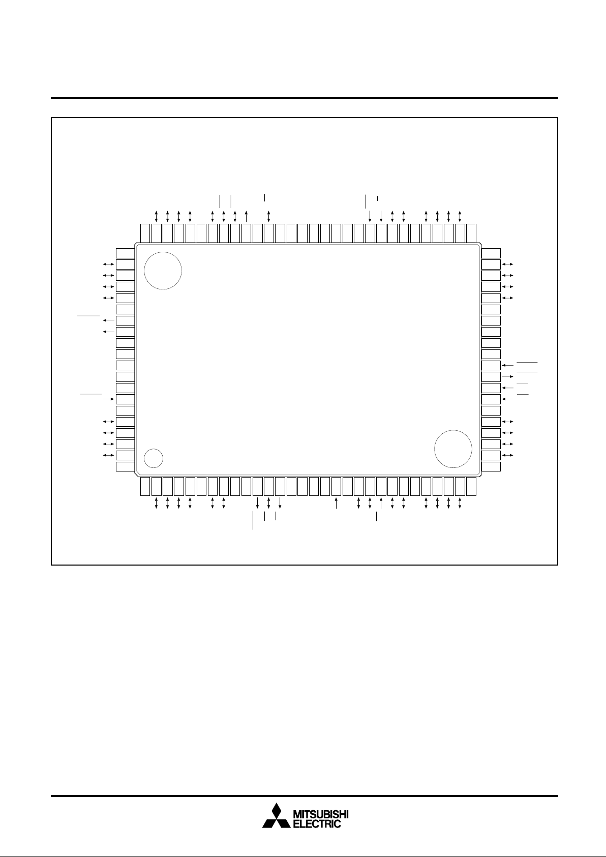
PIN CONFIGURATION (TOP VIEW)
MITSUBISHI MICROCOMPUTERS
M32000D4AFP
SINGLE-CHIP 32-BIT CMOS MICROCOMPUTER
VSS
D15
D14
D13
D12
VCC
BURST
ST
VCC
VSS
VCC
VSS
VCC
WKUP
VCC
D11
D10
D9
D8
VSS
81
82
83
84
85
86
87
88
89
90
91
92
93
94
95
96
97
98
99
100
A28
A29
A30
VCC
80
77
78
79
A27
76
A26
VSS
BCH
73
74
75
VCC
BCL
SID
72
70
71
R/W
69
VCC
VSS
VSS
*1
67
68
VCC
65
66
64
M32000D4AFP
100-pin QFP/0.65 mm pitch
5
4
3
2
1
6
9
8
7
10
13
12
11
16
15
14
17
*1
*1
*1
61
62
63
20
19
18
RST
60
21
M/S
59
22
A25
58
23
A23
VSS
A24
57
55
56
24
26
25
A22
54
27
A20
A21
VCC
51
52
53
50
VSS
49
D7
48
D6
47
D5
46
D4
45
VCC
44
VCC
43
VSS
42
VSS
41
VCC
40
HREQ
HACK
39
SBI
38
INT
37
*1
36
35
D3
34
D2
33
D1
32
D0
31
VSS
30
29
28
A17
A18
A19
VCC
A16
VSS
*1
A14
A15
VCC
BS
DC
STBY
PLLVSS
PLLCAP
PLLVCC
*2
VSS
CLKIN
CS
A13
PP0
PP1
A11
A12
VSS
Note: Connect *1 pins to VCC.
A10
A9
A8
VCC
Connect *2 pins to VSS.
2
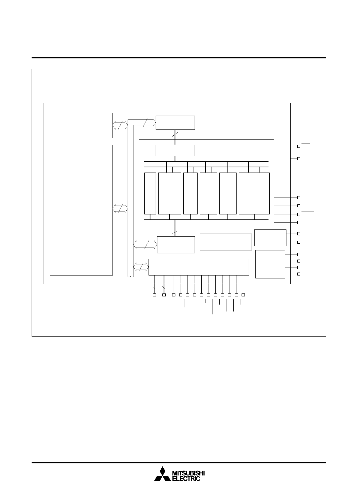
BLOCK DIAGRAM
MITSUBISHI MICROCOMPUTERS
M32000D4AFP
SINGLE-CHIP 32-BIT CMOS MICROCOMPUTER
cache memory
(4K bytes)
DRAM
(2M bytes )
128
128
128
128-bit internal bus
128
128
instru c tio n qu eu e
(128 bits x 2 stages)
instruction decoder
register
32 bits
PC ALU shift
x
16
32 bits
data selector
32 bits
⇔
128 bits
external bus interface unit
32 bits
128 bits
⇔
16 bits
M32R CPU core
load/
store
memory
controller
M32000D4AFP
multiply-
accumulate
unit
32 x 16 bits
MUL
+
56-bit -ACC
programmable
PLL clock
generating
I/O port
circuit
RST
M/S
INT
SBI
WKUP
STBY
PP0
PP1
CLKIN
PLLCAP
PLLVCC
PLLVSS
23
16
ST
BCH
BS
BCL
SID
A8 - A30
D0 - D15
R/W
DC
BURST
HREQ
CS
HACK
3

MITSUBISHI MICROCOMPUTERS
M32000D4AFP
SINGLE-CHIP 32-BIT CMOS MICROCOMPUTER
FUNCTIONS
function block characteristics
CPU core • bus specification
internal DRAM • 16M bits (2M bytes)
cache memory • 4K bytes (internal instruction/data cache mode, instruction cache mode, cache-off mode)
memory controller • cache control
programmable I/O port • two programmable I/O ports
basic bus cycle: 15 ns (internal operation at 66.6 MHz)
logical address space: linear 4G bytes
external address bus: 24 bits (external output pin: A8 to A30, BCH, BCL)
external data bus: 16 bits
• implementation: 5-stage pipeline
• core internal: 32 bits
• register configuration
general-purpose registers: 32 bits ✕ 16
control registers: 32 bits ✕ 5
• instruction set
16-bit/32-bit instruction format
83 instructions/6 addressing modes
• multiply-accumulate operation built in
• internal DRAM control, refresh control
• power management function (standby mode, CPU sleep mode selection control)
____ ____
4
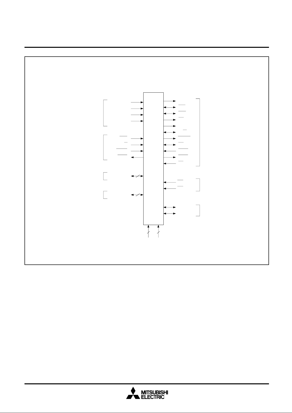
PIN FUNCTION DIAGRAM
MITSUBISHI MICROCOMPUTERS
M32000D4AFP
SINGLE-CHIP 32-BIT CMOS MICROCOMPUTER
clock
system control
address bus
data bus
CLKIN
PLLCAP
PLLVCC
PLLVSS
RST
M/S
WKUP
STBY
A8 - A30
D0 - D15
23
16
M32000D4AFP
16 15
VCC VSS
SID
BCL
BCH
BS
ST
R/W
BURST
DC
HREQ
HACK
CS
INT
SBI
PP0
PP1
bus control
interrupt input
programmable I/O port
5

MITSUBISHI MICROCOMPUTERS
M32000D4AFP
SINGLE-CHIP 32-BIT CMOS MICROCOMPUTER
PIN DESCRIPTION (1/3)
type pin name name I/O function
power VCC power source – All power source pins should be connected to VCC.
source VSS ground – All ground pins should be connected to VSS.
clock CLKIN clock input input Clock input pin. The M32000D4AFP has an internal PLL multiplier
PLLCAP C connection – Connects a capacitor for the internal PLL.
for PLL
PLLVCC power source – Power source for the internal PLL.
for PLL
PLLVSS ground – Ground for the internal PLL.
system
control from standby mode and CPU sleep mode.
____
RST reset input Internally resets the M32000D4AFP. It is also used to return
_
M/S master/slave input Sets the M32000D4AFP default operation to either system bus
______
for PLL
WKUP wakeup input Input pin to request return from standby mode.
_____
STBY standby output Indicates that the M32000D4AFP has switched to standby
address A8 to A30 address bus I/O The M32000D4AFP has a 24-bit address (A8 to A31) bus for
bus (Hi-z)* a 16 MB address space. A31 is not output. During the write
data bus D0 to D15 data bus I/O 16-bit data bus for connecting to external devices.
(Hi-z)*
* (Hi-z): This pin goes to high-impedance in the hold state.
circuit, and an input clock which is 1/4 of the internal operating
frequency (when the internal operating frequency is 66.6 MHz,
the CLKIN input is 16.65 MHz).
master (M/S = "H") or bus slave (M/S = "L").
When the M32000D4AFP is set to bus slave, it does not carry
out a reset vector entry fetch after a reset.
The setting of M/S cannot be changed during operation.
_
Keep at either an "H" or an "L" level.
This is only accepted when STBY is "L" level.
_____
It generates the wakeup interrupt.
mode. An "L" level is output while the device is in standby
mode.
cycle, the valid byte positions on the 16-bit data bus are output
____ ____
as BCH or BCL. During the read cycle, the 16-bit data bus is
read, however,only data in the valid byte positions is transferred
to the M32000D4AFP.
Address bus pins are bidirectional. When accessing the internal
DRAM from an external bus master while the M32000D4AFP is
in the hold state, input the address from the system bus side.
6

MITSUBISHI MICROCOMPUTERS
M32000D4AFP
SINGLE-CHIP 32-BIT CMOS MICROCOMPUTER
PIN DESCRIPTION (2/3)
type pin name name I/O function
bus SID space output Space identifier between user space and I/O space.
control identifier (Hi-z)* SID = "L": user space
____ ____
BCH, BCL byte control I/O Indicates the valid byte positions of transferred data.
(Hi-z)*
__
BS bus start output__When the M32000D4AFP drives an external bus cycle, BS goes
(Hi-z)*
ST bus status output Indicates whether the bus cycle that the M32000D4AFP drives is
(Hi-z)*
__
R/W read/write I/O
(Hi-z)*
______
BURST burst output The M32000D4AFP drives two consecutive bus cycles to access
(Hi-z)*
* (Hi-z): This pin goes to high-impedance in the hold state.
SID = "H": I/O space
SID = undefined: when idle
____ ____
BCH corresponds to the MSB side (D0 to D7), and BCL corresponds
to the LSB side (D8 to D15). During a read bus cycle, both BCH
____
and BCL are an "L" level.
____ ____
During a write bus cycle, either BCH and/or BCL is an "L" level
depending on the byte(s) to be written.
When accessing the internal DRAM from an external bus master,
the byte control signal is input from the system bus side.
to an "L" level at the start of the bus cycle.
__
In burst transfer, BS goes to the "L" level for each transfer
cycle. When accessing internal resources such as an internal
__
DRAM or internal I/O register, BS is not output.
an instruction fetch access cycle or an operand access cycle.
ST = "L": for instruction fetch access
ST = "H": for operand access
ST = undefined: when idle
__
Outputs R/W to identify whether the external bus cycle a read or
a write cycle. When accessing the internal DRAM from an external
__
bus master, R/W is input from the external bus.
32-bit data allocated on the 32-bit word boundary.
For instruction fetches, it drives 8 (max.) consecutive cycles
(8 cycles in instruction cache mode) to data on the 128-bit boundary.
______
During these consecutive bus cycles, BURST goes to "L" level.
When accessing 32-bit data, an "L" level followed by an "H" level
is output from address A30, because the MSB-side 16 bits are
accessed prior to the LSB-side 16 bits.
When accessing 128-bit data, the addresses are output from an
arbitrary 16-bit aligned address and wraparound within a 128-bit
aligned boundary.
____
7

MITSUBISHI MICROCOMPUTERS
SINGLE-CHIP 32-BIT CMOS MICROCOMPUTER
PIN DESCRIPTION (3/3)
type pin name name I/O function
bus
control
(cont.) device in the system bus.
interrupt
controller
programm- PP0, PP1 port I/O Two programmable I/O ports.
able I/O port
__ __
* The DC pin becomes an output pin when the CS signal is input to the M32000D4AFP.
__
DC* data complete I/O When the M32000D4AFP drives an external bus cycle, it
(Hi-z)
automatically inserts wait cycles until DC is input by the slave
When the M32000D4AFP is in the hold state and the internal
DRAM is accessed from an external bus master, the M32000D4AFP
__
outputs DC to notify to the external bus master that the bus
______
HREQ hold input
_____
HACK hold output Indicates that the M32000D4AFP has switched to the hold state
__
acknowledge and releases the bus right of the system bus to the requestor.
cycle to the internal DRAM has been completed.
Bus right request input pin of the system bus. When HREQ is an
"L" level, the M32000D4AFP switches to the hold state.
CS chip input Signal input to the M32000D4AFP when it is in the hold state to
select request access to the internal DRAM from an external bus master.
When an "L"level is input to CS, the M32000D4AFP access
accesses the internal DRAMat the address input via the address
___
pins.
SBI system input System break interrupt input pin. The SBI is not masked by the
break
___
INT external input External interrupt request input pin. It is also used to return from
interrupt
IE bit in the PSW register. It is also used to return from CPU
sleep mode and to request the start of operation in slave mode.
interrupt CPU sleep mode and to request the start of operation the slave
mode.
M32000D4AFP
__
______
__
8

MITSUBISHI MICROCOMPUTERS
M32000D4AFP
SINGLE-CHIP 32-BIT CMOS MICROCOMPUTER
FUNCTIONAL DESCRIPTION
CPU
The M32R CPU has 16 general-purpose registers, 5 control registers, an accumulator and a program counter. The accumulator is of
64-bit width. The registers and program counter are of 32-bit width.
General-purpose registers
The 16 general-purpose registers (R0 - R15) are of 32-bit width and
are used to retain data and base addresses. R14 is used as the link
register and R15 as the stack pointer (SPI or SPU). The link register
is used to store the return address when executing a subroutine call
instruction. The interrupt stack pointer (SPI) and the user stack pointer
(SPU) are alternatively represented by R15 depending on the value
of the stack mode bit (SM) in the processor status word register (PSW).
R0
R1
R2
R3
R4
R5
R6
R7
310
R8
R9
R10
R11
R12
R13
R14 (link register)
R15 (stack pointer)
310
(see note)
Control registers
There are 5 control registers which are the processor status word
register (PSW), the condition bit register (CBR), the interrupt stack
pointer (SPI), the user stack pointer (SPU) and the backup PC (BPC).
The MVTC and MVFC instructions are used for writing and reading
these control registers.
(see notes)
CRn
CR0
CR1
CR2
CR3
CR6
Notes 1: CRn (n = 0 - 3, 6) denotes the control register number.
2: The MVTC and MVFC instructions are used for writing
and reading these control registers.
Fig. 2 Control registers
PSW
CBR
SPI
SPU
BPC
310
processor status word register
condition bit register
interrupt stack pointer
user stack pointer
backup PC
Note: The interrupt stack pointer (SPI) and the user stack pointer (SPU) are
alternatively represented by R15 depending on the value of the stack
mode bit (SM) in the PSW.
Fig. 1 General-purpose registers
9
MITSUBISHI MICROCOMPUTERS
M32000D4AFP
SINGLE-CHIP 32-BIT CMOS MICROCOMPUTER
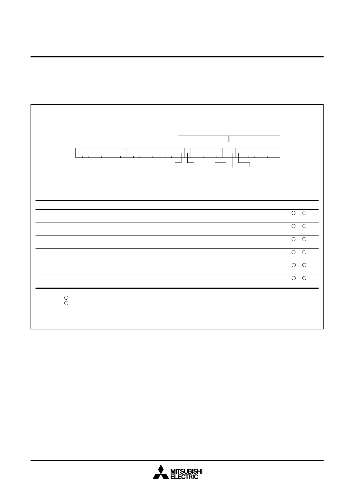
Processor status word register: PSW (CR0)
The processor status word register (PSW) shows the M32R CPU
status. It consists of the current PSW field, and the BPSW field where
a copy of the PSW field is saved when EIT occurs.
The PSW field is made up of the stack mode bit (SM), the interrupt
enable bit (IE) and the condition bit (C). The BPSW field is made up
of the backup stack mode bit (BSM), the backup interrupt enable bit
(BIE) and the backup condition bit (BC).
BPSW field PSW field
16 17 23 24 25 3115870
00000000000000000000000000PSW
SM IE CBCBSM BIE
D bit name function init. R W
16 BSM (backup SM) saves value of SM bit when EIT occurs undefined
17 BIE (backup IE) saves value of IE bit when EIT occurs undefined
23 BC (backup C) saves value of C bit when EIT occurs undefined
24 SM (stack mode) 0: uses R15 as the interrupt stack pointer 0
25 IE (interrupt enable) 0: does not accept interrupt 0
31 C (condition bit) indicates carry, borrow and overflow resulting 0
Note: "init." ...initial state immediately after reset
"R" ....: read enabled
"W" .... : write enabled
Fig. 3 Processor status word register
1: uses R15 as the user stack pointer
1: accepts interrupt
from operations (instruction dependent)
10

MITSUBISHI MICROCOMPUTERS
M32000D4AFP
SINGLE-CHIP 32-BIT CMOS MICROCOMPUTER
Condition bit register
The condition bit register (CBR) is a separate read-only register which
contains a copy of the current value of the condition bit (C) in the
PSW. An attempt to write to the CBR with the MVTC instruction is
ignored.
Interrupt stack pointer, User stack pointer
The interrupt stack pointer (SPI) and the user stack pointer (SPU)
retain the current stack address. The SPI and SPU can be accessed
as the general-purpose register R15. R15 switches between representing the SPI and SPU depending on the value of the stack mode
bit (SM) in the PSW.
SPI
SPU SPU
Backup PC
The backup PC (BPC) is the register where a copy of the PC value is
saved when EIT occurs. Bit 31 is fixed at "0". When EIT occurs, the
PC value immediately before EIT occurrence or that of the next instruction is set. The value of the BPC is reloaded to the PC when the
RTE instruction is executed. However, the values of the lower 2 bits
of the PC become "00" on returning (It always returns to the word
boundary).
310
00000000000000000000000000CBR C00000
310
SPI
310
310
BPCBPC 0
Fig. 4 Condition bit register, interrupt stack pointer, user stack pointer and backup PC
11
MITSUBISHI MICROCOMPUTERS
M32000D4AFP
SINGLE-CHIP 32-BIT CMOS MICROCOMPUTER
Accumulator
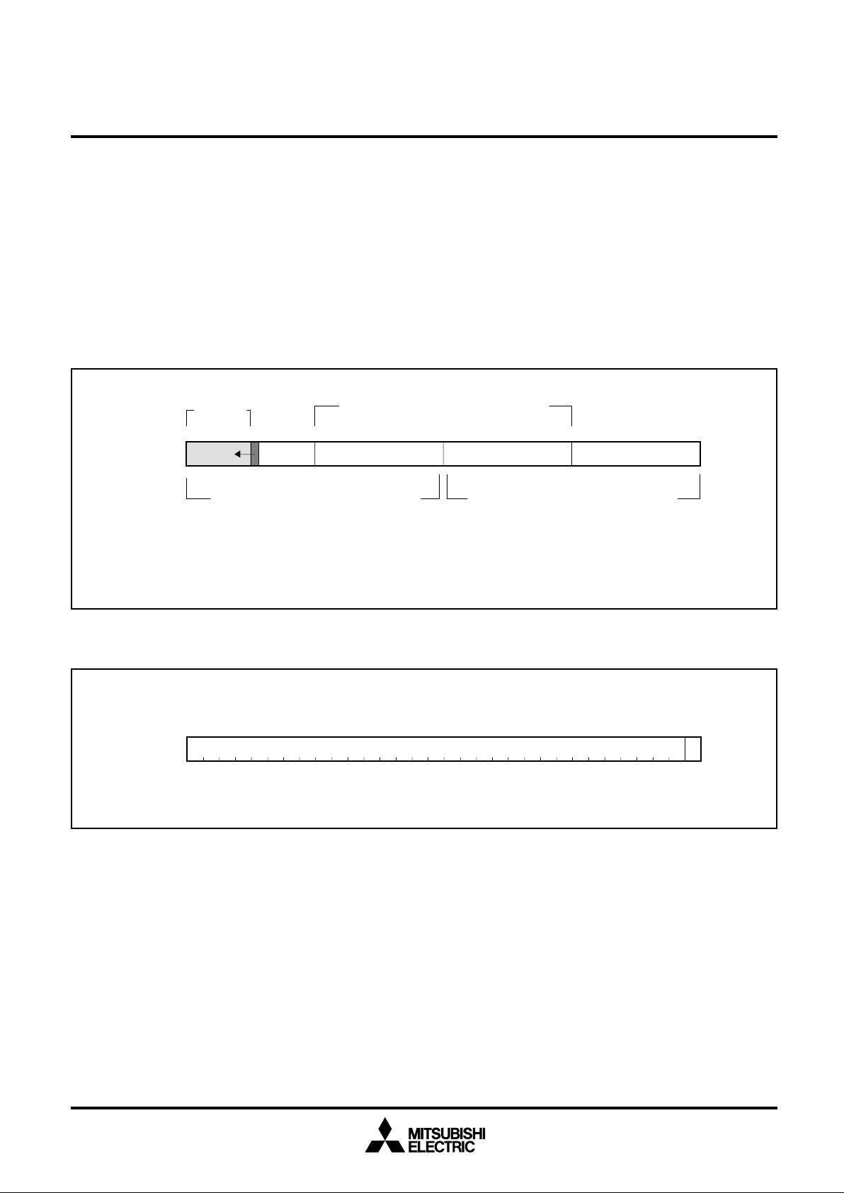
The accumulator (ACC) is a 64-bit register used for DSP type functions. Use the MVTACHI and MVTACLO instructions for writing to
the accumulator. The high-order 32 bits (bit 0 - bit 31) can be set with
the MVTACHI instruction and the low-order 32 bits (bit 32 - bit 63)
can be set with the MVTACLO instruction. Use the MVFACHI,
MVFACLO and MVFACMI instructions for reading from the accumu-
lator. The high-order 32 bits (bit 0 - bit 31) are read with the MVFACHI
instruction, the low order 32 bits (bit 32 - bit 63) with the MVFACLO
instruction and the middle 32 bits (bit 16 - bit 47) with the MVFACMI
instruction.
(see note)
ACC
read/write range with
MVTACHI or MVFACHI instruction
Note: Bits 0 - 7 are always read as the sign-extended value of bit 8.
An attempt to write to this area is ignored.
read range with MVFACMI instruction
Program counter
The program counter (PC) is a 32-bit counter that retains the address of the instruction being executed. Since the M32R CPU instruction starts with even-numbered addresses, the LSB (bit 31) is
always "0".
32 48 633116150 4778
read/write range with
MVTACLO or MVFACLO instruction
Fig. 5 Accumulator
Fig. 6 Program counter
310
PCPC 0
12
MITSUBISHI MICROCOMPUTERS
M32000D4AFP
SINGLE-CHIP 32-BIT CMOS MICROCOMPUTER
Data types
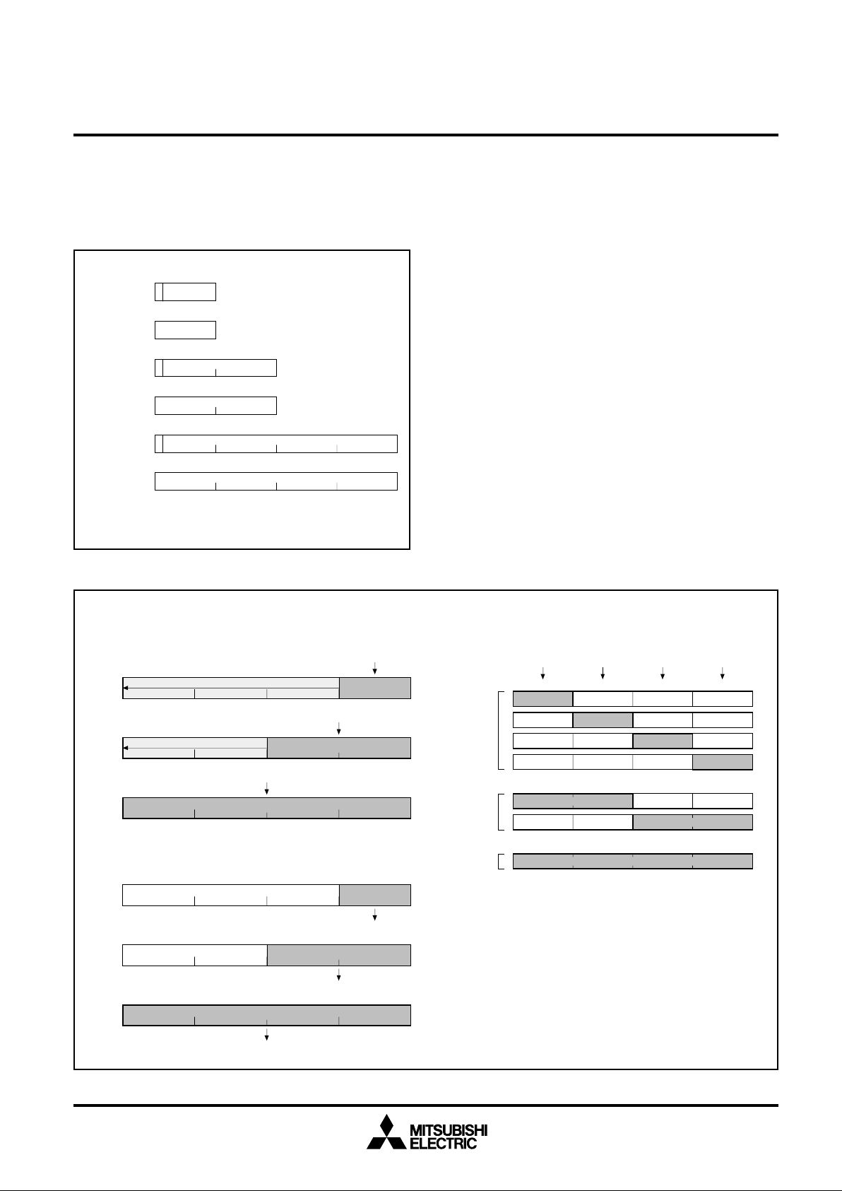
Signed and unsigned integers of byte (8 bits), halfword (16 bits), and
word (32 bits) types are supported as data in the M32R CPU instruction set. A signed integer is represented in a 2's complement format.
signed byte
(8-bit) integer
unsigned byte
(8-bit) integer
signed halfword
(16-bit) integer
unsigned halfword
(16-bit) integer
signed word
(32-bit) integer
unsigned word
(32-bit) integer
Fig. 7 Data type
0
S
0
0
S
0
0
S
0
7
7
15
15
31
31
S: sign bit
Data formats
Data size of a register of the M32R CPU is always a word (32 bits).
Byte (8 bits) and halfword (16 bits) data in memory are sign-extended
(the LDB and LDH instructions) or zero-extended (the LDUB and
LDUH instructions) to 32 bits, and loaded into the register.
Word (32 bits) data in a register is stored to memory by the ST instruction. Halfword (16 bits) data in the LSB side of a register is stored
to memory by the STH instruction. Byte (8 bits) data in the LSB side
of a register is stored to memory by the STB instruction.
Data stored in memory can be one of these types: byte (8 bits),
halfword (16 bits) or word (32 bits).
Although the byte data can be located at any address, the halfword
data and the word data can only be located on the halfword boundary and the word boundary, respectively. If an attempt is made to
access data in memory which is not located on the correct boundary,
an address exception occurs.
<data format in a register>
< load >
Rn
Rn
Rn
< store >
Rn
Rn
Rn
sign-extention (LDB instruction) or
zero-extention (LDUB instruction)
0 31
sign-extention (LDH instruction) or
zero-extention (LDUH instruction)
0 31
from memory (LD instruction)
0 31
0 31
0 31
0 31
from memory (LDH, LDUH instruction)
16
halfword
word
16
halfword
to memory (STH instruction)
word
from memory
(LDB, LDUB instruction)
24
byte
24
byte
to memory (STB instruction)
<data format in memory>
+ 0 + 1 + 2 + 3
0
byte
halfword
word
7 8 15 16 23 24 31
byte
halfword
address
byte
byte
byte
halfword
word
Fig. 8 Data format
to memory (ST instruction)
13

MITSUBISHI MICROCOMPUTERS
M32000D4AFP
SINGLE-CHIP 32-BIT CMOS MICROCOMPUTER
Address space
The M32000D4AFP logical address is 32-bit wide and offers 4 GB
linear space. The M32000D4AFP has address spaces allocated as
shown below.
The user space is specified by SID = 0 (H'0000 0000 to H'7FFF FFFF).
The area available to the user is 16 MB from address H'0000 0000
to address H'00FF FFFF.
The I/O space is specified by SID = 1 (H'8000 0000 to H'FFFF FFFF).
The area available to the user is 16 MB from address H’FF00 0000
to address H'FFFF FFFF. The I/O space cannot be cached.
< logical space >
EIT vector entry
(except for reset interrupt)
logical address
H'0000 0000
(16M bytes)
These areas below are allocated in each space.
• User space
internal DRAM area
external area
• I/O space
user I/O area
system area
internal I/O area
< physical space >
logical address
H'0000 0000
H'001F FFFF
H'0020 0000
internal DRAM
area (2M bytes)
SID
0 : H'00 0000
0 : H'1F FFFF
0 : H'20 0000
physical address
(24 bits)
user space
(SID = 0)
H'7FFF FFFF
H'8000 0000
I/O space
(SID = 1)
H'FFFF FFFF
(16M bytes)
H'00FF FFFF
EIT vector entry
(reset interrupt)
logical address
H'FF00 0000
H'FF7F FFFF
H'FF80 0000
H'FFBF FFFF
H'FFC0 0000
H'FFFF FFFF
external area
(14M bytes)
user I/O area
(8M bytes)
system area
(4M bytes)
internal I/O area
(4M bytes)
0 : H'FF FFFF
physical address
SID
(24 bits)
1 : H'00 0000
1 : H'7F FFFF
1 : H'80 0000
1 : H'BF FFFF
1 : H'C0 0000
1 : H'FF FFFF
Fig. 9 Address space
14
 Loading...