


MITSUBISHI MICROCOMPUTERS
M32000D3FP
SINGLE-CHIP 32-BIT CMOS MICROCOMPUTER
DESCRIPTION
The M32000D3FP is a new generation microcomputer with a 32-bit
CPU and built-in high capacity DRAM. Using this device it is possible
to implement the complex applications of the multimedia age with
high performance and low power consumption.
The M32000D3FP contains 1M bytes of DRAM and 4K bytes of cache
memory. The CPU is implemented with a RISC architecture and has
a high performance figure of 52.4 MIPS (at an internal clock rate of
66.6 MHz ). Memory for main storage is provided internally to the
device eliminating external memory and associated control circuits
thus reducing overall system noise and power consumption.
The CPU, internal DRAM and cache memory are connected by a
128-bit, 15 ns/cycle internal bus which virtually eliminates transfer
bottlenecks in between the CPU and the memory. The M32000D3FP
internally multiplies the frequency of the input clock signals by four.
For an internal operating frequency of 66.6 MHz the input clock frequency is 16.65MHz.
A 16-bit data and 24-bit address bus are the M32000D3FP's external bus and the interface to external peripheral controllers. When the
hold state is set, the internal DRAM can be accessed from an external device.
A 3-chip basic system configuration using the M32000D3FP is the
device itself plus an ASIC as a peripheral controller and a program
ROM. Execution starts from the reset vector entry on the external
ROM after power on, a program requiring high speed execution is
then transferred to internal DRAM and this is then executed. The
M32000D3FP also has a slave mode additional to its master mode.
When set to slave mode the M32000D3FP can be used as a
coprocessor. In this mode it does not access its external bus
immediatly after reset, but waits for the master to start its operation.
FEATURES
CPU ..........................................................M32R family CPU core
•
Pipeline ..............................................................................5 steps
•
Basic bus cycle .................................15 ns (at internal 66.6 MHz)
•
Logical address space ............................................ 4G-byte linear
•
External bus ........................................................ data bus: 16 bits
•
Internal DRAM .................................................8M bits (1M bytes)
•
Cache.......................................................... 4K bytes (direct map)
•
Register configuration...... general-purpose registers: 32 bits x 16
•
Instruction set ....................... 83 instructions/6 addressing modes
•
Instruction format .................................................... 16 bits/32 bits
•
Multiply-accumulate operation unit (DSP function instruction)
•
Internal memory controller
•
Programmable I/O ports
•
Power management function.................................. standby mode
•
PLL clock generating circuit................. four-time clock PLL circuit
•
Operation mode .............................................. master/slave mode
•
Interrupt input............................................................
•
Power source.......................................................... 3.3 V (±10 %)
•
address bus: 24 bits
control registers: 32 bits x 5
/CPU sleep mode
___ ___
INT and SBI
APPLICATIONS
Portable equipment, Still camera, Navigation system,
Digital instrument, Printer, Scanner, FA equipment
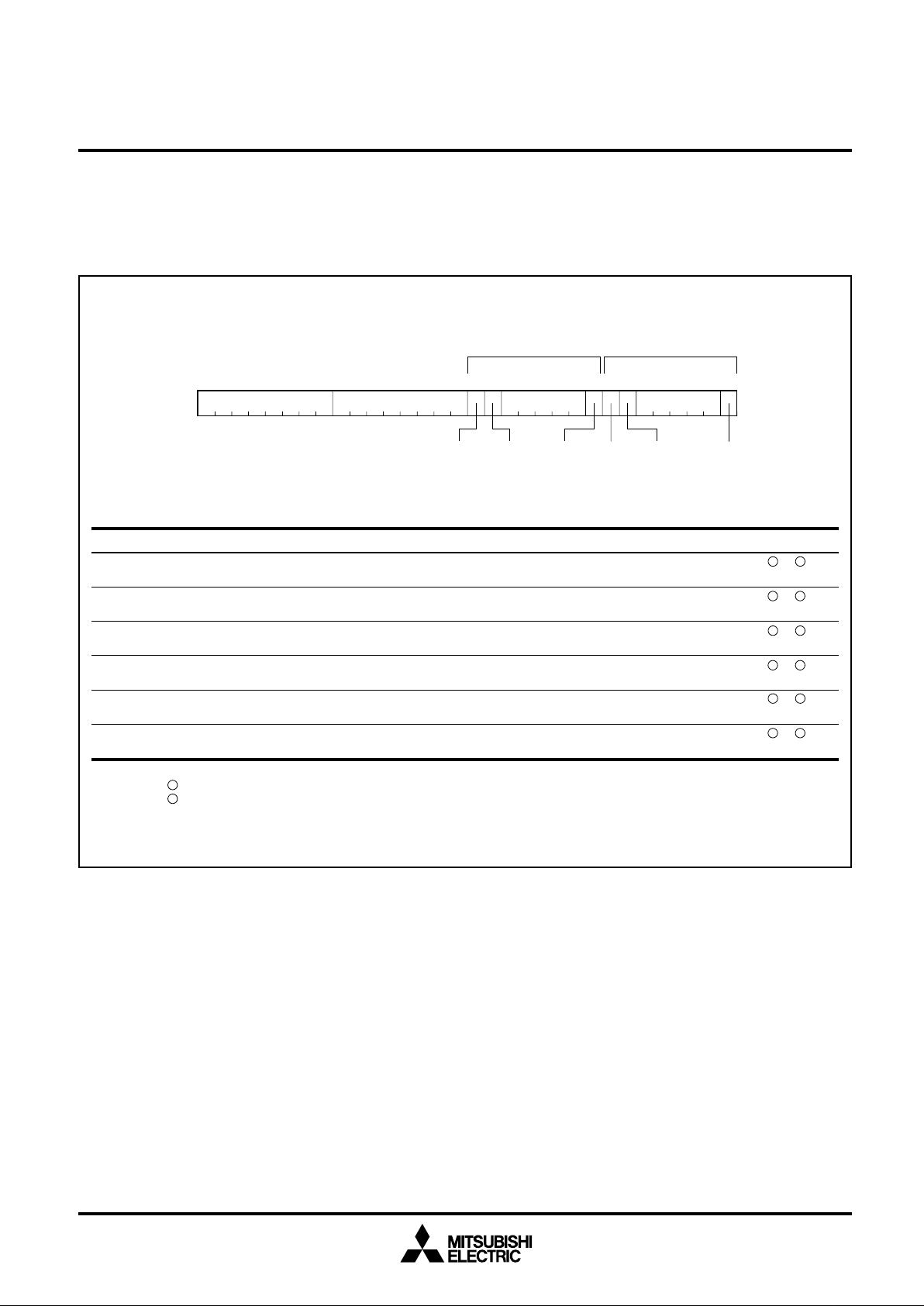
PIN CONFIGURATION (TOP VIEW)
MITSUBISHI MICROCOMPUTERS
M32000D3FP
SINGLE-CHIP 32-BIT CMOS MICROCOMPUTER
VSS
D15
D14
D13
D12
VCC
BURST
ST
VCC
VSS
VCC
VSS
VCC
WKUP
VCC
D11
D10
D9
D8
VSS
81
82
83
84
85
86
87
88
89
90
91
92
93
94
95
96
97
98
99
100
A28
A29
A30
VCC
80
77
78
79
A26
VSS
A27
76
BCH
73
74
75
VCC
BCL
SID
72
70
71
VCC
R/W
*1
68
69
VSS
VSS
VCC
65
66
67
64
M32000D3FP
100-pin QFP/0.65 mm pitch
5
4
3
2
1
6
9
8
7
10
13
12
11
16
15
14
17
*1
*1
*1
61
62
63
20
19
18
A25
M/S
RST
58
59
60
23
22
21
A23
VSS
A24
57
55
56
24
26
25
A22
54
27
A20
A21
VCC
51
52
53
50
49
48
47
46
45
44
43
42
41
40
39
38
37
36
35
34
33
32
31
30
29
28
VSS
D7
D6
D5
D4
VCC
VCC
VSS
VSS
VCC
HREQ
HACK
SBI
INT
*1
D3
D2
D1
D0
VSS
A17
A18
A19
VCC
A16
VSS
*1
A14
A15
VCC
BS
DC
STBY
PLLVSS
PLLCAP
PLLVCC
*2
VSS
CLKIN
CS
A13
PP0
PP1
A11
A12
VSS
A10
A9
A8
VCC
Note: Connect *1 pins to VCC.
Connect *2 pins to VSS.
2
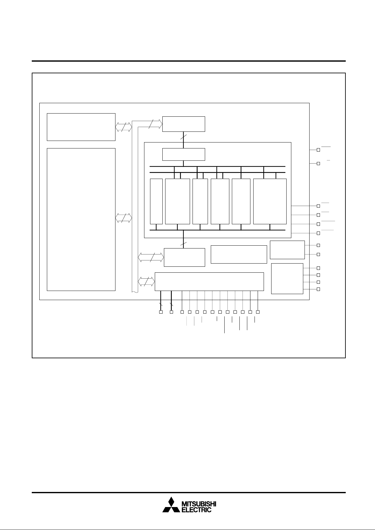
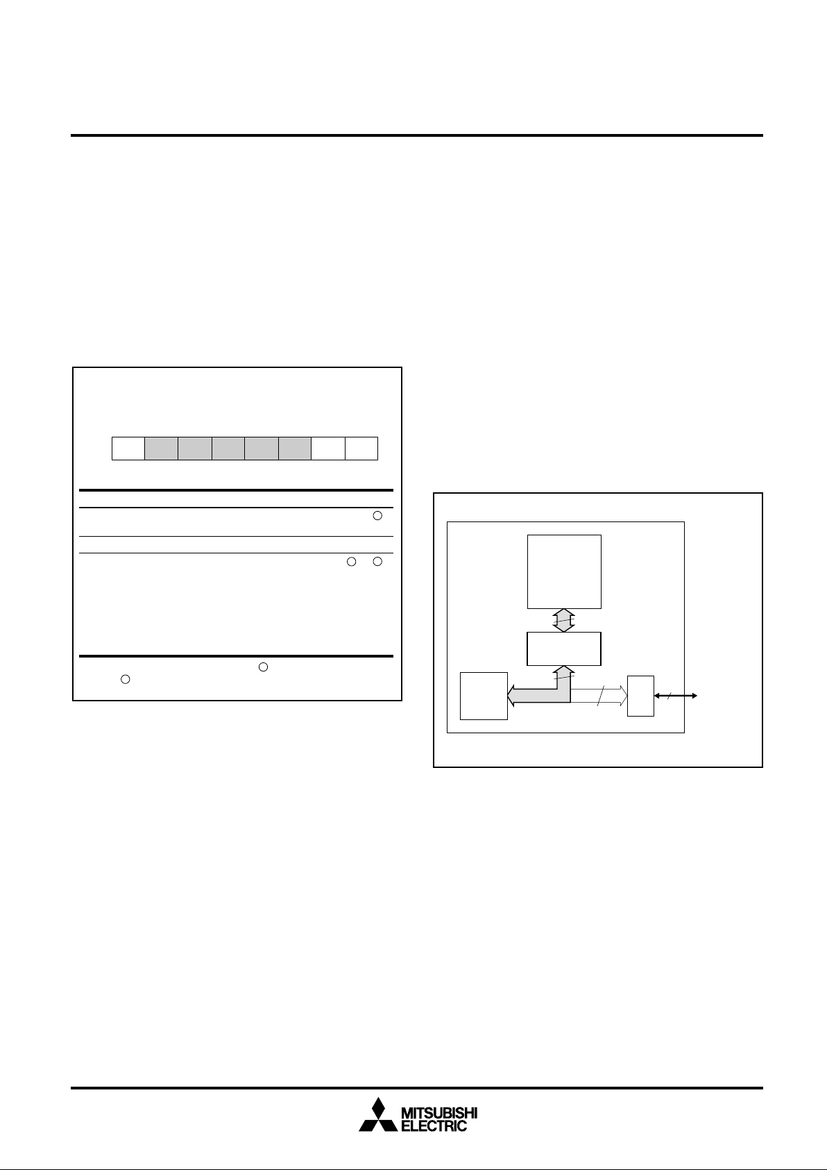
BLOCK DIAGRAM
MITSUBISHI MICROCOMPUTERS
M32000D3FP
SINGLE-CHIP 32-BIT CMOS MICROCOMPUTER
cache memory
(4K bytes)
DRAM
(1M bytes )
128
128
128
128-bit internal bus
128
128
instru c tio n qu eue
(128 bit s x 2 stages)
instruction deco der
register
32 bits
PC ALU shift
x
16
32 bits
data selector
32 bits
⇔
128 bits
external bus interface unit
32 bits
128 bits
⇔
16 bits
M32R CPU core
load/
store
memory
controller
M32000D3FP
multiply-
accumulate
unit
32 x 16 bits
MUL
+
56-bit -ACC
programmable
PLL clock
generating
I/O port
circuit
RST
M/S
INT
SBI
WKUP
STBY
PP0
PP1
CLKIN
PLLCAP
PLLVCC
PLLVSS
23
16
A8 - A30
D0 - D15
BCH
BCL
BS
SID
R/W
DC
BURST
HREQ
CS
HACK
ST
3

MITSUBISHI MICROCOMPUTERS
M32000D3FP
SINGLE-CHIP 32-BIT CMOS MICROCOMPUTER
FUNCTIONS
function block characteristics
CPU core • bus specification
internal DRAM • 8M bits (1M bytes)
cache memory • 4K bytes (internal instruction/data cache mode, instruction cache mode, cache-off mode)
memory controller • cache control
programmable I/O port • two programmable I/O ports
basic bus cycle: 15 ns (internal operation at 66.6 MHz)
logical address space: linear 4G bytes
external address bus: 24 bits (external output pin: A8 to A30, BCH, BCL)
external data bus: 16 bits
• implementation: 5-stage pipeline
• core internal: 32 bits
• register configuration
general-purpose registers: 32 bits ✕ 16
control registers: 32 bits ✕ 5
• instruction set
16-bit/32-bit instruction format
83 instructions/6 addressing modes
• multiply-accumulate operation built in
• internal DRAM control, refresh control
• power management function (standby mode, CPU sleep mode selection control)
____ ____
4
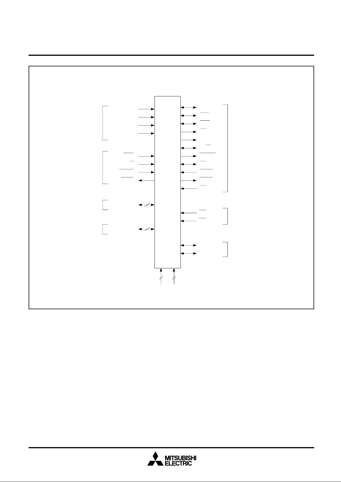
PIN FUNCTION DIAGRAM
MITSUBISHI MICROCOMPUTERS
M32000D3FP
SINGLE-CHIP 32-BIT CMOS MICROCOMPUTER
clock
system control
address bus
data bus
CLKIN
PLLCAP
PLLVCC
PLLVSS
RST
M/S
WKUP
STBY
A8 - A30
D0 - D15
23
16
M32000D3FP
INT
SBI
PP0
PP1
SID
BCL
BCH
BS
ST
R/W
BURST
DC
HREQ
HACK
CS
bus control
interrupt input
programmable I/O port
16 15
VCC VSS
5
MITSUBISHI MICROCOMPUTERS
M32000D3FP
SINGLE-CHIP 32-BIT CMOS MICROCOMPUTER
PIN DESCRIPTION (1/3)
type pin name name I/O function
power VCC power source – All power source pins should be connected to VCC.
source VSS ground – All ground pins should be connected to VSS.
clock CLKIN clock input input Clock input pin. The M32000D3FP has an internal PLL multiplier
PLLCAP C connection – Connects a capacitor for the internal PLL.
for PLL
PLLVCC power source – Power source for the internal PLL.
for PLL
PLLVSS ground – Ground for the internal PLL.
system
control standby mode and CPU sleep mode.
____
RST reset input Internally resets the M32000D3FP. It is also used to return from
_
M/S master/slave input Sets the M32000D3FP default operation to either system bus
______
for PLL
WKUP wakeup input Input pin to request return from standby mode.
_____
STBY standby output Indicates that the M32000D3FP has switched to standby mode.
address A8 to A30 address bus I/O The M32000D3FP has a 24-bit address (A8 to A31) bus for a 16 MB
bus address space. A31 is not output. During the write cycle, the
(Hi-z)*
data bus D0 to D15 data bus I/O 16-bit data bus for connecting to external devices.
(Hi-z)*
* (Hi-z): This pin goes to high-impedance in the hold state.
circuit, and an input clock which is 1/4 of the internal operating
frequency (when the internal operating frequency is 66.6 MHz,
the CLKIN input is 16.65 MHz).
master (M/S = "H") or bus slave (M/S = "L").
When the M32000D3FP is set to bus slave, it does not carry out
a reset vector entry fetch after a reset.
The setting of M/S cannot be changed during operation.
_
Keep at either an "H" or an "L" level.
This is only accepted when STBY is "L" level.
_____
It generates the wakeup interrupt.
An "L" level is output while the device is in standby mode.
valid byte positions on the 16-bit data bus are output as BCH or
____
BCL. During the read cycle, the 16-bit data bus is read, however,
____
only data in the valid byte positions is transferred to the
M32000D3FP.
Address bus pins are bidirectional. When accessing the internal
DRAM from an external bus master while the M32000D3FP is in
the hold state, input the address from the system bus side.
6

MITSUBISHI MICROCOMPUTERS
M32000D3FP
SINGLE-CHIP 32-BIT CMOS MICROCOMPUTER
PIN DESCRIPTION (2/3)
type pin name name I/O function
bus SID space I/O Space identifier between user space and I/O space.
control identifier (Hi-z)* SID = "L": user space
____ ____
BCH, BCL byte control I/O Indicates the valid byte positions of transferred data.
(Hi-z)*
__
BS bus start output__When the M32000D3FP drives an external bus cycle, BS goes
(Hi-z)*
ST bus status output Indicates whether the bus cycle that the M32000D3FP drives is
(Hi-z)*
__
R/W read/write I/O
(Hi-z)*
______
BURST burst output The M32000D3FP drives two consecutive bus cycles to access
(Hi-z)*
* (Hi-z): This pin goes to high-impedance in the hold state.
SID = "H": I/O space
SID is bidirectional. When accessing the internal DRAM from
outside the M32000D3FP while the M32000D3FP is in the hold
state, input an "L" level from the system bus side.
____ ____
BCH corresponds to the MSB side (D0 to D7), and BCL corresponds
to the LSB side (D8 to D15). During a read bus cycle, both BCH
____
and BCL are an "L" level.
____ ____
During a write bus cycle, either BCH and/or BCL is an "L" level
depending on the byte(s) to be written.
When accessing the internal DRAM from an external bus master,
the byte control signal is input from the system bus side.
to an "L" level at the start of the bus cycle.
__
In burst transfer, BS goes to the "L" level for each transfer
cycle. When accessing internal resources such as an internal
__
DRAM or internal I/O register, BS is not output.
an instruction fetch access cycle or an operand access cycle.
ST = "L": for instruction fetch access
ST = "H": for operand access
ST = undefined: when idle
__
Outputs R/W to identify whether the external bus cycle a read or
a write cycle. When accessing the internal DRAM from an external
__
bus master, R/W is input from the external bus.
32-bit data allocated on the 32-bit word boundary.
For instruction fetches, it drives 8 (max.) consecutive cycles
(8 cycles in instruction cache mode) to data on the 128-bit boundary.
______
During these consecutive bus cycles, BURST goes to "L" level.
When accessing 32-bit data, an "L" level followed by an "H" level
is output from address A30, because the MSB-side 16 bits are
accessed prior to the LSB-side 16 bits.
When accessing 128-bit data, the addresses are output from an
arbitrary 16-bit aligned address and wraparound within a 128-bit
aligned boundary.
____
7
MITSUBISHI MICROCOMPUTERS
M32000D3FP
SINGLE-CHIP 32-BIT CMOS MICROCOMPUTER
PIN DESCRIPTION (3/3)
type pin name name I/O function
bus
control
(cont.) device in the system bus.
interrupt
controller break IE bit in the PSW register. It is also used to return from CPU
programm- PP0, PP1 port I/O Two programmable I/O ports.
able I/O port
__ __
* The DC pin becomes an output pin when the CS signal is input to the M32000D3FP.
__
DC* data complete I/O When the M32000D3FP drives an external bus cycle, it
(Hi-z)
automatically inserts wait cycles until DC is input by the slave
__
When the M32000D3FP is in the hold state and the internal
DRAM is accessed from an external bus master, the M32000D3FP
__
outputs DC to notify to the external bus master that the bus
______
HREQ hold input
_____
HACK hold output Indicates that the M32000D3FP has switched to the hold state
__
acknowledge and releases the bus right of the system bus to the requestor.
cycle to the internal DRAM has been completed.
Bus right request input pin of the system bus. When HREQ is an
______
"L" level, the M32000D3FP switches to the hold state.
CS chip input Signal input to the M32000D3FP when it is in the hold state to
select request access to the internal DRAM from an external bus master.
__
When an "L" level is input to CS, the M32000D3FP accesses the
___
SBI system input
___
INT external input External interrupt request input pin. It is also used to return from
interrupt sleep mode and to request the start of operation in slave mode.
internal DRAM at the address input via the address pins.
System break interrupt input pin. The SBI is not masked by the
___
interrupt CPU sleep mode and to request the start of operation the slave
mode.
8
MITSUBISHI MICROCOMPUTERS
M32000D3FP
SINGLE-CHIP 32-BIT CMOS MICROCOMPUTER
FUNCTIONAL DESCRIPTION
CPU
The M32R CPU has 16 general-purpose registers, 5 control registers, an accumulator and a program counter. The accumulator is of
64-bit width. The registers and program counter are of 32-bit width.
General-purpose registers
The 16 general-purpose registers (R0 - R15) are of 32-bit width and
are used to retain data and base addresses. R14 is used as the link
register and R15 as the stack pointer (SPI or SPU). The link register
is used to store the return address when executing a subroutine call
instruction. The interrupt stack pointer (SPI) and the user stack pointer
(SPU) are alternatively represented by R15 depending on the value
of the stack mode bit (SM) in the processor status word register (PSW).
R0
R1
R2
R3
R4
R5
R6
R7
310
R8
R9
R10
R11
R12
R13
R14 (link register)
R15 (stack pointer)
310
(see note)
Control registers
There are 5 control registers which are the processor status word
register (PSW), the condition bit register (CBR), the interrupt stack
pointer (SPI), the user stack pointer (SPU) and the backup PC (BPC).
The MVTC and MVFC instructions are used for writing and reading
these control registers.
(see notes)
CRn
CR0
CR1
CR2
CR3
CR6
Notes 1: CRn (n = 0 - 3, 6) denotes the control register number.
2: The MVTC and MVFC instructions are used for writing
and reading these control registers.
Fig. 2 Control registers
PSW
CBR
SPI
SPU
BPC
310
processor status word register
condition bit register
interrupt stack pointer
user stack pointer
backup PC
Note: The interrupt stack pointer (SPI) and the user stack pointer (SPU) are
alternatively represented by R15 depending on the value of the stack
mode bit (SM) in the PSW.
Fig. 1 General-purpose registers
9
MITSUBISHI MICROCOMPUTERS
M32000D3FP
SINGLE-CHIP 32-BIT CMOS MICROCOMPUTER
Processor status word register: PSW (CR0)
The processor status word register (PSW) shows the M32R CPU
status. It consists of the current PSW field, and the BPSW field where
a copy of the PSW field is saved when EIT occurs.
The PSW field is made up of the stack mode bit (SM), the interrupt
enable bit (IE) and the condition bit (C). The BPSW field is made up
of the backup stack mode bit (BSM), the backup interrupt enable bit
(BIE) and the backup condition bit (BC).
BPSW field PSW field
16 17 23 24 25 3115870
00000000000000000000000000PSW
SM IE CBCBSM BIE
D bit name function init. R W
16 BSM (backup SM) saves value of SM bit when EIT occurs undefined
17 BIE (backup IE) saves value of IE bit when EIT occurs undefined
23 BC (backup C) saves value of C bit when EIT occurs undefined
24 SM (stack mode) 0: uses R15 as the interrupt stack pointer 0
25 IE (interrupt enable) 0: does not accept interrupt 0
31 C (condition bit) indicates carry, borrow and overflow resulting 0
Note: "init." ...initial state immediately after reset
"R" .... : read enabled
"W" .... : write enabled
Fig. 3 Processor status word register
1: uses R15 as the user stack pointer
1: accepts interrupt
from operations (instruction dependent)
10
MITSUBISHI MICROCOMPUTERS
M32000D3FP
SINGLE-CHIP 32-BIT CMOS MICROCOMPUTER
Condition bit register
The condition bit register (CBR) is a separate read-only register which
contains a copy of the current the condition bit (C) in the PSW. This
register is read-only. An attempt to write to the CBR with the MVTC
instruction is ignored.
Interrupt stack pointer, User stack pointer
The interrupt stack pointer (SPI) and the user stack pointer (SPU)
retain the current stack address. The SPI and SPU can be accessed
as the general-purpose register R15. R15 switches between representing the SPI and SPU depending on the value of the stack mode
bit (SM) in the PSW.
SPI
SPU SPU
Backup PC
The backup PC (BPC) is the register where a copy of the PC value is
saved when EIT occurs. Bit 31 is fixed at "0". When EIT occurs, the
PC value immediately before EIT occurrence or that of the next instruction is set. The value of the BPC is reloaded to the PC when the
RTE instruction is executed. However, the values of the lower 2 bits
of the PC become "00" on returning (It always returns to the word
boundary).
310
00000000000000000000000000CBR C00000
310
SPI
310
310
BPCBPC 0
Fig. 4 Condition bit register, interrupt stack pointer, user stack pointer and backup PC
11
MITSUBISHI MICROCOMPUTERS
M32000D3FP
SINGLE-CHIP 32-BIT CMOS MICROCOMPUTER
Accumulator
The accumulator (ACC) is a 64-bit register used for DSP type functions. Use the MVTACHI and MVTACLO instructions for writing to
the accumulator. The high-order 32 bits (bit 0 - bit 31) can be set with
the MVTACHI instruction and the low-order 32 bits (bit 32 - bit 63)
can be set with the MVTACLO instruction. Use the MVFACHI,
MVFACLO and MVFACMI instructions for reading from the accumu-
lator. The high-order 32 bits (bit 0 - bit 31) are read with the MVFACHI
instruction, the low order 32 bits (bit 32 - bit 63) with the MVFACLO
instruction and the middle 32 bits (bit 16 - bit 47) with the MVFACMI
instruction.
(see note)
ACC
read/write range with
MVTACHI or MVFACHI instruction
Note: Bits 0 - 7 are always read as the sign-extended value of bit 8.
An attempt to write to this area is ignored.
read range with MVFACMI instruction
Program counter
The program counter (PC) is a 32-bit counter that retains the address of the instruction being executed. Since the M32R CPU instruction starts with even-numbered addresses, the LSB (bit 31) is
always "0".
32 48 633116150 4778
read/write range with
MVTACLO or MVFACLO instruction
Fig. 5 Accumulator
Fig. 6 Program counter
310
PCPC 0
12
MITSUBISHI MICROCOMPUTERS
M32000D3FP
SINGLE-CHIP 32-BIT CMOS MICROCOMPUTER
Data types
Signed and unsigned integers of byte (8 bits), halfword (16 bits), and
word (32 bits) types are supported as data in the M32R CPU instruction set. A signed integer is represented in a 2's complement format.
signed byte
(8-bit) integer
unsigned byte
(8-bit) integer
signed halfword
(16-bit) integer
unsigned halfword
(16-bit) integer
signed word
(32-bit) integer
unsigned word
(32-bit) integer
Fig. 7 Data type
0
S
0
0
S
0
0
S
0
7
7
15
15
31
31
S: sign bit
Data formats
Data size of a register of the M32R CPU is always a word (32 bits).
Byte (8 bits) and halfword (16 bits) data in memory are sign-extended
(the LDB and LDH instructions) or zero-extended (the LDUB and
LDUH instructions) to 32 bits, and loaded into the register.
Word (32 bits) data in a register is stored to memory by the ST instruction. Halfword (16 bits) data in the LSB side of a register is stored
to memory by the STH instruction. Byte (8 bits) data in the LSB side
of a register is stored to memory by the STB instruction.
Data stored in memory can be one of these types: byte (8 bits),
halfword (16 bits) or word (32 bits).
Although the byte data can be located at any address, the halfword
data and the word data can only be located on the halfword boundary and the word boundary, respectively. If an attempt is made to
access data in memory which is not located on the correct boundary,
an address exception occurs.
<data format in a register>
< load >
Rn
Rn
Rn
< store >
Rn
Rn
Rn
sign-extention (LDB instruction) or
zero-extention (LDUB instruction)
0 31
sign-extention (LDH instruction) or
zero-extention (LDUH instruction)
0 31
from memory (LD instruction)
0 31
0 31
0 31
0 31
from memory (LDH, LDUH instruction)
16
halfword
word
16
halfword
to memory (STH instruction)
word
from memory
(LDB, LDUB instruction)
24
byte
24
byte
to memory (STB instruction)
<data format in memory>
+ 0 + 1 + 2 + 3
7 8
870
byte
byte
halfword
word
halfword
byte
address
15
16 23 24
byte
word
311615
byte
halfword
Fig. 8 Data format
to memory (ST instruction)
13
MITSUBISHI MICROCOMPUTERS
M32000D3FP
SINGLE-CHIP 32-BIT CMOS MICROCOMPUTER
Address space
The M32000D3FP logical address is 32-bit wide and offers 4 GB
linear space. The M32000D3FP has address spaces allocated as
shown below.
The user space is specified by SID = 0 (H'0000 0000 to H'7FFF FFFF).
The area available to the user is 16 MB from address H'0000 0000
to address H'00FF FFFF.
The I/O space is specified by SID = 1 (H'8000 0000 to H'FFFF FFFF).
The area available to the user is 16 MB from address H’FF00 0000
to address H'FFFF FFFF. The I/O space cannot be cached.
< logical space >
EIT vector entry
(except for reset interrupt)
logical address
H'0000 0000
(16M bytes)
These areas below are allocated in each space.
• User space
internal DRAM area
external area
• I/O space
user I/O area
system area
internal I/O area
< physical space >
logical address
H'0000 0000
H'000F FFFF
H'0010 0000
internal DRAM
area (1M bytes)
SID
0 : H'00 0000
0 : H'0F FFFF
0 : H'10 0000
physical address
(24 bits)
user space
(SID = 0)
H'7FFF FFFF
H'8000 0000
I/O space
(SID = 1)
H'FFFF FFFF
(16M bytes)
H'00FF FFFF
EIT vector entry
(reset interrupt)
logical address
H'FF00 0000
H'FF7F FFFF
H'FF80 0000
H'FFBF FFFF
H'FFC0 0000
H'FFFF FFFF
external area
(15M bytes)
user I/O area
(8M bytes)
system area
(4M bytes)
internal I/O area
(4M bytes)
0 : H'FF FFFF
physical address
SID
(24 bits)
1 : H'00 0000
1 : H'7F FFFF
1 : H'80 0000
1 : H'BF FFFF
1 : H'C0 0000
1 : H'FF FFFF
Fig. 9 Address space
14

MITSUBISHI MICROCOMPUTERS
M32000D3FP
SINGLE-CHIP 32-BIT CMOS MICROCOMPUTER
The internal DRAM (1 MB) is allocated from address H'0000 0000 to
address H'000F FFFF. The EIT vector entry (other than the reset
interrupt) is allocated in the address H'0000 0000 to address H'0000
008F of this area.
The internal DRAM is connected to the M32R CPU via a 4 KB cache
memory with a 128-bit bus. When the M32000D3FP is in the hold
state, the internal DRAM can be accessed from an external bus master
by inputting control signals.
The external area consists of 15 MB from address H'0010 0000 to
address H'00FF FFFF. When this space is accessed, the control signals to access external devices are output. The bottom 16 bytes in
this area (H'00FF FFF0 to H'00FF FFFF) are the reset interrupt EIT
vector entry.
logical address
0
H'FFC0 0000
(reserved)
H'FFFF FFE0
H'FFFF FFE4
H'FFFF FFE8
H'FFFF FFEC
The user I/O area is 8 MB from address H'FF00 0000 to address
H'FF7F FFFF. When this space is accessed, the control signals to
access external devices are output. The system area is 4 MB from
address H'FF80 0000 to address H'FFBF FFFF. This area is reserved
for development tools such as in-circuit emulators or debug monitors. The user cannot use this area.
The internal I/O area is 4 MB from address H'FFC0 0000 to address
H'FFFF FFFF. The memory controller and programmable I/O port
registers are allocated in this area.
+2 address+1 address+0 address
+3 address
PPCR0
PPCR1
PPDR0
PPDR1
31
programmable I/O port
H'FFFF FFF4
H'FFFF FFF8
H'FFFF FFFC
PPCR0: programmable I/O port direction control register 0
PPCR1: programmable I/O port direction control register 1
PPDR0: programmable port data register 0
PPDR1: programmable port data register 1
Fig. 10 Internal I/O space memory map
(reserved)
MLCR
MPMR
MCCR
MLCR: lock control register
MPMR: power management control register
MCCR: cache control register
memory controller
15

MITSUBISHI MICROCOMPUTERS
M32000D3FP
SINGLE-CHIP 32-BIT CMOS MICROCOMPUTER
EIT
While the CPU is executing a program, sometimes it is necessary to
suspend execution, because a certain event occurs, and execute
another program. These kinds of events are referred to as EIT (Exception, Interrupt, Trap).
• Exception
The event is related to the context being executed. It is generated by
errors or violations that occur during instruction execution. With the
M32000D3FP, the address exception (AE) and reserved instruction
exception (RIE) are of this type.
• Interrupt
The event is not related to the context being executed. It is generated by an external hardware signal. With the M32000D3FP, the
external interrupt (EI), system break interrupt (SBI), wakeup interrupt (WI) and reset interrupt (RI) are of this type.
• Trap
This is a software interrupt which is generated by executing the TRAP
instruction. It is intentionally added to the program by the programmer, as a system call.
EIT
Exception Reserved Instruction
Interrupt Reset Interrupt (RI)
Exception (RIE)
Address Exception (AE)
Wakeup Interrupt (WI)
System Break Interrupt (SBI)
External Interrupt (EI)
EIT events are shown below.
• Reserved instruction exception (RIE)
The reserved instruction exception (RIE) occurs when execution of a
reserved instruction (unimplemented instruction) is detected.
• Address exception (AE)
The address exception (AE) occurs if an attempt is made to access
an unaligned address with either a load instruction or a store instruction.
• Reset interrupt (RI)
The reset interrupt (RI) is always accepted when the RST signal is
___
input. It has the highest priority.
• Wakeup interrupt (WI)
The wakeup interrupt (WI) is accepted when the WKUP signal is
______
input while the M32000D3FP is in standby mode. It is only used to
return from standby mode.
• System break interrupt (SBI)
The system break interrupt (SBI) is an interrupt request from the SBI
___
pin. It is used when a break in power source or an error from an
external watchdog timer is detected. It is also used to return from
CPU sleep mode and to start an M32000D3FP set to slave mode.
• External interrupt (EI)
The external interrupt (EI) is an interrupt request from the INT pin. It
___
is used by an interrupt from the external peripheral I/O and can be
masked by the IE bit in the PSW register. It is also used to return
from CPU sleep mode and to start an M32000D3FP set to slave
mode.
• Trap
The trap (TRAP) is a software interrupt which is generated by executing the TRAP instruction. A total of 16 EIT vector entries are
available for operands 0 to 15 of the TRAP instruction.
Trap
Fig. 11 EIT events
Trap (TRAP)
16
MITSUBISHI MICROCOMPUTERS
M32000D3FP
SINGLE-CHIP 32-BIT CMOS MICROCOMPUTER
Internal memory system
The memory system built into the M32000D3FP has the following
characteristics.
• internal 8M-bit (1M-byte) DRAM
• internal 4K-byte cache memory
• CPU, cache and internal DRAM are connected by a 128-bit bus
• selectable cache memory operation mode
– internal instruction/data cache mode
– instruction cache mode
– cache-off mode
cache control register (MCCR) < address: H'FFFF FFFF>
D24 D25 D26 D27 D28 D29 D30 D31
CP
D bit name function R W
24 CP 0: no purge 0
(cache purge) 1: purge
25 - 29 Not assigned. 0
30, 31 CM0, CM1 00: cache mode
(cache mode) is not changed
01: cache-off mode
10: internal
instruction/data
cache mode
11: instruction cache
mode
R = 0 ... "0" when reading R = ... read enabled
W = ... write enabled W = : write disabled
✕
Fig. 12 Cache control register
CM0 CM1
<at reset: H'01>
✕
When the internal instruction/data cache mode is selected, the cache
memory functions as a cache for both instruction and data from the
internal DRAM, and caches all bus access to the DRAM. This mode
is for a system which uses the internal DRAM as main memory. Transfer between the M32R CPU, cache memory and internal DRAM is
always carried out in blocks of 128 bits. Caching is carried out by the
direct map method. Writing is by the copy back method.
When the M32000D3FP access destination is an external space,
data transfer between the M32R CPU and the external device is carried out via the bus interface unit (BIU). The BIU has a 128-bit data
buffer which converts the bus width between the 128-bit bus in the
M32000D3FP and the external bus. Caching is not applicable in this
case of data transfer.
When accessing the internal DRAM from an external bus master,
and a cache hit occurs (the accessed data is inside the cache), data
transfer between the cache memory and the external bus via the BIU
is carried out. When a cache miss occurs, (the accessed data is not
inside the cache) data transfer is carried out between the internal
DRAM and the external bus via the BIU without cache replacement.
M32000D3FP
DRAM
128
CPU
instruction/
data cache
128
128
external bus
interface
BIU
16
external bus
(16 bits)
Fig. 13 Internal instruction/data cache mode
17

MITSUBISHI MICROCOMPUTERS
M32000D3FP
SINGLE-CHIP 32-BIT CMOS MICROCOMPUTER
When the instruction cache mode is selected, the cache functions as
an instruction cache for the internal DRAM or the external memory,
and caching is carried out for instruction fetch access. This mode is
designed for use when an external ROM is used as program memory
and the internal DRAM is used as data memory, or when instructions
are located in the internal DRAM. Caching is carried out by the direct
map method. When instruction codes in the user space are overwritten by the external bus master or another source, instruction code
coherency in the cache memory is not guaranteed. Furthermore,
caching is not applied when accessing the internal DRAM from the
external bus master.
M32000D3FP
DRAM
external bus
interface
BIU
16
external bus
(16 bits)
CPU
128
instruction
cache
128
When the cache-off mode is selected, the M32000D3FP internal
memory system is configured as follows. In this mode, caching is not
applied, and all bus cycles are directly to the internal DRAM or external bus.
M32000D3FP
DRAM
external bus
interface
128
CPU
128
BIU
16
external bus
(16 bits)
Fig. 15 Cache-off mode
Fig. 14 Instruction cache mode
18

MITSUBISHI MICROCOMPUTERS
M32000D3FP
SINGLE-CHIP 32-BIT CMOS MICROCOMPUTER
Bus interface unit (BIU)
The M32000D3FP has the following signals related to the external
bus.
• Address (A8 to A30)
The M32000D3FP has a 24-bit address bus (A8 to A31) corresponding to a 16 MB address space. Of these, A31 (the LSB) is not output
externally. In write cycles, the validity of the two bytes output on the
16-bit data bus is indicated by BCH and/or BCL. In read cycles, the
16-bit data bus is always read, however, only data in the valid byte
position in the M32000D3FP is transferred. The address pins are
bidirectional. If the M32000D3FP is in the hold state and the internal
DRAM is accessed from an external bus master, the address signal
is input from the system bus side.
• Space identifier (SID)
The space identifier is used to specify user space and I/O space.
user space: SID = "L"
I/O space: SID = "H"
If the M32000D3FP is in the hold state and the internal DRAM is
accessed from an external bus master, the "L" level should be input
to SID from the system bus side.
___ ___
• Byte control (BCH, BCL)
Byte control signals indicate the byte position of valid data transferred of the external bus cycle. BCH corresponds to the MSB side
________
(D0 to D7), and BCL corresponds to the LSB side (D8 to D15). During the bus read cycle, both BCH and BCL are an "L" level. During
___ ___
the bus write cycle, BCH and/or BCL go to an "L" level depending on
the bytes to be written. If the M32000D3FP is in the hold state and
the internal DRAM is accessed from an external bus master, the byte
control signal is input from the system bus side.
• Data bus (D0 to D15)
The M32000D3FP has a 16-bit data bus to access external devices.
If the M32000D3FP is in the hold state and the internal DRAM is
accessed from an external bus master, the data bus is used as a
data I/O bus from the system bus side.
__
• Bus start (BS)
When the M32000D3FP drives the bus cycle to the system bus, an
"L" level is output to BS at the start of the bus cycle. Also, for a burst
__
__ __
transfer, the BS signal is output for each transfer cycle. The BS signal is not output when accessing internal resources such as the internal DRAM or internal I/O registers.
___ ___
___
___ ___
• Bus status (ST)
The ST signal identifies whether the bus cycle the M32000D3FP is
driving is an instruction fetch cycle or an operand access cycle.
instruction fetch access: ST = "L"
operand access: ST = "H"
hold: ST = high-impedance
idle: ST = undefined
• Read/write (R/W)
__
__
The M32000D3FP outputs a R/W signal to identify whether the external bus cycle is a read or write operation. When accessing the
__
internal DRAM from an external bus master, a R/W signal is input
from the system bus side.
read bus cycle: R/W = "H"
write bus cycle: R/W = "L"
______
__
__
• Burst (BURST)
The M32000D3FP drives two consecutive bus cycles to access 32bit data located on the 32-bit boundary. In instruction fetching, it drives
a maximum of 8 (fixed to 8 cycles in instruction cache mode) consecutive read cycles to access data located on the 128-bit boundary.
While driving these consecutive bus cycles, the M32000D3FP out-
______
puts "L" level to BURST. When accessing 32-bit data, the address of
the MSB-side 16 bits are output before the address of the LSB side
16 bits. When accessing 128-bit data, the addresses are output for
every access cycle from the arbitrary 16-bit aligned addresses to
wraparound within the 128-bit boundary.
__
• Data complete (DC)
When starting an external bus cycle, the M32000D3FP automatically inserts wait cycles until the DC signal is input from external.
__
__
Wait control using the DC signal is effective also for bus cycles during burst transfer. When the M32000D3FP is in the hold state and if
__ __
the CS signal is input, the M32000D3FP outputs the DC signal to
notify the external bus master that internal DRAM access is complete.
_____ _____
• Hold control (HREQ, HACK)
The hold state is the state when the external bus access stops and
all pins go to a high-impedance state. However, the internal DRAM
can be accessed while the external bus is in the hold state. To put
_____
the M32000D3FP into the hold state, input an "L" level to HREQ.
When the hold request is accepted and the M32000D3FP enters the
_____
hold state, an "L" level is output from HACK.
19

MITSUBISHI MICROCOMPUTERS
M32000D3FP
SINGLE-CHIP 32-BIT CMOS MICROCOMPUTER
• Internal DRAM access control (CS)
The internal DRAM can be accessed when CS is driven to an "L"
__
__
____
level after the M32000D3FP enters the hold state (HACK = "L").
To access the internal DRAM from external, the following signals
from the system bus side should be controlled.
• A8 to A30
Input internal DRAM addresses to be read or written.
___
___
• BCH, BCL
Specify the byte position of data to be written into the internal
___ ___
DRAM. BCH corresponds to the MSB side (D0 to D7), and BCL
corresponds to the LSB side (D8 to D15).
__
• R/W
Specify read or write operation. When reading, R/W = "H". When
__
___
writing, R/W = "L".
• D0 to D15
16-bit data I/O bus.
• SID
When accessing the internal DRAM from an external bus master, an "L" level is input to SID to specify user space.
_____
• DC
This signal notifies to an external bus master that the internal
DRAM access is complete. When access is complete, an "L"
_____
level is output to DC.
Table 1 Pin condition in hold state
pin name pin condition or operation
A8 - A30, SID, high-impedance
____ ____
BCH, BCL
__ ___ ______
ST, R/W, BS, BURST
D0 - D15 output when internal DRAM is read
by an external bus master (CS = "L",
__
__
R/W = "H"), otherwise high-impedance
__
DC output when internal DRAM is
accessed by an external bus master
__
_____
(CS = "L"), otherwise high-impedance
HACK output "L"
other pins normal operation
Read and write operations of the M32000D3FP are carried out using
the address bus, data bus, and the R/W, BCH, BCL and DC signals.
When reading, the R/W signal goes to an "H" level, and the BCH and
_______
___ _______
BCL signals go to an "L" level. The CPU reads the data in the valid
byte positions. When writing, an "L" level is output from R/W, and
_______ _______
___ _______ _______ _____
___
BCH and BCL are output according to the valid byte positions, so as
to specify the byte positions for writing into an external device.
CLKIN
BS
A8 - A30
SID, ST
R/W
BCH, BCL
BURST
D0 - D15
DC
CLKIN
BS
A8 - A30
SID, ST
idle read
"H"
"H"
"Hi-z" "Hi-z"
idle write idlewrite
idleread
20
R/W
BCH, BCL
BURST
D0 - D15
"H"
"Hi-z" "Hi-z"
DC
Note: "Hi-z" means high-impedance, and indicates sampling timing.
Keep DC signal at the "H" level during idle cycles.
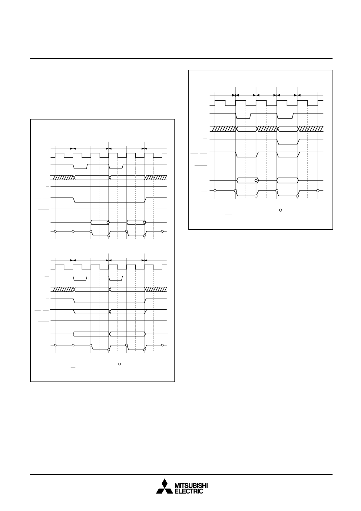
Fig. 16 Read/write timing (two no-wait accesses)
MITSUBISHI MICROCOMPUTERS
M32000D3FP
SINGLE-CHIP 32-BIT CMOS MICROCOMPUTER
When an "L" level is input to DC, the next bus cycle is processed and
wait cycles are inserted until this point. Keep the DC signal at the "H"
__
__
level, unless otherwise necessary. When a write cycle comes immediately after a read cycle, the M32000D3FP inserts an idle cycle to
prevent a collision with data on the system bus. The same applies to
write cycles (burst write access) immediately after a burst read cycle.
CLKIN
A8 - A30
SID, ST
R/W
BCH, BCL
BURST
D0 - D15
idle read
BS
"H"
"H"
"Hi-z" "Hi-z" "Hi-z"
DC
idleread
CLKIN
BS
A8 - A30
SID, ST
R/W
BCH, BCL
BURST
D0 - D15
DC
idle
"H"
"Hi-z" "Hi-z" "Hi-z"
idleread write idle
Note: "Hi-z" means high-impedance, and indicates sampling timing.
Keep DC signal at the "H" level during idle cycles.
Fig. 18 Automatic idle cycle insertion between consecutive read
and write cycles
idle write idlewrite
CLKIN
BS
A8 - A30
SID, ST
R/W
BCH, BCL
BURST
"H"
D0 - D15
"Hi-z" "Hi-z"
DC
Note: "Hi-z" means high-impedance, and indicates sampling timing.
Keep DC signal at the "H" level during idle cycles.
Fig. 17 Read/write timing (two one-wait accesses)
21

MITSUBISHI MICROCOMPUTERS
M32000D3FP
SINGLE-CHIP 32-BIT CMOS MICROCOMPUTER
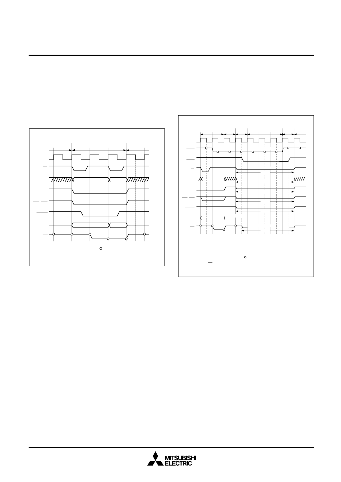
The M32000D3FP outputs the BURST signal and carries out a burst
______
transfer when reading "the word-size data aligned on the 32-bit boundary" or "a maximum 4 words of instructions aligned on the 128-bit
boundary". The BURST signal is synchronized with the CLKIN falling
______
edge of the first bus access cycle and output "L" level. It returns to an
"H" level synchronized with the first CLKIN falling edge of the last
bus access cycle. Addresses A8 to A30 are output for each cycle.
When burst reading 32-bit data, the MSB-side 16-bit read bus cycle
is carried out first followed by the LSB-side 16-bit read bus cycle.
When the cache memory operation mode is the instruction cache
mode, and burst reading of the instructions within the 128-bit boundary for cache replacement occurs, the bus cycle is driven a fixed 8
times from an arbitrary 32-bit boundary address and to wraparound
within the 128-bit boundary. When other than the instruction cache
mode is selected and burst reading a set of instructions of less than
128 bits, consecutive bus cycles are driven from an arbitrary 32-bit
boundary address as the top to the 128-bit line (A28 to A30 = "111").
idle
CLKIN
BS
A8 - A30
SID, ST
"H"
R/W
BCH, BCL
BURST
D0 - D15
Note: "Hi-z" means high-impedance, and indicates sampling timing.
"Hi-z" "Hi-z"
DC
Wait cycles can be inserted even when burst transferring by setting
DC = "H".
Keep DC signal at the "H" level during idle cycles.
burst read (1 word) idle
CLKIN
BS
A8 - A30
SID, ST
R/W
BCH, BCL
BURST
D0 - D15
DC
idle
"H"
"Hi-z"
Fig. 19 1-word (32-bit) burst read timing (1-0 wait)
burst read ( 4 words)
idle
Note: "Hi-z" means high-impedance, and indicates sampling timing.
Wait cycles can be inserted even when burst transferring by setting DC = "H".
Keep DC signal to at the "H" level during idle cycles.
Fig. 20 4-word (128-bit) burst read timing (1-0-0-0-0-0-0-0 wait)
22
MITSUBISHI MICROCOMPUTERS
M32000D3FP
SINGLE-CHIP 32-BIT CMOS MICROCOMPUTER
When writing word-size data aligned on the 32-bit boundary, the
______
M32000D3FP carries out a burst-transfer by outputting the BURST
signal. When burst-writing 32-bit data, the MSB-side 16-bit write bus
cycle is driven first, followed by the LSB-side 16-bit write bus cycle.
______
The BURST signal is synchronized with the CLKIN falling edge of
the first bus access cycle, and "L" level is output. It returns to "H"
level in synchronization with the CLKIN falling edge of the last bus
access cycle. Addresses A8 to A30 are output for each cycle.
idle
CLKIN
BS
A8 - A30
SID,ST
R/W
BCH, BCL
BURST
D0 - D15
"Hi-z" "Hi-z"
DC
Note: "Hi-z" means high-impedance, and indicates sampling timing.
Wait cycles can be inserted even when burst transferring by setting DC = "H".
Keep DC signal at the "H" level during idle cycles.
burst write (1 word) idle
Fig. 21 1-word (32-bit) burst write timing (1-0 wait)
When an "L" level is input to HREQ, the M32000D3FP switches to
_____
_____
the hold state and outputs an "L" level to HACK. While the
M32000D3FP is in the hold state, bus related pins go to a high impedance state, and data transfer is carried out on the system bus. To
_____
return to normal operation mode from the hold state, the HREQ signal should be changed to an "H" level.
(see note 1) (see note 1)
write
CLKIN
HREQ
HACK
BS
A8 - A30
SID, ST
R/W
BCH, BCL
BURST
D0 - D15
DC
Notes 1: Before switching to the hold state, an idle cycle of 1 CLKIN clock period is always
inserted.
After returning from the hold state, an idle cycle of 1 to 5 CLKIN clock periods is
always inserted.
2: "Hi-z" means high impedance, and indicates sampling timing.
3: While the M32000D3FP is in the hold state, the DC signal is driven and output
when the CS signal is input.
idle hold shift hold return idle
(see note 2)
(see note 2)
"Hi-z"
"Hi-z"
"Hi-z"
"Hi-z"
"Hi-z"
"Hi-z"
(see note 3)
"Hi-z"
Fig. 22 Bus arbitration timing
23

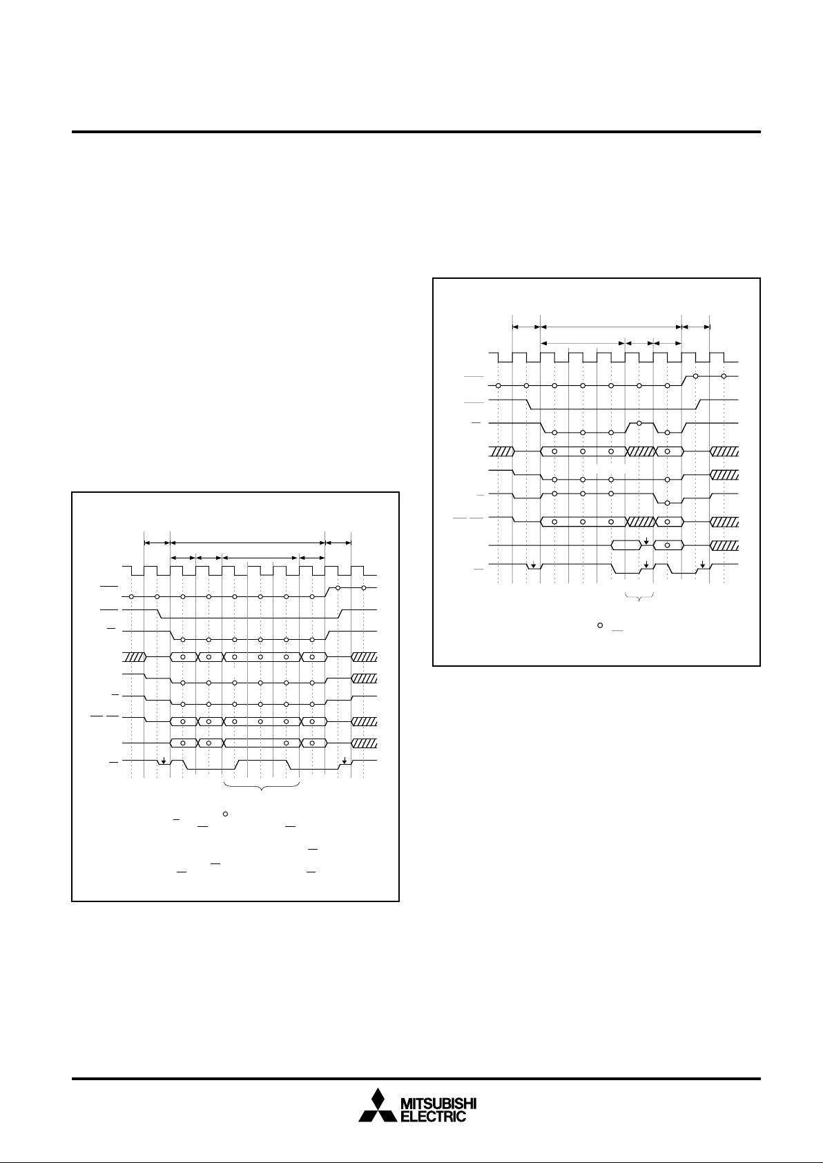
When the M32000D3FP is in the hold state and an "L" level is input
__
to CS, the M32000D3FP interprets it as a bus access request to the
internal DRAM. In this case, when the R/W signal is an "H" level, the
__
memory controller drives a read cycle to the internal DRAM. In the
read cycle, the 16-bit data for the address specified with A8 to A30,
is output from D0 to D15 regardless of the BCH and BCL settings.
Also the DC signal is output.
__
____ ___
The M32000D3FP reads 128 bits of data from the block on the 128bit boundary including the requested address into the 128-bit buffer
of the bus interface unit. 3 to 7 CLKIN clock periods are necessary
for the first bus access, however, when reading consecutive address
within the 128-bit boundary, the subsequent read bus cycles are completed in 1 CLKIN clock period because a read from the internal DRAM
does not take place. After DC outputs an "L" level (access complete),
__
return CS to the "H" level between the CLKIN falling edge corresponding to the last read cycle and the following CLKIN falling edge.
______
Return HREQ to the "H" level to return the M32000D3FP to the normal operation mode from the hold state either at the same time as or
__
after CS is returned to the "H" level.
__
MITSUBISHI MICROCOMPUTERS
M32000D3FP
SINGLE-CHIP 32-BIT CMOS MICROCOMPUTER
hold shift
CLKIN
HREQ
HACK
CS
A8 - A30
SID
R/W
BCH, BCL
D0 - D15
DC
Note: "Hi-z" means high impedance, and indicates sampling timing.
"Hi-z" "Hi-z"
"Hi-z" "Hi-z"
"Hi-z" "Hi-z"
"Hi-z" "Hi-z"
"Hi-z"
"Hi-z" "Hi-z"
The value of the R/W signal that controls the data direction of the bus interface
cannot be changed during CS="L". Hold this value while CS="L".
Also, where marked above with ✽, 3 to 7 CLKIN clock periods are necessary for
the first read operation (also when reading crosses an 128-bit boundary) when
reading from the internal DRAM. Hold the input value of the address or other control
signals during these wait cycle periods (DC = "H"). Consecutive read operations
within an 128-bit boundary are completed in 1 CLKIN clock period.
During these wait cycle period, CS cannot be returned to an "H" level (the access
cannot be aborted). CS can only be returned to an "H" level after DC is driven to "L".
hold
read read read read
("L" input)
("L" output)
✽
return
"Hi-z"
Fig. 23 Read bus cycle to internal DRAM
24
MITSUBISHI MICROCOMPUTERS
M32000D3FP
SINGLE-CHIP 32-BIT CMOS MICROCOMPUTER
When the M32000D3FP is in the hold state and an "L" level is input
__
to CS, the M32000D3FP interprets it as a bus access request to the
internal DRAM. In this case, when the R/W signal is at an "L" level,
the memory controller drives a write cycle to the internal DRAM. Byte
data control is specified by the BCH and BCL signals. Only data in
____ ___
the byte positions for which an "L" level is input to BCH or BCL are
written. When writing is complete, an "L" level DC signal is output.
__
____ ___
__
The M32000D3FP stores the requested data in the 128-bit data buffer
of the BIU, before writing to the internal DRAM. This reduces the
number of accesses to the internal DRAM when a request to writing
to consecutive addresses is made, and improves bus cycle throughput. Consecutive write cycles within an 128-bit boundary are completed in 1 CLKIN clock period. 3 to 7 CLKIN clock periods are necessary for a write access crossing an 128-bit boundary when writing
to the internal DRAM. After DC outputs an "L" level (access complete), return CS to the "H" level between the CLKIN falling edge
corresponding to the last write cycle and the following CLKIN falling
edge. Return HREQ to the "H" level to return the M32000D3FP to
the normal operation mode from the hold state either at the same
time as or after CS is returned to the "H" level.
CLKIN
A8 - A30
BCH, BCL
D0 - D15
Note: "Hi-z" means high impedance, and indicates sampling timing.
__
______
__
hold shift
HREQ
HACK
CS
"Hi-z" "Hi-z"
SID
R/W
"Hi-z" "Hi-z"
"Hi-z" "Hi-z"
"Hi-z" "Hi-z"
"Hi-z" "Hi-z"
DC
"Hi-z" "Hi-z"
The value of the R/W signal that controls the data direction of the bus interface
cannot be changed during CS="L". Hold this value while CS="L".
Also, where marked above with ✽, 3 to 7 CLKIN clock periods are necessary for writing
operation to internal DRAM crossing an 128-bit boundary. Hold the input value of the
address or other control signals during these wait cycle periods (DC = "H"). Consecutive
writing operations within an 128-bit boundary are completed in 1 CLKIN clock period.
During these wait cycle period, CS cannot be returned to "H" level (the access
cannot be aborted). CS can only be returned to a "H" level after DC is driven to "L".
__
hold return
write write write write
("L" output)
("L" output) ("L" output)
✽
When the external bus master makes an access, the value of the
__
R/W signal that controls the data direction of the bus interface cannot be changed during CS="L". Therefore, read cycles and write cycles
__
__
cannot be mixed while CS = "L". When starting a write cycle following after a read cycle and starting a read cycle following a write cycle,
__
keep the CS signal at an "H" level for at least 1 CLKIN.
hold shift
CLKIN
HREQ
HACK
CS
A8 - A30
SID
R/W
BCH, BCL
D0 - D15
DC
Note: "Hi-z" means high-impedance, and indicates sampling timing.
"Hi-z" "Hi-z"
"Hi-z" "Hi-z"
"Hi-z" "Hi-z"
"Hi-z"
"Hi-z" "Hi-z"
Also, where marked above with ✽, keep CS signal to "H" at least 1 CLKIN when
starting a write bus cycle after a read bus cycle or a read bus cycle after a write
bus cycle.
hold return
read CS = "H"
("L" input)
"Hi-z"
"Hi-z"
("L" output)
✽
write
"Hi-z""Hi-z"
"Hi-z"
("L" output)
Fig. 25 Read/write bus cycle
Fig. 24 Write bus cycle to internal DRAM
25

MITSUBISHI MICROCOMPUTERS
M32000D3FP
SINGLE-CHIP 32-BIT CMOS MICROCOMPUTER
Master/slave mode
The M32000D3FP has an M/S (master/slave) pin for multiprocessor
configuration use.
• master mode (M/S = "H")
This is normal operation mode. Set the M/S pin to an "H" level. It is
used when the M32000D3FP is used as the main CPU in a system.
• slave mode (M/S = "L")
This operation mode is for when the M32000D3FP is used as a
coprocessor. Set the M/S pin to an "L" level. When set to slave mode,
_
_
_
_
_
the M32000D3FP does not start operation even after a reset, until an
interrupt request or the SBI is input. Processing is carried out by
communicating with the master M32000D3FP, using the two programmable I/O ports and the external interrupt signal.
lock control register (MLCR) < address: H'FFFF FFF7>
D24 D25 D26 D27 D28 D29 D30 D31
LM
<at reset: H'00>
D bit name function R W
24 - 30 Not 0
assigned.
31 LM
(lock mode)
______
0: HREQ
exclusive
lock mode
___
✕
1: CS exclusive
lock mode
R = 0 ... "0" when reading R = ... read enabled
W = ... write enabled W = : write disabled
✕
• Coprocessor only configuration example
The slave M32000D3FP accesses only the internal DRAM and never
the external bus. M/S and HREQ are fixed at the "L" level. The slave
_ _____
M32000D3FP executes the instructions that the master M32000D3FP
downloads to the internal DRAM. The data transfer request (processing complete) from the slave M32000D3FP is notified to the master
M32000D3FP by inputting the interrupt request via the programmable
I/O port. The data transaction is carried out when the master
M32000D3FP accesses the internal DRAM in the slave M32000D3FP.
• Common bus coprocessor configuration example
In this configuration, the slave M32000D3FP can also access the
external bus. Communications between the master and slave CPUs
is carried out using the programmable I/O ports and the interrupt
request input.
<coprocessor only configuration>
no access to
external bus
M/SM/S HREQ
M32000D3FP
(master)
INT PP0
ROM
ASIC
INT
M32000D3FP
(slave)
<common bus coprocessor configuration>
Fig. 26 Lock control register
M/SM/S
HREQ
HACK
INT
ROM
M32000D3FP
(master)
ASIC
bus
arbiter
INT
M32000D3FP
(slave)
Fig. 27 Master/slave system configuration example
HREQ
HACK
PP0
26

MITSUBISHI MICROCOMPUTERS
M32000D3FP
SINGLE-CHIP 32-BIT CMOS MICROCOMPUTER
Power management function
The M32000D3FP has the following two low-power consumption
modes.
• standby mode
• CPU sleep mode
power management (MPMR) < address: H'FFFF FFFB>
D24 D25 D26 D27 D28 D29 D31
D bit name function R W
24 - 29 Not assigned. 0
30, 31 PM0, PM1
(low power
consumption
mode)
00: normal
operation
mode
01: (reserved)
10: CPU sleep
mode
11: standby mode
R = 0 ... "0" when reading R = ... read enabled
W = ... write enabled W = : write disabled
✕
D30
PM1
PM0
<at reset: H'00>
✕
In standby mode, all clock supply stops and only the contents of the
internal DRAM are retained. The power requirement is only that which
the internal DRAM needs for refreshing itself. When set to standby
mode, the M32000D3FP waits for the current bus operation to be
completed. It then purges the cache memory and switches the internal DRAM to self-refresh mode. After that, the PLL and all clock supplies stop and the STBY signal goes to an "L" level to indicate the
completion of the switch to standby mode. Input an "L" level to WKUP
___
or RST to return from standby mode to normal operation mode. The
contents of the internal DRAM are retained upon return using the
_____
WKUP signal.
_____
_____
In CPU sleep mode, clock supply to the M32R CPU stops. In this
mode, the internal DRAM, cache memory, memory controller and
external bus interface continue to operate and the internal DRAM
can be accessed from the external bus. Input an "L" level to INT, SBI
___
or RST to return to normal operation mode from CPU sleep mode.
___ ___
The contents of the cache memory, internal DRAM, general-purpose
registers and programmable I/O control register are retained upon
return using the INT or SBI signals.
___ ___
Fig. 28 Power management control register
set to standby mode
(H'03 is written to
MPMR register)
standby mode
operation mode
WKUP, RST
input
reset
normal
set to CPU sleep mode
(H'02 is written to
MPMR register)
INT, SBI, RST
input
CPU sleep
mode
Fig. 29 State transition for low power consumption mode
27
MITSUBISHI MICROCOMPUTERS
M32000D3FP
SINGLE-CHIP 32-BIT CMOS MICROCOMPUTER
Programmable I/O port
The M32000D3FP has two programmable I/O ports (PP0, PP1). Each
port can be set as input or output.
programmable I/O port direction control register 0 (PPCR0)
D24 D25 D26 D27 D28 D29 D30 D31
programmable I/O port direction control register 1 (PPCR1)
D24 D25 D26 D27 D28 D29 D30 D31
D bit name function R W
24 - 30 Not assigned. 0
31 PP0C, PP1C 0: input port
(port I/O direction) 1: output port
R = 0 ... "0" when reading R = ... read enabled
W = ... write enabled W = : write disabled
Fig. 30 Programmable I/O port direction control register
programmable I/O port data register 0 (PPDR0)
D24 D25 D26 D27 D28 D29 D30 D31
< address: H'FFFF FFE3>
PP0C
< address: H'FFFF FFE7>
PP1C
<at reset: H'00>
< address: H'FFFF FFEB>
PP0D
Reset
When an "L" level is input to RST, the M32000D3FP switches to the
reset state. The reset state is released when an "H" level is input to
____
RST, and the program is executed from the EIT vector entry of the
____
reset interrupt. All internal resources including the internal PLL (4x
clock generator) are initialized. In order to stabilize PLL oscillation,
the "L" input to RST should last a minimum of 2 ms after VCC stabi-
____
lizes to the specified voltage level.
Table 2 Internal state after reset
internal resources state
DRAM undefined
cache memory invalid
(purged all)
general purpose undefined
registers
(R0 - R15)
control registers PSW (CR0)
B'0000 0000 0000 0000 ??00 000? 0000 0000
(BSM, BIE, and BC are undefined)
CBR (CR1) H'0000 0000
SPI (CR2) undefined
SPU (CR3) undefined
BPC (CR6) undefined
PC
master mode:
execute from address H'7FFF FFF0
slave mode:
wait for interrupt input at address
H'7FFF FFF0
• execute from address H'0000 0010
by inputting SBI signal
• execute from address H'0000 0080
by inputting INT signal
___
___
ACC
(accumulator) undefined
I/O registers
PPCR0, PPCR1
PPDR0, PPDR1
MLCR
H'00 (input)
B'0000 000? (depends on input
pin state)
_____
H'00 (HREQ exclusive lock mode)
MPMR H'00 (normal operation)
MCCR H'01 (cache-off mode)
programmable I/O port data register 1 (PPDR1)
< address: H'FFFF FFEF>
D24 D25 D26 D27 D28 D29 D30 D31
PP1D
<at reset: B'0000 000?>
D bit name function R W
24 - 30 Not assigned. 0
31 PP0D, PP1D 0: data = "0"
(port data) 1: data = "1"
R = 0 ... "0" when reading R = ... read enabled
W = ... write enabled W = : write disabled
Fig. 31 Programmable I/O port data register
28

MITSUBISHI MICROCOMPUTERS
M32000D3FP
SINGLE-CHIP 32-BIT CMOS MICROCOMPUTER
Clock generating circuit
The M32000D3FP has a clock multiplier circuit and operates at four
times the input frequency. The internal operation frequency becomes
66.6 MHz when a 16.65 MHz clock is input to CLKIN. A capacitor (C)
should be connected to the PLLCAP pin, and the clock is input to the
CLKIN pin. The PLLVCC and PLLVSS pins should be connected to
the power source or the ground, respectively.
M32000D3FP
VCC
14 (PLLVCC)
PLL clock
generating
circuit
recommended values in circuit
C: 1000 pF
18 (CLKIN)
16 (PLLCAP)
15 (PLLVSS)
clock input
C
ADDRESSING MODE
M32R family supports the following addressing modes.
< register direct >
The general-purpose register or the control register to be processed
is specified.
< register indirect >
The contents of the register specify the address in memory to be
accessed. This mode can be used by all load/store instructions.
< register relative indirect >
(The contents of the register) + (16-bit immediate value which is signextended to 32 bits) specify the address in memory to be accessed.
< register indirect and register update >
• 4 is added to the register contents
(the contents of the register before update specify
the address in memory to be accessed [LD instruction]
• 4 is added to the register contents
(the contents of the register after update specify
the address in memory to be accessed) [ST instruction]
• 4 is subtracted from the register contents
(the contents of the register after update specify
the address in memory to be accessed) [ST instruction]
< immediate >
The 4-, 5-, 8-, 16- or 24-bit immediate value.
< PC relative >
(The contents of PC) + (8, 16, or 24-bit displacement which is signextended to 32 bits and 2 bits left-shifted) specify the address in
memory to be accessed.
Fig. 32 Oscillation circuit
29

MITSUBISHI MICROCOMPUTERS
M32000D3FP
SINGLE-CHIP 32-BIT CMOS MICROCOMPUTER
INSTRUCTION FORMAT
There are two major instruction formats: two 16-bit instructions packed
together within a word boundary, and a single 32-bit instruction.
< 16-bit instruction >
R
1
op1 R
1
op1 R
1
op1 cond c
< 32-bit instruction >
op1 R
1
op1 R
1
op1 R
1
op1 cond c
R
2
op2
c
R
2
op2 c
R
2
op2 c
Fig. 33 Instruction format
= R1 op R
R1 = R1 op c
Branch (Short Displacement)
c
2
R
1
= R2 op c
Compare and Branch
1
= R1 op c
R
Branch
INSTRUCTION SET
A total of 83 instructions are implemented.
<Load/store instructions>
The load/store instructions carry out data transfers between a register and a memory.
LD Load
LDB Load byte
LDUB Load unsigned byte
LDH Load halfword
LDUH Load unsigned halfword
LOCK Load locked
ST Store
STB Store byte
STH Store halfword
UNLOCK Store unlocked
<Transfer instructions>
The transfer instructions carry out data transfers between registers
or a register and an immediate value.
LD24 Load 24-bit immediate
LDI Load immediate
MV Move register
MVFC Move from control register
MVTC Move to control register
SETH Set high-order 16-bit
<Operation instructions>
Compare, arithmetic/logic operation, multiply and divide, and shift
are carried out between registers.
• compare instructions
CMP Compare
CMPI Compare immediate
CMPU Compare unsigned
CMPUI Compare unsigned immediate
• arithmetic operation instructions
ADD Add
ADD3 Add 3-operand
ADDI Add immediate
ADDV Add with overflow checking
ADDV3 Add 3-operand
ADDX Add with carry
NEG Negate
SUB Subtract
SUBV Subtract with overflow checking
SUBX Subtract with borrow
30

MITSUBISHI MICROCOMPUTERS
M32000D3FP
SINGLE-CHIP 32-BIT CMOS MICROCOMPUTER
• logic operation instructions
AND AND
AND3 AND 3-operand
NOT Logical NOT
OR OR
OR3 OR 3-operand
XOR Exclusive OR
XOR3 Exclusive OR 3-operand
• multiply/divide instructions
DIV Divide
DIVU Divide unsigned
MUL Multiply
REM Remainder
REMU Remainder unsigned
• shift instructions
SLL Shift left logical
SLL3 Shift left logical 3-operand
SLLI Shift left logical immediate
SRA Shift right arithmetic
SRA3 Shift right arithmetic 3-operand
SRAI Shift right arithmetic immediate
SRL Shift right logical
SRL3 Shift right logical 3-operand
SRLI Shift right logical immediate
<Branch instructions>
The branch instructions are used to change the program flow.
BC Branch on C-bit
BEQ Branch on equal
BEQZ Branch on equal zero
BGEZ Branch on greater than or equal zero
BGTZ Branch on greater than zero
BL Branch and link
BLEZ Branch on less than or equal zero
BLTZ Branch on less than zero
BNC Branch on not C-bit
BNE Branch on not equal
BNEZ Branch on not equal zero
BRA Branch
JL Jump and link
JMP Jump
NOP No operation
<EIT-related instructions>
The EIT-related instructions carry out the EIT events (Exception, Interrupt and Trap). Trap initiation and return from EIT are EIT-related
instructions.
TRAP Trap
RTE Return from EIT
<DSP function instructions>
The DSP function instructions carry out multiplication of 32 bits ✕ 16
bits and 16 bits ✕ 16 bits or multiply and add operation; there are
also instructions to round off data in the accumulator and carry out
transfer of data between the accumulator and a general-purpose register.
MACHI Multiply-accumulate high-order halfwords
MACLO Multiply-accumulate low-order halfwords
MACWHI Multiply-accumulate word and high-order halfword
MACWLO Multiply-accumulate word and low-order halfword
MULHI Multiply high-order halfwords
MULLO Multiply low-order halfwords
MULWHI Multiply word and high-order halfword
MULWLO Multiply word and low-order halfword
MVFACHI Move from accumulator high-order word
MVFACLO Move from accumulator low-order word
MVFACMI Move from accumulator middle-order word
MVTACHI Move to accumulator high-order word
MVTACLO Move to accumulator low-order word
RAC Round accumulator
RACH Round accumulator halfword
31

MITSUBISHI MICROCOMPUTERS
M32000D3FP
SINGLE-CHIP 32-BIT CMOS MICROCOMPUTER
ABSOLUTE MAXIMUM RATINGS
Symbol
VCC
VI
VO
PD
TOPR
TSTG
Power source voltage
Input voltage
Output voltage
Power consumption
Operating temperature
Storage temperature
Parameter
Conditions
TOPR = 25 °C
RECOMMENDED OPERATING CONDITIONS (VCC = 3.3 V ± 0.3 V, TOPR = 0 to 70 °C unless otherwise noted)
Symbol Parameter Unit
VCC
VIH
VIL
(see note)
IOH
IOL
(see note)
CL
Note: IOH and IOL represent the maximum values of DC current load. Intermittent current that is generated during output need not to be
considered as long as the output load capacity is within the specified range.
Power source voltage
“H” input voltage All inputs except following
“L” input voltage All inputs except following
“H” output current
“L” output current
output load capacity
____
RST pin
____
RST pin
Min.
3.0
2.0
0.8VCC
–0.3
–0.3
Min.
–0.5
–0.5
–0.5
0
–65
Ratings
Ratings
Typ.
Max.
4.6
4.6
4.6
1000
70
150
Max.
3.6
VCC+0.3
VCC+0.3
0.8
0.2VCC
2
2
50
Unit
V
V
V
mW
°C
°C
V
V
V
V
V
mA
mA
pF
32

MITSUBISHI MICROCOMPUTERS
M32000D3FP
SINGLE-CHIP 32-BIT CMOS MICROCOMPUTER
DC CHARACTERISTICS
ELECTRICAL CHARACTERISTICS
Symbol Parameter Unit
VOH
VOL
IOZ
IIH
IIL
ICC
C
“H” output voltage
“L” output voltage
Output current in off state
“H” input current
“L” input current
Power source current
Pin capacitance
(VCC = 3.3 V ± 0.3 V, TOPR = 0 to 70 °C unless otherwise noted)
Test conditions
IOH = –2 mA
IOL = 2 mA
VO = 0 to VCC
VIH = 0 to VCC +0.3 V
VIH = 0 to VCC +0.3 V
Average in normal operation
mode VCC = 3.3 V
Average in CPU sleep mode
VCC = 3.3 V
Average in standby mode
VCC = 3.3 V
All pins
Min.
2.4
–10.0
Ratings
Typ.
120
80
Max.
0.4
10.0
10.0
–10.0
200
150
1500
15
V
V
µA
µA
µA
mA
mA
µA
pF
33

AC CHARACTERISTICS
TIMING REQUIREMENTS
(1) Input transition time
Symbol Parameter
tr(INPUT)
tf(INPUT)
(2) Clock, reset and wakeup timing
Symbol Parameter
tc(CLKIN)
tw(CLKINH)
tw(CLKINL)
tr(CLKIN)
tf(CLKIN)
tw(RST)
tw(WKUP)
Input rise transition time
Input fall transition time
Clock input cycle time
External clock input “H” pulse width
External clock input “L” pulse width
External clock input rising time
External clock input falling time
Reset input “L” pulse width
Wakeup input “L” pulse width
(VCC = 3.3 ± 0.3 V, CL = 50 pF, TOPR = 0 to 70 °C unless otherwise noted)
Test conditions
CMOS input
____
RST pin
CMOS input
____
RST pin
Test conditions
MITSUBISHI MICROCOMPUTERS
M32000D3FP
SINGLE-CHIP 32-BIT CMOS MICROCOMPUTER
Min.
Min.
60
1/4CLKIN
1/4CLKIN
2
2
Limits
Max.
5
2
5
2
Limits
Max.
100
5
5
Unit
ns
ms
ns
ms
Unit
ns
ns
ns
ns
ns
ms
ms
Reference
number
1
2
Reference
number
5
6
7
8
9
10
11
(3) Read and write timing
Symbol Parameter
tsu(D-CLKIN)
th(CLKIN-D)
tsu(DCH-CLKIN)
th(CLKIN-DCH)
tsu(DCL-CLKIN)
th(CLKIN-DCL)
Data input set-up time before CLKIN
Data input hold time after CLKIN
__
DC input “H” set-up time before CLKIN
__
DC input “H” hold time after CLKIN
__
DC input “L” set-up time before CLKIN
__
DC input “L” hold time after CLKIN
Test conditions
Min.
5
2
10
2
10
2
Limits
Max.
Unit
ns
ns
ns
ns
ns
ns
Reference
number
30
31
36
37
38
39
34

MITSUBISHI MICROCOMPUTERS
M32000D3FP
SINGLE-CHIP 32-BIT CMOS MICROCOMPUTER
(4) Arbitration and external bus master read/write timing
Symbol
tsu(HREQ-CLKIN)
th(CLKIN-HREQ)
tsu(CS-CLKIN)
th(CLKIN-CS)
tsu(A-CLKIN)
th(CLKIN-A)
tsu(D-CLKINL)
th(CLKINL-D)
_____
HREQ input set-up time before CLKIN
_____
HREQ input hold time after CLKIN
__
CS input set-up time before CLKIN
__
CS input hold time after CLKIN
Address input set-up time before CLKIN
Address input hold time after CLKIN
Data input set-up time before CLKIN
Data input hold time after CLKIN
Parameter
Test conditions
(5) Interrupt control unit timing
Symbol Parameter
tw(INT)
tw(SBI)
___
INT input pulse width (see note)
___
SBI input pulse width (see note)
___ ___
Note: Both INT and SBI are level-sense inputs. Keep them at an "L" level until the interrupt is accepted.
Test conditions
Min.
5
2
10
2
5
3
5
3
Min.
tc(CLKIN)
tc(CLKIN)
Limits
Max.
Limits
Max.
Unit
ns
ns
ns
ns
ns
ns
ns
ns
Unit
ns
ns
Reference
number
40
41
48
49
50
51
52
53
Reference
number
63
64
(6) I/O port timing
Symbol Parameter
tw(PORTINL)
tw(PORTINH)
Port input “L” pulse width
Port input “H” pulse width
Test conditions
Min.
30
30
Limits
Max.
Unit
ns
ns
Reference
number
69
70
35
MITSUBISHI MICROCOMPUTERS
M32000D3FP
SINGLE-CHIP 32-BIT CMOS MICROCOMPUTER
SWITCHING CHARACTERISTICS (VCC = 3.3 ± 0.3 V, CL = 50 pF, TOPR = 0 to 70 °C unless otherwise noted)
(1) Output transition time
Symbol Parameter
tr(OUTPUT)
tf(OUTPUT)
Output rising transition time
Output falling transition time
(2) Read and write timing
Symbol
td(CLKIN-BSHX)
td(CLKIN-BSL)
td(CLKIN-BSLX)
td(CLKIN-BSH)
td(CLKIN-AV)
td(CLKIN-AX)
td(CLKIN-BCV)
td(CLKIN-BCX)
td(CLKIN-SIDV)
td(CLKIN-SIDX)
td(CLKIN-STV)
td(CLKIN-STX)
td(CLKIN-RWV)
td(CLKIN-RWX)
td(CLKIN-BURSTHX)
td(CLKIN-BURSTL)
td(CLKIN-BURSTLX)
td(CLKIN-BURSTH)
td(CLKIN-DZX)
td(CLKIN-DV)
td(CLKIN-DVX)
td(CLKIN-DXZ)
__
BS = “H” effective time after CLKIN
__
BS = “L” delay time after CLKIN
__
BS = “L” effective time after CLKIN
__
BS = “H” delay time after CLKIN
Address delay time after CLKIN
Address effective time after CLKIN
____ ___
BCH, BCL delay time after CLKIN
____ ___
BCH, BCL effective time after CLKIN
SID delay time after CLKIN
SID effective time after CLKIN
ST delay time after CLKIN
ST effective time after CLKIN
__
R/W delay time after CLKIN
__
R/W effective time after CLKIN
______
BURST = “H” effective time after CLKIN
______
BURST = “L” delay time after CLKIN
______
BURST = “L” effective time after CLKIN
______
BURST = “H” delay time after CLKIN
Data output enable time after CLKIN
Data output delay time after CLKIN
Data output effective time after CLKIN
Data output disable time after CLKIN
Parameter
Test conditions
Test
conditions
Min.
Min.
0
tc(CLKIN)/4
0
0
0
0
0
0
0
0
0
Limits
Typ.
Max.
8
8
Limits
Max.
12
tc(CLKIN)/4+8
16
16
16
16
16
12
12
18
16
Unit
ns
ns
Unit
ns
ns
ns
ns
ns
ns
ns
ns
ns
ns
ns
ns
ns
ns
ns
ns
ns
ns
ns
ns
ns
ns
Reference
number
3
4
Reference
number
12
13
14
15
16
17
18
19
20
21
22
23
24
25
26
27
28
29
32
33
34
35
36

(3) Arbitration and external bus master read/write timing
Symbol Test conditions
td(CLKIN-HACKHX)
td(CLKIN-HACKL)
td(CLKIN-HACKLX)
td(CLKIN-HACKH)
td(CLKIN-AZ)
td(CLKIN-AZX)
td(CLKIN-DZX)
td(CLKIN-DV)
td(CLKIN-DXZ)
td(CLKIN-DVX)
td(CS-DCZX)
td(CLKIN-DCHX)
td(CLKIN-DCL)
td(CLKIN-DCXZ)
td(CLKIN-DCLX)
_____
HACK = “H” effective time after CLKIN
_____
HACK = “L” delay time after CLKIN
_____
HACK = “L” effective time after CLKIN
_____
HACK = “H” delay time after CLKIN
Address output disable time after CLKIN
Address output enable time after CLKIN
Data output enable time after CLKIN
Data output delay time after CLKIN
Data output disable time after CLKIN
Data output effective time after CLKIN
__ __
DC output enable time after CS
__
DC = “H” effective time after CLKIN
__
DC = “L” delay time after CLKIN
__
DC output disable time after CLKIN
__
DC = “L” effective time after CLKIN
Parameter
MITSUBISHI MICROCOMPUTERS
M32000D3FP
SINGLE-CHIP 32-BIT CMOS MICROCOMPUTER
Min.
0
0
0
0
0
0
0
0
Limits
Max.
12
12
16
18
16
16
16
Unit
ns
ns
ns
ns
ns
ns
ns
ns
ns
ns
ns
ns
ns
ns
ns
Reference
number
42
43
44
45
46
47
54
55
56
57
58
59
60
61
62
(4) Standby timing
Symbol Test conditions
td(CLKIN-STBYHX)
td(CLKIN-STBYL)
td(CLKIN-STBYLX)
td(CLKIN-STBYH)
Note: The STBY signal is synchronized with the internal clock, therefore its timing changes at 0, 90, 180 and 270 (n=0, 1, 2, 3) degree phase
_____
_____
STBY = “H” effective time after CLKIN
_____
STBY = “L” delay time after CLKIN (see note)
_____
STBY = “L” effective time after CLKIN
_____
STBY = “H” delay time after CLKIN (see note)
Parameter
Min.
Limits
Max.
0
tc(CLKIN)n/4+15
0
tc(CLKIN)n/4+15
of CLKIN.
Unit
ns
ns
ns
ns
Reference
number
65
66
67
68
(5) I/O port timing
Symbol Parameter
tw(PORTOUTL)
tw(PORTOUTH)
Port output “L” pulse width (see note)
Port output “H” pulse width (see note)
Test conditions
Min.
12
12
Limits
Max.
Note: The minimum pulse width value is that where the output is changed within 1 clock of the internal clock. Software processing time to write
to the port data register is not included.
Unit
ns
ns
Reference
number
71
72
37

MITSUBISHI MICROCOMPUTERS
M32000D3FP
SINGLE-CHIP 32-BIT CMOS MICROCOMPUTER
0.5V
CC
measured pin
CL = 50 pF
CMOS output CMOS output
Fig. 34 Output switching characteristic measurement circuit
CMOS input
schmitt trigger input
"H" input level
"L" input level
"H" input level
"L" input level
0.9VCC
0.1VCC
VCC
0.0 V
measured pin
1.0 kΩ
CL = 50 pF
during floating delay time measurement)
(
timing reference point
(when not specified)
0.8VCC
0.2VCC
0.9VCC
0.1VCC
CLKIN input
"H" input level
"L" input level
Fig. 35 Input waveform and timing reference point during characteristic measurement
VCC
0.0 V
timing reference point
CMOS output (when not specified)
"H" → "Z"
CMOS output
(during floating delay time measurement)
"L" → "Z"
Fig. 36 Output timing measurement point during characteristic measurement
0.9VCC
0.1VCC
0.8VCC
0.2VCC
"Z" → "H"
0.6VCC
0.4VCC
"Z" → "L"
38

MITSUBISHI MICROCOMPUTERS
M32000D3FP
SINGLE-CHIP 32-BIT CMOS MICROCOMPUTER
CMOS input
(except for schmitt trigger input and CLKIN input)
schmitt trigger input
(RST)
Fig. 37 Input transition time
Fig. 38 Output transition time
output pin
1
1
3 4
t
r(OUTPUT)
t
r(INPUT)
t
r(INPUT)
t
f(OUTPUT)
2
2
0.8VCC
0.2VCC
t
f(INPUT)
t
f(INPUT)
0.8VCC
0.2VCC
0.9VCC
0.1VCC
CLKIN
RST
WKUP
Fig. 39 Clock reset and wakeup timing
(input)
(input)
(input)
5
t
c(CLKIN)
6
t
w(CLKINH)tw(CLKINL)
0.5VCC
*1 The WKUP and RST signals can be input asynchronously.
When returning from standby mode, the same timing applies.
7
10
11
8 9
t
w(RST)
t
w(WKUP)
t
r(CLKIN)
*1
*1
t
f(CLKIN)
0.8VCC
0.2VCC
39

MITSUBISHI MICROCOMPUTERS
M32000D3FP
SINGLE-CHIP 32-BIT CMOS MICROCOMPUTER
CLKIN
BS
A8 to A30
BCH, BCL
SID, ST
R/W
(input)
12
t
d(CLKIN-BSHX)
13
t
d(CLKIN-BSL)
(output)
(output)
(output)
(output)
(output)
0.5 VCC
16
18
20
22
24
0.5 VCC
t
d(CLKIN-AV)
t
d(CLKIN-BCV)
t
d(CLKIN-SIDV)
t
d(CLKIN-STV)
t
d(CLKIN-RWV)
14
t
d(CLKIN-BSLX)
15
t
d(CLKIN-BSH)
17
t
d(CLKIN-AX)
19
t
d(CLKIN-BCX)
*2
*2
21
t
d(CLKIN-SIDX)
23
t
d(CLKIN-STX)
25
t
d(CLKIN-RWX)
26
t
d(CLKIN-BURSTHX)
27
t
d(CLKIN-BURSTL)
BURST
D0 to D15
D0 to D15
DC
(output)
30
t
su(D-CLKIN)
31
(input)
32
t
d(CLKIN-DZX)
33
t
d(CLKIN-DV)
(output)
36
t
su(DCH-CLKIN)
37
*1
t
h(CLKIN-DCH)
*1
38
t
su(DCL-CLKIN)
39
(input)
*1 The set up/hold of DC = "H" may vary depending on the wait cycle insertion or when an idle cycle occurs.
*2 All switching characteristics and timing requirements based on the falling edge of CLKIN are calculated according to
the internal CLKIN (duty ratio is 50%) . When designing external peripheral circuits, the correction for the duty cycle of
the actual CLKIN is necessary.
[example]
BS signal transition ("L" –> "H") when inputting 16.65 MHz clock whose duty ratio is 45 - 55% (± 5%) to CLKIN:
• minimum value of td(CLKIN-BSLX) = (value in table) – (correction value) = 15 – (60 x 5/100) = 12 [ns]
• maximum value of td(CLKIN-BSH) = (value in table) + (correction value) = (60/4 + 8) + (60 x 5/100) = 26 [ns]
*2
*2
t
h(CLKIN-D)
34
t
d(CLKIN-DVX)
35
t
d(CLKIN-DXZ)
t
h(CLKIN-DCL)
28
t
d(CLKIN-BURSTLX)
29
t
d(CLKIN-BURSTH)
*2
*2
Fig. 40 Read/write timing
40

0.5VCC 0.5VCC
MITSUBISHI MICROCOMPUTERS
M32000D3FP
SINGLE-CHIP 32-BIT CMOS MICROCOMPUTER
CLKIN
HREQ
HACK
(input)
(input)
(output)
40
t
su(HREQ-CLKIN)
42
t
d(CLKIN-HACKHX)
43
t
d(CLKIN-HACKL)
*1 *1
41
t
h(CLKIN-HREQ)
*2
*2
46
t
d(CLKIN-AZ)
44
t
d(CLKIN-HACKLX)
t
d(CLKIN-HACKH)
45
t
d(CLKIN-AZX)
47
*2
*2
A8 to A30, SID, ST,
BS, BCH, BCL,
R/W, BURST
(output)
*1 The HREQ signal can be input asynchronously.
*2 All switching characteristics and timing requirements based on the falling edge of CLKIN are calculated according to
the internal CLKIN (duty ratio is 50%) . When designing external peripheral circuits, the correction for the duty cycle of
the actual CLKIN is necessary.
[example]
HACK signal transition ("H" –> "L") when inputting 16.65 MHz clock whose duty ratio is 45 - 55% (± 5%) to CLKIN:
• minimum value of td(CLKIN-HACKHX) = (value in table) – (correction value) = 0 – (60 x 5/100) = –3 [ns]
• maximum value of td(CLKIN-HACKL) = (value in table) + (correction value) = 12 + (60 x 5/100) = 15 [ns]
Fig. 41 Bus arbitration timing
41

CLKIN
(input)
HREQ
(input)
HACK
(output)
0.5 VCC
40
t
su(HREQ-CLKIN)
MITSUBISHI MICROCOMPUTERS
M32000D3FP
SINGLE-CHIP 32-BIT CMOS MICROCOMPUTER
*1
49
t
h(CLKIN-CS)
*1
*1
*1
48 49
42
48
t
su(CS-CLKIN)
t
d(CLKIN-HACKHX)
43
t
d(CLKIN-HACKL)
*1
41
44
t
d(CLKIN-HACKLX)
45
t
d(CLKIN-HACKH)
48 49
t
h(CLKIN-HREQ)
*1
*1
*1
CS
(input)
R/W
(input)
A8 to A30
BCH, BCL
(input)
D0 to D15
(input)
D0 to D15
(output)
DC
(output)
58
t
d(CS-DCZX)
50
t
su(A-CLKIN)
54
t
d(CLKIN-DZX)
55
t
d(CLKIN-DV)
59
t
d(CLKIN-DCHX)
60
t
d(CLKIN-DCL)
*1 *1
51
t
h(CLKIN-A)
50 51 50 51
52 53
t
su(D-CLKINL)
*1
*1
56
t
d(CLKIN-DXZ)
57
t
d(CLKIN-DVX)
*1
*1
61
t
d(CLKIN-DCXZ)
62
t
d(CLKIN-DCLX)
*1
51
50
*1 *1
t
h(CLKINL-D)
*1
*1
58
*1
*1
59
60
61
62
*1 All switching characteristics and timing requirements based on the falling edge of CLKIN are calculated according to
the internal CLKIN (duty ratio is 50%) . When designing external peripheral circuits, the correction for the duty cycle of
the actual CLKIN is necessary.
[example]
CS signal transition ("L" –> "H") when inputting 16.65 MHz clock whose duty ratio is 45 - 55% (± 5%) to CLKIN:
• minimum value of tsu(CS-CLKIN) = (value in table) + (correction value) = 10 + (60 x 5/100) = 13 [ns]
• minimum value of th(CLKIN-CS) = (value in table) + (correction value) = 2 + (60 x 5/100) = 5 [ns]
Fig. 42 External bus master read/write timing
42

MITSUBISHI MICROCOMPUTERS
M32000D3FP
SINGLE-CHIP 32-BIT CMOS MICROCOMPUTER
INT
SBI
Fig. 43 Interrupt input timing
CLKIN
internal clock
(66.6 MHz)
t
w(INT)
t
w(SBI)
*1
*1
63
(input)
64
(input)
*1 The INT and SBI signals can be input asynchronously.
When returning from CPU sleep mode, the same timing applies.
This timing value is "a value necessary for sampling the input to pins", however, not "a value
that guarantees the interrupt acceptance".
The interrupt request is a level-sensed input , and should be kept "L" until it is accepted.
(input)
Fig. 44 Standby timing
STBY
[for input]
PX
[for output]
PX
67
t
65
t
d(CLKIN-STBYHX)
66
t
d(CLKIN-STBYL)
(output)
*1 The STBY signal is synchronized with the internal clock therefore, its timing changes at 0, 90, 180 and 270
degree phase of CLKIN.
*2 The STBY goes to an "L" level when switched to the standby mode.
*3 When returning from standby mode, the STBY signal goes to an "H" level 1 CLKIN after
sampling that WKUP has returned from "L" to "H", or 3 CLKINs after sampling that RST = "L".
69 70
t
w(PORTINL)
71 72
t
w(PORTOUTL)
*1 *2
t
w(PORTINH)
t
w(PORTOUTH)
d(CLKIN-STBYLX)
68
t
d(CLKIN-STBYH)
*1 *3
Fig. 45 I/O port timing
43

MITSUBISHI MICROCOMPUTERS
M32000D3FP
SINGLE-CHIP 32-BIT CMOS MICROCOMPUTER
Keep safety first in your circuit designs!
• Mitsubishi Electric Corporation puts the maximum effort into making semiconductor products better and more reliable, but there is always the possibility that trouble may occur with them. Trouble with
semiconductors may lead to personal injury, fire or property damage. Remember to give due consideration to safety when making your circuit designs, with appropriate measures such as (i) placement of
substitutive, auxiliary circuits, (ii) use of non-flammable material or (iii) prevention against any malfunction or mishap.
Notes regarding these materials
• These materials are intended as a reference to assist our customers in the selection of the Mitsubishi semiconductor product best suited to the customer’s application; they do not convey any license under any
intellectual property rights, or any other rights, belonging to Mitsubishi Electric Corporation or a third party.
• Mitsubishi Electric Corporation assumes no responsibility for any damage, or infringement of any third-party’s rights, originating in the use of any product data, diagrams, charts or circuit application examples
contained in these materials.
• All information contained in these materials, including product data, diagrams and charts, represent information on products at the time of publication of these materials, and are subject to change by Mitsubishi
Electric Corporation without notice due to product improvements or other reasons. It is therefore recommended that customers contact Mitsubishi Electric Corporation or an authorized Mitsubishi Semiconductor
product distributor for the latest product information before purchasing a product listed herein.
• Mitsubishi Electric Corporation semiconductors are not designed or manufactured for use in a device or system that is used under circumstances in which human life is potentially at stake. Please contact
Mitsubishi Electric Corporation or an authorized Mitsubishi Semiconductor product distributor when considering the use of a product contained herein for any specific purposes, such as apparatus or systems for
transportation, vehicular, medical, aerospace, nuclear, or undersea repeater use.
• The prior written approval of Mitsubishi Electric Corporation is necessary to reprint or reproduce in whole or in part these materials.
• If these products or technologies are subject to the Japanese export control restrictions, they must be exported under a license from the Japanese government and cannot be imported into a country other than the
approved destination.
Any diversion or reexport contrary to the export control laws and regulations of Japan and/or the country of destination is prohibited.
• Please contact Mitsubishi Electric Corporation or an authorized Mitsubishi Semiconductor product distributor for further details on these materials or the products contained therein.
© 1998 MITSUBISHI ELECTRIC CORP.
Revised edition, effective May. 1998.
Specifications subject to change without notice.

REVISION DESCRIPTION LIST M32000D3FP DATA SHEET
Rev. Rev.
Revision Description
No. date
1.0 First Edition 970507
2.0__• DC signal explanation revised (page 19). 970901
• Figures 17 to 25 revised (page 21 to page 25).
• 2 to 7 CLKIN clock periods are ~ → 3 to 7 CLKIN clock periods are ~ (left column in page 24)
• 2 to 7 CLKIN clock periods are ~ → 3 to 7 CLKIN clock periods are ~ (left column in page 25)
• DC CHARACTERISTICS, AC CHARACTERISTICS, and SWITCHING CHARACTERISTICS
revised (page 33 to 37).
• Figures 40 to 43 revised (page 40 to 43).
2.1__• "After DC outputs an ~ CLKIN falling edge." revised (line 14, page 24). 980501
• Notes in Figure 23 revised (page 24).
__
• "After DC outputs an ~ CLKIN falling edge." revised (line 15, page 25).
• Notes in Figure 24 revised (page 25).
• Table 2 revised (page 28).
• (3) Arbitration and external bus master read/write timing
Symbol Parameter
~~ ~
td(CS-DCZX) DC output enable time after CS corrected (page 37).
__ __
•" 58 td(CS-DCZX) *1 " in Fig. 42 corrected (page 42).
• Notes in Figure 44 revised (page 43).
(1/1)
 Loading...