


MITSUBISHI MICROCOMPUTERS
M306V2ME-XXXFP
SINGLE-CHIP 16-BIT CMOS MICROCOMPUTER with CLOSED CAPTION DECODER
1. DESCRIPTION
The M306V2ME-XXXFP and M306V2EEFP are single-chip microcomputers using the high-performance
silicon gate CMOS process using a M16C/60 Series CPU core and are packaged in a 100-pin plastic
molded QFP. These single-chip microcomputers operate using sophisticated instructions featuring a high
level of instruction efficiency. With 1M bytes of address space, they are capable of executing instructions at
high speed. They also feature a built-in OSD display function and data slicer, making them ideal for controlling TV with a closed caption decoder.
The features of the M306V2EEFP are similar to those of the M306V2ME-XXXFP except that this chip has
a built-in PROM which can be written electrically.
1.1 Features
• Memory size ........................................<ROM>192K bytes
<RAM> 5K bytes
<OSD ROM> 61K bytes
<OSD RAM> 2.2K bytes
• Shortest instruction execution time......100 ns (f(XIN)=10 MHz)
• Power sourse voltage ..........................4.5 V to 5.5V
• Power consumption .............................250 mW
• Interrupts..............................................21 internal and 3 external interrupt sources, 4 software
interrupt sources; 7 levels
• Multifunction 16-bit timer......................2 output timers + 3 input timers + 3 timers
• Serial I/O..............................................3 units
UART/clock synchronous: 2
Multi-master I2C-BUS interface 0 (2 systems): 1
Multi-master I2C-BUS interface 1 (1 system): 1
• DMAC ..................................................2 channels (trigger: 23 sources)
• A-D converter.......................................8 bits ✕ 6 channels
• D-A converter.......................................8 bits ✕ 2 channels
• Data slicer............................................1 circuit
• HSYNC counter .....................................1 circuit (2 systems)
• OSD function .......................................1 circuit
• Watchdog timer....................................1 circuit
• Programmable I/O ...............................78 lines
• Memory expansion ..............................Available
• Chip select output ................................4 lines
• Clock generating circuit .......................3 built-in clock generation circuits
and ON-SCREEN DISPLAY CONTROLLER
M306V2EEFP
1.2 Applications
TV with a closed caption decoder
Rev. 1.0
1

MITSUBISHI MICROCOMPUTERS
M306V2ME-XXXFP
M306V2EEFP
SINGLE-CHIP 16-BIT CMOS MICROCOMPUTER with CLOSED CAPTION DECODER
and ON-SCREEN DISPLAY CONTROLLER
------Table of Contents------
1. DESCRIPTION ..............................................1
1.1 Features...................................................1
1.2 Applications .............................................1
1.3 Pin Configuration ..................................... 3
1.4 Block Diagram .........................................4
1.5 Performance Outline................................5
2. OPERATION OF FUNCTIONAL BLOCKS .... 9
2.1 Memory....................................................9
2.2 Central Processing Unit (CPU) .............. 15
2.3 Reset .....................................................18
2.4 Processor Mode..................................... 23
2.5 Clock Generating Circuit........................36
2.6 Protection............................................... 46
2.7 Interrupts................................................ 47
2.8 Watchdog Timer ....................................67
2.9 DMAC .................................................... 69
2.10 Timer.................................................... 79
2.11 Serial I/O..............................................99
2.12 A-D Converter....................................149
2.13 D-A Converter....................................164
2.14 Data Slicer ......................................... 166
2.15 HSYNC Counter ..................................176
2.16 OSD Function .................................... 177
2.16.1 Triple Layer OSD ........................183
2.16.2 Display Position .......................... 185
2.16.3 Dot Size ...................................... 189
2.16.4 Clock for OSD.............................190
2.16.5 Field Determination Display........191
2.16.6 Memory for OSD.........................193
2.16.7 Character Color ..........................206
2.16.8 Character Background Color ...... 206
2.16.9 OUT1, OUT2 Signals..................211
2.16.10 Attribute ....................................212
2.16.11
2.16.12 Particular OSD Mode Block ...... 218
2.16.13 Multiline Display........................220
2.16.14 SPRITE OSD Function ............. 221
2.16.15 Window Function ...................... 224
2.16.16 Blank Function .......................... 225
2.16.17 Raster Coloring Function ..........228
Automatic Solid Space Function.....
217
2.16.18 Scan Mode................................230
2.16.19 R, G, B Signal Output Control... 230
2.16.20 OSD Reserved Register ........... 231
2.17 Programmable I/O Ports .................... 232
3. USAGE PRECAUTION..............................245
3.1 Timer A (timer mode)...........................245
3.2 Timer A (event counter mode) ............. 245
3.3 Timer A (one-shot timer mode)............245
3.4 Timer A
3.5 Timer B
3.6 Timer B (pulse period/pulse width
measurement mode) ...........................246
3.7 A-D Converter......................................246
3.8 Stop Mode and Wait Mode .................. 246
3.9 Interrupts..............................................247
3.10 Built-in PROM version .......................248
4. ITEM TO BE SUBMITTED WHEN ORDERING
MASKED ROM VERSION ......................... 249
5. ELECTRICAL CHARACTERISTICS..........250
5.1 Absolute Maximum Ratings ................. 250
5.2 Recommended Operating Conditions..251
5.3 Electrical Characteristics .....................252
5.4 A-D Conversion Characteristics........... 253
5.5 D-A Conversion Characteristics........... 253
5.6 Analog R, G, B Output Characteristics 253
5.7 Timing Requirements...........................254
5.8 Switching Characteristics.....................255
5.9 Measurement Circuit............................259
5.10 Timing Diagram .................................260
6. MASK ROM CONFIRMATION FORM ....... 265
7. MARK SPECIFICATION FORM ................269
8.ONE TIME PROM VERSION
M306V2EEFP MARKING...........................270
9. PACKAGE OUTLINE ................................. 271
(pulse width modulation mode)....
(timer mode, event counter mode) .....
245
246
Rev. 1.0
2
SINGLE-CHIP 16-BIT CMOS MICROCOMPUTER with CLOSED CAPTION DECODER
C
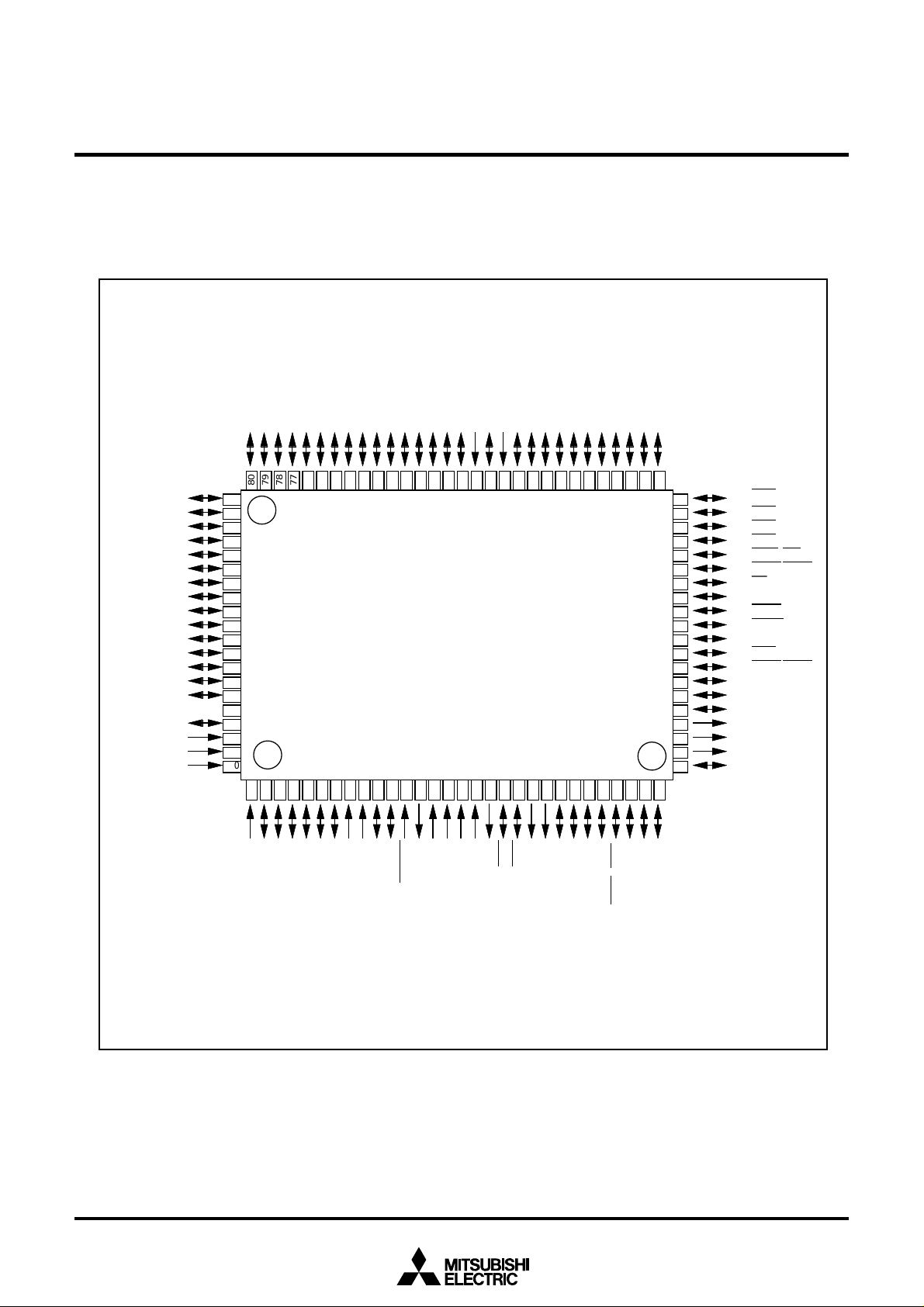
1.3 Pin Configuration
Figure 1.3.1 shows the pin configuration (top view).
PIN CONFIGURATION (top view)
)
)
0
1
)
D
D
/
/
/
0
1
2
D
D
0
1
2
3
8
9
1
D
D
D
/
/
/
0
1
2
1
1
1
P
P
P
8
0
9
8
7
07/ D
1
1
1
1
1
1
1
1
V S E T
7
06/ D
6
05/ D
5
04/ D
4
03/ D
3
02/ D
2
01/ D
1
00/ D
0
07/ A N
5
06/ A N
4
05/ A N
3
04/ A N
2
03/ A N
1
02/ A N
0
01/ V
S Y N
. C
. 3
00/ H
S Y N C
B 3
V c
c 3
V
I N
1P
2P
3P
4P
5P
6P
7P
8P
9P
0P
1P
9 2P
9 3P
9 4P
9 5P
9 6N
7P
8T
9 9A
0
0C
1
2
37
4
1
1
1
1
D
D
D
D
/
/
/
/
3
4
5
6
1
1
1
1
P
P
P
P
7
6
5
4
7
7
7
47
5
6
7
D
5
(
(
(
1
0
1
2
D
A
A
A
/
/
/
/
7
0
1
2
1
2
2
2
P
P
P
P
-
/
/
/
3
2
1
0
7
7
7
7
M 3 0 6 V 2 M E - X X X F P
M 3 0 6 V 2 E E F P
0
1
8
9
1
1
MITSUBISHI MICROCOMPUTERS
M306V2ME-XXXFP
M306V2EEFP
and ON-SCREEN DISPLAY CONTROLLER
)1
)
)1
)1
2
D
/
3
D
(
3
A
/
3
2
P
/
/
9
6
2
)1
3
4
5
6
D
D
/
/
4
5
D
D
(
(
4
5
A
A
/
/
4
5
2
2
P
P
/
/
8
7
6
6
3
4
1
)1
D
D
7
/
/
6
7
D
D
D
(
(
(
6
7
8
A
A
A
/
/
/
6
7
0
c
s1
2
2
3
V
c
P
P
/
6
5
6
6
5
6
V
s
P
/ - /
4
3
2
6
6
6
7
8
9
1
2
3
4
5
1
0
9
1
1
1
1
A
A
A
A
A
/
/
/
/
/
1
3
4
5
2
3
3
3
3
3
P
P
P
P
P
1
0
9
8
6
0
2
7
6
5
5
5
1
2
3
4
2
2
2
2
7
6
8
1
1
A
A
/
/
6
7
3
3
P
P
6
5
5
5
5
6
2
2
9
1
1
1
1
A
A
A
A
/
/
/
/
1
0
2
3
4
4
4
4
P
P
P
P
4
3
2
1
5
5
5
5
5 0
4 9
4 8
4 7
4 6
4 5
4 4
4 3
4 2
4 1
4 0
3 9
3 8
3 7
3 6
5
3 4
3
2
3 1
7
8
9
0
2
2
2
3
P 44/ C S 08
P 45/ C S 18
P 46/ C S 28
P 47/ C S 38
P 50/ W R L / W R8
P 51/ W R H / B H E8
P 52/ R D8
P 53/ B C L K8
P 54/ H L D A8
P 55/ H O L D9
P 56/ A L E9
P 57/ R D Y / C L K
P 60/ C T S0/ R T S
P 61/ C L K
0
P 62/ R x D
0
P 63/ TXD
0
B9
G9
R
P 67/ S D A 21
O U T
0
D
H
V
L
O L
N
N
N
3
3
F
I
I
I
2
1
H
/
1
A
/D
4
9
P
S D A
S C L
0
/
/
/
/
2
1
0
0
A
/D
3
9
P
Y T
9
9
9
P
P
P
T B
T B
T B
Figure 1.3.1 Pin configuration (top view)
Rev. 1.0
1
s
N
E
C
X
/
B
7
C
8
P
N V s
I
O U
S
C
N
T
I
S
C
X
O
V
C
X
/
R
U
6
8
P
E S E
V
X
S C
T
T
0
1
2
T
T
/
/
3
2
O
O
8
8
P
P
S C
U T
I N
I N
T
1
1
2
O
3
/
7
O
O
7
/
P
U T
6
7
P
H C
H C
T A
U
2
2
2
T
0
/
5
7
P
T A
U
2
K
S
D
D
O
2
/
4
7
P
C T
R T
X
X
T
R
,
2
S
/
/
/
/
2
0
1
3
7
7
7
7
P
P
P
P
S D A 1 /
S C L 1 /
S C L 2 / C L
Package: 100P6S-A
3
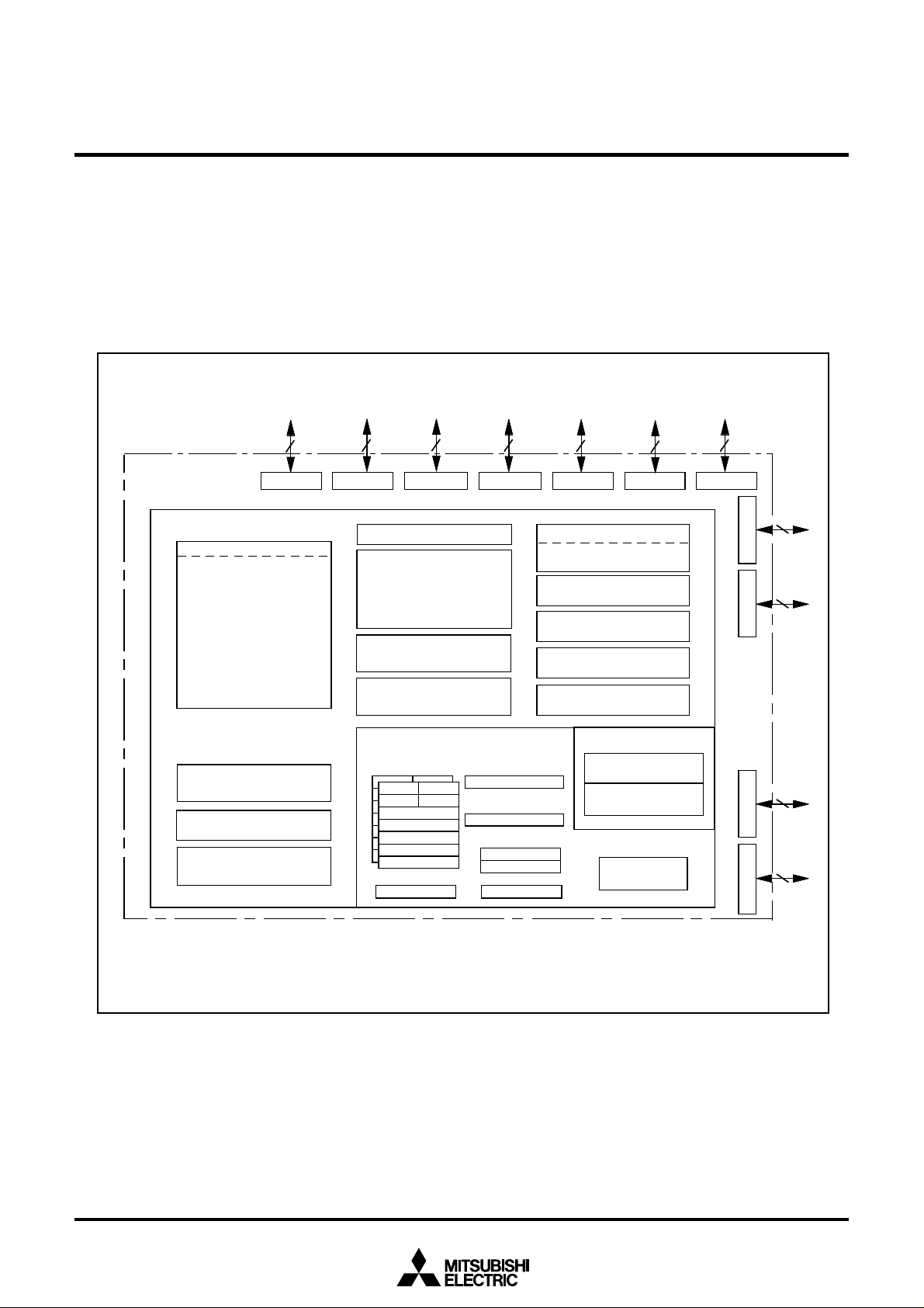
1.4 Block Diagram
0
Figure 1.4.1 is a block diagram.
MITSUBISHI MICROCOMPUTERS
M306V2ME-XXXFP
M306V2EEFP
SINGLE-CHIP 16-BIT CMOS MICROCOMPUTER with CLOSED CAPTION DECODER
and ON-SCREEN DISPLAY CONTROLLER
5
I / O p o r t s
I n t e r n a l p e r i p h e r a l f u n c t i o n s
T i m e r T A 0 ( 1 6 b i t s )
T i m e r T A 1 ( 1 6 b i t s )
T i m e r T A 2 ( 1 6 b i t s )
T i m e r T A 3 ( 1 6 b i t s )
T i m e r T A 4 ( 1 6 b i t s )
T i m e r T B 0 ( 1 6 b i t s )
T i m e r T B 1 ( 1 6 b i t s )
T i m e r T B 2 ( 1 6 b i t s )
W a t c h d o g t i m e r
( 2 c h a n n e l s )
D - A c o n v e r t e r
( 8 b i t s X 2 c h a n n e l s )
P o r t P 08P o r t P 18P o r t P 28P o r t P 38P o r t P 48P o r t P 58P o r t P 6
T i m e r
( 1 5 b i t s )
D M A C
A - D c o n v e r t e r
O S D
D a t a s l i c e r
H
S Y N C
c o u n t e r
M 1 6 C / 6 0 s e r i e s 1 6 - b i t C P U c o r e
R e g i s t e r s
R 0 LR 0 H
R 0 LR 0 H
R 1 HR 1 L
R 1 HR 1 L
R 2
R 2
R 3
R 3
A
A 0
A 1
A 1
F B
F B
S B F L G
P r o g r a m c o u n t e r
V e c t o r t a b l e
S t a c k p o i n t e r
S y s t e m c l o c k g e n e r a t o r
I N
– X
X
U A R T / c l o c k s y n c h r o n o u s S I / O
U A R T / c l o c k s y n c h r o n o u s S I / O
M u l t i - m a s t e r I2C - b u s
i n t e r f a c e 0
M u l t i - m a s t e r I2C - b u s
i n t e r f a c e 1
P C
I N T B
I S P
U S P
O U T
M e m o r y
R O M
1 9 2 K
R A M
5 K
M u l t i p l i e r
o r t P
P
7
o r t P
P
8 4
8
o r t P
P
9
5 8
o r t P 1
P
0
Figure 1.4.1 Block diagram
Rev. 1.0
4
MITSUBISHI MICROCOMPUTERS
M306V2ME-XXXFP
SINGLE-CHIP 16-BIT CMOS MICROCOMPUTER with CLOSED CAPTION DECODER
and ON-SCREEN DISPLAY CONTROLLER
1.5 Performance Outline
Table 1.5.1 is a performance outline.
Table 1.5.1 Performance outline
Item Performance
Number of basic instructions 91 instructions
Shortest instruction execution time 100 ns(f(XIN)=10 MHz)
Memory ROM 192K bytes
size RAM 5K bytes
OSD ROM 61K bytes
OSD RAM 2.2K bytes
I/O port P0 to P10 8 bits ✕ 8, 5 bits ✕ 2, 4 bits ✕ 1
Multifunction TA0, TA1, TA2, TA3, TA4 16 bits ✕ 5
timer TB0, TB1, TB2 16 bits ✕ 3
Serial I/O UART0 1 unit: UART or clock synchronous
UART2 1 unit: UART or clock synchronous
Multi-master I2C-BUS interface 0 1 unit (2 channels)
Multi-master I2C-BUS interface 1 1 unit (1 channel)
A-D converter 8 bits ✕ 6 channels
D-A converter 8 bits ✕ 2 channels
DMAC 2 channels (trigger: 23 sources)
OSD function
Data slicer 32-bit buffer
HSYNC counter 8 bits ✕ 2 channels
Watchdog timer 15 bits ✕ 1 (with prescaler)
Interrupt
Clock generating circuit 3 built-in clock generation circuits
Power source voltage 4.5 V to 5.5V (f(XIN ) = 10 MHz)
Power consumption
I/O I/O withstand voltage 5 V
characteristics Output current 5 mA
Memory expansion Available
Operating ambient temperature –10 o C to 70 o C
Device configuration CMOS high performance silicon gate
Package 100-pin plastic molded QFP
Triple layer, 890 kinds of fonts, 42 character ✕ 16 lines
21 internal and 3 external sources, 4 software sources, 7 levels
250 mW
M306V2EEFP
Rev. 1.0
5
MITSUBISHI MICROCOMPUTERS
M306V2ME-XXXFP
M306V2EEFP
SINGLE-CHIP 16-BIT CMOS MICROCOMPUTER with CLOSED CAPTION DECODER
and ON-SCREEN DISPLAY CONTROLLER
Currently supported products are listed below.
Table 1.5.2 List of supported products
R A M c a p a c i t yR O M c a p a c i t y
M 3 0 6 V 2 M E - X X X F P
1 9 2 K b y t e s
1 9 2 K b y t e s
1 9 2 K b y t e s
5 K b y t e s
5 K b y t e s
5 K b y t e s
Note: Since EPROM version is for development support tool (for evaluation), do not use for mass produc-
tion.
P a c k a g e t y p e
1 0 0 P 6 S - A
1 0 0 P 6 S - A
1 0 0 D 0
R e m a r k sT y p e N o
M a s k R O M v e r s i o n
O n e T i m e P R O M v e r s i o nM 3 0 6 V 2 E E F P
E P R O M v e r s i o nM 3 0 6 V 2 E E F S
T y p e N o . M 3 0 6 V 2 M E – X X X F P
P a c k a g e t y p e :
F P : P a c k a g e1 0 0 P 6 S - A
F S : P a c k a g e1 0 0 D 0
R O M N o .
O m i t t e d f o r O n e T i m e P R O M v e r s i o n
a n d E P R O M v e r s i o n
R O M c a p a c i t y :
E : 1 9 2 K b y t e s
M e m o r y t y p e :
M : M a s k R O M v e r s i o n
E : O n e T i m e P R O M v e r s i o n o r E P R O M
v e r s i o n
S h o w s R A M c a p a c i t y , p i n c o u n t , e t c
( T h e v a l u e i t s e l f h a s n o s p e c i f i c m e a n i n g )
Figure 1.5.1 Type No., memory size, and package
6
M 1 6 C / 6 V G r o u p
M 1 6 C F a m i l y
Rev. 1.0
SINGLE-CHIP 16-BIT CMOS MICROCOMPUTER with CLOSED CAPTION DECODER
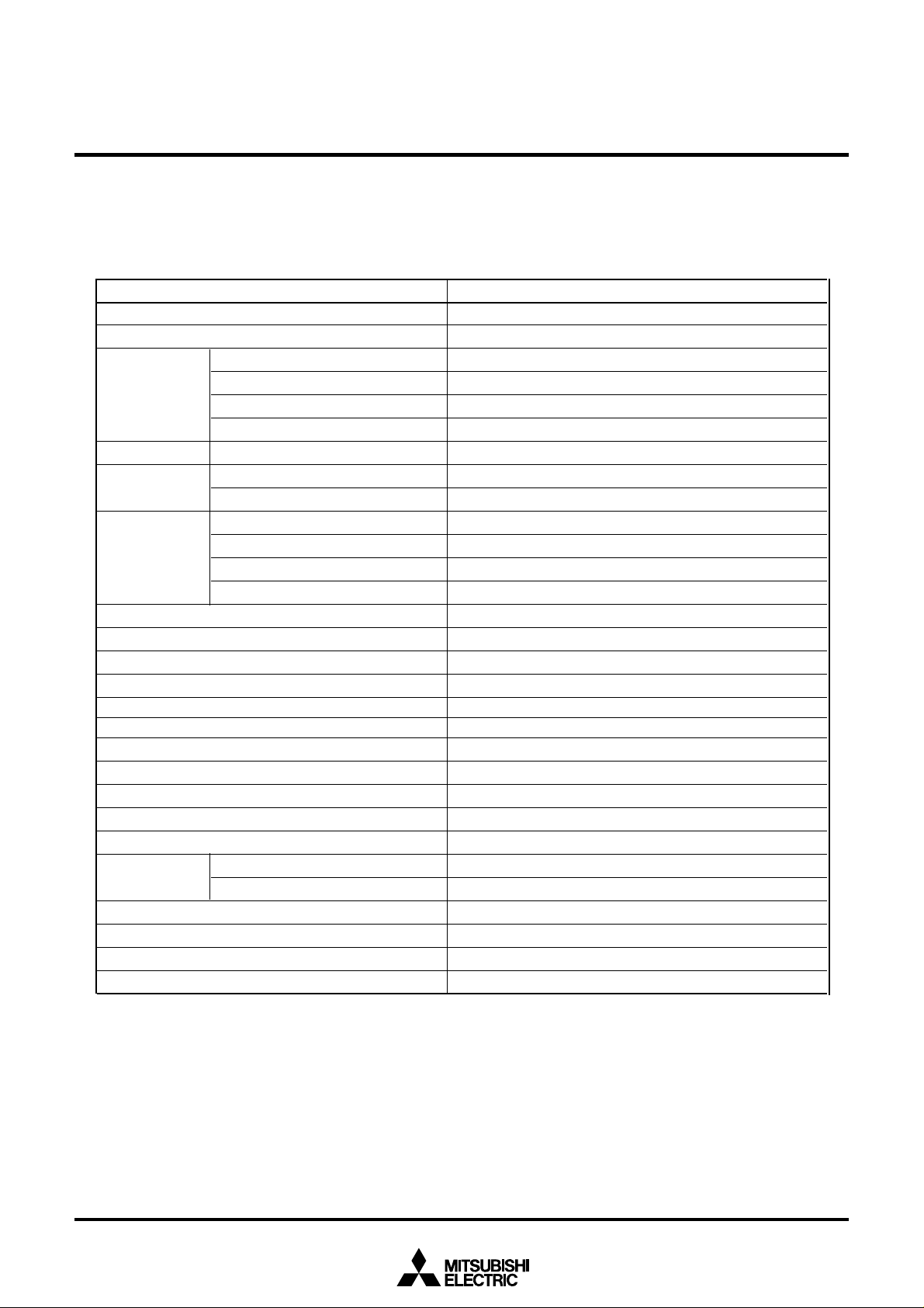
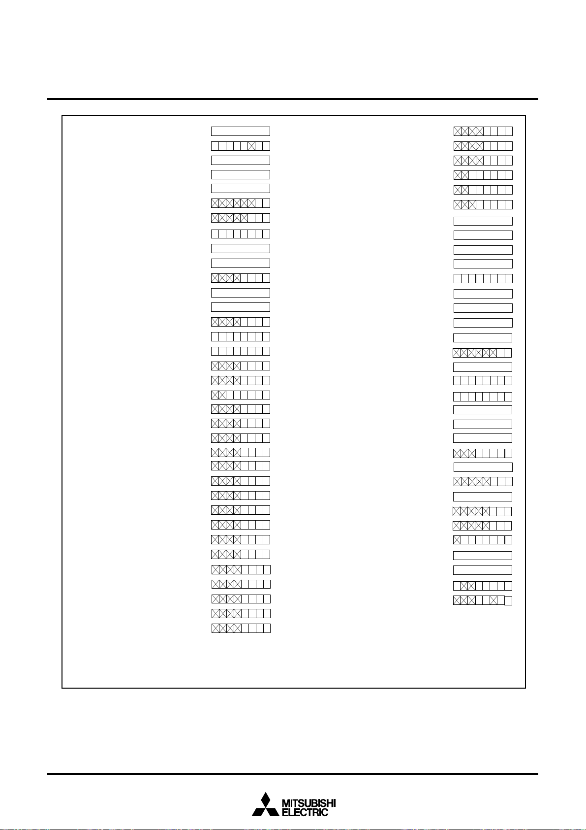
Table 1.5.3 Pin description (1)
MITSUBISHI MICROCOMPUTERS
M306V2ME-XXXFP
M306V2EEFP
and ON-SCREEN DISPLAY CONTROLLER
P i n n a m e
VC
C,
VS
S
C N VS
S
R E S E T
XI
N
U
XO
T
B Y T E
C C
A V
P 00 t o P 07
D0 t o D7
S i g n a l n a m e
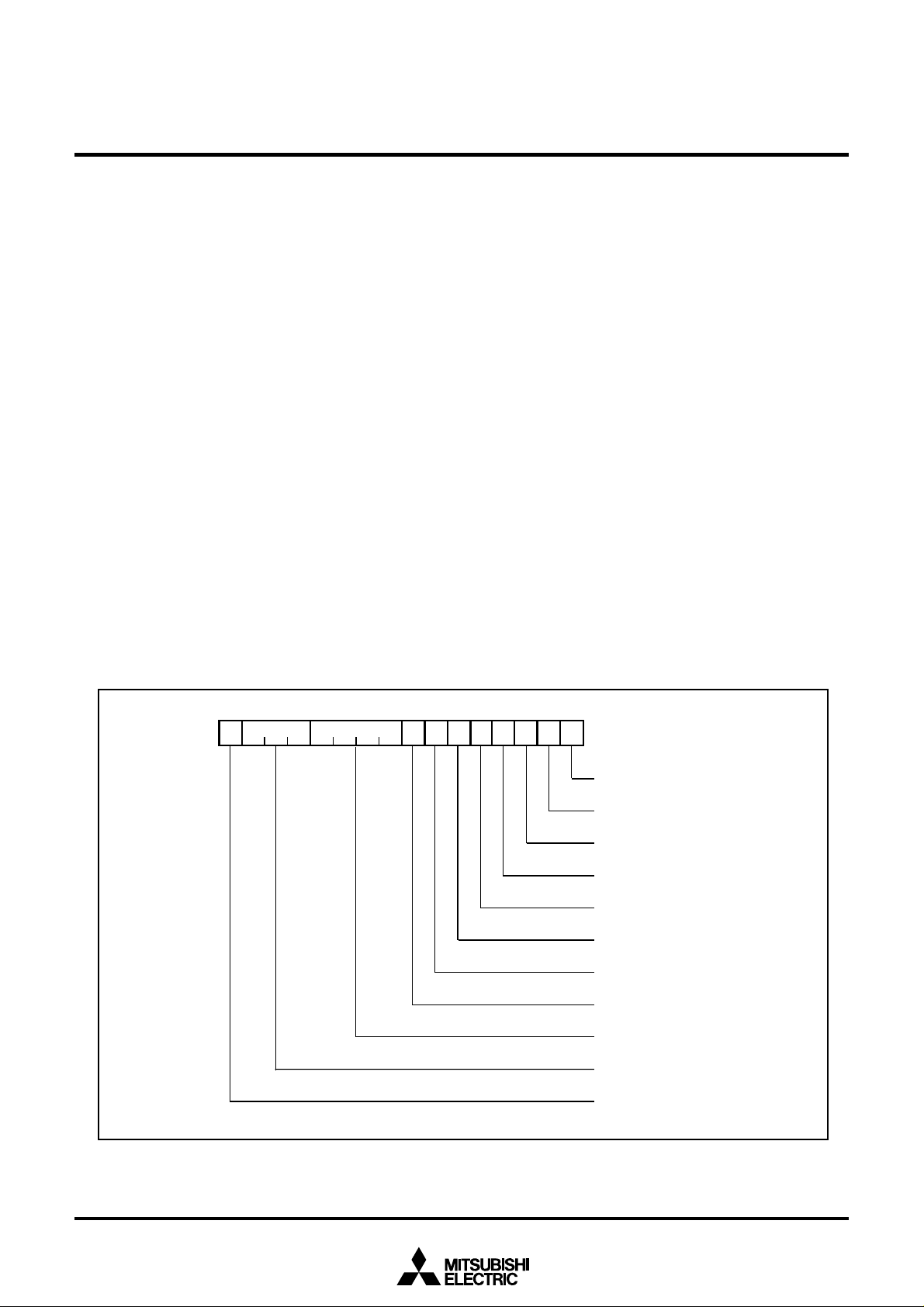
P o w e r s u p p l y
i n p u t
S S
C N V
R e s e t i n p u t
C l o c k i n p u t
C l o c k o u t p u t
E x t e r n a l d a t a
b u s w i d t h
s e l e c t i n p u t
A n a l o g p o w e r
s u p p l y i n p u t
I / O p o r t P 0
I / O t y p e
I n p u t
I n p u t
I n p u t
O u t p u t
I n p u t
I n p u t / o u t p u t
I n p u t / o u t p u t
F u n c t i o n
p i n . S u p p l y 0 V t o t h e
p i n
S u p p l y 4 . 5 V t o 5 . 5 V t o t h e V
p i n w h e n o p e r a t i n g i n s i n g l e - c h i p o r m e m o r y e x p a n s i o n m o d e .
p i n w h e n i n m i c r o p r o c e s s o r m o d e
T h i s p i n s w i t c h e s b e t w e e n p r o c e s s o r m o d e s . C o n n e c t i t t o t h e
S S
V
C o n n e c t i t t o t h e V
C C
C C
VS
.
S
.
A “ L ” o n t h i s i n p u t r e s e t s t h e m i c r o c o m p u t e r .
p i n o p e n
p i n a n d l e a v e t h e
a n d t h e
p i n s .
U
T h e s e p i n s a r e p r o v i d e d f o r t h e m a i n c l o c k g e n e r a t i n g c i r c u i t . C o n n e c t
a c e r a m i c r e s o n a t o r o r c r y s t a l b e t w e e n t h e X
u s e a n e x t e r n a l l y d e r i v e d c l o c k , i n p u t i t t o t h e X
X
O U T
.
I N
I N
XO
T
To
T h i s p i n s e l e c t s t h e w i d t h o f a n e x t e r n a l d a t a b u s . A 1 6 - b i t w i d t h i s
s e l e c t e d w h e n t h i s i n p u t i s “ L ” ; a n 8 - b i t w i d t h i s s e l e c t e d w h e n t h i s
i n p u t i s “ H ” . T h i s i n p u t m u s t b e f i x e d t o e i t h e r “ H ” o r “ L . ” W h e n
o p e r a t i n g i n s i n g l e - c h i p m o d e , c o n n e c t t h i s p i n t o V
S S.
T h i s p i n i s a p o w e r s u p p l y i n p u t f o r t h e A - D c o n v e r t e r . C o n n e c t t h i s
C C.
p i n t o V
T h i s i s a n 8 - b i t C M O S I / O p o r t . I t h a s a n i n p u t / o u t p u t p o r t d i r e c t i o n
r e g i s t e r t h a t a l l o w s t h e u s e r t o s e t e a c h p i n f o r i n p u t o r o u t p u t
i n d i v i d u a l l y . W h e n s e t f o r i n p u t i n s i n g l e - c h i p m o d e , t h e u s e r c a n s p e c i f y
i n u n i t s o f f o u r b i t s v i a s o f t w a r e w h e t h e r o r n o t t h e y a r e t i e d t o a p u l l - u p
r e s i s t o r . I n m e m o r y e x p a n s i o n a n d m i c r o p r o c e s s o r m o d e s , t h e u s e r
c a n n o t s p e c i f y t h a t .
W h e n s e t a s a s e p a r a t e b u s , t h e s e p i n s i n p u t a n d o u t p u t d a t a ( D
0–
D7) .
P 10 t o P 17 I / O p o r t P 1
t o
8
D1
D
P 20 t o P 27
5
I / O p o r t P 2
A0 t o A7
A0/ D0 t o
7/
A
o
A0
A1/ D0
P 30 t o P 37
A8 t o A1
t o
A8/ D7,
A
P 40 t o P 47
t o C
t o
C S
A
D7
t
A7/ D6
I / O p o r t P 3
5
9
A1
5
I / O p o r t P 4
0
S3,
1 6
A1
9
I n p u t / o u t p u t
I n p u t / o u t p u t
O u t p u t
I n p u t / o u t p u t
O u t p u t
I n p u t / o u t p u t
I n p u t / o u t p u t
O u t p u t
I n p u t / o u t p u t
O u t p u t
I n p u t / o u t p u t
O u t p u t
O u t p u t
T h i s i s a n 8 - b i t I / O p o r t e q u i v a l e n t t o P 0 . I n p u t / o u t p u t
W h e n s e t a s a s e p a r a t e b u s , t h e s e p i n s i n p u t a n d o u t p u t d a t a
( D8– D
T h i s i s a n 8 - b i t I / O p o r t e q u i v a l e n t t o P 0 .
T h e s e p i n s o u t p u t 8 l o w - o r d e r a d d r e s s b i t s ( A
I f t h e e x t e r n a l b u s i s s e t a s a n 8 - b i t w i d e m u l t i p l e x e d b u s , t h e s e p i n s
i n p u t a n d o u t p u t d a t a ( D
( A
0–
A7) s e p a r a t e d i n t i m e b y m u l t i p l e x i n g .
I f t h e e x t e r n a l b u s i s s e t a s a 1 6 - b i t w i d e m u l t i p l e x e d b u s , t h e s e p i n s
i n p u t a n d o u t p u t d a t a ( D
0–
D7) a n d o u t p u t 8 l o w - o r d e r a d d r e s s b i t s
0–
D6) a n d o u t p u t a d d r e s s ( A1– A7) s e p a r a t e d
i n t i m e b y m u l t i p l e x i n g . T h e y a l s o o u t p u t a d d r e s s ( A
0
– A7) .
0)
.
T h i s i s a n 8 - b i t I / O p o r t e q u i v a l e n t t o P 0 .
T h e s e p i n s o u t p u t 8 m i d d l e - o r d e r a d d r e s s b i t s ( A
a n d o u t p u t a d d r e s s (
I f t h e e x t e r n a l b u s i s s e t a s a 1 6 - b i t w i d e m u l t i p l e x e d b u s , t h e s e p i n s
i n p u t a n d o u t p u t d a t a ( D
7)
b y m u l t i p l e x i n g . T h e y a l s o o u t p u t a d d r e s s ( A
8–
A1
5)
.
A8) s e p a r a t e d i n t i m e
9–
A1
5)
.
T h i s i s a n 8 - b i t I / O p o r t e q u i v a l e n t t o P 0 .
a r e 4 h i g h -
C
T h e s e p i n s o u t p u t C S0– C S3 s i g n a l s a n d A1
s e l e c t s i g n a l s u s e d t o s p e c i f y a n a c c e s s s p a c e . A
6–
A1
9.
S0– C S3 a r e c h i p
1 6–
A1
9
o r d e r a d d r e s s b i t s .
1 5
) .
Rev. 1.0
7
MITSUBISHI MICROCOMPUTERS
M306V2ME-XXXFP
M306V2EEFP
SINGLE-CHIP 16-BIT CMOS MICROCOMPUTER with CLOSED CAPTION DECODER
and ON-SCREEN DISPLAY CONTROLLER
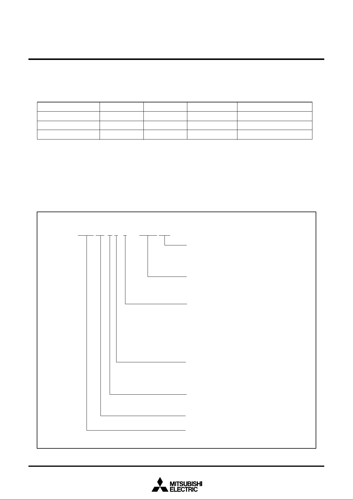
Table 1.5.4 Pin description (continued) (2)
S i g n a l n a m eF
P 50 t o P 5
7
W R L / W R ,
W R H / B H E ,
R D ,
B C L K ,
H L D A ,
H O L D ,
A L E ,
R D Y
P 60 t o P 63,
P 6
7
P 70 t o P 77
2
, P 83,
P 8
P 86, P 8
7
P 90 t o P 9
4
P 1 00 t o P 1 0
I / O p o r t P 5
I / O p o r t P 7
I / O p o r t P 8
I / O p o r t P 9
7
I / O p o r t P 1 0
I n p u t / o u t p u t
O u t p u t
O u t p u t
O u t p u t
O u t p u t
O u t p u t
I n p u t
O u t p u t
I n p u t
I n p u t / o u t p u tI / O p o r t P 6
I n p u t / o u t p u t
I n p u t / o u t p u t
I n p u t / o u t p u t
I n p u t / o u t p u t
T h i s i s a n 8 - b i t I / O p o r t e q u i v a l e n t t o P 0 . I n s i n g l e - c h i p m o d e , P 57 i n
t h i s p o r t o u t p u t s a d i v i d e - b y - 8 o r d i v i d e - b y - 3 2 c l o c k o f X
t h e s a m e f r e q u e n c y a s X
O u t p u t W R L , W R H ( W R a n d B H E ) , R D , B C L K , H L D A , a n d A L E
s i g n a l s . W R L a n d W R H , a n d B H E a n d W R c a n b e s w i t c h e d u s i n g
s o f t w a r e c o n t r o l .
■ W R L , W R H , a n d R D s e l e c t e d
W i t h a 1 6 - b i t e x t e r n a l d a t a b u s , d a t a i s w r i t t e n t o e v e n a d d r e s s e s
w h e n t h e W R L s i g n a l i s “ L ” a n d t o t h e o d d a d d r e s s e s w h e n t h e W R H
s i g n a l i s “ L ” . D a t a i s r e a d w h e n R D i s “ L ” .
■ W R , B H E , a n d R D s e l e c t e d
D a t a i s w r i t t e n w h e n W R i s “ L ” . D a t a i s r e a d w h e n R D i s “ L ” . O d d
a d d r e s s e s a r e a c c e s s e d w h e n B H E i s “ L ” . U s e t h i s m o d e w h e n u s i n g
a n 8 - b i t e x t e r n a l d a t a b u s .
W h i l e t h e i n p u t l e v e l a t t h e H O L D p i n i s “ L ” , t h e m i c r o c o m p u t e r i s
p l a c e d i n t h e h o l d s t a t e . W h i l e i n t h e h o l d s t a t e , H L D A o u t p u t s a “ L ”
l e v e l . A L E i s u s e d t o l a t c h t h e a d d r e s s . W h i l e t h e i n p u t l e v e l o f t h e
R D Y p i n i s “ L ” , t h e m i c r o c o m p u t e r i s i n t h e r e a d y s t a t e .
T h i s i s a n 5 - b i t I / O p o r t e q u i v a l e n t t o P 0 . W h e n s e t f o r i n p u t i n s i n g l e c h i p , m i c r o p r o c e s s o r a n d m e m o r y e x p a n s i o n m o d e s , t h e u s e r c a n
s p e c i f y i n u n i t s o f f o u r b i t s v i a s o f t w a r e w h e t h e r o r n o t t h e y a r e t i e d t o a
p u l l - u p r e s i s t o r . P i n s i n t h i s p o r t a l s o f u n c t i o n a s U A R T 0 , U A R T 2 a n d
m u l t i - m a s t e r I
T h i s i s a n 8 - b i t I / O p o r t e q u i v a l e n t t o P 6 ( P 70 a n d P 71 a r e N - c h a n n e l
o p e n - d r a i n o u t p u t ) . P i n s i n t h i s p o r t a l s o f u n c t i o n a s t i m e r s A 2 a n d A 3 ,
U A R T 2 , m u l t i - m a s t e r I
s e l e c t e d b y s o f t w a r e .
P 82, P 83, P 86 a n d P 87 a r e I / O p o r t s w i t h t h e s a m e f u n c t i o n s a s P 6 .
U s i n g s o f t w a r e , P 82 a n d P 83 c a n b e m a d e t o f u n c t i o n a s t h e I / O p i n s f o r
t h e i n p u t p i n s f o r e x t e r n a l i n t e r r u p t s . P 8
s o f t w a r e t o f u n c t i o n a s t h e I / O p i n s f o r a s u b - c l o c k g e n e r a t i o n c i r c u i t . I n
t h i s c a s e , c o n n e c t a q u a r t z o s c i l l a t o r b e t w e e n P 8
( X
T h i s i s a n 5 - b i t I / O p o r t e q u i v a l e n t t o P 6 . P i n s i n t h i s p o r t a l s o f u n c t i o n
a s T i m e r B 0 t o B 2 i n p u t p i n s , D - A c o n v e r t e r o u t p u t p i n s , o r m u l t i - m a s t e r
2
I
T h i s i s a n 8 - b i t I / O p o r t e q u i v a l e n t t o P 6 . P i n s i n t h i s p o r t a l s o f u n c t i o n
a s A - D c o n v e r t e r i n p u t p i n s . F u r t h e r m o r e , P 1 0
a s i n p u t p i n s f o r O S D f u n c t i o n .
C I N
2
C - B U S i n t e r f a c e 0 I / O p i n s a s s e l e c t e d b y s o f t w a r e .
2
C - B U S i n t e r f a c e 0 , o r H
C I N
p i n ) .
C - B U S i n t e r f a c e 1 I / O p i n s .
u n c t i o
nP i n n a m e I / O t y p e
a s s e l e c t e d b y s o f t w a r e .
S Y N C
6
a n d P 87 c a n b e s e t u s i n g
6
( X
0
a n d P 1 01 a l s o f u n c t i o n
I N
o r a c l o c k o f
c o u n t e r I / O p i n s a s
C O U T
p i n ) a n d P 87
R , G , B
O U T 1 , O U T 2
O S C 1
O S C 2
C V
V
H L F
T V S E T B
8
I N
H O L D
O S D o u t p u t
O u t p u t
O S D o u t p u tO u t p u t
C l o c k i n p u t
I n p u t
f o r O S D
C l o c k o u t p u t
O u t p u t
f o r O S D
I / O f o r d a t a
I n p u t
s l i c e r
I n p u t
I n p u t / o u t p u t
T e s t i n p u t
I n p u t
T h e s e a r e O S D o u t p u t p i n s ( a n a l o g o u t p u t ) .
T h e s e a r e O S D o u t p u t p i n s ( d i g i t a l o u t p u t ) .
T h i s i s a n O S D c l o c k i n p u t p i n .
T h i s i s a n O S D c l o c k o u t p u t p i n .
I n p u t c o m p o s i t e v i d e o s i g n a l t h r o u g h a c a p a c i t o r .
C o n n e c t a c a p a c i t o r b e t w e e n V
H O L D
a n d V s s .
C o n n e c t a f i l t e r u s i n g o f a c a p a c i t o r a n d a r e s i s t o r
b e t w e e n H L F a n d V s s .
T h i s i s a t e s t i n p u t p i n . F i x i t t o “ L . ”
Rev. 1.0

MITSUBISHI MICROCOMPUTERS
M306V2ME-XXXFP
M306V2EEFP
SINGLE-CHIP 16-BIT CMOS MICROCOMPUTER with CLOSED CAPTION DECODER
and ON-SCREEN DISPLAY CONTROLLER
2. OPERATION OF FUNCTIONAL BLOKS
This microcomputer accommodates certain units in a single chip. These units include ROM and RAM to
store instructions and data and the central processing unit (CPU) to execute arithmetic/logic operations.
Also included are peripheral units such as timers, serial I/O, D-A converter, DMAC, OSD circuit, data slicer,
A-D converter, and I/O ports.
The following explains each unit.
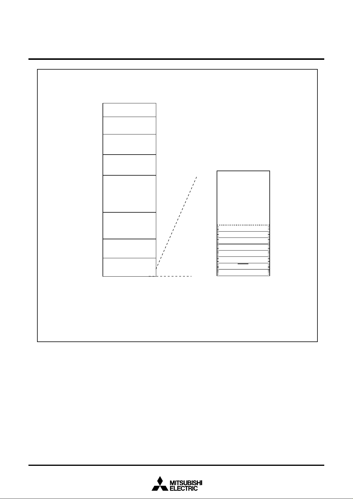
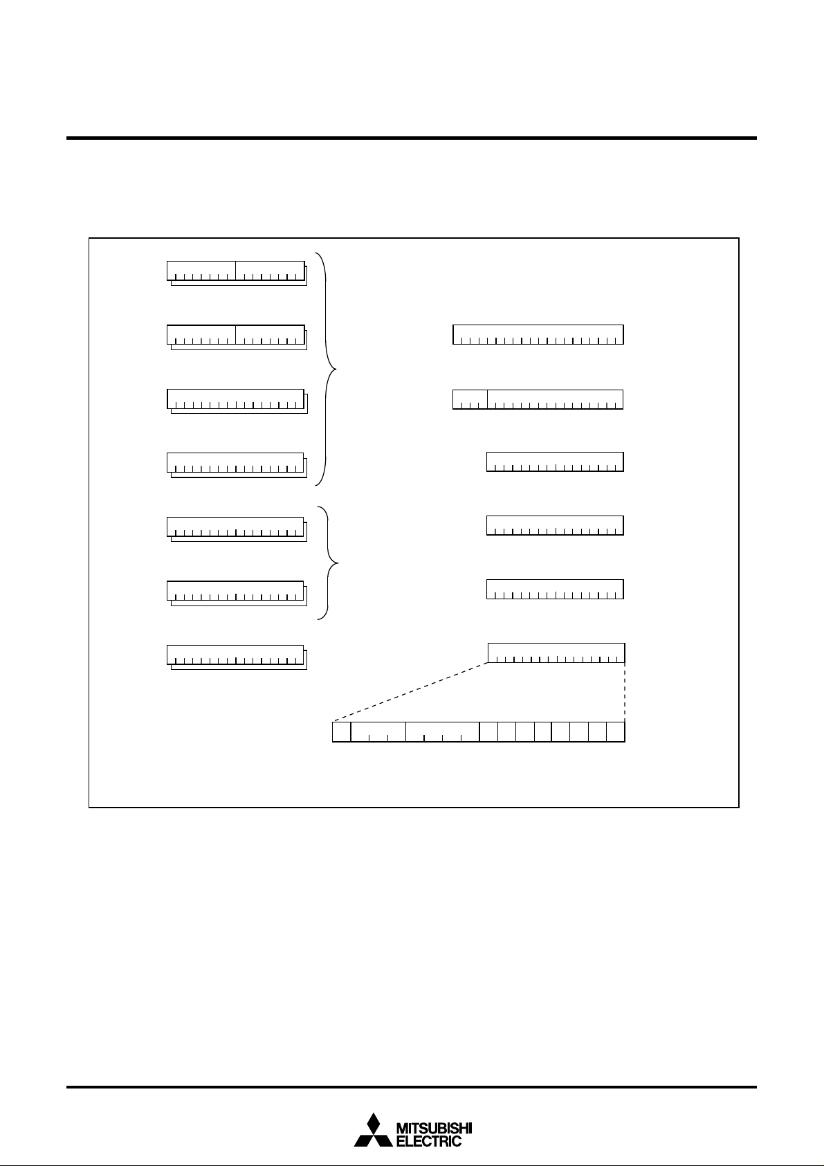
2.1 Memory
Figure 2.1.1 is a memory map. The address space extends the 1M bytes from address 0000016 to
FFFFF16. From FFFFF16 down is ROM. There is 192K bytes of internal ROM from D000016 to FFFFF16.
The vector table for fixed interrupts such as the reset mapped to FFFDC16 to FFFFF16. The starting address of the interrupt routine is stored here. The address of the vector table for timer interrupts, etc., can be
set as desired using the internal register (INTB). See the section on interrupts for details.
5K bytes of internal RAM is mapped to the space from 02C0016 to 03FFF16. In addition to storing data, the
RAM also stores the stack used when calling subroutines and when interrupts are generated.
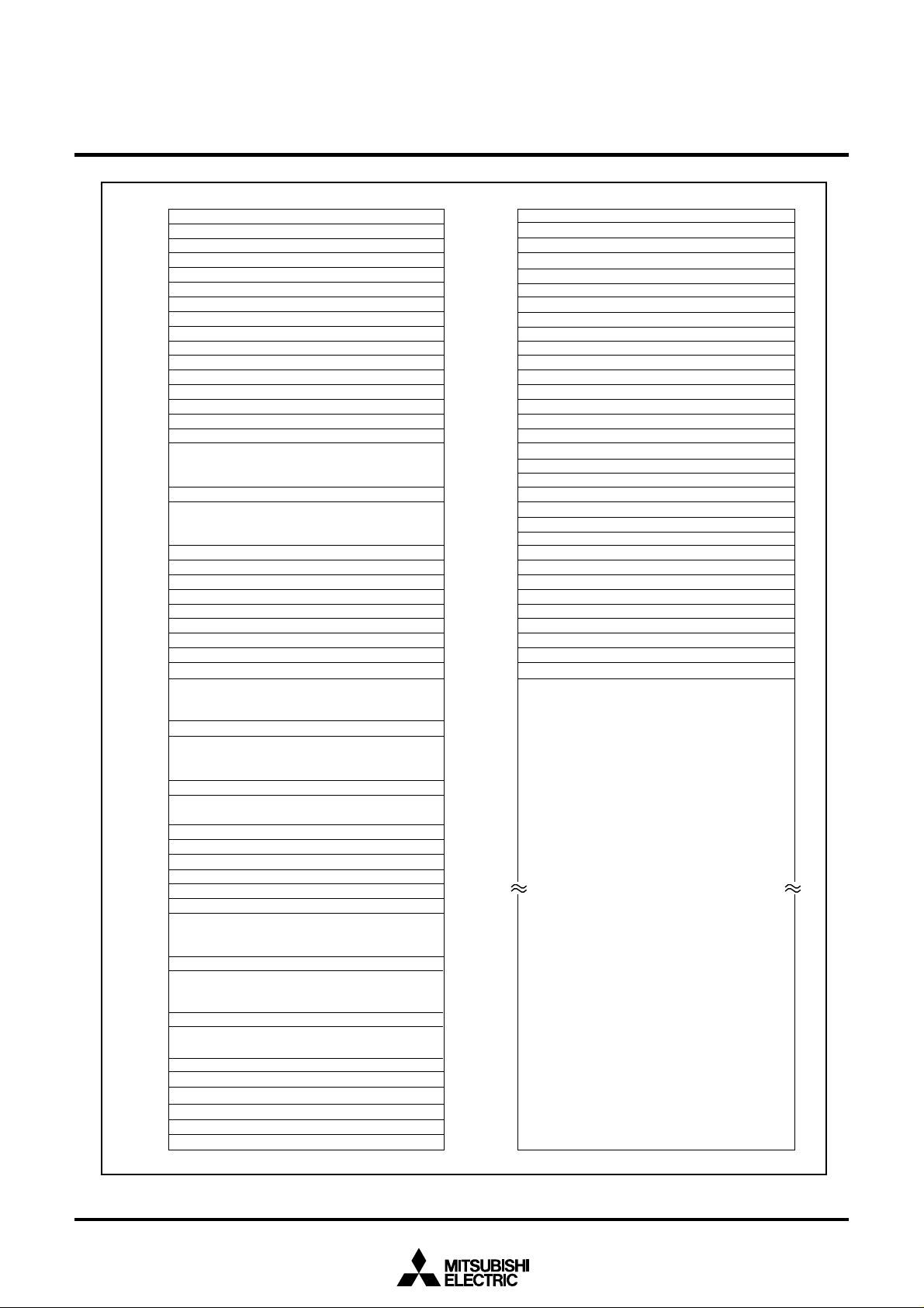
The SFR area is mapped to 0000016 to 003FF16. This area accommodates the control registers for peripheral devices such as I/O ports, A-D converter, serial I/O, and timers, etc. Figures 2.1.2 to 2.1.5 are location
of peripheral unit control registers. Any part of the SFR area that is not occupied is reserved and cannot be
used for other purposes.
The special page vector table is mapped to FFE0016 to FFFDB16. If the starting addresses of subroutines
or the destination addresses of jumps are stored here, subroutine call instructions and jump instructions
can be used as 2-byte instructions, reducing the number of program steps.
In memory expansion mode and microprocessor mode, a part of the spaces are reserved and cannot be
used. The following spaces cannot be used.
• The space between 0100016 and 02BFF16 (in memory expansion and microprocessor modes)
• The space between B000016 and CFFFF16 (in memory expansion mode)
Rev. 1.0
9
00000
003FF
00400
013FF
01400
02BFF
02C00
03FFF
04000
SINGLE-CHIP 16-BIT CMOS MICROCOMPUTER with CLOSED CAPTION DECODER
16
16
16
SFR area
(Refer to Figures 2.1.2 to 2.1.5)
OSD RAM area
16
16
Internal reserved
area (See note 1)
16
16
Internal RAM area
16
16
FFE00
MITSUBISHI MICROCOMPUTERS
M306V2ME-XXXFP
M306V2EEFP
and ON-SCREEN DISPLAY CONTROLLER
16
8FFFF
16
90000
16
AFFFF
16
B0000
16
CFFFF
16
D0000
16
FFFFF
16
Notes 1: During memory expansion and microprocessor modes, cannot be used.
2: During memory expansion mode, cannot be used.
Figure 2.1.1 Memory map
External area
OSD ROM area
Internal reserved
area (See note 2)
Internal ROM area
FFFDC
FFFFF
Special page
vector table
16
Undefined instruction
Overflow
BRK instruction
Address match
Single step
Watchdog timer
16
DBC
Reset
10
Rev. 1.0
SINGLE-CHIP 16-BIT CMOS MICROCOMPUTER with CLOSED CAPTION DECODER
0 0 0 01
6
0 0 0 11
6
0 0 0 21
6
0 0 0 31
6
0 0 0 41
6
P r o c e s s o r m o d e r e g i s t e r 0 ( P M 0 )
0 0 0 51
6
P r o c e s s o r m o d e r e g i s t e r 1 ( P M 1 )
0 0 0 61
6
S y s t e m c l o c k c o n t r o l r e g i s t e r 0 ( C M 0 )
0 0 0 71
6
S y s t e m c l o c k c o n t r o l r e g i s t e r 1 ( C M 1 )
0 0 0 81
6
C h i p s e l e c t c o n t r o l r e g i s t e r ( C S R )
0 0 0 91
6
A d d r e s s m a t c h i n t e r r u p t e n a b l e r e g i s t e r ( A I E R )
0 0 0 A1
6
P r o t e c t r e g i s t e r ( P R C R )
0 0 0 B1
6
0 0 0 C1
6
0 0 0 D1
6
0 0 0 E1
6
W a t c h d o g t i m e r s t a r t r e g i s t e r ( W D T S )
0 0 0 F1
6
W a t c h d o g t i m e r c o n t r o l r e g i s t e r ( W D C )
0 0 1 01
6
0 0 1 11
6
A d d r e s s m a t c h i n t e r r u p t r e g i s t e r 0 ( R M A D 0 )
0 0 1 21
6
0 0 1 31
6
0 0 1 41
6
A d d r e s s m a t c h i n t e r r u p t r e g i s t e r 1 ( R M A D 1 )
0 0 1 51
6
0 0 1 61
6
0 0 1 71
6
0 0 1 81
6
0 0 1 91
6
0 0 1 A1
6
0 0 1 B1
6
0 0 1 C1
6
0 0 1 D1
6
0 0 1 E1
6
0 0 1 F1
6
0 0 2 01
6
0 0 2 11
6
D M A 0 s o u r c e p o i n t e r ( S A R 0 )
0 0 2 21
6
0 0 2 31
6
0 0 2 41
6
0 0 2 51
6
D M A 0 d e s t i n a t i o n p o i n t e r ( D A R 0 )
0 0 2 61
6
0 0 2 71
6
0 0 2 81
6
D M A 0 t r a n s f e r c o u n t e r ( T C R 0 )
0 0 2 91
6
0 0 2 A1
6
0 0 2 B1
6
0 0 2 C1
6
D M A 0 c o n t r o l r e g i s t e r ( D M 0 C O N )
0 0 2 D1
6
0 0 2 E1
6
0 0 2 F1
6
0 0 3 01
6
0 0 3 11
6
D M A 1 s o u r c e p o i n t e r ( S A R 1 )
0 0 3 21
6
0 0 3 31
6
0 0 3 41
6
D M A 1 d e s t i n a t i o n p o i n t e r ( D A R 1 )
0 0 3 51
6
0 0 3 61
6
0 0 3 71
6
0 0 3 81
6
D M A 1 t r a n s f e r c o u n t e r ( T C R 1 )
0 0 3 91
6
0 0 3 A1
6
0 0 3 B1
6
0 0 3 C1
6
D M A 1 c o n t r o l r e g i s t e r ( D M 1 C O N )
0 0 3 D1
6
0 0 3 E1
6
0 0 3 F1
6
MITSUBISHI MICROCOMPUTERS
M306V2ME-XXXFP
M306V2EEFP
and ON-SCREEN DISPLAY CONTROLLER
0 0 4 01
6
0 0 4 11
6
0 0 4 21
6
0 0 4 31
6
0 0 4 41
6
O S D 1 i n t e r r u p t c o n t r o l r e g i s t e r ( O S D 1 I C )
0 0 4 51
6
I n t e r r u p t c o n t r o l r e s e r v e d r e g i s t e r 0 ( R E 0 I C )
0 0 4 61
6
I n t e r r u p t c o n t r o l r e s e r v e d r e g i s t e r 1 ( R E 1 I C )
0 0 4 71
6
I n t e r r u p t c o n t r o l r e s e r v e d r e g i s t e r 2 ( R E 2 I C )
0 0 4 81
6
O S D 2 i n t e r r u p t c o n t r o l r e g i s t e r ( O S D 2 I C )
0 0 4 91
6
M u l t i - m a s t e r I2C - B U S i n t e r f a c e 1 i n t e r r u p t c o n t r o l r e g i s t e r ( I I C 1 I C )
0 0 4 A1
6
B u s c o l l i s i o n d e t e c t i o n i n t e r r u p t c o n t r o l r e g i s t e r ( B C N I C )
0 0 4 B1
6
D M A 0 i n t e r r u p t c o n t r o l r e g i s t e r ( D M 0 I C )
0 0 4 C1
6
D M A 1 i n t e r r u p t c o n t r o l r e g i s t e r ( D M 1 I C )
0 0 4 D1
6
M u l t i - m a s t e r I2C - B U S i n t e r f a c e 0 i n t e r r u p t c o n t r o l r e g i s t e r ( I I C 0 I C )
0 0 4 E1
6
A - D c o n v e r s i o n i n t e r r u p t c o n t r o l r e g i s t e r ( A D I C )
0 0 4 F1
6
U A R T 2 t r a n s m i t i n t e r r u p t c o n t r o l r e g i s t e r ( S 2 T I C )
0 0 5 01
6
U A R T 2 r e c e i v e i n t e r r u p t c o n t r o l r e g i s t e r ( S 2 R I C )
0 0 5 11
6
U A R T 0 t r a n s m i t i n t e r r u p t c o n t r o l r e g i s t e r ( S 0 T I C )
0 0 5 21
6
U A R T 0 r e c e i v e i n t e r r u p t c o n t r o l r e g i s t e r ( S 0 R I C )
0 0 5 31
6
D a t a s l i c e r i n t e r r u p t c o n t r o l r e g i s t e r ( D S I C )
i n t e r r u p t c o n t r o l r e g i s t e r ( V S Y N C I C
0 0 5 41
6
V
0 0 5 51
0 0 5 61
0 0 5 71
0 0 5 81
0 0 5 91
0 0 5 A1
0 0 5 B1
0 0 5 C1
0 0 5 D1
0 0 5 E1
0 0 5 F1
0 0 6 01
0 1 F F1
S Y N C
6
T i m e r A 0 i n t e r r u p t c o n t r o l r e g i s t e r ( T A 0 I C )
6
T i m e r A 1 i n t e r r u p t c o n t r o l r e g i s t e r ( T A 1 I C )
6
T i m e r A 2 i n t e r r u p t c o n t r o l r e g i s t e r ( T A 2 I C )
6
T i m e r A 3 i n t e r r u p t c o n t r o l r e g i s t e r ( T A 3 I C )
6
T i m e r A 4 i n t e r r u p t c o n t r o l r e g i s t e r ( T A 4 I C )
6
T i m e r B 0 i n t e r r u p t c o n t r o l r e g i s t e r ( T B 0 I C )
6
T i m e r B 1 i n t e r r u p t c o n t r o l r e g i s t e r ( T B 1 I C )
6
T i m e r B 2 i n t e r r u p t c o n t r o l r e g i s t e r ( T B 2 I C )
6
I N T 0 i n t e r r u p t c o n t r o l r e g i s t e r ( I N T 0 I C )
6
I N T 1 i n t e r r u p t c o n t r o l r e g i s t e r ( I N T 1 I C )
6
I n t e r r u p t c o n t r o l r e s e r v e d r e g i s t e r 3 ( R E 3 I C )
6
6
)
Figure 2.1.2 Location of peripheral unit control registers (1)
Rev. 1.0
11
0 2 0 0
1 6
0 2 0 1
1 6
S P R I T E O S D c o n t r o l r e g i s t e r ( S C )
0 2 0 2
1 6
O S D c o n t r o l r e g i s t e r 1 ( O C 1 )
0 2 0 3
1 6
O S D c o n t r o l r e g i s t e r 2 ( O C 2 )
0 2 0 4
1 6
H o r i z o n t a l p o s i t i o n r e g i s t e r ( H P )
0 2 0 5
1 6
C l o c k c o n t r o l r e g i s t e r ( C S )
0 2 0 6
1 6
I / O p o l a r i t y c o n t r o l r e g i s t e r ( P C )
0 2 0 7
1 6
O S D c o n t r o l r e g i s t e r 3 ( O C 3 )
0 2 0 8
1 6
R a s t e r c o l o r r e g i s t e r ( R S C )
0 2 0 9
1 6
0 2 0 A
1 6
0 2 0 B
1 6
0 2 0 C
1 6
T o p b o r d e r c o n t r o l r e g i s t e r ( T B R )
0 2 0 D
1 6
0 2 0 E
1 6
B o t t o m b o r d e r c o n t r o l r e g i s t e r ( B B R )
0 2 0 F
1 6
0 2 1 0
1 6
B l o c k c o n t r o l r e g i s t e r 1 ( B C 1)
0 2 1 1
1 6
B l o c k c o n t r o l r e g i s t e r 2 ( B C 2)
0 2 1 2
1 6
B l o c k c o n t r o l r e g i s t e r 3 ( B C 3)
0 2 1 3
1 6
B l o c k c o n t r o l r e g i s t e r 4 ( B C 4)
0 2 1 4
1 6
B l o c k c o n t r o l r e g i s t e r 5 ( B C 5)
0 2 1 5
1 6
B l o c k c o n t r o l r e g i s t e r 6 ( B C 6)
0 2 1 6
1 6
B l o c k c o n t r o l r e g i s t e r 7 ( B C 7)
0 2 1 7
1 6
B l o c k c o n t r o l r e g i s t e r 8 ( B C 8)
0 2 1 8
1 6
B l o c k c o n t r o l r e g i s t e r 9 ( B C 9)
0 2 1 9
1 6
B l o c k c o n t r o l r e g i s t e r 1 0 ( B C 1 0)
0 2 1 A
1 6
B l o c k c o n t r o l r e g i s t e r 1 1 ( B C 1 1)
0 2 1 B
1 6
B l o c k c o n t r o l r e g i s t e r 1 2 ( B C 1 2)
0 2 1 C
1 6
B l o c k c o n t r o l r e g i s t e r 1 3 ( B C 1 3)
0 2 1 D
1 6
B l o c k c o n t r o l r e g i s t e r 1 4 ( B C 1 4)
0 2 1 E
1 6
B l o c k c o n t r o l r e g i s t e r 1 5 ( B C 1 5)
0 2 1 F
1 6
B l o c k c o n t r o l r e g i s t e r 1 6 ( B C 1 6)
0 2 2 0
1 6
V e r t i c a l p o s i t i o n r e g i s t e r 1 ( V P 1 )
0 2 2 1
1 6
0 2 2 2
1 6
V e r t i c a l p o s i t i o n r e g i s t e r 2 ( V P 2 )
0 2 2 3
1 6
0 2 2 4
1 6
V e r t i c a l p o s i t i o n r e g i s t e r 3 ( V P 3 )
0 2 2 5
1 6
0 2 2 6
1 6
V e r t i c a l p o s i t i o n r e g i s t e r 4 ( V P 4 )
0 2 2 7
1 6
0 2 2 8
1 6
V e r t i c a l p o s i t i o n r e g i s t e r 5 ( V P 5 )
0 2 2 9
1 6
0 2 2 A
1 6
V e r t i c a l p o s i t i o n r e g i s t e r 6 ( V P 6 )
0 2 2 B
1 6
0 2 2 C
1 6
V e r t i c a l p o s i t i o n r e g i s t e r 7 ( V P 7 )
0 2 2 D
1 6
0 2 2 E
1 6
V e r t i c a l p o s i t i o n r e g i s t e r 8 ( V P 8 )
0 2 2 F
1 6
0 2 3 0
1 6
V e r t i c a l p o s i t i o n r e g i s t e r 9 ( V P 9 )
0 2 3 1
1 6
0 2 3 2
1 6
V e r t i c a l p o s i t i o n r e g i s t e r 1 0 ( V P 1 0 )
0 2 3 3
1 6
0 2 3 4
1 6
V e r t i c a l p o s i t i o n r e g i s t e r 1 1 ( V P 1 1 )
0 2 3 5
1 6
0 2 3 6
1 6
V e r t i c a l p o s i t i o n r e g i s t e r 1 2 ( V P 1 2 )
0 2 3 7
1 6
0 2 3 8
1 6
V e r t i c a l p o s i t i o n r e g i s t e r 1 3 ( V P 1 3 )
0 2 3 9
1 6
0 2 3 A
1 6
V e r t i c a l p o s i t i o n r e g i s t e r 1 4 ( V P 1 4 )
0 2 3 B
1 6
0 2 3 C
1 6
V e r t i c a l p o s i t i o n r e g i s t e r 1 5 ( V P 1 5 )
0 2 3 D
1 6
0 2 3 E
1 6
V e r t i c a l p o s i t i o n r e g i s t e r 1 6 ( V P 1 6 )
0 2 3 F
1 6
MITSUBISHI MICROCOMPUTERS
M306V2ME-XXXFP
M306V2EEFP
SINGLE-CHIP 16-BIT CMOS MICROCOMPUTER with CLOSED CAPTION DECODER
and ON-SCREEN DISPLAY CONTROLLER
0 2 4 0
1 6
C o l o r p a l e t t e r e g i s t e r 1 ( C R 1 )
0 2 4 1
1 6
0 2 4 2
1 6
C o l o r p a l e t t e r e g i s t e r 2 ( C R 2 )
0 2 4 3
1 6
0 2 4 4
1 6
C o l o r p a l e t t e r e g i s t e r 3 ( C R 3 )
0 2 4 5
1 6
0 2 4 6
1 6
C o l o r p a l e t t e r e g i s t e r 4 ( C R 4 )
0 2 4 7
1 6
0 2 4 8
1 6
C o l o r p a l e t t e r e g i s t e r 5 ( C R 5 )
0 2 4 9
1 6
0 2 4 A
1 6
C o l o r p a l e t t e r e g i s t e r 6 ( C R 6 )
0 2 4 B
1 6
0 2 4 C
1 6
C o l o r p a l e t t e r e g i s t e r 7 ( C R 7 )
0 2 4 D
1 6
0 2 4 E
1 6
C o l o r p a l e t t e r e g i s t e r 9 ( C R 9 )
0 2 4 F
1 6
0 2 5 0
1 6
C o l o r p a l e t t e r e g i s t e r 1 0 ( C R 1 0 )
0 2 5 1
1 6
0 2 5 2
1 6
C o l o r p a l e t t e r e g i s t e r 1 1 ( C R 1 1 )
0 2 5 3
1 6
0 2 5 4
1 6
C o l o r p a l e t t e r e g i s t e r 1 2 ( C R 1 2 )
0 2 5 5
1 6
0 2 5 6
1 6
C o l o r p a l e t t e r e g i s t e r 1 3 ( C R 1 3 )
0 2 5 7
1 6
0 2 5 8
1 6
C o l o r p a l e t t e r e g i s t e r 1 4 ( C R 1 4 )
0 2 5 9
1 6
0 2 5 A
1 6
C o l o r p a l e t t e r e g i s t e r 1 5 ( C R 1 5 )
0 2 5 B
1 6
0 2 5 C
1 6
0 2 5 D
1 6
O S D r e s e r v e d r e g i s t e r 1 ( O R 1 )
0 2 5 E
1 6
0 2 5 F
1 6
O S D c o n t r o l r e g i s t e r 4 ( O C 4 )
0 2 6 0
1 6
D a t a s l i c e r c o n t r o l r e g i s t e r 1 ( D S C 1 )
0 2 6 1
1 6
D a t a s l i c e r c o n t r o l r e g i s t e r 2 ( D S C 2 )
0 2 6 2
1 6
C a p t i o n d a t a r e g i s t e r 1 ( C D 1 )
0 2 6 3
1 6
0 2 6 4
1 6
C a p t i o n d a t a r e g i s t e r 2 ( C D 2 )
0 2 6 5
1 6
0 2 6 6
1 6
C a p t i o n p o s i t i o n r e g i s t e r ( C P S )
0 2 6 7
1 6
D a t a s l i c e r r e s e r v e d r e g i s t e r 2 ( D R 2 )
0 2 6 8
1 6
D a t a s l i c e r r e s e r v e d r e g i s t e r 1 ( D R 1 )
0 2 6 9
1 6
C l o c k r u n - i n d e t e c t r e g i s t e r ( C R D )
0 2 6 A
1 6
D a t a c l o c k p o s i t i o n r e g i s t e r ( D P S )
0 2 6 B
1 6
0 2 6 F
1 6
0 2 7 0
1 6
L e f t b o r d e r c o n t r o l r e g i s t e r ( L B R )
0 2 7 1
1 6
0 2 7 2
1 6
R i g h t b o r d e r c o n t r o l r e g i s t e r ( R B R )
0 2 7 3
1 6
0 2 7 4
1 6
S P R I T E v e r t i c a l p o s i t i o n r e g i s t e r 1 ( V S 1 )
0 2 7 5
1 6
0 2 7 6
1 6
S P R I T E v e r t i c a l p o s i t i o n r e g i s t e r 2 ( V S 2 )
0 2 7 7
1 6
0 2 7 8
1 6
S P R I T E h o r i z o n t a l p o s i t i o n r e g i s t e r ( H S )
0 2 7 9
1 6
0 2 7 A
1 6
O S D r e s e r v e d r e g i s t e r 4 ( O R 4 )
0 2 7 B
1 6
O S D r e s e r v e d r e g i s t e r 3 ( O R 3 )
0 2 7 C
1 6
O S D r e s e r v e d r e g i s t e r 2 ( O R 2 )
0 2 7 D
1 6
P e r i p h e r a l m o d e r e g i s t e r ( P M )
0 2 7 E
1 6
H
S Y N C
0 2 7 F
0 2 8 0
0 2 D F
1 6
1 6
1 6
c o u n t e r r e g i s t e r ( H C )
H
S Y N C
c o u n t e r l a t c h
Figure 2.1.3 Location of peripheral unit control registers (2)
12
Rev. 1.0
MITSUBISHI MICROCOMPUTERS
M306V2ME-XXXFP
M306V2EEFP
SINGLE-CHIP 16-BIT CMOS MICROCOMPUTER with CLOSED CAPTION DECODER
and ON-SCREEN DISPLAY CONTROLLER
02E0
02E1
02E2
02E3
02E4
02E5
02E6
02E7
02E8
02E9
02EA
02EB
02EC
02ED
02EE
02EF
0339
0340
0341
0342
0343
0344
0345
0346
0347
0348
0349
035E
035F
0360
0361
0362
0363
0364
0365
0366
0367
0368
0369
036A
036B
036C
036D
036E
036F
0370
0371
0372
0373
0374
0375
0376
0377
0378
0379
037A
037B
037C
037D
037E
037F
2
I
C0 data shift register (IIC0S0)
16
2
I
C0 address register (IIC0S0D)
16
2
16
I
C0 status register (IIC0S1)
2
16
C0 control register (IIC0S1D)
I
2
16
I
C0 clock control register (IIC0S2)
2
16
C0 port selection register (IIC0S2D)
I
2
16
C0 transmit buffer register (IIC0S0S)
I
16
2
16
I
C1 data shift register (IIC1S0)
2
16
I
C1 address register (IIC1S0D)
16
I2C1 status register (IIC1S1)
2
16
C1 control register (IIC1S1D)
I
2
I
C1 clock control register (IIC1S2)
16
2
16
C1 port selection register (IIC1S2D)
I
2
16
C1 transmit buffer register (IIC1S0S)
I
16
16
16
Reserved register 1 (INVC1)
16
16
16
16
16
16
16
Reserved register 0 (INVC0)
16
16
16
Interrupt request cause select register (IFSR)
16
16
16
Reserved register 3 (INVC3)
16
16
16
16
Reserved register 4 (INVC4)
16
16
16
16
16
16
16
16
16
16
16
16
16
16
16
16
Reserved register 5 (INVC5)
16
UART2 special mode register (U2SMR)
16
UART2 transmit/receive mode register (U2MR)
16
16
UART2 bit rate generator (U2BRG)
16
UART2 transmit buffer register (U2TB)
16
16
UART2 transmit/receive control register 0 (U2C0)
16
UART2 transmit/receive control register 1 (U2C1)
16
UART2 receive buffer register (U2RB)
16
0380
0381
0382
0383
0384
0385
0386
0387
0388
0389
038A
038B
038C
038D
038E
038F
0390
0391
0392
0393
0394
0395
0396
0397
0398
0399
039A
039B
039C
039D
039E
039F
03A0
03A1
03A2
03A3
03A4
03A5
03A6
03A7
03A8
03A9
03AA
03AB
03AC
03AD
03AE
03AF
03B0
03B1
03B2
03B3
03B4
03B5
03B6
03B7
03B8
03B9
03BA
03BB
03BC
03BD
03BE
03BF
16
Count start flag (TABSR)
16
Clock prescaler reset flag (CPSRF)
16
One-shot start flag (ONSF)
16
Trigger select register (TRGSR)
16
Up-down flag (UDF)
16
16
Timer A0 register (TA0)
16
16
Timer A1 register (TA1)
16
16
Timer A2 register (TA2)
16
16
Timer A3 register (TA3)
16
16
Timer A4 register (TA4)
16
16
Timer B0 register (TB0)
16
16
Timer B1 register (TB1)
16
16
Timer B2 register (TB2)
16
16
Timer A0 mode register (TA0MR)
16
Timer A1 mode register (TA1MR)
16
Timer A2 mode register (TA2MR)
16
Timer A3 mode register (TA3MR)
16
Timer A4 mode register (TA4MR)
16
Timer B0 mode register (TB0MR)
16
Timer B1 mode register (TB1MR)
Timer B2 mode register (TB2MR)
16
16
16
16
UART0 transmit/receive mode register (U0MR)
16
UART0 bit rate generator (U0BRG)
16
UART0 transmit buffer register (U0TB)
16
16
UART0 transmit/receive control register 0 (U0C0)
16
UART0 transmit/receive control register 1 (U0C1)
16
UART0 receive buffer register (U0RB)
16
16
Reserved register 2 (INVC2)
16
16
16
16
16
16
16
UART transmit/receive control register 2 (UCON)
16
16
16
16
16
16
16
16
16
DMA0 request cause select register (DM0SL)
16
DMA1 request cause select register (DM1SL)
16
16
16
16
16
16
Figure 2.1.4 Location of peripheral unit control registers (3)
Rev. 1.0
13
MITSUBISHI MICROCOMPUTERS
M306V2ME-XXXFP
M306V2EEFP
SINGLE-CHIP 16-BIT CMOS MICROCOMPUTER with CLOSED CAPTION DECODER
and ON-SCREEN DISPLAY CONTROLLER
03C0
16
03C1
16
03C2
16
03C3
16
03C4
16
A-D register 0 (AD0)
03C5
16
03C6
16
A-D register 1 (AD1)
03C7
16
03C8
16
A-D register 2 (AD2)
03C9
16
03CA
16
A-D register 3 (AD3)
03CB
16
03CC
16
A-D register 4 (AD4)
03CD
16
03CE
16
A-D register 5 (AD5)
03CF
16
03D0
16
03D1
16
03D2
16
03D3
16
03D4
16
A-D control register 2 (ADCON2)
03D5
16
03D6
16
A-D control register 0 (ADCON0)
03D7
16
A-D control register 1 (ADCON1)
03D8
16
D-A register 0 (DA0)
03D9
16
03DA
16
D-A register 1 (DA1)
03DB
16
03DC
16
D-A control register (DACON)
03DD
16
03DE
16
03DF
16
03E0
16
Port P0 register(P0)
03E1
16
Port P1 register (P1)
03E2
16
Port P0 direction register (PD0)
03E3
16
Port P1 direction register (PD1)
03E4
16
Port P2 register (P2)
03E5
16
Port P3 register (P3)
03E6
16
Port P2 direction register (PD2)
03E7
16
Port P3 direction register (PD3)
03E8
16
Port P4 register (P4)
03E9
16
Port P5 register (P5)
03EA
16
Port P4 direction register (PD4)
03EB
16
Port P5 direction register (PD5)
03EC
16
Port P6 register (P6)
03ED
16
Port P7 register (P7)
03EE
16
Port P6 direction register (PD6)
03EF
16
Port P7 direction register (PD7)
03F0
16
Port P8 register (P8)
Port P9 register (P9)
03F1
16
Port P8 direction register (PD8)
03F2
16
Port P9 direction register (PD9)
03F3
16
03F4
16
Port P10 register (P10)
03F5
16
Port P10 direction register (PD10)
03F6
16
03F7
16
03F8
16
03F9
16
03FA
16
03FB
16
Pull-up control register 0 (PUR0)
03FC
16
Pull-up control register 1 (PUR1)
03FD
16
Pull-up control register 2 (PUR2)
03FE
16
Port control register (PCR)
03FF
16
Figure 2.1.5 Location of peripheral unit control registers (4)
14
Rev. 1.0
MITSUBISHI MICROCOMPUTERS
M306V2ME-XXXFP
M306V2EEFP
SINGLE-CHIP 16-BIT CMOS MICROCOMPUTER with CLOSED CAPTION DECODER
and ON-SCREEN DISPLAY CONTROLLER
2.2 Central Processing Unit (CPU)
The CPU has a total of 13 registers shown in Figure 2.2.1. Seven of these registers (R0, R1, R2, R3, A0,
A1, and FB) come in two sets; therefore, these have two register banks.
b15 b8 b7 b0
(Note)
R0
H
L
R1
R2
R3
A0
A1
FB
b15
(Note)
b15
(Note)
b15 b0
(Note)
b15 b0
(Note)
b15
(Note)
b15 b0
(Note)
b8 b7 b0
H
b19
L
PC
b0
Program counter
Data
b0
registers
INTB
b0 b19
HL
Interrupt table
register
b15 b0
USP
b15 b0
ISP
User stack pointer
Interrupt stack
pointer
Address
b0
registers
Frame base
registers
b15
SB
b15 b0
FLG
b0
Static base
register
Flag register
Note: These registers consist of two register banks.
Figure 2.2.1 Central processing unit register
Rev. 1.0
IPL
CDZSBOIU
15

MITSUBISHI MICROCOMPUTERS
M306V2ME-XXXFP
M306V2EEFP
SINGLE-CHIP 16-BIT CMOS MICROCOMPUTER with CLOSED CAPTION DECODER
and ON-SCREEN DISPLAY CONTROLLER
2.2.1 Data Registers (R0, R0H, R0L, R1, R1H, R1L, R2, and R3)
Data registers (R0, R1, R2, and R3) are configured with 16 bits, and are used primarily for transfer and
arithmetic/logic operations.
Registers R0 and R1 each can be used as separate 8-bit data registers, high-order bits as (R0H/R1H),
and low-order bits as (R0L/R1L). In some instructions, registers R2 and R0, as well as R3 and R1 can
use as 32-bit data registers (R2R0/R3R1).
2.2.2 Address Registers (A0 and A1)
Address registers (A0 and A1) are configured with 16 bits, and have functions equivalent to those of data
registers. These registers can also be used for address register indirect addressing and address register
relative addressing.
In some instructions, registers A1 and A0 can be combined for use as a 32-bit address register (A1A0).
2.2.3 Frame Base Register (FB)
Frame base register (FB) is configured with 16 bits, and is used for FB relative addressing.
2.2.4 Program Counter (PC)
Program counter (PC) is configured with 20 bits, indicating the address of an instruction to be executed.
2.2.5 Interrupt Table Register (INTB)
Interrupt table register (INTB) is configured with 20 bits, indicating the start address of an interrupt vector
table.
2.2.6 Stack Pointer (USP/ISP)
Stack pointer comes in two types: user stack pointer (USP) and interrupt stack pointer (ISP), each configured with 16 bits.
Your desired type of stack pointer (USP or ISP) can be selected by a stack pointer select flag (U flag).
This flag is located at the position of bit 7 in the flag register (FLG).
2.2.7 Static Base Register (SB)
Static base register (SB) is configured with 16 bits, and is used for SB relative addressing.
2.2.8 Flag Register (FLG)
Flag register (FLG) is configured with 11 bits, each bit is used as a flag. Figure 2.2.2 shows the flag
register (FLG). The following explains the function of each flag:
• Bit 0: Carry flag (C flag)
This flag retains a carry, borrow, or shift-out bit that has occurred in the arithmetic/logic unit.
• Bit 1: Debug flag (D flag)
This flag enables a single-step interrupt.
When this flag is “1”, a single-step interrupt is generated after instruction execution. This flag is
cleared to “0” when the interrupt is acknowledged.
• Bit 2: Zero flag (Z flag)
This flag is set to “1” when an arithmetic operation resulted in 0; otherwise, cleared to “0”.
• Bit 3: Sign flag (S flag)
This flag is set to
• Bit 4: Register bank select flag (B flag)
This flag chooses a register bank. Register bank 0 is selected when this flag is “0” ; register bank 1 is
selected when this flag is “1”.
“1”
when an arithmetic operation resulted in a negative value; otherwise, cleared to
“0”
.
16
Rev. 1.0
MITSUBISHI MICROCOMPUTERS
g
r
M306V2ME-XXXFP
M306V2EEFP
SINGLE-CHIP 16-BIT CMOS MICROCOMPUTER with CLOSED CAPTION DECODER
and ON-SCREEN DISPLAY CONTROLLER
• Bit 5: Overflow flag (O flag)
This flag is set to “1” when an arithmetic operation resulted in overflow; otherwise, cleared to “0”.
• Bit 6: Interrupt enable flag (I flag)
This flag enables a maskable interrupt.
An interrupt is disabled when this flag is “0”, and is enabled when this flag is “1”. This flag is cleared to
“0” when the interrupt is acknowledged.
• Bit 7: Stack pointer select flag (U flag)
Interrupt stack pointer (ISP) is selected when this flag is “0” ; user stack pointer (USP) is selected
when this flag is “1”.
This flag is cleared to “0” when a hardware interrupt is acknowledged or an INT instruction of software
interrupt Nos. 0 to 31 is executed.
• Bits 8 to 11: Reserved area
• Bits 12 to 14: Processor interrupt priority level (IPL)
Processor interrupt priority level (IPL) is configured with three bits, for specification of up to eight
processor interrupt priority levels from level 0 to level 7.
If a requested interrupt has priority greater than the processor interrupt priority level (IPL), the interrupt
is enabled.
• Bit 15: Reserved area
The C, Z, S, and O flags are changed when instructions are executed. See the software manual for
details.
b0b15
IPL
Flag register (FLG)
CDZSBOIU
Carry flag
Debug flag
Zero flag
Sign flag
Register bank select fla
Overflow flag
Interrupt enable flag
Stack pointer select flag
Reserved area
Processor interrupt prio
Reserved area
Figure 2.2.2 Flag register (FLG)
Rev. 1.0
17
MITSUBISHI MICROCOMPUTERS
M306V2ME-XXXFP
M306V2EEFP
SINGLE-CHIP 16-BIT CMOS MICROCOMPUTER with CLOSED CAPTION DECODER
and ON-SCREEN DISPLAY CONTROLLER
2.3 Reset
There are two kinds of resets; hardware and software. In both cases, operation is the same after the reset.
(See “Software Reset” for details of software resets.) This section explains on hardware resets.
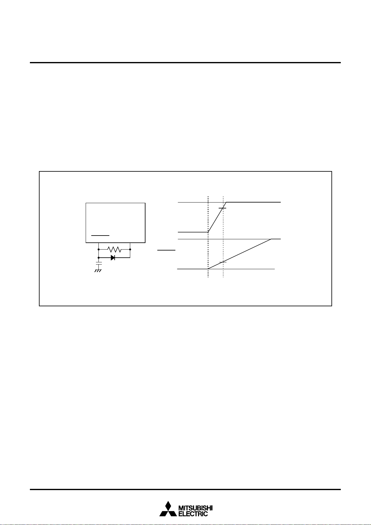
When the supply voltage is in the range where operation is guaranteed, a reset is effected by holding the
reset pin level “L” (0.2VCC max.) for at least 20 cycles. When the reset pin level is then returned to the “H”
level while main clock is stable, the reset status is cancelled and program execution resumes from the
address in the reset vector table.
Figure 2.3.1 shows the example reset circuit. Figure 2.3.2 shows the reset sequence.
RESET
5V
V
CC
0V
V
CC
5V
RESET
0V
4.5V
0.9V
Example when f(XIN) = 10 MHz and VCC = 5V.
Figure 2.3.1 Example reset circuit
2.3.1 Software Reset
Writing “1” to bit 3 of the processor mode register 0 (address 000416) applies a (software) reset to the
microcomputer. A software reset has almost the same effect as a hardware reset. The contents of internal
RAM are preserved.
18
Rev. 1.0
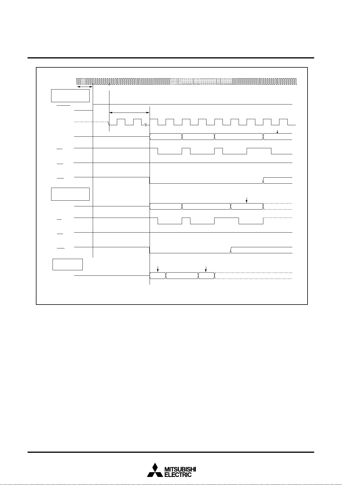
X
IN
Microprocessor
mode BYTE = “H”
MITSUBISHI MICROCOMPUTERS
M306V2ME-XXXFP
M306V2EEFP
SINGLE-CHIP 16-BIT CMOS MICROCOMPUTER with CLOSED CAPTION DECODER
and ON-SCREEN DISPLAY CONTROLLER
More than 20 cycles are needed
RESET
BCLK
Address
RD
WR
CS0
Microprocessor
mode BYTE = “L”
Address
RD
WR
CS0
Single chip
mode
Address
BCLK 24cycles
FFFFC
FFFFC
FFFFC
16
16
16
FFFFE
FFFFD
16
FFFFE
16
Content of reset vector
16
Content of reset vector
FFFFE
16
Content of reset vector
Figure 2.3.2 Reset sequence
Rev. 1.0
19
MITSUBISHI MICROCOMPUTERS
M306V2ME-XXXFP
M306V2EEFP
SINGLE-CHIP 16-BIT CMOS MICROCOMPUTER with CLOSED CAPTION DECODER
and ON-SCREEN DISPLAY CONTROLLER
____________
2.3.2 Pin Status When RESET Pin Level is “L”
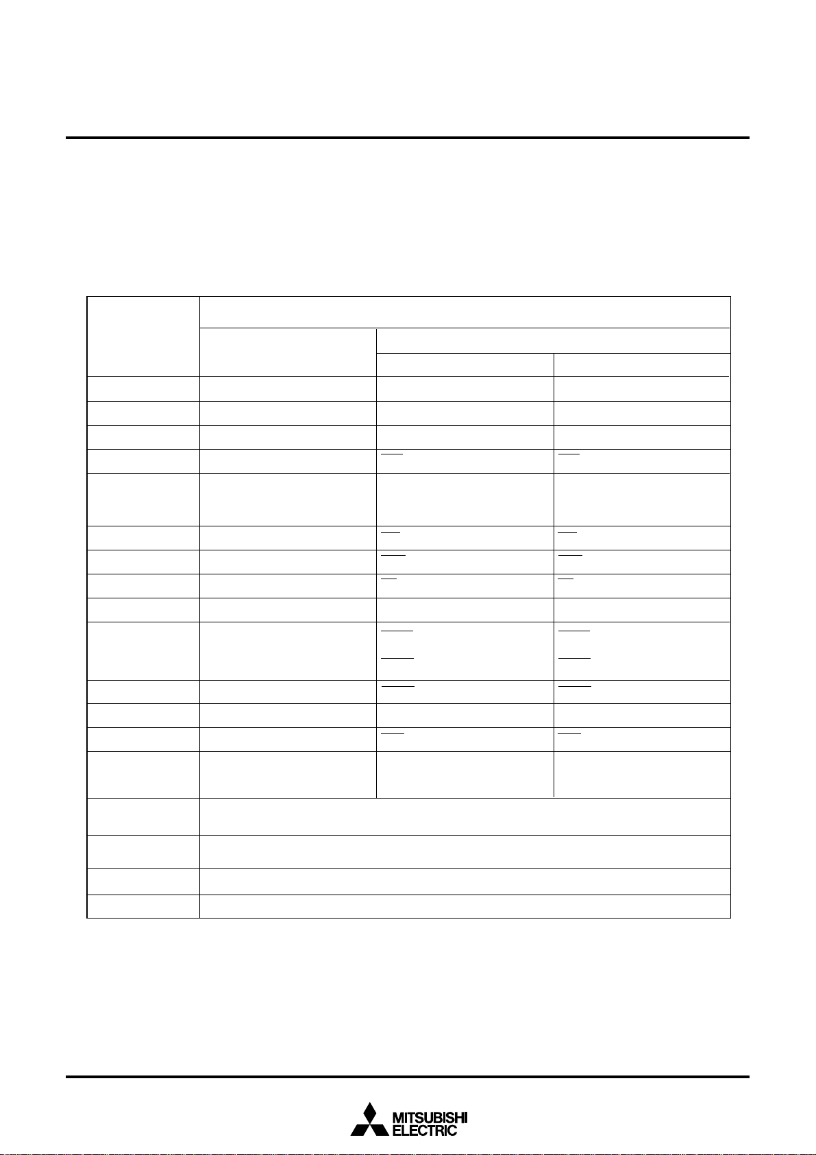
Table 2.3.1 shows the statuses of the other pins while the RESET pin level is “L”. Figures 2.3.3 and 2.3.4
show the internal status of the microcomputer immediately after the reset is cancelled.
____________
Table 2.3.1 Pin status when RESET pin level is “L”
____________
Pin name
P0
P1
P2, P3, P4
P4
4
P45 to P4
P5
0
P5
1
P5
2
P5
3
P5
4
0
7
to P4
Input port (floating)
Input port (floating)
Input port (floating)
3
Input port (floating)
Input port (floating)
Input port (floating)
Input port (floating)
Input port (floating)
Input port (floating)
Input port (floating)
CNVSS = V
SS
Data input (floating)
Data input (floating)
Address output (undefined)
CS0 output (“H” level is output)
Input port (floating)
(pull-up resistor is on)
WR output (“H” level is output)
BHE output (undefined)
RD output (“H” level is output)
BCLK output
HLDA output (The output value
depends on the input to the
HOLD pin)
Status
BYTE = V
SS
CNVSS = V
CC
BYTE = V
Data input (floating)
Input port (floating)
Address output (undefined)
CS0 output (“H” level is output)
Input port (floating)
(pull-up resistor is on)
WR output (“H” level is output)
BHE output (undefined)
RD output (“H” level is output)
BCLK output
HLDA output (The output value
depends on the input to the
HOLD pin)
CC
P5
5
P5
6
P5
7
P60 to P63, P67,
2
P7, P8
P8
, P83,
6
, P87, P9, P10
R, G, B, OUT1,
OUT2
CV
IN
, V
HOLD
,
HLF
OSC1
OSC2
Input port (floating)
Input port (floating)
Input port (floating)
Input port (floating)
Output port
Input/output port
Input port
Output port
HOLD input (floating)
ALE output (“L” level is output)
RDY input (floating)
HOLD input (floating)
ALE output (“L” level is output)
RDY input (floating)
Input port (floating) Input port (floating)
Rev. 1.0
20
MITSUBISHI MICROCOMPUTERS
6
·
r
6
6
6
6
6
6
·
r
r
·
·
·
·
6
r
r
·
·
6
M306V2ME-XXXFP
M306V2EEFP
SINGLE-CHIP 16-BIT CMOS MICROCOMPUTER with CLOSED CAPTION DECODER
and ON-SCREEN DISPLAY CONTROLLER
· ·
( 0 0 0 4
1 6)
· ·
( 0 0 0 51
6)
· ·
1 6)
( 0 0 0 6
· ·
( 0 0 0 7
1 6)
· ·
1 6)
( 0 0 0 8
A d d r e s s m a t c h i n t e r r u p t
e n a b l e r e g i s t e r
P r o t e c t r e g i s t e r(
2
M u l t i - m a s t e r I
i n t e r r u p t c o n t r o l r e g i s t e r
B u s c o l l i s i o n d e t e c t i o n i n t e r r u p t
c o n t r o l r e g i s t e r
D M A 0 i n t e r r u p t c o n t r o l r e g i s t e
C - B U S i n t e r f a c e 1
M u l t i - m a s t e r I
i n t e r r u p t c o n t r o l r e g i s t e r
A - D c o n v e r s i o n i n t e r r u p t
c o n t r o l r e g i s t e r
U A R T 2 t r a n s m i t i n t e r r u p t
c o n t r o l r e g i s t e r
U A R T 2 r e c e i v e i n t e r r u p t
c o n t r o l r e g i s t e r
U A R T 0 t r a n s m i t i n t e r r u p t
c o n t r o l r e g i s t e r
U A R T 0 r e c e i v e i n t e r r u p t
c o n t r o l r e g i s t e r
2
C - B U S i n t e r f a c e 0
D a t a s l i c e r i n t e r r u p t c o n t r o l r e g i s t e r
i n t e r r u p t c o n t r o l r e g i s t e
V
S Y N C
T i m e r A 0 i n t e r r u p t c o n t r o l r e g i s t e r
T i m e r A 1 i n t e r r u p t c o n t r o l r e g i s t e r
T i m e r A 2 i n t e r r u p t c o n t r o l r e g i s t e r
T i m e r A 3 i n t e r r u p t c o n t r o l r e g i s t e r
T i m e r A 4 i n t e r r u p t c o n t r o l r e g i s t e r
· ·
( 0 0 0 9
1 6)
· ·
0 0 0
1 6)
A
· ·
( 0 0 0 F1
6)
· ·
( 0 0 1 0
1 6)
· ·
1 6)
( 0 0 1 1
· ·
1 6)
( 0 0 1 2
· ·
( 0 0 1 4
1 6)
· ·
1 6)
( 0 0 1 5
· ·
1 6)
( 0 0 1 6
· ·
( 0 0 2 C
1 6)
· ·
1 6)
( 0 0 3 C
· ·
1 6)
( 0 0 4 4
· ·
( 0 0 4 81
6)
· ·
( 0 0 4 91
6)
· ·
( 0 0 4 A
1 6)
· ·
( 0 0 4 B1
6)
· ·
1 6)
( 0 0 4 C
· ·
( 0 0 4 D
1 6)
· ·
1 6)
( 0 0 4 E
· ·
( 0 0 4 F
1 6)
· ·
1 6)
( 0 0 5 0
· ·
1 6)
( 0 0 5 1
· ·
( 0 0 5 2
1 6)
· ·
1 6)
( 0 0 5 3
· ·
r
( 0 0 5 4
1 6)
· ·
1 6)
( 0 0 5 5
· ·
( 0 0 5 6
1 6)
· ·
1 6)
( 0 0 5 7
· ·
1 6)
( 0 0 5 8
· ·
( 0 0 5 9
1 6)
·P r o c e s s o r m o d e r e g i s t e r 0 ( N o t e ) 0 01
·P r o c e s s o r m o d e r e g i s t e r 1
4 81
·S y s t e m c l o c k c o n t r o l r e g i s t e r 0
2 01
·S y s t e m c l o c k c o n t r o l r e g i s t e r 1
0 11
·C h i p s e l e c t c o n t r o l r e g i s t e r
·
·W a t c h d o g t i m e r c o n t r o l r e g i s t e
00?0 ????
·A d d r e s s m a t c h i n t e r r u p t r e g i s t e r 0
0 01
·
0 01
· 0
·A d d r e s s m a t c h i n t e r r u p t r e g i s t e r 1
0 01
·
0 01
· 0
·D M A 0 c o n t r o l r e g i s t e r 00000?00
·D M A 1 c o n t r o l r e g i s t e r 00000?00
·O S D 1 i n t e r r u p t c o n t r o l r e g i s t e r ?000
·O S D 2 i n t e r r u p t c o n t r o l r e g i s t e r
·
·D M A 1 i n t e r r u p t c o n t r o l r e g i s t e
· ? 0 0 0
· ? 0 0 0
·
·
·
·
·
·
·
·
·
·
·
l e v e l i s a p p l i e d t o t h e C N
p i n , i t i s 0
a t a r e s e t
T h e c o n t e n t o f o t h e r r e g i s t e r s a n d R A M i s u n d e f i n e d w h e n t h e m i c r o c o m p u t e r i s r e s e t . T h e i n i t i a l v a l u e s
m u s t t h e r e f o r e b e s e t .
N o t e : W h e n t h e VC
00 0
000
0 0 0
0 0 0
?000
?00000
0 0 0?
? 0 0 0
? 0 0 0
? 0 0 0
? 0 0 0
? 0 0 0
? 0 0 0
? 0 0 0
? 0 0 0
? 0 0 0
? 0 0 0
? 0 0 0
? 0 0 0
? 0 0 0
T i m e r B 0 i n t e r r u p t c o n t r o l r e g i s t e r
0
000
T i m e r B 1 i n t e r r u p t c o n t r o l r e g i s t e r
T i m e r B 2 i n t e r r u p t c o n t r o l r e g i s t e r
I N T 0 i n t e r r u p t c o n t r o l r e g i s t e r
I N T 1 i n t e r r u p t c o n t r o l r e g i s t e r
00
S P R I T E O S D c o n t r o l r e g i s t e r
O S D c o n t r o l r e g i s t e r 1
O S D c o n t r o l r e g i s t e r 2
H o r i z o n t a l p o s i t i o n r e g i s t e r
C l o c k c o n t r o l r e g i s t e r
I / O p o l a r i t y c o n t r o l r e g i s t e r
O S D c o n t r o l r e g i s t e r 3
R a s t e r c o l o r r e g i s t e r
O S D r e s e r v e d r e g i s t e r 1(
O S D c o n t r o l r e g i s t e r 4
D a t a s l i c e r c o n t r o l r e g i s t e r 1
D a t a s l i c e r c o n t r o l r e g i s t e r 2
C a p t i o n p o s i t i o n r e g i s t e r
D a t a s l i c e r r e s e r v e d r e g i s t e r 2(
D a t a s l i c e r r e s e r v e d r e g i s t e r 1(
C l o c k r u n - i n d e t e c t r e g i s t e r
D a t a c l o c k p o s i t i o n r e g i s t e r
L e f t b o r d e r c o n t r o l r e g i s t e r
R i g h t b o r d e r c o n t r o l r e g i s t e r
S P R I T E h o r i z o n t a l p o s i t i o n r e g i s t e r
( h i g h - o r d e r )
O S D r e s e r v e d r e g i s t e r 4
O S D r e s e r v e d r e g i s t e r 3
O S D r e s e r v e d r e g i s t e r 2
P e r i p h e r a l m o d e r e g i s t e
c o u n t e r r e g i s t e
H
S Y N C
X : N o t h i n g i s m a p p e d t o t h i s b i t
? : U n d e f i n e d
C
VS
S
31
6
· ·
( 0 0 5 A
· ·
( 0 0 5 B1
· ·
( 0 0 5 C
· ·
( 0 0 5 D
· ·
( 0 0 5 E
· ·
( 0 2 0 1
· ·
( 0 2 0 21
· ·
( 0 2 0 31
· ·
( 0 2 0 41
· ·
( 0 2 0 5
· ·
( 0 2 0 61
· ·
( 0 2 0 71
· ·
( 0 2 0 8
· ·
( 0 2 0 9
0 2 5
· ·
· ·
( 0 2 5 F
· ·
( 0 2 6 01
· ·
( 0 2 6 11
· ·
( 0 2 6 6
· ·
0 2 6
0 2 6
· ·
· ·
( 0 2 6 9
· ·
( 0 2 6 A1
· ·
( 0 2 7 0
· ·
( 0 2 7 11
· ·
( 0 2 7 2
· ·
( 0 2 7 3
· ·
( 0 2 7 9
· ·
( 0 2 7 A
· ·
( 0 2 7 B1
· ·
( 0 2 7 C
· ·
( 0 2 7 D1
· ·
( 0 2 7 E1
1 6)
6)
1 6)
1 6)
1 6)
1 6)
6)
6)
6)
1 6)
6)
6)
1 6)
1 6)
D1
6)
1 6)
6)
6)
1 6)
1 6)
7
81
6)
1 6)
6)
1 6)
6)
1 6)
1 6)
1 6)
1 6)
6)
1 6)
6)
6)
· ? 0 0 0
·
· 00000
·
· 0 01
·
· 0 01
·
·
·
·
· 0 01
·
· 0 01
· 000
?
0000
·
· 0 01
· 0 01
· 0 01
·
·
·
·
·
·
·
·
00000
·
? 0 0 0
? 0 0 0
? 00000
? 00000
0 01
6
6
0 01
6
6
00000010
0 01
6
0 01
6
0 01
6
6
00
6
????
?
000
6
6
6
00 010
0 11
6
000
0 01
000
000
00 00000
0 01
6
0 01
6
0
00 00
.
Figure 2.3.3 Device’s internal status after a reset is cleared (1)
Rev. 1.0
21
MITSUBISHI MICROCOMPUTERS
M306V2ME-XXXFP
M306V2EEFP
SINGLE-CHIP 16-BIT CMOS MICROCOMPUTER with CLOSED CAPTION DECODER
and ON-SCREEN DISPLAY CONTROLLER
2
I
C0 address register
2
I
C0 status register
I2C0 control register
I2C0 clock control register
2
C0 port selection register
I
2
C1 address register
I
2
I
C1 status register
I2C1 control register
I2C1 clock control register
2
C1 port selection register
I
Reserved register 1
Reserved register 0
Interrupt request cause select register
Reserved register 3
Reserved register 4
Reserved register 5
UART2 special mode register
UART2 transmit/receive mode register
UART2 transmit/receive control register 0
UART2 transmit/receive control register 1
Count start flag
Reserved register 2
(02E1
16
)···
(02E216)···
16
(02E3
(02E4
16
16
(02E5
(02E9
16
(02EA
16
16
(02EB
(02EC
16
16
(02ED
(0340
16
16
(0348
16
(035F
(0362
16
16
(0366
16
(0376
000
)··· 00
)··· 00
)···
?00
)···
)···
000
)··· 00
)··· 00
)···
?00
000
)···
)··· 00
)··· 00
)··· 40
)··· 40
)··· 00
(037716)··· 00
(037816)··· 00
(037C
16
)···
(037D
16
)···
16
)··· 00
(0380
(0381
(0382
(0383
(0384
(0396
(0397
(0398
(0399
(039A
(039B
(039C
(039D
(03A0
(03A4
(03A5
(03A8
0
16
)···Clock prescaler reset flag
16
)···One-shot start flag
0000 000
16
)···Trigger select register
16
)···Up-down flag
16
)···Timer A0 mode register
16
)···Timer A1 mode register
16
)···Timer A2 mode register
16
)···Timer A3 mode register
16
)···Timer A4 mode register
16
)···Timer B0 mode register
0
0? 0000
16
)···Timer B1 mode register
00? 0000
16
)···Timer B2 mode register
00? 0000
16
)···UART0 transmit/receive mode register
16
)···UART0 transmit/receive control register 0
16
)···UART0 transmit/receive control register 1
16
)··· 00
The content of other registers and RAM is undefined when the microcomputer is reset. The initial values
must therefore be set.
Note: When the V
00
16
000
1?
16
16
000
?0
00
16
000
1?
16
16
000
?0
???
??
16
16
16
16
16
16
16
08
16
02
16
16
00
16
00
16
00
16
00
16
00
16
00
16
00
16
00
16
08
16
02
16
16
CC
level is applied to the CNVSS pin, it is 0216 at a reset.
A-D control register 0
A-D control register 1
D-A control register
Port P0 direction register
Port P1 direction register
Port P2 direction register
Port P3 direction register
Port P4 direction register
Port P5 direction register
Port P6 direction register
Port P7 direction register
Port P8 direction register
Port P9 direction register
Port P10 direction register
Pull-up control register 0
Pull-up control register 1(Note)
Pull-up control register 2
Port control register
Data registers (R0/R1/R2/R3)
Address registers (A0/A1)
Frame base register (FB)
Interrupt table register (INTB)
User stack pointer (USP)
Interrupt stack pointer (ISP)
Static base register (SB)
Flag register (FLG)
x : Nothing is mapped to this bit
? : Undefined
(03B0
16
)···UART transmit/receive control register 2
(03B816)···DMA0 request cause select register
16
)···DMA1 request cause select register
(03BA
(03D416)···A-D control register 2 0???
(03D616)···
16
)···
(03D7
(03DC
16
)··· 00
(03E2
16
)···
16
)···
(03E3
16
)···
(03E6
16
)···
(03E7
16
)···
(03EA
16
)···
(03EB
16
)···
(03EE
16
)···
(03EF
16
)···
(03F2
16
)···
(03F3
16
)···
(03F6
16
)···
(03FC
16
)···
(03FD
16
)···
(03FE
16
)··· 00
(03FF
00
00
0000
000 0???0
00
00
00
00
00
00
00
00
00
00 00000
00
00
00
00
00
0000
0000
0000
00000
0000
0000
0000
0000
0000000
16
16
16
16
16
16
16
16
16
16
16
16
16
16
16
16
16
16
16
16
16
16
16
16
16
16
Figure 2.3.4 Device’s internal status after a reset is cleared (2)
22
Rev. 1.0

MITSUBISHI MICROCOMPUTERS
M306V2ME-XXXFP
M306V2EEFP
SINGLE-CHIP 16-BIT CMOS MICROCOMPUTER with CLOSED CAPTION DECODER
and ON-SCREEN DISPLAY CONTROLLER
2.4 Processor Mode
2.4.1 Types of Processor Mode
One of three processor modes can be selected: single-chip mode, memory expansion mode, and microprocessor mode. The functions of some pins, the memory map, and the access space differ according to
the selected processor mode.
(1) Single-chip mode
In single-chip mode, only internal memory space (SFR, OSD RAM, internal RAM, and internal ROM)
can be accessed. Ports P0 to P10 can be used as programmable I/O ports or as I/O ports for the
internal peripheral functions.
(2) Memory expansion mode
In memory expansion mode, external memory can be accessed in addition to the internal memory
space (SFR, OSD RAM, internal RAM, and internal ROM).
In this mode, some of the pins function as the address bus, the data bus, and as control signals. The
number of pins assigned to these functions depends on the bus and register settings. (See “2.4.3 Bus
Settings” for details.)
(3) Microprocessor mode
In microprocessor mode, the SFR, OSD RAM, internal RAM, and external memory space can be
accessed. The internal ROM area cannot be accessed.
In this mode, some of the pins function as the address bus, the data bus, and as control signals. The
number of pins assigned to these functions depends on the bus and register settings. (See “2.4.3 Bus
Settings” for details.)
2.4.2 Setting Processor Modes
The processor mode is set using the CNVSS pin and the processor mode bits (bits 1 and 0 at address
000416). Do not set the processor mode bits to “102”.
Regardless of the level of the CNVSS pin, changing the processor mode bits selects the mode. Therefore,
never change the processor mode bits when changing the contents of other bits. Also do not attempt to
shift to or from the microprocessor mode within the program stored in the internal ROM area.
(1) Applying VSS to CNVSS pin
The microcomputer begins operation in single-chip mode after being reset. Memory expansion mode
is selected by writing “012” to the processor mode is selected bits.
(2) Applying VCC to CNVSS pin
The microcomputer starts to operate in microprocessor mode after being reset.
Figures 2.4.1 and 2.4.2 show the processor mode register 0 and 1.
Figure 2.4.3 shows the memory maps applicable for each of the modes.
Rev. 1.0
23
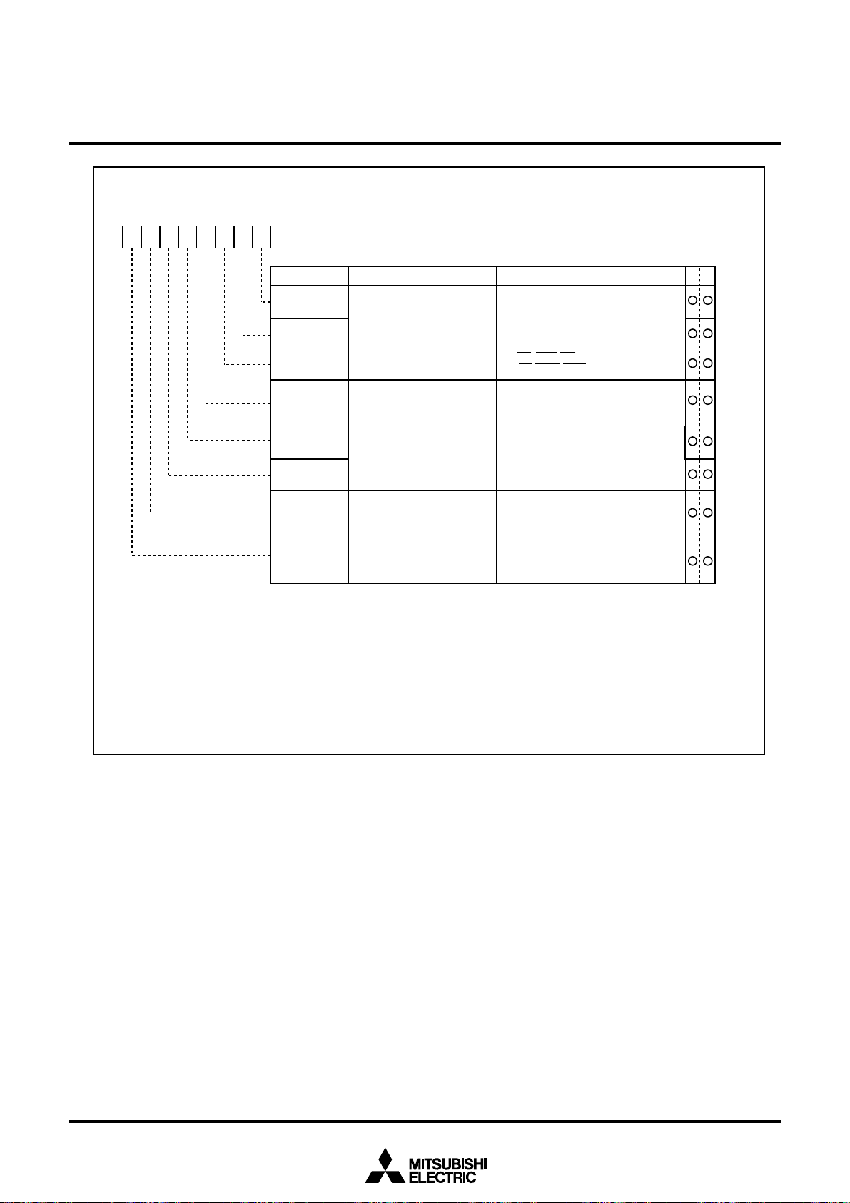
MITSUBISHI MICROCOMPUTERS
M306V2ME-XXXFP
M306V2EEFP
SINGLE-CHIP 16-BIT CMOS MICROCOMPUTER with CLOSED CAPTION DECODER
and ON-SCREEN DISPLAY CONTROLLER
P r o c e s s o r m o d e r e g i s t e r 0 ( N o t e 1 )
d d r e s
h e n r e s e
0 0
b 7b 6b 5b 4b 3b 2b 1b 0
S y m b o lA
P M 00
P M 0 0
P M 0 1
P M 0 2
P M 0 3
P M 0 4
P M 0 5
P M 0 6
P M 0 7
N o t e s 1 : S e t b i t 1 o f t h e p r o t e c t r e g i s t e r ( a d d r e s s 0 0 0 A
v a l u e s t o t h i s r e g i s t e r .
2 : I f t h e V
r e s e t i s 0 3
3 : V a l i d i n m i c r o p r o c e s s o r a n d m e m o r y e x p a n s i o n m o d e s .
4 : I f t h e e n t i r e s p a c e i s o f m u l t i p l e x e d b u s i n m e m o r y e x p a n s i o n m o d e , c h o o s e a n 8 -
b i t w i d t h .
T h e p r o c e s s o r o p e r a t e s u s i n g t h e s e p a r a t e b u s a f t e r r e s e t i s r e v o k e d , s o t h e
e n t i r e s p a c e m u l t i p l e x e d b u s c a n n o t b e c h o s e n i n m i c r o p r o c e s s o r m o d e .
T h e h i g h e r - o r d e r a d d r e s s b e c o m e s a p o r t i f t h e e n t i r e s p a c e m u l t i p l e x e d b u s i s
c h o s e n , s o o n l y 2 5 6 b y t e s c a n b e u s e d i n e a c h c h i p s e l e c t .
sW
4
1 6
0 0
1 6
B i t n a m eF
P r o c e s s o r m o d e b i t
R / W m o d e s e l e c t b i t
S o f t w a r e r e s e t b i t
M u l t i p l e x e d b u s s p a c e
s e l e c t b i t
P o r t P 40 t o P 43 f u n c t i o n
s e l e c t b i t ( N o t e 3 )
B C L K o u t p u t d i s a b l e b i t
T h e d e v i c e i s r e s e t w h e n t h i s b i t i s s e t
t o “ 1 ” . T h e v a l u e o f t h i s b i t i s “ 0 ” w h e n
r e a d .
b 5 b 4
0 : A d d r e s s o u t p u t
1 : P o r t f u n c t i o n
( A d d r e s s i s n o t o u t p u t )
0 : B C L K i s o u t p u t
t
( N o t e 2 )
u n c t i o
b 1 b 0
0 0 : S i n g l e - c h i p m o d e
0 1 : M e m o r y e x p a n s i o n m o d e
1 0 : I n h i b i t e d
1 1 : M i c r o p r o c e s s o r m o d e
0 : R D , B H E , W R
1 : R D , W R H , W R L
0 0 : M u l t i p l e x e d b u s i s n o t u s e d
0 1 : A l l o c a t e d t o C S 2 s p a c e
1 0 : A l l o c a t e d t o C S 1 s p a c e
1 1 : A l l o c a t e d t o e n t i r e s p a c e ( N o t e 4 )
1 : B C L K i s n o t o u t p u t
( P i n i s l e f t f l o a t i n g )
1 6
) t o “ 1 ” w h e n w r i t i n g n e w
C C
v o l t a g e i s a p p l i e d t o t h e C N V
1 6
. ( P M 0 0 a n d P M 0 1 b o t h a r e s e t t o “ 1 ” . )
S S
, t h e v a l u e o f t h i s r e g i s t e r w h e n
nB i t s y m b o l
WR
Figure 2.4.1 Processor mode register 0
24
Rev. 1.0
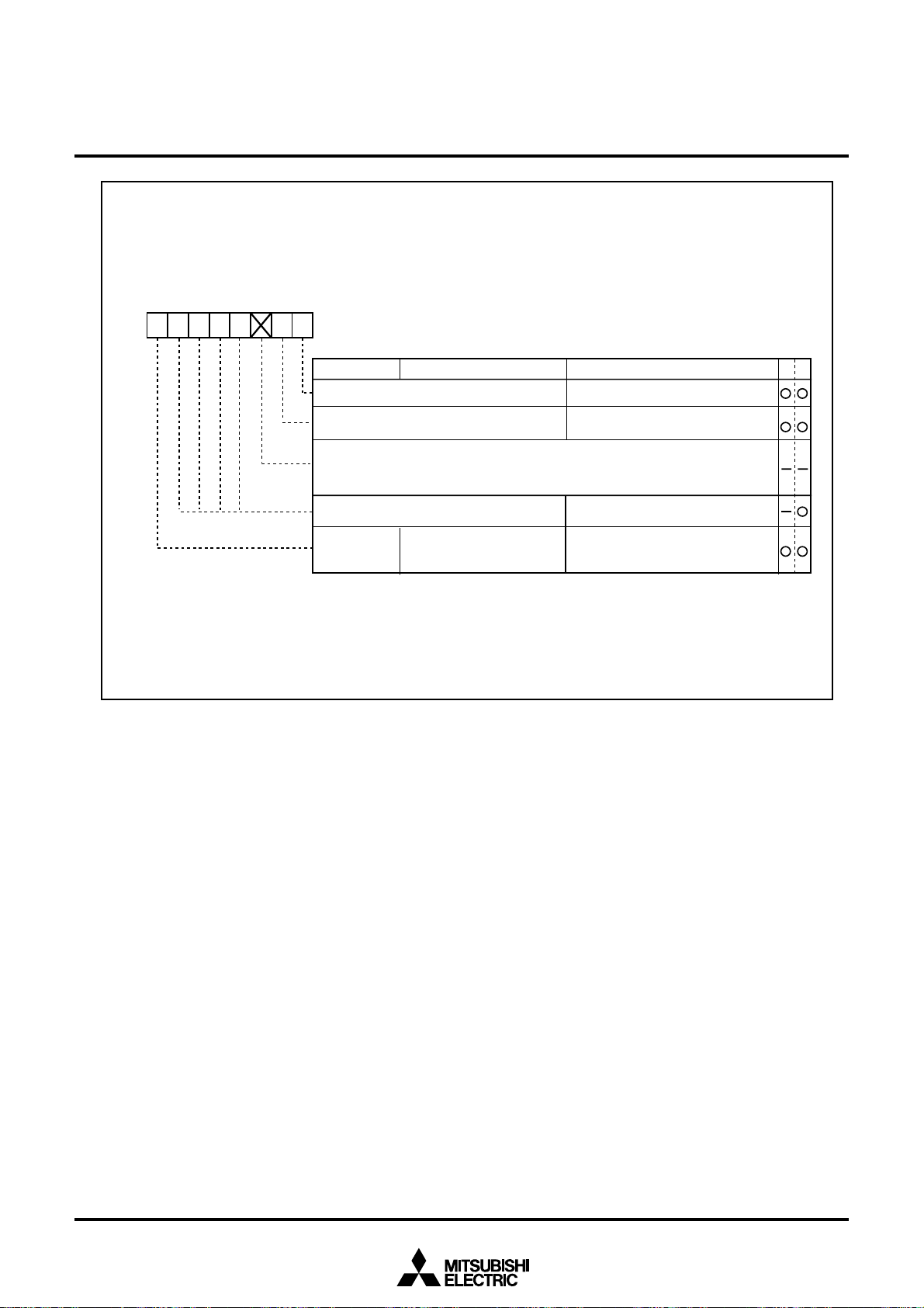
SINGLE-CHIP 16-BIT CMOS MICROCOMPUTER with CLOSED CAPTION DECODER
P r o c e s s o r m o d e r e g i s t e r 1 ( N o t e 1 )
d d r e s
h e n r e s e
0 0
b 7b 6b 5b 4b 3b 2b 1b 0
0
000
1
0
0 0 0 0 X 0
S y m b o lA
P M 10
and ON-SCREEN DISPLAY CONTROLLER
sW
5
1 6 0
MITSUBISHI MICROCOMPUTERS
M306V2ME-XXXFP
M306V2EEFP
t
02
R e s e r v e d b i t
R e s e r v e d b i t ( N o t e 2 )
N o t h i n g i s a s s i g n e d .
I n a n a t t e m p t t o w r i t e t o t h i s b i t , w r i t e “ 0 . ” T h e v a l u e , i f r e a d , t u r n s o u t t o b e
i n d e t e r m i n a t e .
R e s e r v e d b i t s
P M 1 7
t o “ 1 ” w h e n w r i t i n g n e w
N o t e s 1 : S e t b i t 1 o f t h e p r o t e c t r e g i s t e r ( a d d r e s s 0 0 0 A
v a l u e s t o t h i s r e g i s t e r .
2: A s t h i s b i t b e c o m e s “ 0 ” a t r e s e t , m u s t a l w a y s b e s e t t o “ 1 ” a f t e r r e s e t
r e l e a s e .
Figure 2.4.2 Processor mode register 1
W a i t b i t
1 6)
u n c t i o
nB i t s y m b o l
B i t n a m eF
M u s t a l w a y s b e s e t t o “ 0 ”
M u s t a l w a y s b e s e t t o “ 1 ”
M u s t a l w a y s b e s e t t o “ 0 ”
0 : N o w a i t s t a t e
1 : W a i t s t a t e i n s e r t e d
WR
Rev. 1.0
25
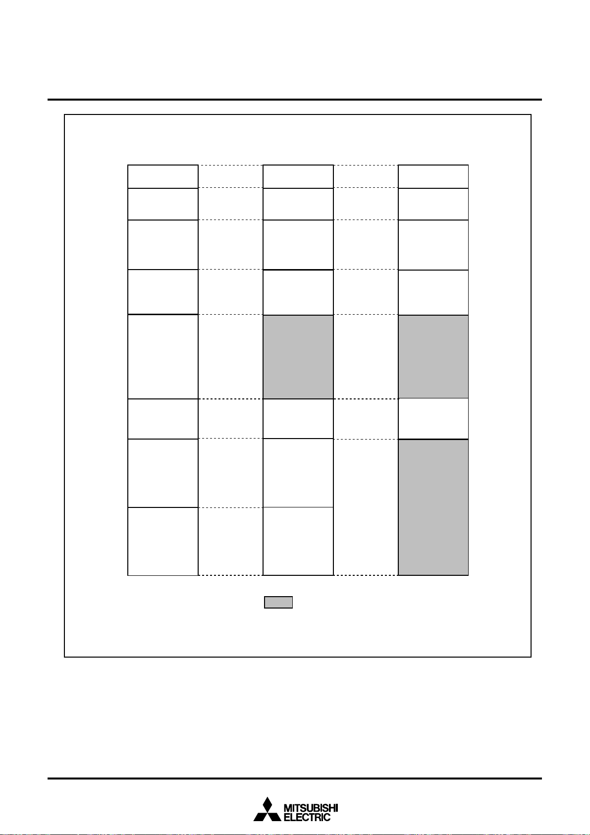
MITSUBISHI MICROCOMPUTERS
M306V2ME-XXXFP
M306V2EEFP
SINGLE-CHIP 16-BIT CMOS MICROCOMPUTER with CLOSED CAPTION DECODER
and ON-SCREEN DISPLAY CONTROLLER
00000
003FF
00400
013FF
01400
02BFF
02C00
03FFF
04000
8FFFF
90000
AFFFF
B0000
Single-chip mode
16
SFR area
16
16
OSD RAM
16
16
Internal
reserved area
16
16
Internal
RAM area
16
16
Not used
16
16
OSD ROM
16
16
Memory expansion mode Microprocessor mode
SFR area
OSD RAM
Internal
reserved area
Internal RAM
area
External area
OSD ROM OSD ROM
SFR area
OSD RAM
Internal
reserved area
Internal RAM
area
External area
Internal
reserved area
Internal
ROM area
CFFFF
D0000
FFFFF
Internal
reserved area
16
16
Internal
ROM area
16
External area : Accessing this area allows you to
Figure 2.4.3 Memory maps in each processor mode
External area
access a device connected external
to the microcomputer.
26
Rev. 1.0
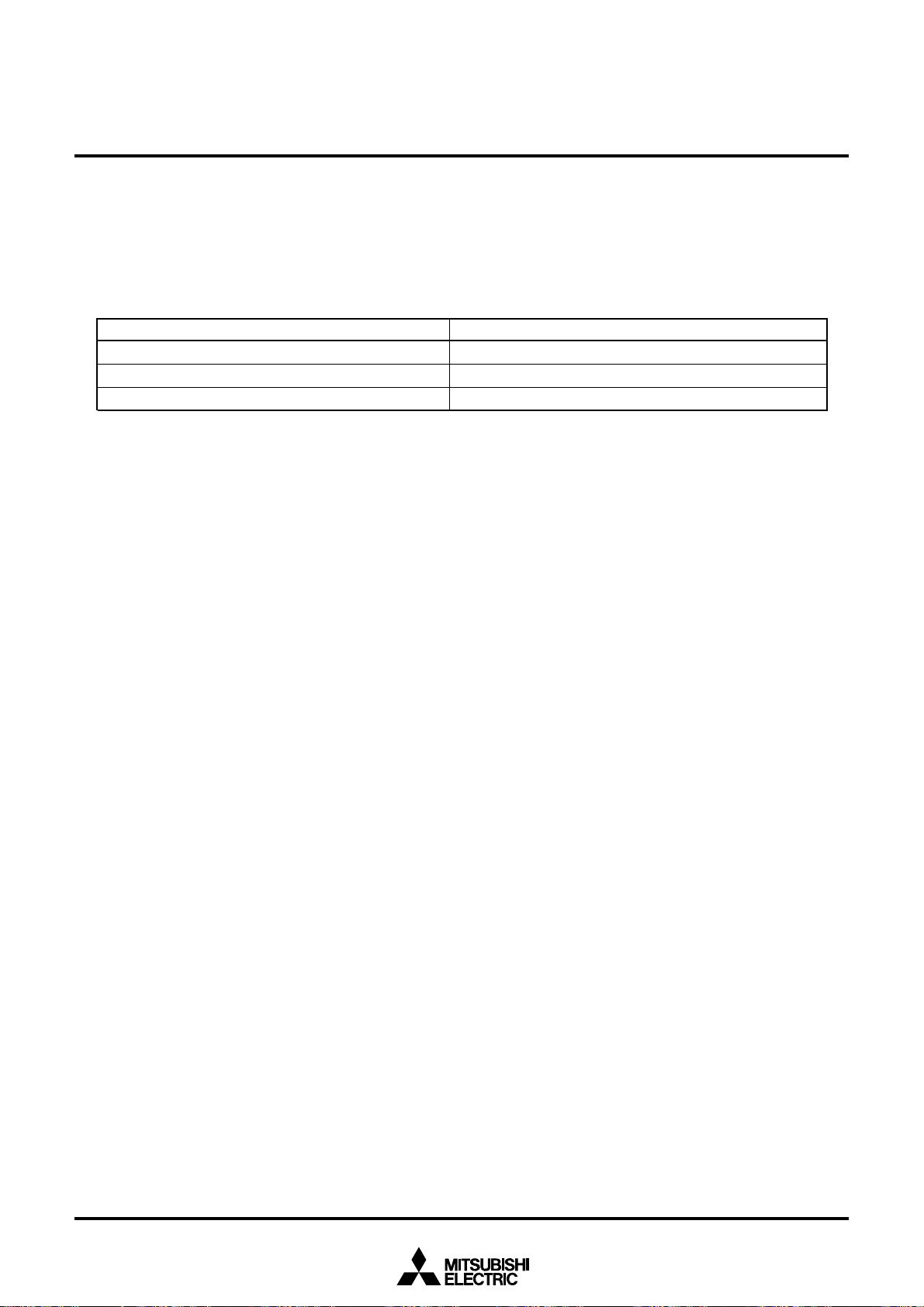
MITSUBISHI MICROCOMPUTERS
M306V2ME-XXXFP
M306V2EEFP
SINGLE-CHIP 16-BIT CMOS MICROCOMPUTER with CLOSED CAPTION DECODER
and ON-SCREEN DISPLAY CONTROLLER
2.4.3 Bus Settings
The BYTE pin and bits 4 to 6 of the processor mode register 0 (address 000416) are used to change the
bus settings.
Table 2.4.1 shows the factors used to change the bus settings.
Table 2.4.1 Factors for switching bus settings
Bus setting Switching factor
Switching external address bus width Bit 6 of processor mode register 0
Switching external data bus width BYTE pin
Switching between separate and multiplex bus Bits 4 and 5 of processor mode register 0
(1) Selecting external address bus width
The address bus width for external output in the 1M bytes of address space can be set to 16 bits (64K
bytes address space) or 20 bits (1M bytes address space). When bit 6 of the processor mode register
0 is set to “1”, the external address bus width is set to 16 bits, and P2 and P3 become part of the
address bus. P40 to P43 can be used as programmable I/O ports. When bit 6 of processor mode
register 0 is set to “0”, the external address bus width is set to 20 bits, and P2, P3, and P40 to P43
become part of the address bus.
(2) Selecting external data bus width
The external data bus width can be set to 8 or 16 bits. (Note, however, that only the separate bus can
be set.) When the BYTE pin is “L”, the bus width is set to 16 bits; when “H”, it is set to 8 bits. (The
internal bus width is permanently set to 16 bits.)
While operating, fix the BYTE pin either to “H” or to “L.”
(3) Selecting separate/multiplex bus
The bus format can be set to multiplex or separate bus using bits 4 and 5 of the processor mode
register 0.
• Separate bus
In this mode, the data and address are input and output separately. The data bus can be set using the
BYTE pin to be 8 or 16 bits. When the BYTE pin is “H”, the data bus is set to 8 bits and P0 functions as
the data bus and P1 as a programmable I/O port. When the BYTE pin is “L”, the data bus is set to 16
bits and P0 and P1 are both used for the data bus.
When the separate bus is used for access, a software wait can be selected.
• Multiplex bus
In this mode, data and address I/O are time multiplexed. With an 8-bit data bus selected (BYTE pin =
“H”), the 8 bits from D0 to D7 are multiplexed with A0 to A7.
With a 16-bit data bus selected (BYTE pin = “L”), the 8 bits from D0 to D7 are multiplexed with A1 to A8.
D8 to D15 are not multiplexed. In this case, the external devices connected to the multiplexed bus are
mapped to the microcomputer’s even addresses (every 2nd address). To access these external devices, access the even addresses as bytes.
The ALE signal latches the address. It is output from P56.
Before using the multiplex bus for access, be sure to insert a software wait.
Rev. 1.0
27
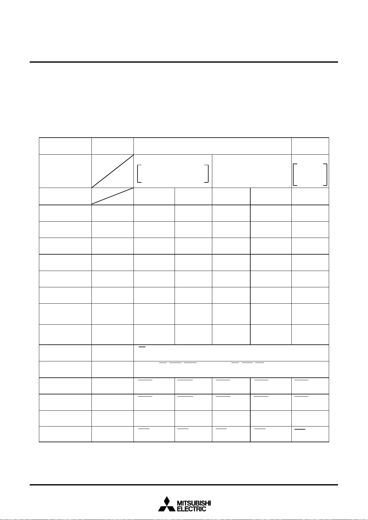
MITSUBISHI MICROCOMPUTERS
M306V2ME-XXXFP
M306V2EEFP
SINGLE-CHIP 16-BIT CMOS MICROCOMPUTER with CLOSED CAPTION DECODER
and ON-SCREEN DISPLAY CONTROLLER
In memory expansion mode, select a 8-bit multiplex bus.
The processor operates using the separate bus after reset is revoked, so the entire space multiplexed
bus cannot be chosen in microprocessor mode.
The higher-order address becomes a port if the entire space multiplexed bus is chosen, so only 256
bytes can be used in each chip select.
Table 2.4.2 Pin functions for each processor mode
P r o c e s s o r m o d e
M u l t i p l e x e d b u s
s p a c e s e l e c t b i t
D a t a b u s w i d t h
B Y T E p i n l e v e l
a t a b u
a t a b u
a t a b u
a t a b u
/ O p o r
P 00 t o P 0
/ O p o r
a t a b u
/ O p o r
a t a b u
/ O p o r
P 1
P 2
d d r e s s b u
P 2
d d r e s s b u
P 3
d d r e s s b u
P 3
/ O p o r
/ O p o r
O p o r
/ O p o r
/ O p o r
P 4
P o r t P 40 t o P 4
f u n c t i o n s e l e c t b i t = 1
d d r e s s b u
P 4
P o r t P 40 t o P 4
f u n c t i o n s e l e c t b i t = 0
P 4
P 5
L D
L D
L D
L D
L D
P 5
0
t o P 1
0
1
t o P 2
0
1
t o P 3
0
t o P 4
0
t o P 4
4
t o P 4
0
t o P 5
4
7
7
7
7
3
3
3
3
7
3
S i n g l e - c h i p
m o d e
M e m o r y e x p a n s i o n m o d e / m i c r o p r o c e s s o r m o d e s
E i t h e r C S 1 o r C S 2 i s f o r
m u l t i p l e x e d b u s a n d o t h e r s
a r e f o r s e p a r a t e b u s
8 b i t s
= “ H ”
I / O p o r tD
I / O p o r tI
I / O p o r t
I / O p o r t
A d d r e s s b u s
/ d a t a b u s
A d d r e s s b u sA
I / O p o r tA
/ d a t a b u s
I / O p o r tA
I / O p o r tI
I / O p o r tA
I / O p o r t
I / O p o r t
I / O p o r tH
C S ( c h i p s e l e c t ) o r p r o g r a m m a b l e I / O p o r t
O u t p u t s R D , W R L , W R H , a n d B C L K o r R D , B H E , W R , a n d B C L K
AH
e x p a n s i o n m o d e
“ 0 1 ” , “ 1 0 ”“
0 0
”“
( s e p a r a t e b u s )
1 6 b i t s
= “ L ”
sD
tD
sD
sI
8 b i t s
= “ H ”
sD
tD
1 6 b i t s
= “ L ”
sI
sI
A d d r e s s b u sA d d r e s s b u sA d d r e s s b u sA d d r e s s b u s
( N o t e 3 )
s
A d d r e s s b u sA d d r e s s b u sA d d r e s s b u s
/ d a t a b u s
( N o t e 3 )
A d d r e s s b u sA d d r e s s b u sA8/ D
s
( N o t e 3 )
/ d a t a b u s
A d d r e s s b u s
( N o t e 3 )
sA d d r e s s b u sA d d r e s s b u sA d d r e s s b u sI / O p o r t
tI
t/
tI
tI
sA d d r e s s b u sA d d r e s s b u sA d d r e s s b u sI / O p o r t
( F o r d e t a i l s , r e f e r t o “ 2 . 4 . 4 B u s c o n t r o l ” )
( F o r d e t a i l s , r e f e r t o “ 2 . 4 . 4 B u s c o n t r o l ” )
AH
AH
AH
M e m o r y
1 1 ” ( N o t e 1
M u l t i p l e x e d
b u s f o r t h e
e n t i r e
s p a c e
8 b i t s
= “ H ”
t
t
/ d a t a b u s
/ d a t a b u s
7
t
A
)
O L
O L
O L
O L
O L
P 5
D
D
D
D
D
L
L
L
L
L
P 5
P 5
5
6
7
I / O p o r tH
I / O p o r tA
I / O p o r tR
DH
EA
YR
N o t e s 1 : I n m e m o r y e x p a n s i o n m o d e , s e l e c t a 8 - b i t m u l t i p l e x b u s .
T h e p r o c e s s o r o p e r a t e s u s i n g t h e s e p a r a t e b u s a f t e r r e s e t i s r e v o k e d , s o t h e e n t i r e s p a c e m u l t i p l e x e d b u s c a n n o t b e
c h o s e n i n m i c r o p r o c e s s o r m o d e .
T h e h i g h e r - o r d e r a d d r e s s b e c o m e s a p o r t i f t h e e n t i r e s p a c e m u l t i p l e x e d b u s i s c h o s e n , s o o n l y 2 5 6 b y t e s c a n b e
u s e d i n e a c h c h i p s e l e c t .
2 : A d d r e s s b u s w h e n i n s e p a r a t e b u s m o d e .
28
DH
EA
YR
DH
EA
YR
DH
EA
YR
D
E
Y
Rev. 1.0
MITSUBISHI MICROCOMPUTERS
M306V2ME-XXXFP
M306V2EEFP
SINGLE-CHIP 16-BIT CMOS MICROCOMPUTER with CLOSED CAPTION DECODER
and ON-SCREEN DISPLAY CONTROLLER
2.4.4 Bus Control
The following explains the signals required for accessing external devices and software waits. The signals required for accessing the external devices are valid when the processor mode is set to memory
expansion mode and microprocessor mode. The software waits are valid in all processor modes.
(1) Address bus/data bus
The address bus consists of the 20 pins A0 to A19 for accessing the 1M bytes of address space.
The data bus consists of the pins for data I/O. When the BYTE pin is “H”, the 8 ports D0 to D7 function
as the data bus. When BYTE is “L”, the 16 ports D0 to D15 function as the data bus.
When a change is made from single-chip mode to memory expansion mode, the value of the address
bus is undefined until external memory is accessed.
(2) Chip select signal
The chip select signal is output using the same pins as P44 to P47. Bits 0 to 3 of the chip select control
register (address 000816) set each pin to function as a port or to output the chip select signal. The chip
select control register is valid in memory expansion mode and microprocessor mode. In single-chip
mode, P44 to P47 function as programmable I/O ports regardless of the value in the chip select control
register.
In microprocessor mode, only CS0 outputs the chip select signal after the reset state has been can-
_______ _______
celled. CS1 to CS3 function as input ports. Figure 2.4.4 shows the chip select control register.
The chip select signal can be used to split the external area into as many as four blocks. Table 2.4.4
shows the external memory areas specified using the chip select signal.
_______
Table 2.4.3 External areas specified by the chip select signals
Chip select
CS0
CS1
CS2
CS3
Memory expansion mode Microprocessor mode
16
30000
2800016 to 2FFFF16 (32K)
08000
04000
to 8FFFF16 (384K)
16
to 27FFF16 (128K)
16
to 07FFF16 (16K)
Specified address range
30000
16
to 8FFFF16 (384K), B000016 to FFFFF16 (320K)
16
28000
08000
04000
to 2FFFF16 (32K)
16
to 27FFF16 (128K)
16
to 07FFF16 (16K)
Rev. 1.0
29
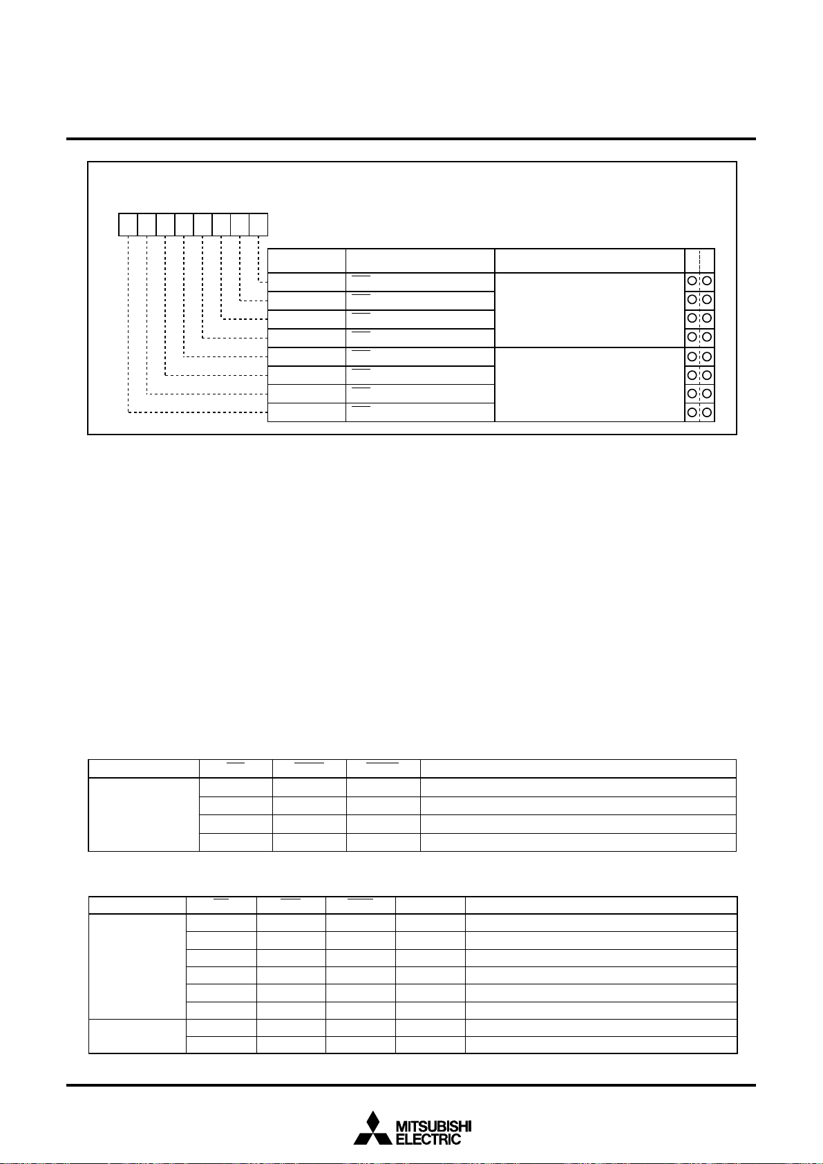
SINGLE-CHIP 16-BIT CMOS MICROCOMPUTER with CLOSED CAPTION DECODER
Chip select control register
b7 b6 b5 b4 b3 b2 b1 b0
MITSUBISHI MICROCOMPUTERS
M306V2ME-XXXFP
and ON-SCREEN DISPLAY CONTROLLER
Symbol Address When reset
CSR 0008
16
01
16
M306V2EEFP
Bit symbol
CS0
CS1
CS2
CS3
CS0W
CS1W
CS2W
CS3W
Bit name
CS0 output enable bit
CS1 output enable bit
CS2 output enable bit
CS3 output enable bit
CS0 wait bit
CS1 wait bit
CS2 wait bit
CS3 wait bit
0 : Chip select output disabled
(Normal port pin)
1 : Chip select output enabled
0 : Wait state inserted
1 : No wait state
Function
Figure 2.4.4 Chip select control register
(3) Read/write signals
With a 16-bit data bus (BYTE pin =“L”), bit 2 of the processor mode register 0 (address 000416) select
the combinations of RD, BHE, and WR signals or RD, WRL, and WRH signals. With an 8-bit data bus
_____ ________ ______ _____ ________ _________
_____ ______ _______
(BYTE pin = “H”), use the combination of RD, WR, and BHE signals. (Set bit 2 of the processor mode
register 0 (address 000416) to “0”.) Tables 2.4.4 and 2.4.5 show the operation of these signals.
_____ ______ ________
After a reset has been cancelled, the combination of RD, WR, and BHE signals is automatically selected.
_____ _________ _________
When switching to the RD, WRL, and WRH combination, do not write to external memory until bit 2 of
the processor mode register 0 (address 000416) has been set (Note).
W
R
Note: Before attempting to change the contents of the processor mode register 0, set bit 1 of
the protect register (address 000A16) to “1”.
Table 2.4.4 Operation of RD, WRL, and WRH signals
_____ ________ _________
Data bus width
16-bit
(BYTE = “L”)
L
H
H
H
_____ ______ ________
H
L
H
L
WRHWRLRD
H
H
L
L
Read data
Write 1 byte of data to even address
Write 1 byte of data to odd address
Write data to both even and odd addresses
Status of external data bus
Table 2.4.5 Operation of RD, WR, and BHE signals
Data bus width A0
16-bit
(BYTE = “L”)
RD
BHEWR
HLL
LHL
HLH
LHH
H
H
HLLL
LHLL
8-bit
(BYTE = “H”)
H L H / L
L H H / L
Not used
Not used
Write 1 byte of data to odd address
Read 1 byte of data from odd address
L
L
Write 1 byte of data to even address
Read 1 byte of data from even address
Write data to both even and odd addresses
Read data from both even and odd addresses
Write 1 byte of data
Read 1 byte of data
Status of external data bus
30
Rev. 1.0

MITSUBISHI MICROCOMPUTERS
M306V2ME-XXXFP
M306V2EEFP
SINGLE-CHIP 16-BIT CMOS MICROCOMPUTER with CLOSED CAPTION DECODER
and ON-SCREEN DISPLAY CONTROLLER
(4) ALE signal
The ALE signal latches the address when accessing the multiplex bus space. Latch the address when
the ALE signal falls.
When BYTE pin = “H”
ALE
D
0/A0
to D7/A
A8 to A
7
19
Address Data (Note 1)
Address (Note 2)
Notes 1: Floating when reading.
2: When multiplexed bus for the entire space is selected, these are I/O ports.
Figure 2.4.5 ALE signal and address/data bus
D
When BYTE pin = “L”
ALE
A
0
0/A1
to D7/A
A9 to A
8
19
Address
Address Data (Note 1)
Address
Rev. 1.0
31

MITSUBISHI MICROCOMPUTERS
M306V2ME-XXXFP
M306V2EEFP
SINGLE-CHIP 16-BIT CMOS MICROCOMPUTER with CLOSED CAPTION DECODER
and ON-SCREEN DISPLAY CONTROLLER
________
(5) RDY signal
________
RDY signal facilitates access of external devices that require a long time for access. As shown in
Figure 2.4.6, if an “L” is being input to the RDY pin at the BCLK falling edge, the bus turns to the wait
state. If an “H” is being input to the RDY pin at the BCLK falling edge, the bus cancels the wait state.
Table 2.4.6 shows the microcomputer state in the wait state. Figure 2.4.6 shows the example of the
_____ ________
RD signal being extended using the RDY signal.
________
The RDY signal is valid when accessing the external area during the bus cycle in which bits 4 to 7 of
the chip select control register (address 000816) are set to “0.” The RDY signal is invalid when setting
“1” to all bits 4 to 7 of the chip select control register (address 000816), but the RDY pin should be
treated as properly as in non-using.
Table 2.4.6 Microcomputer status in ready state (Note)
Item Status
Oscillation On
___ _____
R/W signal, address bus, data bus, CS
__________
ALE signal, HLDA, programmable I/O ports
Internal peripheral circuits On
________
Note: The RDY signal cannot be received immediately prior to a software wait.
________
________
________
________
________
Maintain status when RDY signal received
In an instance of separate bus
BCLK
RD
CS
i
(i=0 to 3)
RDY
Accept timing of RDY signal
In an instance of multiplexed bus
BCLK
RD
CS
i
(i=0 to 3)
RDY
tsu(RDY - BCLK)
tsu(RDY - BCLK)
: Wait using RDY signal
: Wait using software
_____ ________
Figure 2.4.6 Example of RD signal extended by RDY signal
32
Accept timing of RDY signal
Rev. 1.0

MITSUBISHI MICROCOMPUTERS
M306V2ME-XXXFP
M306V2EEFP
SINGLE-CHIP 16-BIT CMOS MICROCOMPUTER with CLOSED CAPTION DECODER
and ON-SCREEN DISPLAY CONTROLLER
(6) Hold signal
The hold signal is used to transfer the bus privileges from the CPU to the external circuits. Inputting “L”
__________
to the HOLD pin places the microcomputer in the hold state at the end of the current bus access. This
status is maintained and “L” is output from the HLDA pin as long as “L” is input to the HOLD pin. Table
2.4.7 shows the microcomputer status in the hold state.
__________
Bus-using priorities are given to HOLD, DMAC, and CPU in order of decreasing precedence.
__________
HOLD > DMAC > CPU
Figure 2.4.7 Bus-using priorities
Table 2.4.7 Microcomputer status in hold state
Item Status
Oscillation ON
___ _____ _______
R/W signal, address bus, data bus, CS, BHE Floating
Programmable I/O ports P0, P1, P2, P3, P4, P5 Floating
__________
HLDA Output “L”
Internal peripheral circuits ON (but watchdog timer stops)
ALE signal Undefined
P6, P7, P8, P9, P10 Maintains status when hold signal is received
__________ __________
(7) External bus status when internal area is accessed
Table 2.4.8 shows the external bus status when the internal area is accessed.
Table 2.4.8 External bus status when the internal area is accessed
Item SFR accessed Internal ROM/RAM accessed
Address bus Address output Maintain status before accessed
address of external area
Data bus When read Floating Floating
When write Output data Undefined
RD, WR, WRL, WRH RD, WR, WRL, WRH output Output "H"
BHE BHE output Maintain status before accessed
status of external area
CS Output "H" Output "H"
ALE Output "L" Output "L"
(8) BCLK output
The output of the internal clock φ can be selected using bit 7 of the processor mode register 0 (address
000416) (Note). The output is floating when bit 7 is set to “1”.
Rev. 1.0
Note: Before attempting to change the contents of the processor mode register 0, set bit 1 of the
protect register (address 000A16) to “1”.
33

MITSUBISHI MICROCOMPUTERS
M306V2ME-XXXFP
M306V2EEFP
SINGLE-CHIP 16-BIT CMOS MICROCOMPUTER with CLOSED CAPTION DECODER
and ON-SCREEN DISPLAY CONTROLLER
(9) Software wait
A software wait can be inserted by setting the wait bit (bit 7) of the processor mode register 1 (address
000516) (Note) and bits 4 to 7 of the chip select control register (address 000816).
A software wait is inserted in the internal ROM/RAM area and in the external memory area by setting
the wait bit of the processor mode register 1. When set to “0”, each bus cycle is executed in one BCLK
cycle. When set to “1”, each bus cycle is executed in two or three BCLK cycles. After the microcomputer has been reset, this bit defaults to “0”. When set to “1”, a wait is applied to all memory areas (two
or three BCLK cycles), regardless of the contents of bits 4 to 7 of the chip select control register. Set
this bit after referring to the recommended operating conditions (main clock input oscillation frequency) of the electric characteristics. However, when the user is using the RDY signal, the relevant
bit in the chip select control register’s bits 4 to 7 must be set to “0.”
When the wait bit of the processor mode register 1 is “0”, software waits can be set independently for
each of the 4 areas selected using the chip select signal. Bits 4 to 7 of the chip select control register
_______ _______
correspond to chip selects CS0 to CS3. When one of these bits is set to “1”, the bus cycle is executed
in one BCLK cycle. When set to “0”, the bus cycle is executed in two or three BCLK cycles. These bits
default to “0” after the microcomputer has been reset. These bits default to “0” after the microcomputer
has been reset.
The SFR area and the OSD RAM area are always accessed in two BCLK cycles regardless of the
setting of these control bits. Also, the corresponding bits of the chip select control register must be set
to “0” if using the multiplex bus to access the external memory area.
Table 2.4.9 shows the software wait and bus cycles. Figure 2.4.8 shows example bus timing when
using software waits.
Note: Before attempting to change the contents of the processor mode register 1, set bit 1 of the
protect register (address 000A16) to “1”.
________
Table 2.4.9 Software waits and bus cycles
Area Bus status Wait bit
SFR/
OSD RAM
Internal
ROM/RAM
Separate bus
External
memory
area
Note: When using the RDY signal, always set to “0.”
34
Separate bus
Separate bus
Multiplex bus 0 0 3 BCLK cycles
Multiplex bus
Invalid Invalid 2 BCLK cycles
Bits 4 to 7 of chip select
control register
0 Invalid 1 BCLK cycle
Invalid1 2 BCLK cycles
0 1 1 BCLK cycle
0 0 2 BCLK cycles
1 0 (Note) 2 BCLK cycles
1 3 BCLK cycles0 (Note)
Bus cycle
Rev. 1.0

MITSUBISHI MICROCOMPUTERS
M306V2ME-XXXFP
M306V2EEFP
SINGLE-CHIP 16-BIT CMOS MICROCOMPUTER with CLOSED CAPTION DECODER
and ON-SCREEN DISPLAY CONTROLLER
< Separate bus (no wait) >
BCLK
Write signal
Read signal
Data bus
Address bus
Chip select
< Separate bus (with wait) >
BCLK
Write signal
Read signal
Bus cycle
Address
Bus cycle
Output
Input
Address
Data bus
Address bus
Chip select
< Multiplexed bus >
Write signal
Read signal
Address bus
Address bus/
Data bus
Chip select
BCLK
ALE
Address
Address
Bus cycle
Address
Data output
Output
Address
Input
Address
Address
Input
Figure 2.4.8 Typical bus timings using software wait
Rev. 1.0
35

MITSUBISHI MICROCOMPUTERS
M306V2ME-XXXFP
M306V2EEFP
SINGLE-CHIP 16-BIT CMOS MICROCOMPUTER with CLOSED CAPTION DECODER
and ON-SCREEN DISPLAY CONTROLLER
2.5 Clock Generating Circuit
The clock generating circuit contains 2 oscillator circuits that supply the operating clock sources to the CPU
and internal peripheral units and 1 oscillator circuit that supplies the operating clock source to OSD.
Table 2.5.1. Clock oscillation circuits
Main clock oscillation circuit Sub-clock oscillation circuit OSD oscillation circuit
Use of clock • CPU’s operating clock • CPU’s operating clock • OSD’s operating clock
source source source
• Internal peripheral units’ • Timer A/B’s count clock
operating clock source source
Usable oscillator
Pins to connect XIN, XOUT XIN, XOUT OSC1, OSC2
oscillator
Oscillation stop/restart Available Available
function
Oscillator status Oscillating Stopped
immediately after reset
Other Externally derived clock can be input
•Ceramic resonator •Quartz-crystal oscillator •Ceramic resonator
(or quartz-crystal oscillator) (or quartz-crystal oscillator)
•LC oscillator
36
Rev. 1.0

MITSUBISHI MICROCOMPUTERS
O
C
C
O
C
C
M306V2ME-XXXFP
M306V2EEFP
SINGLE-CHIP 16-BIT CMOS MICROCOMPUTER with CLOSED CAPTION DECODER
and ON-SCREEN DISPLAY CONTROLLER
2.5.1 Example of Oscillator Circuit
Figure 2.5.1 shows some examples of the main clock circuit, one using an oscillator connected to the
circuit, and the other one using an externally derived clock for input. Figure 2.5.2 shows some examples
of sub-clock circuits, one using an oscillator connected to the circuit, and the other one using an externally
derived clock for input. Circuit constants in Figures 2.5.1 and 2.5.2 vary with each oscillator used. Use
the values recommended by the manufacturer of your oscillator.
M i c r o c o m p u t e r
( B u i l t - i n f e e d b a c k r e s i s t o r )
X
I N
I N
N o t e : I n s e r t a d a m p i n g r e s i s t o r i f r e q u i r e d . T h e r e s i s t a n c e w i l l v a r y d e p e n d i n g o n t h e o s c i l l a t o r a n d t h e o s c i l l a t i o n d r i v e
c a p a c i t y s e t t i n g . U s e t h e v a l u e r e c o m m e n d e d b y t h e m a k e r o f t h e o s c i l l a t o r .
W h e n t h e o s c i l l a t i o n d r i v e c a p a c i t y i s s e t t o l o w , c h e c k t h a t o s c i l l a t i o n i s s t a b l e . W h e n b e i n g s p e c i f i e d t o c o n n e c t a
f e e d b a c k r e s i s t o r e x t e r n a l l y b y t h e m a n u f a c t u r e , c o n n e c t a f e e d b a c k r e s i s t o r b e t w e e n p i n s X
X
O U T
( N o t e )
R
d
O U T
Figure 2.5.1 Examples of main clock
M i c r o c o m p u t e r
( B u i l t - i n f e e d b a c k r e s i s t o r )
X
C I N
C I N
N o t e : I n s e r t a d a m p i n g r e s i s t o r i f r e q u i r e d . T h e r e s i s t a n c e w i l l v a r y d e p e n d i n g o n t h e o s c i l l a t o r a n d t h e o s c i l l a t i o n d r i v e
c a p a c i t y s e t t i n g . U s e t h e v a l u e r e c o m m e n d e d b y t h e m a k e r o f t h e o s c i l l a t o r .
W h e n t h e o s c i l l a t i o n d r i v e c a p a c i t y i s s e t t o l o w , c h e c k t h a t o s c i l l a t i o n i s s t a b l e . W h e n b e i n g s p e c i f i e d t o c o n n e c t a
f e e d b a c k r e s i s t o r e x t e r n a l l y b y t h e m a n u f a c t u r e , c o n n e c t a f e e d b a c k r e s i s t o r b e t w e e n p i n s X
X
C O U T
( N o t e )
R
C d
C O U T
M i c r o c o m p u t e r
( B u i l t - i n f e e d b a c k r e s i s t o r )
X
I N
E x t e r n a l l y d e r i v e d c l o c k
V c c
V s s
I N
a n d X
M i c r o c o m p u t e r
( B u i l t - i n f e e d b a c k r e s i s t o r )
X
C I N
E x t e r n a l l y d e r i v e d c l o c k
V c c
V s s
C IN
X
p e
a n d X
O U T
X
p e
O U T
C O U T
C OU T
n
.
n
.
Figure 2.5.2 Examples of sub-clock
Rev. 1.0
37

MITSUBISHI MICROCOMPUTERS
M306V2ME-XXXFP
M306V2EEFP
SINGLE-CHIP 16-BIT CMOS MICROCOMPUTER with CLOSED CAPTION DECODER
and ON-SCREEN DISPLAY CONTROLLER
2.5.2 OSD Oscillation Circuit
The OSD clock oscillation circuit can obtain simply a clock for OSD by connecting an LC oscillator or a
ceramic resonator (or a quartz-crystal oscillator) across the pins OSC1 and OSC2. Which of LC oscillator
or a ceramic resonator (or a quartz-crystal oscillator) is selected by setting bits 1 and 2 of the clock control
register (address 020516).
Microcomputer
OSC2OSC1
C1 C2
L
Figure 2.5.3 OSD clock connection example
2.5.3 Clock Control
Figure 2.5.4 shows the block diagram of the clock generating circuit.
X
CIN
X
RESET
Software reset
Interrupt request
level judgment
output
CM10 “1”
Write signal
WAIT instruction
COUT
CM04
Sub clock
QS
R
QS
R
CM05
X
IN
Main clock
X
OUT
CM02
1/32
f
C32
f
C
f
1
f
AD
f
8
f
32
c
b
a
Divider
d
f
C
CM07=1
f1SIO2
f8SIO2
f32SIO2
CM07=0
BCLK
CM0i : Bit i at address 0006
CM1i : Bit i at address 0007
WDCi : Bit i at address 000F
Figure 2.5.4 Clock generating circuit
38
b
a
16
16
16
1/2 1/2 1/2 1/2
CM06=1
CM06=0
CM17,CM16=01
CM06=0
CM17,CM16=00
CM06=0
CM17,CM16=10
CM06=0
CM17,CM16=11
Details of divider
c
1/2
d
Rev. 1.0

MITSUBISHI MICROCOMPUTERS
M306V2ME-XXXFP
M306V2EEFP
SINGLE-CHIP 16-BIT CMOS MICROCOMPUTER with CLOSED CAPTION DECODER
and ON-SCREEN DISPLAY CONTROLLER
The following paragraphs describes the clocks generated by the clock generating circuit.
(1) Main clock
The main clock is generated by the main clock oscillation circuit. After a reset, the clock is divided by
8 to the BCLK. The clock can be stopped using the main clock stop bit (bit 5 at address 000616).
Stopping the clock, after switching the operating clock source of CPU to the sub-clock, reduces the
power dissipation.
After the oscillation of the main clock oscillation circuit has stabilized, the drive capacity of the main
clock oscillation circuit can be reduced using the XIN-XOUT drive capacity select bit (bit 5 at address
000716). Reducing the drive capacity of the main clock oscillation circuit reduces the power dissipation. This bit changes to “1” when shifting from high-speed/medium-speed mode to stop mode and at
a reset. When shifting from low-speed/low power dissipation mode to stop mode, the value before
stop mode is retained.
(2) Sub-clock
The sub-clock is generated by the sub clock oscillation circuit. No sub clock is generated after a reset.
After oscillation is started using the port Xc select bit (bit 4 at address 000616), the sub-clock can be
selected as the BCLK by using the system clock select bit (bit 7 at address 000616). However, be sure
that the sub-clock oscillation has fully stabilized before switching.
After the oscillation of the sub-clock oscillation circuit has stabilized, the drive capacity of the sub-clock
oscillation circuit can be reduced using the XCIN-XCOUT drive capacity select bit (bit 3 at address
000616). Reducing the drive capacity of the sub-clock oscillation circuit reduces the power dissipation.
This bit changes to “1” when shifting to stop mode and at a reset.
(3) BCLK
The internal clock φ is the clock that drives the CPU, and is fc or the clock derived by dividing the main
clock by 1, 2, 4, 8, or 16. The BCLK is derived by dividing the main clock by 8 after a reset. The BCLK
signal can be output from pin BCLK by the BCLK output disable bit (bit 7 at address 000416) in the
memory expansion and the microprocessor modes.
The main clock division select bit 0 (bit 6 at address 000616) changes to “1” when shifting from highspeed/medium-speed to stop mode and at reset. When sifting from low-speed/low power dissipation
mode to stop mode, the value before stop mode is retained.
(4) Peripheral function clock (f1, f8, f32, f1SIO2, f8SIO2, f32SIO2, fAD)
The clock for the peripheral devices is derived by dividing the main clock by 1, 8 or 32. The peripheral
function clock is stopped by stopping the main clock or by setting the WAIT peripheral function clock
stop bit (bit 2 at 000616) to “1” and then executing a WAIT instruction.
(5) fC32
This clock is derived by dividing the sub-clock by 32. It is used for the timer A and timer B counts.
(6) fC
This clock has the same frequency as the sub-clock. It is used for the BCLK and for the watchdog
timer.
Rev. 1.0
39

MITSUBISHI MICROCOMPUTERS
)
SINGLE-CHIP 16-BIT CMOS MICROCOMPUTER with CLOSED CAPTION DECODER
and ON-SCREEN DISPLAY CONTROLLER
Figures 2.5.5 and 2.5.6 shows the system clock control registers 0 and 1.
S y s t e m c l o c k c o n t r o l r e g i s t e r 0 ( N o t e 1 )
d d r e s
b 7b 6b 5b 4b 3b 2b 1b 0
N o t e s 1 : S e t b i t 0 o f t h e p r o t e c t r e g i s t e r ( a d d r e s s 0 0 0 A
2 : C h a n g e s t o “ 1 ” w h e n s h i f t i n g t o s t o p m o d e a n d a t a r e s e t .
3 : W h e n e n t e r i n g p o w e r s a v i n g m o d e , m a i n c l o c k s t o p s u s i n g t h i s . W h e n r e t u r n i n g f r o m s t o p m o d e a n d
o p e r a t i n g w i t h X
b i t ( C M 0 7 ) t o “ 1 ” b e f o r e s e t t i n g t h i s b i t t o “ 1 ” .
4 : W h e n i n p u t t i n g e x t e r n a l c l o c k , o n l y c l o c k o s c i l l a t i o n b u f f e r i s s t o p p e d a n d c l o c k i n p u t i s a c c e p t a b l e .
5 : I f t h i s b i t i s s e t t o “ 1 , ” X
p u l l e d u p t o X
6 : S e t p o r t X c s e l e c t b i t ( C M 0 4 ) t o “ 1 ” a n d s t a b i l i z e t h e s u b - c l o c k o s c i l l a t i n g b e f o r e s e t t i n g t o t h i s b i t f r o m “ 0 ” t o
“ 1 . ” D o n o t w r i t e t o b o t h b i t s a t t h e s a m e t i m e . A n d a l s o , s e t t h e m a i n c l o c k s t o p b i t ( C M 0 5 ) t o “ 0 ” a n d s t a b i l i z e
t h e m a i n c l o c k o s c i l l a t i n g b e f o r e s e t t i n g t h i s b i t f r o m “ 1 ” t o “ 0 . ”
7: T h i s b i t c h a n g e s t o “ 1 ” w h e n s h i f t i n g f r o m h i g h - s p e e d / m e d i u m - s p e e d m o d e t o s t o p m o d e a n d a t a r e s e t . W h e n
s h i f t i n g f r o m l o w - s p e e d / l o w p o w e r d i s s i p a t i o n m o d e t o s t o p m o d e , t h e v a l u e b e f o r e s t o p m o d e i s r e t a i n e d .
C 3 2
i s n o t i n c l u d e d .
8: f
0 0
S y m b o lA
C M 00
B i t n a m eF
C l o c k o u t p u t f u n c t i o n
C M 0 0
s e l e c t b i t
( V a l i d o n l y i n s i n g l e - c h i p
C M 0 1
m o d e )
W A I T p e r i p h e r a l f u n c t i o n
C M 0 2
c l o c k s t o p b i t
X
C I N
- X
C M 0 3
C M 0 4
C M 0 5
C M 0 6
C M 0 7
I N
, s e t t h i s b i t t o “ 0 . ” W h e n m a i n c l o c k o s c i l l a t i o n i s o p e r a t i n g b y i t s e l f , s e t s y s t e m c l o c k s e l e c t
O U T
O U T
( “ H ” ) v i a t h e f e e d b a c k r e s i s t o r .
C O U T
s e l e c t b i t ( N o t e 2 )
P o r t XC s e l e c t b i t0
M a i n c l o c k ( X
s t o p b i t ( N o t e s 3 , 4 , 5 )
M a i n c l o c k d i v i s i o n s e l e c t
b i t 0 ( N o t e 7 )
S y s t e m c l o c k s e l e c t b i t
( N o t e 6)
t u r n s “ H . ” T h e b u i l t - i n f e e d b a c k r e s i s t o r r e m a i n s b e i n g c o n n e c t e d , s o X
sW h e n r e s e t
6
1 6
d r i v e c a p a c i t y
I N
- X
O U T
1 6
4 8
1 6
b 1 b 0
0 0 : I / O p o r t P 5
0 1 : fC o u t p u t
1 0 : f
8
o u t p u t
1 1 : f
3 2
o u t p u t
0 : D o n o t s t o p p e r i p h e r a l f u n c t i o n c l o c k i n w a i t m o d e
1 : S t o p p e r i p h e r a l f u n c t i o n c l o c k i n w a i t m o d e ( N o t e 8 )
0 : L O W
1 : H I G H
: I / O p o r t
C I N
- X
C O U T
1 : X
)
0 : O n
1 : O f f
0 : C M 1 6 a n d C M 1 7 v a l i d
1 : D i v i s i o n b y 8 m o d e
I N
, X
O U T
0 : X
1 : X
C I N
, X
C O U T
) t o “ 1 ” b e f o r e w r i t i n g t o t h i s r e g i s t e r .
u n c t i o
7
g e n e r a t i o n
nB i t s y m b o l
M306V2ME-XXXFP
M306V2EEFP
WR
I N
t u r n s
Figures 2.5.5 System clock control register 0
S y s t e m c l o c k c o n t r o l r e g i s t e r 1 ( N o t e 1 )
b 7b 6b 5b 4b 3b 2b 1b 0
00
00
N o t e s 1 : S e t b i t 0 o f t h e p r o t e c t r e g i s t e r ( a d d r e s s 0 0 0 A
2 : T h i s b i t c h a n g e s t o “ 1 ” w h e n s h i f t i n g f r o m h i g h - s p e e d / m e d i u m - s p e e d m o d e t o s t o p m o d e a n d a t a
r e s e t . W h e n s h i f t i n g f r o m l o w - s p e e d / l o w p o w e r d i s s i p a t i o n m o d e t o s t o p m o d e , t h e v a l u e b e f o r e s t o p
m o d e i s r e t a i n e d .
3 : C a n b e s e l e c t e d w h e n b i t 6 o f t h e s y s t e m c l o c k c o n t r o l r e g i s t e r 0 ( a d d r e s s 0 0 0 6
I f
“ 1 ” , d i v i s i o n m o d e i s f i x e d a t 8 .
4 : I f t h i s b i t i s s e t t o “ 1 , ” X
h i g h - i m p e d a n c e s t a t e .
d d r e s
0 0
S y m b o lA
C M 10
C M 1 0
R e s e r v e d b i t s
C M 1 5
C M 1 6
C M 1 7
A l l c l o c k s t o p c o n t r o l b i t
X
I N
- X
O U T
s e l e c t b i t ( N o t e 2 )
M a i n c l o c k d i v i s i o n
s e l e c t b i t 1 ( N o t e 3 )
O U T
t u r n s “ H , ” a n d t h e b u i l t - i n f e e d b a c k r e s i s t o r i s c u t o f f . X
sW h e n r e s e t
1 6
7
B i t n a m eF
( N o t e 4
d r i v e c a p a c i t y
1 6
) t o “ 1 ” b e f o r e w r i t i n g t o t h i s r e g i s t e r .
2 0
1 6
u n c t i o
nB i t s y m b o l
0 : C l o c k o n
1 : A l l c l o c k s o f f ( s t o p m o d e )
M u s t a l w a y s b e s e t t o
0 : L O W
1 : H I G H
b 7 b 6
0 0 : N o d i v i s i o n m o d e
0 1 : D i v i s i o n b y 2 m o d e
1 0 : D i v i s i o n b y 4 m o d e
1 1 : D i v i s i o n b y 1 6 m o d e
“ 0 ”
1 6
) i s “ 0 . ”
C IN
an d X
C OU T
WR
t u r n
Figure 2.5.6 System clock control register 1
40
Rev. 1.0

MITSUBISHI MICROCOMPUTERS
M306V2ME-XXXFP
M306V2EEFP
SINGLE-CHIP 16-BIT CMOS MICROCOMPUTER with CLOSED CAPTION DECODER
and ON-SCREEN DISPLAY CONTROLLER
2.5.4 Clock Output
In single-chip mode, the clock output function select bits (bits 0 and 1 at address 000616) enable f8, f32, or
fc to be output from the P57/CLKOUT pin. When the WAIT peripheral function clock stop bit (bit 2 at
address 000616) is set to “1,” the output of f8 and f32 stops when a WAIT instruction is executed.
2.5.5 Stop Mode
Writing “1” to the all-clock stop control bit (bit 0 at address 000716) stops all oscillation and the microcomputer enters stop mode. In stop mode, the content of the internal RAM is retained provided that VCC
remains above 4.5V.
Because the oscillation, BCLK, f1 to f32, f1SIO2 to f32SIO2, fC, fC32, and fAD stops in stop mode, peripheral
functions such as the A-D converter and watchdog timer do not function. However, timer B operates
provided that the event counter mode is set to an external pulse, and UARTi (i = 0, 2) functions provided
an external clock is selected. Table 2.5.2 shows the status of the ports in stop mode.
Stop mode is cancelled by a hardware reset or an interrupt. If an interrupt is to be used to cancel stop
mode, that interrupt must first have been enabled. If returning by an interrupt, that interrupt routine is
executed.
When shifting from high-speed/medium-speed mode to stop mode and at a reset, the main clock division
select bit 0 (bit 6 at address 000616) is set to “1.” When shifting from low-speed/low power dissipation
mode to stop mode, the value before stop mode is retained.
Table 2.5.2 Port status during stop mode
Pin Memory expansion mode Single-chip mode
Microprocessor mode
Address bus, data bus, CS0 to CS3
_____ ______ ________ ________ _________
_______ _______
Retains status before stop mode
RD, WR, BHE, WRL, WRH “H”
__________
HLDA, BCLK “H”
ALE “H”
Port
Retains status before stop mode
CLKOUT When fc selected Valid only in single-chip mode “H”
When f8, f32 selected Valid only in single-chip mode
Retains status before stop mode
Retains status before stop mode
Rev. 1.0
41

MITSUBISHI MICROCOMPUTERS
M306V2ME-XXXFP
M306V2EEFP
SINGLE-CHIP 16-BIT CMOS MICROCOMPUTER with CLOSED CAPTION DECODER
and ON-SCREEN DISPLAY CONTROLLER
2.5.6 Wait Mode
When a WAIT instruction is executed, the BCLK stops and the microcomputer enters the wait mode. In
this mode, oscillation continues but the BCLK and watchdog timer stop. Writing “1” to the WAIT peripheral
function clock stop bit and executing a WAIT instruction stops the clock being supplied to the internal
peripheral functions, allowing power dissipation to be reduced. Table 2.5.3 shows the status of the ports
in wait mode.
Wait mode is cancelled by a hardware reset or an interrupt. If an interrupt is used to cancel wait mode, the
microcomputer restarts from the interrupt routine using as BCLK, the clock that had been selected when
the WAIT instruction was executed.
Table 2.5.3 Port status during wait mode
Pin Memory expansion mode Single-chip mode
Microprocessor mode
Address bus, data bus, CS0 to CS3
_____ ______ ________ ________ _________
_______ _______
Retains status before wait mode
RD, WR, BHE, WRL, WRH “H”
__________
HLDA,BCLK “H”
ALE “H”
Port
Retains status before wait mode Retains status before wait mode
CLKOUT When fC selected Valid only in single-chip mode Does not stop
When f8, f32 selected Valid only in single-chip mode Does not stop when the WAIT
peripheral function clock stop
bit is “0”.
When the WAIT peripheral
function clock stop bit is “1”,
the status immediately prior
to entering wait mode is maintained.
42
Rev. 1.0

MITSUBISHI MICROCOMPUTERS
M306V2ME-XXXFP
M306V2EEFP
SINGLE-CHIP 16-BIT CMOS MICROCOMPUTER with CLOSED CAPTION DECODER
and ON-SCREEN DISPLAY CONTROLLER
2.5.7 Status Transition of BCLK
Power dissipation can be reduced and low-voltage operation achieved by changing the count source for
BCLK. Table 2.5.4 shows the operating modes corresponding to the settings of system clock control
registers 0 and 1.
After a reset, operation defaults to division by 8 mode. When shifting to stop mode, the main clock division
select bit 0 (bit 6 at address 000616) is set to “1”. The following shows the operational modes of internal
clock φ.
(1) Division by 2 mode
The main clock is divided by 2 to obtain the BCLK.
(2) Division by 4 mode
The main clock is divided by 4 to obtain the BCLK.
(3) Division by 8 mode
The main clock is divided by 8 to obtain the BCLK. Note that oscillation of the main clock must have
stabilized before transferring from this mode to another mode.
(4) Division by 16 mode
The main clock is divided by 16 to obtain the BCLK.
(5) No-division mode
The main clock is used as the BCLK.
(6) Low-speed mode
fC is used as the BCLK. Note that oscillation of both the main and sub clocks must have stabilized
before transferring from this mode to another or vice versa. At least 2 to 3 seconds are required after
the sub clock starts. Therefore, the program must be written to wait until this clock has stabilized
immediately after powering up and after stop mode is cancelled.
(7) Low power dissipation mode
fC is the BCLK and the main clock is stopped.
Note: When switching the count source for BCLK between XIN and XCIN, it needs that the oscillation of
the switched count source is sufficiently stable. Shift after taking the oscillation stabilizing time by
software.
Table 2.5.4 Operating modes dictated by settings of system clock control registers 0 and 1
CM17 CM16 CM07 CM06 CM05 CM04 Operating mode of BCLK
01000Invalid Division by 2 mode
10000Invalid Division by 4 mode
Invalid Invalid 0 1 0 Invalid Division by 8 mode
11000Invalid Division by 16 mode
00000Invalid No-division mode
Invalid Invalid 1 Invalid 0 1 Low-speed mode
Invalid Invalid 1 Invalid 1 1 Low power dissipation mode
Rev. 1.0
43

MITSUBISHI MICROCOMPUTERS
M306V2ME-XXXFP
M306V2EEFP
SINGLE-CHIP 16-BIT CMOS MICROCOMPUTER with CLOSED CAPTION DECODER
and ON-SCREEN DISPLAY CONTROLLER
2.5.8 Power Control
The following is a description of the three available power control modes:
Modes
Power control is available in three modes.
(1) Normal operation mode
■ High-speed mode
Divide-by-1 frequency of the main clock becomes the BCLK. The CPU operates with the internal
clock selected. Each peripheral function operates according to its assigned clock.
■ Medium-speed mode
Divide-by-2, divide-by-4, divide-by-8, or divide-by-16 frequency of the main clock becomes the
BCLK. The CPU operates according to the internal clock selected. Each peripheral function operates
according to its assigned clock.
■ Low-speed mode
fC becomes the BCLK. The CPU operates according to the fc clock. The fc clock is supplied by the
secondary clock. Each peripheral function operates according to its assigned clock.
■ Low power consumption mode
The main clock operating in low-speed mode is stopped. The CPU operates according to the fc
clock. The fc clock is supplied by the secondary clock. The only peripheral functions that operate are
those with the sub-clock selected as the count source.
(2) Wait mode
The CPU operation is stopped. The oscillators do not stop.
(3) Stop mode
All oscillators stop. The CPU and all built-in peripheral functions stop. This mode, among the three
modes listed here, is the most effective in decreasing power consumption.
Figure 2.5.7 is the state transition diagram of the above modes.
44
Rev. 1.0

SINGLE-CHIP 16-BIT CMOS MICROCOMPUTER with CLOSED CAPTION DECODER
T r a n s i t i o n o f s t o p m o d e , w a i t m o d e
S t o p m o d e
A l l o s c i l l a t o r s s t o p p e d
S t o p m o d e
A l l o s c i l l a t o r s s t o p p e d
S t o p m o d e
A l l o s c i l l a t o r s s t o p p e d
C M 1 0 = “ 1 ”
I n t e r r u p t
I n t e r r u p t
C M 1 0 = “ 1 ”
C M 1 0 = “ 1 ”
I n t e r r u p t
M e d i u m - s p e e d m o d e
( D i v i d e d - b y - 8 m o d e )
m e d i u m - s p e e d
l o w p o w e r d i s s i p a t i o n
N o r m a l m o d e
( S e e t h e f i g u r e b e l o w a s f o r t r a n s i t i o n o f n o r m a l m o d e )
T r a n s i t i o n o f n o r m a l m o d e
M a i n c l o c k i s o s c i l l a t i n g
S u b - c l o c k i s s t o p p e d
M e d i u m - s p e e d m o d e ( d i v i d e d - b y - 8 m o d e )
C M 0 6 = “ 1 ”
M a i n c l o c k i s o s c i l l a t i n g
S u b - c l o c k i s o s c i l l a t i n g
H i g h - s p e e d m o d e
B C L K : f ( X
I N
C M 0 7 = “ 0 ” C M 0 6 = “ 0 ”
C M 1 7 = “ 0 ” C M 1 6 = “ 0 ”
B C L K : f ( X
C M 0 7 = “ 0 ” C M 0 6 = “ 0 ”
C M 1 7 = “ 1 ” C M 1 6 = “ 0 ”
C M 0 4 = “ 0 ”
H i g h - s p e e d m o d eM
B C L K : f ( X
C M 0 7 = “ 0 ” C M 0 6 = “ 0 ”
C M 1 7 = “ 0 ” C M 1 6 = “ 0 ”
)
I N
) / 4
M a i n c l o c k i s o s c i l l a t i n g
S u b c l o c k i s s t o p p e d
I N
)
B C L K : f ( X
C M 0 7 = “ 0 ”C M 0 6 = “ 1 ”
C M 0 4 = “ 0 ” C M 0 4 = “ 1 ”
M e d i u m - s p e e d m o d e ( d i v i d e d - b y - 2 )
C M 0 7 = “ 0 ” C M 0 6 = “ 0 ”
C M 1 7 = “ 0 ” C M 1 6 = “ 1 ”
M e d i u m - s p e e d m o d e ( d i v i d e d - b y - 1 6 )M e d i u m - s p e e d m o d e ( d i v i d e d - b y - 4 )
C M 0 7 = “ 0 ” C M 0 6 = “ 0 ”
C M 1 7 = “ 1 ” C M 1 6 = “ 1 ”
e d i u m - s p e e d m o d e ( d i v i d e d - b y - 2
C M 0 7 = “ 0 ” C M 0 6 = “ 0 ”
C M 1 7 = “ 0 ” C M 1 6 = “ 1 ”
R e s e t
H i g h - s p e e d /
m o d e
Lo w - s p e e d /
m o d e
B C L K : f ( X
B C L K : f ( X
C M 0 4 = “ 1 ”
B C L K : f ( X
I N
) / 8
I N
( N o t e s 1 , 3 )
I N
) / 2
I N
) / 1 6
) / 2
W A I T
i n s t r u c t i o n
W a i t m o d e
I n t e r r u p t
W A I T
i n s t r u c t i o n
C P U o p e r a t i o n s t o p p e d
W a i t m o d e
I n t e r r u p t
W A I T
i n s t r u c t i o n
C P U o p e r a t i o n s t o p p e d
W a i t m o d e
I n t e r r u p t
)
C P U o p e r a t i o n s t o p p e d
C M 0 7 = “ 0 ”
C M 0 6 = “ 1 ”
C M 0 4 = “ 0 ”
( N o t e 1 )
M e d i u m - s p e e d m o d e ( d i v i d e d - b y - 8 )
B C L K : f ( X
C M 0 7 = “ 0 ”
C M 0 6 = “ 1 ”
C M 0 7 = “ 0 ”
C M 0 6 = “ 0 ”
C M 0 4 = “ 0 ”
( N o t e s 1 , 3 )
MITSUBISHI MICROCOMPUTERS
M306V2ME-XXXFP
M306V2EEFP
and ON-SCREEN DISPLAY CONTROLLER
M a i n c l o c k i s o s c i l l a t i n g
S u b - c l o c k i s o s c i l l a t i n g
C M 0 7 = “ 0 ”
( N o t e s 1 , 3 )
I N
) / 8
C M 0 7 = “ 1 ”
( N o t e 2 )
C M 0 5 = “ 0 ” C M 0 5 = “ 1 ”
C M 0 7 = “ 1 ”
C M 0 5 = “ 1 ”
( N o t e 2 )
L o w - s p e e d m o d e
B C L K : f ( X
C I N
)
C M 0 7 = “ 1 ”
M a i n c l o c k i s s t o p p e d
S u b - c l o c k i s o s c i l l a t i n g
L o w p o w e r d i s s i p a t i o n m o d e
B C L K : f ( X
C IN
C M 0 7 = “ 1 ”
)
C M 0 6 = “ 0 ”
( N o t e s 1 , 3 )
B C L K : f ( X
I N
C M 0 7 = “ 0 ” C M 0 6 = “ 0 ”
C M 1 7 = “ 1 ” C M 1 6 = “ 0 ”
) / 4
M e d i u m - s p e e d m o d e ( d i v i d e d - b y - 1 6 )M e d i u m - s p e e d m o d e ( d i v i d e d - b y - 4 )
B C L K : f ( X
C M 0 7 = “ 0 ” C M 0 6 = “ 0 ”
C M 1 7 = “ 1 ” C M 1 6 = “ 1 ”
I N
) / 1 6
Figure 2.5.7 State transition diagram of Power control mode
Rev. 1.0
N o t e s 1 : S w i t c h c l o c k s a f t e r o s c i l l a t i o n o f m a i n c l o c k i s
s u f f i c i e n t l y s t a b l e .
2: S w i t c h c l o c k s a f t e r o s c i l l a t i o n o f s u b - c l o c k i s
s u f f i c i e n t l y s t a b l e .
3 : C h a n g e C M 0 6 a f t e r c h a n g i n g C M 1 7 a n d
C M 1 6 .
4: T r a n s i t i n a c c o r d a n c e w i t h a r r o w s .
45

MITSUBISHI MICROCOMPUTERS
y
M306V2ME-XXXFP
M306V2EEFP
SINGLE-CHIP 16-BIT CMOS MICROCOMPUTER with CLOSED CAPTION DECODER
and ON-SCREEN DISPLAY CONTROLLER
2.6 Protection
The protection function is provided so that the values in important registers cannot be changed in the event
that the program runs out of control. Figure 2.6.1 shows the protect register. The values in the processor
mode register 0 (address 000416), processor mode register 1 (address 000516), system clock control register 0 (address 000616), system clock control register 1 (address 000716) and port P9 direction register
(address 03F316) can only be changed when the respective bit in the protect register is set to “1”. Therefore, important outputs can be allocated to port P9.
If, after “1” (write-enabled) has been written to the port P9 direction register write-enable bit (bit 2 at address
000A16), a value is written to any address, the bit automatically reverts to “0” (write-inhibited). However, the
system clock control registers 0 and 1 write-enable bit (bit 0 at 000A16) and processor mode register 0 and
1 write-enable bit (bit 1 at 000A16) do not automatically return to “0” after a value has been written to an
address. The program must therefore be written to return these bits to “0”.
Protect register
b7 b6 b5 b4 b3 b2 b1 b0
Figure 2.6.1 Protect register
Symbol Address When reset
PRCR 000A
PRC0
PRC1
PRC2
Nothing is assigned.
In an attempt to write to these bits, write “0.” The value, if read, turns out to be
indeterminate.
Note: Writing a value to an address after “1” is written to this bit returns the bit
to “0.” Other bits do not automatically return to “0” and they must therefore
be reset b
Enables writing to system clock
control registers 0 and 1 (addresses
0006
16
and 0007
Enables writing to processor mode
registers 0 and 1 (addresses 0004
and 0005
Enables writing to port P9 direction
register (address 03F3
(Note
16
)
the program.
16
XXXXX0002
Bit nameBit symbol
16
)
)
16
)
0 : Write-inhibited
1 : Write-enabled
0 : Write-inhibited
16
1 : Write-enabled
0 : Write-inhibited
1 : Write-enabled
Function
WR
46
Rev. 1.0

SINGLE-CHIP 16-BIT CMOS MICROCOMPUTER with CLOSED CAPTION DECODER
2.7 Interrupts
2.7.1 Type of Interrupts
Figure 2.7.1 lists the types of interrupts.
Software
Interrupt
Hardware
Special
Peripheral I/O (Note)
MITSUBISHI MICROCOMPUTERS
M306V2ME-XXXFP
M306V2EEFP
and ON-SCREEN DISPLAY CONTROLLER
Undefined instruction (UND instruction)
Overflow (INTO instruction)
BRK instruction
INT instruction
Reset
________
DBC
Watchdog timer
Single step
Address matched
Note: Peripheral I/O interrupts are generated by the peripheral functions built into the microcomputer system.
Figure 2.7.1 Classification of interrupts
• Maskable interrupt : An interrupt which can be enabled (disabled) by the interrupt enable flag
(I flag) or whose interrupt priority can be changed by priority level.
• Non-maskable interrupt : An interrupt which cannot be enabled (disabled) by the interrupt enable flag
(I flag) or whose interrupt priority cannot be changed by priority level.
Rev. 1.0
47

MITSUBISHI MICROCOMPUTERS
M306V2ME-XXXFP
M306V2EEFP
SINGLE-CHIP 16-BIT CMOS MICROCOMPUTER with CLOSED CAPTION DECODER
and ON-SCREEN DISPLAY CONTROLLER
2.7.2 Software Interrupts
A software interrupt occurs when executing certain instructions. Software interrupts are non-maskable
interrupts.
• Undefined instruction interrupt
An undefined instruction interrupt occurs when executing the UND instruction.
• Overflow interrupt
An overflow interrupt occurs when executing the INTO instruction with the overflow flag (O flag) set to
“1”. The following are instructions whose O flag changes by arithmetic:
ABS, ADC, ADCF, ADD, CMP, DIV, DIVU, DIVX, NEG, RMPA, SBB, SHA, SUB
• BRK interrupt
A BRK interrupt occurs when executing the BRK instruction.
• INT interrupt
An INT interrupt occurs when assiging one of software interrupt numbers 0 through 63 and executing
the INT instruction. Software interrupt numbers 0 through 31 are assigned to peripheral I/O interrupts,
so executing the INT instruction allows executing the same interrupt routine that a peripheral I/O
interrupt does.
The stack pointer (SP) used for the INT interrupt is dependent on which software interrupt number is
involved.
So far as software interrupt numbers 0 through 31 are concerned, the microcomputer saves the stack
pointer assignment flag (U flag) when it accepts an interrupt request. If change the U flag to “0” and
select the interrupt stack pointer (ISP), and then execute an interrupt sequence. When returning from
the interrupt routine, the U flag is returned to the state it was before the acceptance of interrupt request. So far as software numbers 32 through 63 are concerned, the stack pointer does not make a
shift.
48
Rev. 1.0

MITSUBISHI MICROCOMPUTERS
M306V2ME-XXXFP
M306V2EEFP
SINGLE-CHIP 16-BIT CMOS MICROCOMPUTER with CLOSED CAPTION DECODER
and ON-SCREEN DISPLAY CONTROLLER
2.7.3 Hardware Interrupts
Hardware interrupts are classified into two types — special interrupts and peripheral I/O interrupts.
(1) Special interrupts
Special interrupts are non-maskable interrupts.
• Reset
Reset occurs if an “L” is input to the RESET pin.
________
• DBC interrupt
This interrupt is exclusively for the debugger, do not use it in other circumstances.
• Watchdog timer interrupt
Generated by the watchdog timer.
• Single-step interrupt
This interrupt is exclusively for the debugger, do not use it in other circumstances. With the debug
flag (D flag) set to “1,” a single-step interrupt occurs after one instruction is executed.
• Address match interrupt
An address match interrupt occurs immediately before the instruction held in the address indicated
by the address match interrupt register is executed with the address match interrupt enable bit set to
“1.” If an address other than the first address of the instruction in the address match interrupt register
is set, no address match interrupt occurs. For address match interrupt, see 2.11 Address match
Interrupt.
____________
(2) Peripheral I/O interrupts
A peripheral I/O interrupt is generated by one of built-in peripheral functions. Built-in peripheral functions are dependent on classes of products, so the interrupt factors too are dependent on classes of
products. The interrupt vector table is the same as the one for software interrupt numbers 0 through
31 the INI instruction uses. Peripheral I/O interrupts are maskable interrupts.
• Bus collision detection interrupt
This is an interrupt that the serial I/O bus collision detection generates.
• DMA0 interrupt, DMA1 interrupt
These are interrupts DMA generates.
• VSYNC interrupt
VSYNC interrupt occurs if a VSYNC edge is input.
• A-D conversion interrupt
This is an interrupt that the A-D converter generates.
• UART0 transmission, UART2 transmission interrupts
These are interrupts that the serial I/O transmission generates.
• UART0 reception, UART2 reception interrupts
These are interrupts that the serial I/O reception generates.
• Multi-master I2C-BUS interface 0 and multi-master I2C-BUS interface 1 interrupts
This is an interrupt that the serial I/O transmission/reception is completed, or a STOP condition is
detected.
• Timer A0 interrupt through timer A4 interrupt
These are interrupts that timer A generates
• Timer B0 interrupt through timer B2 interrupt
These are interrupts that timer B generates.
Rev. 1.0
49

MITSUBISHI MICROCOMPUTERS
M306V2ME-XXXFP
M306V2EEFP
SINGLE-CHIP 16-BIT CMOS MICROCOMPUTER with CLOSED CAPTION DECODER
and ON-SCREEN DISPLAY CONTROLLER
________ ________
• INT0 interrupt and INT1 interrupt
______ ______
An INT interrupt occurs if either a rising edge or a falling edge or a both edge is input to the INT pin.
• OSD1 interrupt and OSD2 interrupt
These are interrupts that OSD display is completed.
• Data slicer interrupt
This is an interrupt that data slicer circuit requests.
50
Rev. 1.0

MITSUBISHI MICROCOMPUTERS
M306V2ME-XXXFP
M306V2EEFP
SINGLE-CHIP 16-BIT CMOS MICROCOMPUTER with CLOSED CAPTION DECODER
and ON-SCREEN DISPLAY CONTROLLER
2.7.4 Interrupts and Interrupt Vector Tables
If an interrupt request is accepted, a program branches to the interrupt routine set in the interrupt vector
table. Set the first address of the interrupt routine in each vector table. Figure 2.7.2 shows the format for
specifying the address.
Two types of interrupt vector tables are available — fixed vector table in which addresses are fixed and
variable vector table in which addresses can be varied by the setting.
MSB
Vector address + 0
Vector address + 1
Vector address + 2
Vector address + 3
Figure 2.7.2 Format for specifying interrupt vector addresses
(1) Fixed vector tables
The fixed vector table is a table in which addresses are fixed. The vector tables are located in an area
extending from FFFDC16 to FFFFF16. One vector table comprises four bytes. Set the first address of
interrupt routine in each vector table. Table 2.7.1 shows the interrupts assigned to the fixed vector
tables and addresses of vector tables.
Table 2.7.1 Interrupts assigned to the fixed vector tables and addresses of vector tables
Interrupt source Vector table addresses Remarks
Address (L) to address (H)
Undefined instruction FFFDC16 to FFFDF16 Interrupt on UND instruction
Overflow FFFE016 to FFFE316 Interrupt on INTO instruction
BRK instruction FFFE416 to FFFE716
Address match FFFE816 to FFFEB16 There is an address-matching interrupt enable bit
Single step (Note) FFFEC16 to FFFEF16 Do not use
Watchdog timer FFFF016 to FFFF316
________
DBC (Note) FFFF416 to FFFF716 Do not use
Reserved source FFFE816 to FFFEB16 Do not use
Reset FFFFC16 to FFFFF16
Note: Interrupts used for debugging purposes only.
Low address
Mid address
0 0 0 0 High address
0 0 0 0 0 0 0 0
If the vector is filled with FF16, program execution starts from
the address shown by the vector in the variable vector table
LSB
Rev. 1.0
51

MITSUBISHI MICROCOMPUTERS
M306V2ME-XXXFP
M306V2EEFP
SINGLE-CHIP 16-BIT CMOS MICROCOMPUTER with CLOSED CAPTION DECODER
and ON-SCREEN DISPLAY CONTROLLER
(2) Variable vector tables
The fixed vector table is a table in which addresses are fixed. The vector tables are located in an area
extending from FFFDC16 to FFFFF16. One vector table comprises four bytes. Set the first address of
interrupt routine in each vector table. Table 2.7.2 shows the interrupts assigned to the fixed vector
tables and addresses of vector tables.
Table 2.7.2 Interrupts assigned to the variable vector tables and addresses of vector tables
S o f t w a r e i n t e r r u p t n u m b e rI
S o f t w a r e i n t e r r u p t n u m b e r 4
t o
N o t e : A d d r e s s r e l a t i v e t o a d d r e s s i n i n t e r r u p t t a b l e r e g i s t e r ( I N T B ) .
V e c t o r t a b l e a d d r e s s
A d d r e s s ( L ) t o a d d r e s s ( H )
+ 1 6 t o + 1 9 ( N o t e )
+ 2 0 t o + 2 3 ( N o t e )S o f t w a r e i n t e r r u p t n u m b e r 5
+ 2 4 t o + 2 7 ( N o t e )S o f t w a r e i n t e r r u p t n u m b e r 6
+ 2 8 t o + 3 1 ( N o t e )S o f t w a r e i n t e r r u p t n u m b e r 7
+ 3 2 t o + 3 5 ( N o t e )S o f t w a r e i n t e r r u p t n u m b e r 8
+ 3 6 t o + 3 9 ( N o t e )S o f t w a r e i n t e r r u p t n u m b e r 9
+ 4 0 t o + 4 3 ( N o t e )S o f t w a r e i n t e r r u p t n u m b e r 1 0
+ 4 4 t o + 4 7 ( N o t e ) S o f t w a r e i n t e r r u p t n u m b e r 1 1
+ 4 8 t o + 5 1 ( N o t e )S o f t w a r e i n t e r r u p t n u m b e r 1 2
+ 5 2 t o + 5 5 ( N o t e )S o f t w a r e i n t e r r u p t n u m b e r 1 3
+ 5 6 t o + 5 9 ( N o t e )S o f t w a r e i n t e r r u p t n u m b e r 1 4
+ 6 0 t o + 6 3 ( N o t e )S o f t w a r e i n t e r r u p t n u m b e r 1 5
+ 6 4 t o + 6 7 ( N o t e )S o f t w a r e i n t e r r u p t n u m b e r 1 6
+ 6 8 t o + 7 1 ( N o t e )S o f t w a r e i n t e r r u p t n u m b e r 1 7
+ 7 2 t o + 7 5 ( N o t e )S o f t w a r e i n t e r r u p t n u m b e r 1 8
+ 7 6 t o + 7 9 ( N o t e )S o f t w a r e i n t e r r u p t n u m b e r 1 9
+ 8 0 t o + 8 3 ( N o t e )S o f t w a r e i n t e r r u p t n u m b e r 2 0
+ 8 4 t o + 8 7 ( N o t e )S o f t w a r e i n t e r r u p t n u m b e r 2 1
+ 8 8 t o + 9 1 ( N o t e )S o f t w a r e i n t e r r u p t n u m b e r 2 2
+ 9 2 t o + 9 5 ( N o t e )S o f t w a r e i n t e r r u p t n u m b e r 2 3
+ 9 6 t o + 9 9 ( N o t e )S o f t w a r e i n t e r r u p t n u m b e r 2 4
+ 1 0 0 t o + 1 0 3 ( N o t e )S o f t w a r e i n t e r r u p t n u m b e r 2 5
+ 1 0 4 t o + 1 0 7 ( N o t e )S o f t w a r e i n t e r r u p t n u m b e r 2 6
+ 1 0 8 t o + 1 1 1 ( N o t e )S o f t w a r e i n t e r r u p t n u m b e r 2 7
+ 1 1 2 t o + 1 1 5 ( N o t e )S o f t w a r e i n t e r r u p t n u m b e r 2 8
+ 1 1 6 t o + 1 1 9 ( N o t e )S o f t w a r e i n t e r r u p t n u m b e r 2 9
+ 1 2 0 t o + 1 2 3 ( N o t e )S o f t w a r e i n t e r r u p t n u m b e r 3 0
+ 1 2 4 t o + 1 2 7 ( N o t e )S o f t w a r e i n t e r r u p t n u m b e r 3 1
+ 1 2 8 t o + 1 3 1 ( N o t e )S o f t w a r e i n t e r r u p t n u m b e r 3 2
t o
+ 2 5 2 t o + 2 5 5 ( N o t e )S o f t w a r e i n t e r r u p t n u m b e r 6 3
n t e r r u p t s o u r c
R K i n s t r u c t i o
O S D 1
R e s e r v e d s o u r c e
R e s e r v e d s o u r c e
R e s e r v e d s o u r c e
O S D 2
M u l t i - m a s t e r I
B u s c o l l i s i o n d e t e c t i o n
D M A 0
D M A 1
M u l t i - m a s t e r I
A - D c o n v e r s i o n
U A R T 2 t r a n s m i t
U A R T 2 r e c e i v e
U A R T 0 t r a n s m i t
U A R T 0 r e c e i v e
D a t a s l i c e r
V
S Y N C
T i m e r A 0
T i m e r A 1
T i m e r A 2
T i m e r A 3
T i m e r A 4
T i m e r B 0
T i m e r B 1
T i m e r B 2
I N T
0
I N T1
R e s e r v e d s o u r c e
S o f t w a r e i n t e r r u p t
e
nS o f t w a r e i n t e r r u p t n u m b e r 0
2
C - B U S i n t e r f a c e 1
2
C - B U S i n t e r f a c e 0
R e m a r k s
C a n n o t b e m a s k e d I f l a g+ 0 t o + 3 ( N o t e )B
C a n n o t b e m a s k e d I f l a g
52
Rev. 1.0

MITSUBISHI MICROCOMPUTERS
M306V2ME-XXXFP
M306V2EEFP
SINGLE-CHIP 16-BIT CMOS MICROCOMPUTER with CLOSED CAPTION DECODER
and ON-SCREEN DISPLAY CONTROLLER
2.7.5 Interrupt Control
Descriptions are given here regarding how to enable or disable maskable interrupts and how to set the
priority to be accepted. What is described here does not apply to non-maskable interrupts.
Enable or disable a non-maskable interrupt using the interrupt enable flag (I flag), interrupt priority level
selection bit, or processor interrupt priority level (IPL). Whether an interrupt request is present or absent
is indicated by the interrupt request bit. The interrupt request bit and the interrupt priority level selection
bit are located in the interrupt control register of each interrupt. Also, the interrupt enable flag (I flag) and
the IPL are located in the flag register (FLG).
Figure 2.7.3 shows the interrupt control registers.
Rev. 1.0
53

SINGLE-CHIP 16-BIT CMOS MICROCOMPUTER with CLOSED CAPTION DECODER
Interrupt control register
b7 b6 b5 b4 b3 b2 b1 b0
and ON-SCREEN DISPLAY CONTROLLER
Symbol Address When reset
OSDiIC(i = 1, 2) 0044
BCNIC 004A
DMiIC(i = 0, 1) 004B16, 004C
IIC0IC 004D
ADIC 004E
SiTIC(i = 0 , 2) 005116, 004F
SiRIC(i = 0 , 2) 005216, 0050
DSIC 0053
VSYNCIC 0054
TAiIC(i = 0 to 4) 005516 to 0059
TBiIC(i = 0 to 2) 005A16 to 005C
16
, 0048
16
16
16
16
16
16
16
16
16
16
16
XXXX?000
XXXX?000
XXXX?000
XXXX?000
XXXX?000
XXXX?000
XXXX?000
XXXX?000
XXXX?000
XXXX?000
XXXX?000
MITSUBISHI MICROCOMPUTERS
M306V2ME-XXXFP
M306V2EEFP
2
2
2
2
2
2
2
2
2
2
2
b7 b6 b5 b4 b3 b2 b1 b0
0
WR
ILVL0
Bit name FunctionBit symbol
Interrupt priority level
select bit
b2 b1 b0
0 0 0 : Level 0 (interrupt disabled)
0 0 1 : Level 1
ILVL1
0 1 0 : Level 2
0 1 1 : Level 3
1 0 0 : Level 4
1 0 1 : Level 5
ILVL2
IR
Interrupt request bit
1 1 0 : Level 6
1 1 1 : Level 7
0 : Interrupt not requested
1 : Interrupt requested
(Note)
Nothing is assigned.
In an attempt to write to these bits, write “0.” The value, if read, turns out to
be indeterminate.
Notes 1: This bit can only be accessed for reset (= 0), but cannot be accessed for set (= 1).
2: To rewrite the interrupt control register, do so at a point that does not generate the
interrupt register for that register. For details, see the precautions for interrupts.
Symbol Address When reset
INTiIC(i = 0, 1) 005D
IIC1IC 004916XX00?000
Bit name FunctionBit symbol
ILVL0
ILVL1
ILVL2
Interrupt priority level
select bit
16
, 005E16XX00?000
b2 b1 b0
0 0 0 : Level 0 (interrupt disabled)
0 0 1 : Level 1
0 1 0 : Level 2
0 1 1 : Level 3
1 0 0 : Level 4
1 0 1 : Level 5
1 1 0 : Level 6
1 1 1 : Level 7
2
2
WR
POL
Reserved bit
Nothing is assigned.
In an attempt to write to these bits, write “0.” The value, if read, turns out to
be indeterminate.
Notes 1: This bit can only be accessed for reset (= 0), but cannot be accessed for set (= 1).
Figure 2.7.3 Interrupt control registers
54
IR
Interrupt request bit
Polarity select bit
(Note 2)
0: Interrupt not requested
1: Interrupt requested
0 : Selects falling edge
1 : Selects rising edge
(Note 1)
Must always be set to “0”
2: Bit 4 at address 0049
16
is invalid. Must always be set to “0.”
3: To rewrite the interrupt control register, do so at a point that does not generate the
interrupt register for that register. For details, see the precautions for interrupts.
Rev. 1.0

MITSUBISHI MICROCOMPUTERS
M306V2ME-XXXFP
M306V2EEFP
SINGLE-CHIP 16-BIT CMOS MICROCOMPUTER with CLOSED CAPTION DECODER
and ON-SCREEN DISPLAY CONTROLLER
2.7.6 Interrupt Enable Flag (I flag)
The interrupt enable flag (I flag) controls the enabling and disabling of maskable interrupts. Setting this
flag to “1” enables all maskable interrupts; setting it to “0” disables all maskable interrupts. This flag is set
to “0” after reset.
2.7.7 Interrupt Request Bit
The interrupt request bit is set to "1" by hardware when an interrupt is requested. After the interrupt is
accepted and jumps to the corresponding interrupt vector, the request bit is set to "0" by hardware. The
interrupt request bit can also be set to "0" by software. (Do not set this bit to "1").
2.7.8 Interrupt Priority Level Select Bit and Processor Interrupt Priority Level (IPL)
Set the interrupt priority level using the interrupt priority level select bit, which is one of the component bits
of the interrupt control register. When an interrupt request occurs, the interrupt priority level is compared
with the IPL. The interrupt is enabled only when the priority level of the interrupt is higher than the IPL.
Therefore, setting the interrupt priority level to “0” disables the interrupt.
Table 2.7.3 shows the settings of interrupt priority levels and Table 2.7.4 shows the interrupt levels enabled, according to the consist of the IPL.
The following are conditions under which an interrupt is accepted:
· interrupt enable flag (I flag) = 1
· interrupt request bit = 1
· interrupt priority level > IPL
The interrupt enable flag (I flag), the interrupt request bit, the interrupt priority select bit, and the IPL are
independent, and they are not affected by one another.
Table 2.7.3 Settings of interrupt priority levels
Table 2.7.4 Interrupt levels enabled according
to the contents of the IPL
Interrupt priority
level select bit
b2 b1 b0
0 0 0
0 0 1
0 1 0
0 1 1
1 0 0
Interrupt priority
level
Level 0 (interrupt disabled)
Level 1
Level 2
Level 3
Level 4
Priority
order
Low
IPL
IPL2 IPL1 IPL
0 0 0
0 0 1
0 1 0
0 1 1
1 0 0
Enabled interrupt priority levels
0
Interrupt levels 1 and above are enabled
Interrupt levels 2 and above are enabled
Interrupt levels 3 and above are enabled
Interrupt levels 4 and above are enabled
Interrupt levels 5 and above are enabled
Rev. 1.0
1 0 1
1 1 0
1 1 1
Level 5
Level 6
Level 7
High
1 0 1
1 1 0
1 1 1
Interrupt levels 6 and above are enabled
Interrupt levels 7 and above are enabled
All maskable interrupts are disabled
55

MITSUBISHI MICROCOMPUTERS
M306V2ME-XXXFP
M306V2EEFP
SINGLE-CHIP 16-BIT CMOS MICROCOMPUTER with CLOSED CAPTION DECODER
and ON-SCREEN DISPLAY CONTROLLER
2.7.9 Rewrite Interrupt Control Register
To rewrite the interrupt control register, do so at a point that does not generate the interrupt request for
that register. If there is possibility of the interrupt request occur, rewrite the interrupt control register after
the interrupt is disabled. The program examples are described as follow:
Example 1:
INT_SWITCH1:
FCLR I ; Disable interrupts.
AND.B #00h, 0055h ; Clear TA0IC int. priority level and int. request bit.
NOP ; Four NOP instructions are required when using HOLD function.
NOP
FSET I ; Enable interrupts.
Example 2:
INT_SWITCH2:
FCLR I ; Disable interrupts.
AND.B #00h, 0055h ; Clear TA0IC int. priority level and int. request bit.
MOV.W MEM, R0 ; Dummy read.
FSET I ; Enable interrupts.
Example 3:
INT_SWITCH3:
PUSHC FLG ; Push Flag register onto stack
FCLR I ; Disable interrupts.
AND.B #00h, 0055h ; Clear TA0IC int. priority level and int. request bit.
POPC FLG ; Enable interrupts.
The reason why two NOP instructions (four when using the HOLD function) or dummy read are inserted
before FSET I in Examples 1 and 2 is to prevent the interrupt enable flag I from being set before the
interrupt control register is rewritten due to effects of the instruction queue.
When a instruction to rewrite the interrupt control register is executed but the interrupt is disabled, the
interrupt request bit is not set sometimes even if the interrupt request for that register has been generated. This will depend on the instruction. If this creates problems, use the below instructions to change
the register.
Instructions : AND, OR, BCLR, BSET
56
Rev. 1.0

MITSUBISHI MICROCOMPUTERS
M306V2ME-XXXFP
M306V2EEFP
SINGLE-CHIP 16-BIT CMOS MICROCOMPUTER with CLOSED CAPTION DECODER
and ON-SCREEN DISPLAY CONTROLLER
2.7.10 Interrupt Sequence
An interrupt sequence — what are performed over a period from the instant an interrupt is accepted to the
instant the interrupt routine is executed — is described here.
If an interrupt occurs during execution of an instruction, the processor determines its priority when the
execution of the instruction is completed, and transfers control to the interrupt sequence from the next
cycle. If an interrupt occurs during execution of either the SMOVB, SMOVF, SSTR or RMPA instruction,
the processor temporarily suspends the instruction being executed, and transfers control to the interrupt
sequence.
In the interrupt sequence, the processor carries out the following in sequence given:
(1) CPU gets the interrupt information (the interrupt number and interrupt request level) by reading ad-
dress 0000016.
(2) Saves the content of the flag register (FLG) as it was immediately before the start of interrupt se-
quence in the temporary register (Note) within the CPU.
(3) Sets the interrupt enable flag (I flag), the debug flag (D flag), and the stack pointer select flag (U flag)
to “0” (the U flag, however does not change if the INT instruction, in software interrupt numbers 32
through 63, is executed)
(4) Saves the content of the temporary register (Note 1) within the CPU in the stack area.
(5) Saves the content of the program counter (PC) in the stack area.
(6) Sets the interrupt priority level of the accepted instruction in the IPL.
After the interrupt sequence is completed, the processor resumes executing instructions from the first
address of the interrupt routine.
Note: This register cannot be utilized by the user.
2.7.11 Interrupt Response Time
'Interrupt response time' is the period between the instant an interrupt occurs and the instant the first
instruction within the interrupt routine has been executed. This time comprises the period from the
occurrence of an interrupt to the completion of the instruction under execution at that moment (a) and the
time required for executing the interrupt sequence (b). Figure 2.7.4 shows the interrupt response time.
Interrupt request acknowledgedInterrupt request generated
Time
Instruction Interrupt sequence
(a) (b)
Interrupt response time
Instruction in
interrupt routine
Figure 2.7.4 Interrupt response time
Rev. 1.0
57

MITSUBISHI MICROCOMPUTERS
M306V2ME-XXXFP
M306V2EEFP
SINGLE-CHIP 16-BIT CMOS MICROCOMPUTER with CLOSED CAPTION DECODER
and ON-SCREEN DISPLAY CONTROLLER
Time (a) is dependent on the instruction under execution. Thirty cycles is the maximum required for the
DIVX instruction (without wait).
Time (b) is as shown in Table 2.7.5.
Table 2.7.5 Time required for executing the interrupt sequence
Stack pointer (SP) valueInterrupt vector address 16-Bit bus, without wait 8-Bit bus, without wait
Even
Even
Odd (Note 2)
Odd (Note 2)
Even
Odd
Even
Odd
________
18 cycles (Note 1)
19 cycles (Note 1)
19 cycles (Note 1)
20 cycles (Note 1)
20 cycles (Note 1)
20 cycles (Note 1)
20 cycles (Note 1)
20 cycles (Note 1)
Notes 1: Add 2 cycles in the case of a DBC interrupt; add 1 cycle in the case either of an address coinci-
dence interrupt or of a single-step interrupt.
2: Locate an interrupt vector address in an even address, if possible.
123456789101112 13 14 15 16 17 18
BCLK
Address bus
Data bus
R
W
Address
0000
Interrupt
information
The indeterminate segment is dependent on the queue buffer.
If the queue buffer is ready to take an instruction, a read cycle occurs.
Indeterminate SP-2 SP-4 vec vec+2
Indeterminate
Indeterminate
SP-2
contents
SP-4
contents
vec
contents
vec+2
contents
PC
Figure 2.7.5 Time required for executing the interrupt sequence
2.7.12 Variation of IPL when Interrupt Request is Accepted
If an interrupt request is accepted, the interrupt priority level of the accepted interrupt is set in the IPL.
If an interrupt request, that does not have an interrupt priority level, is accepted, one of the values shown
in Table 2.7.6 is set in the IPL.
Table 2.7.6 Relationship between interrupts without interrupt priority levels and IPL
Interrupt sources without priority levels
Watchdog timer
Reset
Other
58
Value set in the IPL
7
0
Not changed
Rev. 1.0

MITSUBISHI MICROCOMPUTERS
M306V2ME-XXXFP
M306V2EEFP
SINGLE-CHIP 16-BIT CMOS MICROCOMPUTER with CLOSED CAPTION DECODER
and ON-SCREEN DISPLAY CONTROLLER
2.7.13 Saving Registers
In the interrupt sequence, only the contents of the flag register (FLG) and that of the program counter
(PC) are saved in the stack area.
First, the processor saves the four higher-order bits of the program counter, and 4 upper-order bits and 8
lower-order bits of the FLG register, 16 bits in total, in the stack area, then saves 16 lower-order bits of the
program counter. Figure 2.7.6 shows the state of the stack as it was before the acceptance of the interrupt request, and the state the stack after the acceptance of the interrupt request.
Save other necessary registers at the beginning of the interrupt routine using software. Using the
PUSHM instruction alone can save all the registers except the stack pointer (SP).
Address
MSB LSB
m – 4
m – 3
m – 2
m – 1
m
m + 1
Stack area
Content of previous stack
Content of previous stack
Stack status before interrupt request
is acknowledged
[SP]
Stack pointer
value before
interrupt occurs
Address
MSB LSB
m – 4
m – 3
m – 2
m – 1
m
m + 1
Stack status after interrupt request
is acknowledged
Stack area
Program counter (PC
Program counter (PC
Flag register (FLG
Flag register
(FLG
H
Content of previous stack
Content of previous stack
)
Program
counter (PCH)
Figure 2.7.6 State of stack before and after acceptance of interrupt request
[SP]
L
)
M
)
L
)
New stack
pointer value
Rev. 1.0
59

MITSUBISHI MICROCOMPUTERS
M306V2ME-XXXFP
M306V2EEFP
SINGLE-CHIP 16-BIT CMOS MICROCOMPUTER with CLOSED CAPTION DECODER
and ON-SCREEN DISPLAY CONTROLLER
The operation of saving registers carried out in the interrupt sequence is dependent on whether the
content of the stack pointer, at the time of acceptance of an interrupt request, is even or odd. If the
content of the stack pointer (Note) is even, the content of the flag register (FLG) and the content of the
program counter (PC) are saved, 16 bits at a time. If odd, their contents are saved in two steps, 8 bits at
a time. Figure 2.7.7 shows the operation of the saving registers.
Note: Stack pointer indicated by U flag.
(1) Stack pointer (SP) contains even number
Address
[SP] – 5 (Odd)
[SP] – 4 (Even)
[SP] – 3(Odd)
[SP] – 2 (Even)
[SP] – 1(Odd)
[SP] (Even)
Stack area
Program counter (PC
Program counter (PC
Flag register (FLG
Flag register
(FLG
H
)
counter (PC
L
M
L
)
Program
)
)
Sequence in which order
registers are saved
(2) Saved simultaneously,
(1) Saved simultaneously,
H
)
Finished saving registers
in two operations.
(2) Stack pointer (SP) contains odd number
Address
[SP] – 5 (Even)
Stack area
Sequence in which order
registers are saved
all 16 bits
all 16 bits
[SP] – 4(Odd)
[SP] – 3 (Even)
[SP] – 2(Odd)
[SP] – 1 (Even)
[SP] (Odd)
Note: [SP] denotes the initial value of the stack pointer (SP) when interrupt request is acknowledged.
After registers are saved, the SP content is [SP] minus 4.
Program counter (PC
Program counter (PCM)
Flag register (FLG
Flag register
H
)
(FLG
Figure 2.7.7 Operation of saving registers
60
L
L
)
Program
counter (PC
)
(3)
(4)
Saved simultaneously,
all 8 bits
(1)
H
(2)
)
Finished saving registers
in four operations.
Rev. 1.0

MITSUBISHI MICROCOMPUTERS
M306V2ME-XXXFP
M306V2EEFP
SINGLE-CHIP 16-BIT CMOS MICROCOMPUTER with CLOSED CAPTION DECODER
and ON-SCREEN DISPLAY CONTROLLER
2.7.14 Returning from an Interrupt Routine
Executing the REIT instruction at the end of an interrupt routine returns the contents of the flag register
(FLG) as it was immediately before the start of interrupt sequence and the contents of the program
counter (PC), both of which have been saved in the stack area. Then control returns to the program that
was being executed before the acceptance of the interrupt request, so that the suspended process resumes.
Return the other registers saved by software within the interrupt routine using the POPM or similar instruction before executing the REIT instruction.
2.7.15 Interrupt Priority
If there are two or more interrupt requests occurring at a point in time within a single sampling (checking
whether interrupt requests are made), the interrupt assigned a higher priority is accepted.
Assign an arbitrary priority to maskable interrupts (peripheral I/O interrupts) using the interrupt priority
level select bit. If the same interrupt priority level is assigned, however, the interrupt assigned a higher
hardware priority is accepted.
Priorities of the special interrupts, such as Reset (dealt with as an interrupt assigned the highest priority),
watchdog timer interrupt, etc. are regulated by hardware.
Figure 2.7.8 shows the priorities of hardware interrupts.
Software interrupts are not affected by the interrupt priority. If an instruction is executed, control branches
invariably to the interrupt routine.
2.7.16 Interrupt Priority Level Resolution Circuit
When two or more interrupts are generated simultaneously, this circuit selects the interrupt with the highest
priority level.
Figure 2.7.9 shows the circuit that judges the interrupt priority level.
Rev. 1.0
61

MITSUBISHI MICROCOMPUTERS
r
w
M306V2ME-XXXFP
M306V2EEFP
SINGLE-CHIP 16-BIT CMOS MICROCOMPUTER with CLOSED CAPTION DECODER
and ON-SCREEN DISPLAY CONTROLLER
________
Reset > DBC > Watchdog timer > Peripheral I/O > Single step > Address match
Figure 2.7.8 Hardware interrupts priorities
P r i o r i t y l e v e l o f e a c h i n t e r r u p t
I N T 1
T i m e r B 2
T i m e r B 0
T i m e r A 3
T i m e r A 1
O S D 1
I N T 0
T i m e r B 1
T i m e r A 4
T i m e r A 2
V
S Y N C
U A R T 0 r e c e p t i o n
U A R T 2 r e c e p t i o n
A - D c o n v e r s i o n
D M A 1
B u s c o l l i s i o n d e t e c t i o n
L e v e l 0 ( i n i t i a l v a l u e )
H i g h
P r i o r i t y o f p e r i p h e r a l I / O i n t e r r u p t s
( i f p r i o r i t y l e v e l s a r e s a m e )
O S D 2
T i m e r A 0
D a t a s l i c e
U A R T 0 t r a n s m i s s i o n
U A R T 2 t r a n s m i s s i o n
M u l t i - m a s t e r I2C - B U S i n t e r f a c e 0
D M A 0
M u l t i - m a s t e r I2C - B U S i n t e r f a c e 1
P r o c e s s o r i n t e r r u p t p r i o r i t y l e v e l ( I P L )
I n t e r r u p t e n a b l e f l a g ( I f l a g )
A d d r e s s m a t c h
W a t c h d o g t i m e r
D B C
R e s e t
L o
Figure 2.7.9 Maskable interrupts priorities (peripheral I/O interrupts)
I n t e r r u p t r e q u e s t a c c e p t e d
Rev. 1.0
62

MITSUBISHI MICROCOMPUTERS
M306V2ME-XXXFP
M306V2EEFP
SINGLE-CHIP 16-BIT CMOS MICROCOMPUTER with CLOSED CAPTION DECODER
and ON-SCREEN DISPLAY CONTROLLER
______
2.7.17 INT Interrupt
________ ________
INT0 and INT1 are triggered by the edges of external inputs. The edge polarity is selected using the
polarity select bit.
As for external interrupt input, an interrupt can be generated both at the rising edge and at the falling edge
by setting “1” in the INTi interrupt polarity switching bit of the interrupt request cause select register
(035F16). To select both edges, set the polarity switching bit of the corresponding interrupt control register to ‘falling edge’ (“0”).
Figure 2.7.10 shows the Interrupt control reserved register, Figure 2.7.11 shows the Interrupt request
cause select register.
I n t e r r u p t c o n t r o l r e s e r v e d r e g i s t e r i
b 7b 6b 5b 4b 3b 2b 1b 0
0000000
0
Figure 2.7.10 Interrupt control reserved register i (i = 0 to 3)
d d r e s
h e n r e s e
0 0 4
0 0 4
0 0 4
0 0 5
n d e t e r m i n a t
S y m b o lA
R E i I C ( i = 0 t o 3 )
B i t s y m b o l
R e s e r v e d b i t s
5
1
6,
61
6,
B i t n a m eF
I n t e r r u p t r e q u e s t c a u s e s e l e c t r e g i s t e r
b 7b 6b 5b 4b 3b 2b 1b 0
00000
0
d d r e s
h e n r e s e
0 3 5
S y m b o lA
I F S R
B i t s y m b o l
I F S R 0
I N T 0 i n t e r r u p t p o l a r i t y
s w i t c h i n g b i t
B i t n a m eF
sW
F
1 6
sW
71
6,
F1
6 I
u n c t i o
M u s t a l w a y s b e s e t t o “ 0 ”
t
0 0
1 6
u n c t i o
0 : O n e e d g e
1 : T w o e d g e s
t
e
n
n
WR
WR
I F S R 1
R e s e r v e d b i t s
I N T 1 i n t e r r u p t p o l a r i t y
s w i t c h i n g b i t
Figure 2.7.11 Interrupt request cause select register
Rev. 1.0
0 : O n e e d g e
1 : T w o e d g e s
M u s t a l w a y s b e s e t t o “ 0 ”
63

MITSUBISHI MICROCOMPUTERS
M306V2ME-XXXFP
M306V2EEFP
SINGLE-CHIP 16-BIT CMOS MICROCOMPUTER with CLOSED CAPTION DECODER
and ON-SCREEN DISPLAY CONTROLLER
2.7.18 Address Match Interrupt
An address match interrupt is generated when the address match interrupt address register contents
match the program counter value. Two address match interrupts can be set, each of which can be
enabled and disabled by an address match interrupt enable bit. Address match interrupts are not affected by the interrupt enable flag (I flag) and processor interrupt priority level (IPL). The value of the
program counter (PC) for an address match interrupt varies depending on the instruction being executed.
Figures 2.7.12 and 2.7.13 show the address match interrupt-related registers.
Address match interrupt enable register
b7 b6 b5 b4 b3 b2 b1 b0
Symbol Address When reset
AIER 0009
AIER0
AIER1
Nothing is assigned.
In an attempt to write to these bits, write “0”. The value, if read, turns out to
be indeterminated.
Address match interrupt 0
enable bit
Address match interrupt 1
enable bit
16
XXXXXX002
Bit nameBit symbol
Figure 2.7.12 Address match interrupt enable register
Address match interrupt register i (i = 0, 1)
(b23)
b7
(b19) (b16)
(b15) (b8)
b0 b7 b0b3
Address setting register for address match interrupt
Nothing is assigned.
In an attempt to write to these bits, write “0”. The value, if read, turns out to
be indeterminated.
b7 b0
Function Values that can be set
Function
0 : Interrupt disabled
1 : Interrupt enabled
0 : Interrupt disabled
1 : Interrupt enabled
Symbol Address When reset
RMAD0 0012
RMAD1 0016
16
to 001016 X00000
16
to 001416 X00000
0000016 to FFFFF
16
16
16
WR
WR
Figure 2.7.13 Address match interrupt register i (i = 0, 1)
64
Rev. 1.0

MITSUBISHI MICROCOMPUTERS
M306V2ME-XXXFP
M306V2EEFP
SINGLE-CHIP 16-BIT CMOS MICROCOMPUTER with CLOSED CAPTION DECODER
and ON-SCREEN DISPLAY CONTROLLER
2.7.19 Precautions for Interrupts
(1) Reading address 0000016
• When maskable interrupt is occurred, CPU read the interrupt information (the interrupt number and
interrupt request level) in the interrupt sequence.
The interrupt request bit of the certain interrupt written in address 0000016 will then be set to “0”.
Reading address 0000016 by software sets enabled highest priority interrupt source request bit to “0”.
Though the interrupt is generated, the interrupt routine may not be executed.
Do not read address 0000016 by software.
(2) Setting the stack pointer
• The value of the stack pointer immediately after reset is initialized to 000016. Accepting an interrupt
before setting a value in the stack pointer may become a factor of runaway. Be sure to set a value in
the stack pointer before accepting an interrupt.
(3) External interrupt
• Either an “L” level or an “H” level of at least 250 ns width is necessary for the signal input to pins INT0
_______
and INT1 regardless of the CPU operation clock.
_______ _______
•When the polarity of the INT0 and INT1 pins is changed, the interrupt request bit is sometimes set to
“1”. After changing the polarity, set the interrupt request bit to “0”. Figure 2.7.14 shows the procedure
______
for changing the INT interrupt generate factor.
________
Rev. 1.0
65

MITSUBISHI MICROCOMPUTERS
M306V2ME-XXXFP
M306V2EEFP
SINGLE-CHIP 16-BIT CMOS MICROCOMPUTER with CLOSED CAPTION DECODER
and ON-SCREEN DISPLAY CONTROLLER
Clear the interrupt enable flag to “0”
(Disable interrupt)
Set the interrupt priority level to level 0
(Disable
INTi
interrupt)
Set the polarity select bit
Clear the interrupt request bit to “0”
Set the interrupt priority level to level 1 to 7
(Enable the accepting of INTi interrupt request)
Set the interrupt enable flag to “1”
(Enable interrupt)
Figure 2.7.14 Switching condition of INT interrupt request
______
(4) Rewrite interrupt control register
• To rewrite the interrupt control register, do so at a point that does not generate the interrupt request
for that register. If there is possibility of the interrupt request occur, rewrite the interrupt control register after the interrupt is disabled. The program examples are described as follow:
Example 1:
INT_SWITCH1:
FCLR I ; Disable interrupts.
AND.B #00h, 0055h ; Clear TA0IC int. priority level and int. request bit.
NOP ; Four NOP instructions are required when using HOLD function.
NOP
FSET I ; Enable interrupts.
Example 2:
INT_SWITCH2:
FCLR I ; Disable interrupts.
AND.B #00h, 0055h ; Clear TA0IC int. priority level and int. request bit.
MOV.W MEM, R0 ; Dummy read.
FSET I ; Enable interrupts.
Example 3:
INT_SWITCH3:
PUSHC FLG ; Push Flag register onto stack
FCLR I ; Disable interrupts.
AND.B #00h, 0055h ; Clear TA0IC int. priority level and int. request bit.
POPC FLG ; Enable interrupts.
66
The reason why two NOP instructions (four when using the HOLD function) or dummy read are inserted
before FSET I in Examples 1 and 2 is to prevent the interrupt enable flag I from being set before the
interrupt control register is rewritten due to effects of the instruction queue.
• When a instruction to rewrite the interrupt control register is executed but the interrupt is disabled, the
interrupt request bit is not set sometimes even if the interrupt request for that register has been
generated. This will depend on the instruction. If this creates problems, use the below instructions to
change the register.
Instructions : AND, OR, BCLR, BSET
Rev. 1.0

MITSUBISHI MICROCOMPUTERS
M306V2ME-XXXFP
M306V2EEFP
SINGLE-CHIP 16-BIT CMOS MICROCOMPUTER with CLOSED CAPTION DECODER
and ON-SCREEN DISPLAY CONTROLLER
2.8 Watchdog Timer
The watchdog timer has the function of detecting when the program is out of control. The watchdog timer is
a 15-bit counter which down-counts the clock derived by dividing the BCLK using the prescaler. A watchdog
timer interrupt is generated when an underflow occurs in the watchdog timer. When XIN is selected for the
BCLK, bit 7 of the watchdog timer control register (address 000F16) selects the prescaler division ratio (by
16 or by 128). When XCIN is selected as the BCLK , the prescaler is set for division by 2 regardless of bit 7
of the watchdog timer control register (address 000F16). Thus the watchdog timer’s period can be calculated as given below. The watchdog timer’s period is, however, subject to an error due to the pre-scaler.
With XIN chosen for BCLK
Watchdog timer period =
With XCIN chosen for BCLK
Watchdog timer period =
For example suppose that BCLK runs at 10 MHz and that 16 has been chosen for the dividing ratio of the
pre-scaler, then the watchdog timer’s period becomes approximately 52.4 ms.
The watchdog timer is initialized by writing to the watchdog timer start register (address 000E16) and when
a watchdog timer interrupt request is generated. The prescaler is initialized only when the microcomputer is
reset. After a reset is cancelled, the watchdog timer and prescaler are both stopped. The count is started by
writing to the watchdog timer start register (address 000E16).
Figure 2.8.1 shows the block diagram of the watchdog timer. Figure 2.8.2 shows the watchdog timer control
register and Figure 2.8.3 shows the watchdog timer start register.
pre-scaler dividing ratio (16 or 128) ✕ watchdog timer count (32768)
BCLK
pre-scaler dividing ratio (2) ✕ watchdog timer count (32768)
BCLK
Rev. 1.0
67

BCLK
HOLD
Write to the watchdog timer
start register
(address 000E
16)
RESET
MITSUBISHI MICROCOMPUTERS
M306V2ME-XXXFP
M306V2EEFP
SINGLE-CHIP 16-BIT CMOS MICROCOMPUTER with CLOSED CAPTION DECODER
and ON-SCREEN DISPLAY CONTROLLER
Prescaler
“CM07 = 0”
“WDC7 = 0”
1/16
“CM07 = 0”
1/128
1/2
“WDC7 = 1”
“CM07 = 1”
Watchdog timer
Set to
“7FFF
16”
Watchdog timer
interrupt request
Figure 2.8.1 Block diagram of watchdog timer
Watchdog timer control register
b7 b6 b5 b4 b3 b2 b1 b0
00
Symbol Address When reset
WDC 000F
High-order bit of watchdog timer
Reserved bits Must always be set to “0”
WDC7
Prescaler select bit 0 : Divided by 16
Figure 2.8.2 Watchdog timer control register
Watchdog timer start register
Bit name
16 000?????2
FunctionBit symbol WR
1 : Divided by 128
b7 b0
Symbol Address When reset
WDTS 000E
The watchdog timer is initialized and starts counting after a write instruction to
this register. The watchdog timer value is always initialized to “7FFF
regardless of whatever value is written.
Figure 2.8.3 Watchdog timer start register
68
16
Function
Indeterminate
WR
16
”
Rev. 1.0

MITSUBISHI MICROCOMPUTERS
M306V2ME-XXXFP
M306V2EEFP
SINGLE-CHIP 16-BIT CMOS MICROCOMPUTER with CLOSED CAPTION DECODER
and ON-SCREEN DISPLAY CONTROLLER
2.9 DMAC
This microcomputer has two DMAC (direct memory access controller) channels that allow data to be sent to
memory without using the CPU. DMAC shares the same data bus with the CPU. The DMAC is given a
higher right of using the bus than the CPU, which leads to working the cycle stealing method. On this
account, the operation from the occurrence of DMA transfer request signal to the completion of 1-word (16bit) or 1-byte (8-bit) data transfer can be performed at high speed. Figure 2.9.1 shows the block diagram of
the DMAC. Table 2.9.1 shows the DMAC specifications. Figures 2.9.2 to 2.9.7 show the registers used by
the DMAC.
Address bus
DMA0 transfer counter reload register TCR0 (16)
(addresses 002916, 002816)
DMA0 transfer counter TCR0 (16)
DMA1 transfer counter reload register TCR1 (16)
(addresses 0039
DMA1 transfer counter TCR1 (16)
Data bus low-order bits
Data bus high-order bits
16
, 003816)
DMA0 source pointer SAR0(20)
16
(addresses 0022
DMA0 destination pointer DAR0 (20)
DMA0 forward address pointer (20) (Note)
DMA1 source pointer SAR1 (20)
(addresses 003216 to 003016)
DMA1 destination pointer DAR1 (20)
DMA1 forward address pointer (20) (Note)
DMA latch high-order bits DMA latch low-order bits
Note: Pointer is incremented by a DMA request.
to 002016)
(addresses 002616 to 002416)
(addresses 003616 to 003416)
Figure 2.9.1 Block diagram of DMAC
Either a write signal to the software DMA request bit or an interrupt request signal is used as a DMA transfer
request signal. But the DMA transfer is affected neither by the interrupt enable flag (I flag) nor by the
interrupt priority level. The DMA transfer doesn't affect any interrupts either.
If the DMAC is active (the DMA enable bit is set to 1), data transfer starts every time a DMA transfer request
signal occurs. If the cycle of the occurrences of DMA transfer request signals is higher than the DMA
transfer cycle, there can be instances in which the number of transfer requests doesn't agree with the
number of transfers. For details, see the description of the DMA request bit.
Rev. 1.0
69

MITSUBISHI MICROCOMPUTERS
M306V2ME-XXXFP
M306V2EEFP
SINGLE-CHIP 16-BIT CMOS MICROCOMPUTER with CLOSED CAPTION DECODER
and ON-SCREEN DISPLAY CONTROLLER
Table 2.9.1 DMAC specifications
Item Specification
No. of channels 2 (cycle steal method)
Transfer memory space • From any address in the 1M bytes space to a fixed address
• From a fixed address to any address in the 1M bytes space
• From a fixed address to a fixed address
(Note that DMA-related registers [002016 to 003F16] cannot be accessed)
Maximum No. of bytes transferred 128K bytes (with 16-bit transfers) or 64K bytes (with 8-bit transfers)
DMA request factors (Note)
Channel priority
Transfer unit 8 bits or 16 bits
Transfer address direction forward/fixed (forward direction cannot be specified for both source and
Transfer mode • Single transfer mode
DMA interrupt request generation timing
Active When the DMA enable bit is set to “1”, the DMAC is active.
Inactive • When the DMA enable bit is set to “0”, the DMAC is inactive.
Forward address pointer and At the time of starting data transfer immediately after turning the DMAC active,
reload timing for transfer counter the value of one of source pointer and destination pointer - the one specified for
Writing to register Registers specified for forward direction transfer are always write enabled.
Reading the register Can be read at any time.
Falling edge or both edge of pin INT0
Falling edge of pin INT1
Timer A0 to timer A4 interrupt requests
Timer B0 to timer B2 interrupt requests
UART0 transmission and reception interrupt requests
UART2 transmission and reception interrupt requests
Multi-master I
Multi-master I2C-BUS interface 1 interrupt request
A-D conversion interrupt request
OSD1 and OSD2 interrupt requests
Data slicer interrupt request
V
SYNC interrupt request
Software triggers
DMA0 takes precedence if DMA0 and DMA1 requests are generated simultaneously
destination simultaneously)
After the transfer counter underflows, the DMA enable bit turns to “0”, and the
DMAC turns inactive
• Repeat transfer mode
After the transfer counter underflows, the value of the transfer counter reload
register is reloaded to the transfer counter.
The DMAC remains active unless a “0” is written to the DMA enable bit.
When an underflow occurs in the transfer counter
When the DMAC is active, data transfer starts every time a DMA transfer request
signal occurs.
• After the transfer counter underflows in single transfer mode
the forward direction - is reloaded to the forward direction address pointer, and
the value of the transfer counter reload register is reloaded to the transfer counter.
Registers specified for fixed address transfer are write-enabled when the DMA enable bit is “0”.
However, when the DMA enable bit is “1”, reading the register set up as the
forward register is the same as reading the value of the forward address pointer.
_______
2
C-BUS interface 0 interrupt request
Note: DMA transfer is not effective to any interrupt. DMA transfer is affected neither by the interrupt enable
flag (I flag) nor by the interrupt priority level.
________
70
Rev. 1.0

SINGLE-CHIP 16-BIT CMOS MICROCOMPUTER with CLOSED CAPTION DECODER
DMA0 request cause select register
b7 b6 b5 b4 b3 b2 b1 b0
Symbol Address When reset
DM0SL 03B8
MITSUBISHI MICROCOMPUTERS
M306V2ME-XXXFP
M306V2EEFP
and ON-SCREEN DISPLAY CONTROLLER
16
00
16
Bit symbol
DSEL0
DSEL1
DSEL2
DSEL3
Nothing is assigned.
In an attempt to write to these bits, write “0.”
The value, if read, turns out to be “0.”
DMS
DSR
Bit name
DMA request cause
DMA request cause
expansion bit
Software DMA
request bit
Figure 2.9.2 DMA0 request cause select register
select bit
Function
b3 b2 b1 b0
0 0 0 0 : Falling edge of INT0 pin
0 0 0 1 : Software trigger
0 0 1 0 : Timer A0
0 0 1 1 : Timer A1
0 1 0 0 : Timer A2
0 1 0 1 : Timer A3
0 1 1 0 : Timer A4 (DMS = 0)
/two edges of INT
0 1 1 1 : Timer B0 (DMS = 0)
/OSD1 (DMS=1)
1 0 0 0 : Timer B1 (DMS = 0)
/OSD2 (DMS=1)
1 0 0 1 : Timer B2 (DMS = 0)
/Multi-master I
(DMS=1)
1 0 1 0 : UART0 transmit
1 0 1 1 : UART0 receive
1 1 0 0 : UART2 transmit
1 1 0 1 : UART2 receive
1 1 1 0 : A-D conversion
1 1 1 1 : Data slicer
0 : Normal
1 : Expanded cause
If software trigger is selected, a
DMA request is generated by
setting this bit to “1” (When read,
the value of this bit is always “0”)
0
pin (DMS=1)
2
C-BUS interface 0
RW
Rev. 1.0
71

SINGLE-CHIP 16-BIT CMOS MICROCOMPUTER with CLOSED CAPTION DECODER
W
DMA1 request cause select register
b7 b6 b5 b4 b3 b2 b1 b0
Symbol Address When reset
DM1SL 03BA
MITSUBISHI MICROCOMPUTERS
M306V2ME-XXXFP
M306V2EEFP
and ON-SCREEN DISPLAY CONTROLLER
16
00
16
Bit symbol
DSEL0
DSEL1
DSEL2
DSEL3
Nothing is assigned.
In an attempt to write to these bits, write “0.”
The value, if read, turns out to be “0.”
DMS
DSR
Bit name
DMA request cause
DMA request
cause expansion bit
Software DMA
request bit
select bit
Figure 2.9.3 DMA1 request cause select register
Function
b3 b2 b1 b0
0 0 0 0 : Falling edge of INT1 pin
0 0 0 1 : Software trigger
0 0 1 0 : Timer A0
0 0 1 1 : Timer A1
0 1 0 0 : Timer A2
0 1 0 1 : Timer A3 (DMS = 0)
/OSD1 (DMS = 1)
0 1 1 0 : Timer A4 (DMS = 0)
/OSD2 (DMS = 1)
0 1 1 1 : Timer B0
/Multi-master I
(DMS = 1)
1 0 0 0 : Timer B1
1 0 0 1 : Timer B2
1 0 1 0 : UART0 transmit
1 0 1 1 : UART0 receive
1 1 0 0 : UART2 transmit
1 1 0 1 : UART2 receive
1 1 1 0 : A-D conversion
SYNC
1 1 1 1 : V
0 : Normal
1 : Expanded cause
If software trigger is selected, a
DMA request is generated by
setting this bit to “1” (When read,
the value of this bit is always “0”)
2
C-BUS interface 1
RW
D M A i c o n t r o l r e g i s t e r
b 7b 6b 5b 4b 3b 2b 1b 0
0 0 3
0 0 0 0 ? 0
S y m b o l A d d r e s s W h e n r e s e t
D M i C O N ( i = 0 , 1 ) 0 0 2 C
B i t n a m eF
D M B I T
D M A S L
D M A S
D M A E
D S D
D A D
N o t h i n g i s a s s i g n e d .
I n a n a t t e m p t t o w r i t e t o t h e s e b i t s , w r i t e “ 0 ” . T h e v a l u e , i f r e a d , t u r n s o u t t o b e “ 0 . ”
a n n o t b e s e t t o “ 1 ” s i m u l t a n e o u s l y .
N o t e s 1 : D M A r e q u e s t c a n b e c l e a r e d b y r e s e t t i n g t h e b i t .
T r a n s f e r u n i t b i t s e l e c t b i t
e l e c t b i
R e p e a t t r a n s f e r m o d e
s
D M A r e q u e s t b i t ( N o t e 1 )
D M A e n a b l e b i t
S o u r c e a d d r e s s d i r e c t i o n
s e l e c t b i t ( N o t e 3 )
D e s t i n a t i o n a d d r e s s
d i r e c t i o n s e l e c t b i t ( N o t e 3 )
2 :T h i s b i t c a n o n l y b e s e t t o “ 0 . ”
3 :S o u r c e a d d r e s s d i r e c t i o n s e l e c t b i t a n d d e s t i n a t i o n a d d r e s s d i r e c t i o n s e l e c t b i t
c
Figure 2.9.4 DMAi control register (i = 0, 1)
1 6,
C1
6 0
0 : 1 6 b i t s
1 : 8 b i t s
0 : S i n g l e t r a n s f e r
1 : R e p e a t t r a n s f e r
t
0 : D M A n o t r e q u e s t e d
1 : D M A r e q u e s t e d
0 : D i s a b l e d
1 : E n a b l e d
0 : F i x e d
1 : F o r w a r d
0 : F i x e d
1 : F o r w a r d
02
u n c t i o
nB i t s y m b o l
R
( N o t e 2 )
Rev. 1.0
72

SINGLE-CHIP 16-BIT CMOS MICROCOMPUTER with CLOSED CAPTION DECODER
DMAi source pointer (i = 0, 1)
(b23)
b7
b3 b0 b7 b0 b7 b0
MITSUBISHI MICROCOMPUTERS
M306V2ME-XXXFP
M306V2EEFP
and ON-SCREEN DISPLAY CONTROLLER
(b8)(b16)(b15)(b19)
Symbol Address When reset
SAR0 0022
SAR1 0032
16 to 002016 Indeterminate
16 to 003016 Indeterminate
• Source pointer
Stores the source address
Nothing is assigned.
In an attempt to write to these bits, write “0”. The value, if read, turns out to be “0.”
Figure 2.9.5 DMAi source pointer (i = 0, 1)
DMAi destination pointer (i = 0, 1)
(b23)
b7
b3 b0 b7 b0 b7 b0
(b8)(b15)(b16)(b19)
• Destination pointer
Stores the destination address
Nothing is assigned.
In an attempt to write to these bits, write “0”. The value, if read, turns out to be “0.”
Figure 2.9.6 DMAi destination pointer (i = 0, 1)
DMAi transfer counter (i = 0, 1)
b7 b0 b7 b0
(b8)(b15)
Function
Symbol Address When reset
DAR0 0026
DAR1 0036
Function
Symbol Address When reset
TCR0 0029
TCR1 0039
Transfer count
specification
00000
16 to 002416 Indeterminate
16 to 003416 Indeterminate
Transfer count
specification
00000
16, 002816 Indeterminate
16, 003816 Indeterminate
RW
16 to FFFFF16
RW
16 to FFFFF16
Figure 2.9.7 DMAi transfer counter (i = 0, 1)
Rev. 1.0
Function
• Transfer counter
Set a value one less than the transfer count
Transfer count
specification
16 to FFFF16
0000
RW
73

MITSUBISHI MICROCOMPUTERS
M306V2ME-XXXFP
M306V2EEFP
SINGLE-CHIP 16-BIT CMOS MICROCOMPUTER with CLOSED CAPTION DECODER
and ON-SCREEN DISPLAY CONTROLLER
2.9.1 Transfer Cycle
The transfer cycle consists of the bus cycle in which data is read from memory or from the SFR area
(source read) and the bus cycle in which the data is written to memory or to the SFR area (destination
write). The number of read and write bus cycles depends on the source and destination addresses. In
memory expansion mode and microprocessor mode, the number of read and write bus cycles also depends on the level of the BYTE pin. Also, the bus cycle itself is longer when software waits are inserted.
(1) Effect of source and destination addresses
When 16-bit data is transferred on a 16-bit data bus, and the source and destination both start at odd
addresses, there are one more source read cycle and destination write cycle than when the source
and destination both start at even addresses.
(2) Effect of BYTE pin level
When transferring 16-bit data over an 8-bit data bus (BYTE pin = “H”) in memory expansion mode and
microprocessor mode, the 16 bits of data are sent in two 8-bit blocks. Therefore, two bus cycles are
required for reading the data and two are required for writing the data. Also, in contrast to when the
CPU accesses internal memory, when the DMAC accesses internal memory (internal ROM, internal
RAM, and SFR), these areas are accessed using the data size selected by the BYTE pin.
(3) Effect of software wait
When the SFR area, the OSD RAM area, or a memory area with a software wait is accessed, the
number of cycles is increased for the wait by 1 bus cycle. The length of the cycle is determined by
BCLK.
Figure 2.9.8 shows the example of the transfer cycles for a source read. For convenience, the destination
write cycle is shown as one cycle and the source read cycles for the different conditions are shown. In
reality, the destination write cycle is subject to the same conditions as the source read cycle, with the
transfer cycle changing accordingly. When calculating the transfer cycle, remember to apply the respective conditions to both the destination write cycle and the source read cycle. For example (2) in Figure 47,
if data is being transferred in 16-bit units on an 8-bit bus, two bus cycles are required for both the source
read cycle and the destination write cycle.
74
Rev. 1.0

SINGLE-CHIP 16-BIT CMOS MICROCOMPUTER with CLOSED CAPTION DECODER
(1) 8-bit transfers
16-bit transfers from even address and the source address is even.
BCLK
MITSUBISHI MICROCOMPUTERS
M306V2ME-XXXFP
M306V2EEFP
and ON-SCREEN DISPLAY CONTROLLER
Address
bus
CPU use
Destination
Dummy
cycle
CPU useSource
RD signal
WR signal
Data
bus
CPU use CPU use
Source
Destination
Dummy
cycle
(2) 16-bit transfers and the source address is odd
Transferring 16-bit data on an 8-bit data bus (In this case, there are also two destination write cycles).
BCLK
Address
bus
CPU use
Source + 1
Destination
Dummy
cycle
CPU useSource
RD signal
WR signal
Data
bus
CPU use
Source
Source + 1
Destination
Dummy
cycle
CPU use
(3) One wait is inserted into the source read under the conditions in (1)
BCLK
Address
bus
CPU use
Destination
Dummy
cycle
RD signal
WR signal
Data
bus
CPU use CPU use
Source
Destination
Dummy
cycle
(4) One wait is inserted into the source read under the conditions in (2)
(When 16-bit data is transferred on an 8-bit data bus, there are two destination write cycles).
BCLK
Address
bus
CPU use
Source + 1
Destination
RD signal
WR signal
Data
bus
CPU use CPU use
Source
Source + 1
Note: The same timing changes occur with the respective conditions at the destination as at the source.
Figure 2.9.8 Example of the transfer cycles for a source read
Dummy
cycle
Destination
CPU useSource
Dummy
cycle
CPU useSource
Rev. 1.0
75

MITSUBISHI MICROCOMPUTERS
M306V2ME-XXXFP
M306V2EEFP
SINGLE-CHIP 16-BIT CMOS MICROCOMPUTER with CLOSED CAPTION DECODER
and ON-SCREEN DISPLAY CONTROLLER
2.9.2 DMAC Transfer Cycles
Any combination of even or odd transfer read and write addresses is possible. Table 2.9.2 shows the
number of DMAC transfer cycles.
The number of DMAC transfer cycles can be calculated as follows:
No. of transfer cycles per transfer unit = No. of read cycles ✕ j + No. of write cycles ✕ k
Table 2.9.2 No. of DMAC transfer cycles
Single-chip mode Memory expansion mode
Transfer unit Bus width Access address Microprocessor mode
No. of read No. of write No. of read No. of write
cycles cycles cycles cycles
16-bit Even 1 1 1 1
8-bit transfers (BYTE= “L”) Odd 1 1 1 1
(DMBIT= “1”) 8-bit Even — — 1 1
(BYTE = “H”) Odd — — 1 1
16-bit Even 1 1 1 1
16-bit transfers (BYTE = “L”) Odd 2 2 2 2
(DMBIT= “0”) 8-bit Even — — 2 2
(BYTE = “H”) Odd — — 2 2
Coefficient j, k
Internal memory External memory
Internal ROM/RAM Internal ROM/RAM
No wait With wait No wait With wait
122123
SFR area Separate bus Separate bus Multiplex
/OSD RAM
bus
76
Rev. 1.0

MITSUBISHI MICROCOMPUTERS
M306V2ME-XXXFP
M306V2EEFP
SINGLE-CHIP 16-BIT CMOS MICROCOMPUTER with CLOSED CAPTION DECODER
and ON-SCREEN DISPLAY CONTROLLER
2.9.3 DMA Enable Bit
Setting the DMA enable bit to 1 makes the DMAC active. The DMAC carries out the following operations
at the time data transfer starts immediately after DMAC is turned active.
(1) Reloads the value of one of the source pointer and the destination pointer - the one specified for the
forward direction - to the forward direction address pointer.
(2) Reloads the value of the transfer counter reload register to the transfer counter.
Thus overwriting 1 to the DMA enable bit with the DMAC being active carries out the operations given
above, so the DMAC operates again from the initial state at the instant 1 is overwritten to the DMA
enable bit.
2.9.4 DMA Request Bit
The DMAC can generate a DMA transfer request signal triggered by a factor chosen in advance out of
DMA request factors for each channel.
DMA request factors include the following.
* Factors effected by using the interrupt request signals from the built-in peripheral functions and software
DMA factors (internal factors) effected by a program.
* External factors effected by utilizing the input from external interrupt signals.
For the selection of DMA request factors, see the descriptions of the DMAi factor selection register.
The DMA request bit turns to 1 if the DMA transfer request signal occurs regardless of the DMAC’s state
(regardless of whether the DMA enable bit is set 1 or to 0). It turns to 0 immediately before data transfer
starts.
In addition, it can be set to 0 by use of a program, but cannot be set to 1.
There can be instances in which a change in DMA request factor selection bit causes the DMA request bit
to turn to 1. So be sure to set the DMA request bit to 0 after the DMA request factor selection bit is
changed.
The DMA request bit turns to 1 if a DMA transfer request signal occurs, and turns to 0 immediately before
data transfer starts. If the DMAC is active, data transfer starts immediately, so the value of the DMA
request bit, if read by use of a program, turns out to be 0 in most cases. To examine whether the DMAC
is active, read the DMA enable bit.
Here follows the timing of changes in the DMA request bit.
Rev. 1.0
(1) Internal factors
Except the DMA request factors triggered by software, the timing for the DMA request bit to turn to 1
due to an internal factor is the same as the timing for the interrupt request bit of the interrupt control
register to turn to 1 due to several factors.
Turning the DMA request bit to 1 due to an internal factor is timed to be effected immediately before
the transfer starts.
(2) External factors
An external factor is a factor caused to occur by the leading edge of input from the INTi pin (i depends
on which DMAC channel is used).
Selecting the INTi pins as external factors using the DMA request factor selection bit causes input
from these pins to become the DMA transfer request signals.
_______
_______
77

MITSUBISHI MICROCOMPUTERS
M306V2ME-XXXFP
M306V2EEFP
SINGLE-CHIP 16-BIT CMOS MICROCOMPUTER with CLOSED CAPTION DECODER
and ON-SCREEN DISPLAY CONTROLLER
The timing for the DMA request bit to turn to 1 when an external factor is selected synchronizes with
the signal’s edge applicable to the function specified by the DMA request factor selection bit (synchronizes with the trailing edge of the input signal to each INTi pin, for example).
With an external factor selected, the DMA request bit is timed to turn to 0 immediately before data
transfer starts similarly to the state in which an internal factor is selected.
(3) The priorities of channels and DMA transfer timing
If a DMA transfer request signal falls on a single sampling cycle (a sampling cycle means one period
from the leading edge to the trailing edge of BCLK), the DMA request bits of applicable channels
concurrently turn to 1. If the channels are active at that moment, DMA0 is given a high priority to start
data transfer. When DMA0 finishes data transfer, it gives the bus right to the CPU. When the CPU
finishes single bus access, then DMA1 starts data transfer and gives the bus right to the CPU. Figure
2.9.9 illustrates these operations.
An example in which DMA transfer is carried out in minimum cycles at the time when DMA transfer
request signals due to external factors concurrently occur.
_______
An example in which DMA transmission is carried out in minimum
cycles at the time when DMA transmission request signals due to
external factors concurrently occur.
BCLK
DMA0
DMA1
CPU
INT0
DMA0
request bit
INT1
DMA1
request bit
Obtainm
ent of the
bus right
Figure 2.9.9 An example of DMA transfer effected by external factors
78
Rev. 1.0

MITSUBISHI MICROCOMPUTERS
M306V2ME-XXXFP
M306V2EEFP
SINGLE-CHIP 16-BIT CMOS MICROCOMPUTER with CLOSED CAPTION DECODER
and ON-SCREEN DISPLAY CONTROLLER
2.10 Timer
There are eight 16-bit timers. These timers can be classified by function into timers A (five) and timers B
(three). All these timers function independently. Figures 2.10.1 and 2.10.2 show the block diagram of
timers.
Clock prescaler
f
XIN
f
1 f8 f32 fC32
1/8
1/4
f1
f8
f32
XCIN
Clock prescaler reset flag (bit 7
at address 0381
• Timer mode
• One-shot mode
• Event counter mode
16) set to “1”
1/32
Reset
Timer A0
C32
Timer A0 interrupt
Timer B2 overflow
• Timer mode
• One-shot mode
• Event counter mode
• Timer mode
• One-shot mode
• PWM mode
• Event counter mode
• Timer mode
• One-shot mode
• PWM mode
• Event counter mode
• Timer mode
• One-shot mode
• Event counter mode
Timer A1
Timer A1 interrupt
Timer A2 interrupt
Timer A2
Timer A3 interrupt
Timer A3
Timer A4 interrupt
Timer A4
Figure 2.10.1 Timer A block diagram
Rev. 1.0
79

TB0
TB1
MITSUBISHI MICROCOMPUTERS
M306V2ME-XXXFP
M306V2EEFP
SINGLE-CHIP 16-BIT CMOS MICROCOMPUTER with CLOSED CAPTION DECODER
and ON-SCREEN DISPLAY CONTROLLER
Clock prescaler
f
f
X
IN
1/8
1/4
1 f8 f32 fC32
f
1
f
8
f
32
X
CIN
Clock prescaler reset flag (bit 7
at address 0381
16
1/32
Reset
) set to “1”
Timer A
• Timer mode
• Pulse period/pulse width measuring mode
IN
IN
Noise
filter
Noise
filter
Timer B0
• Event counter mode
• Timer mode
• Pulse period/pulse width measuring mode
Timer B1
• Event counter mode
C32
Timer B0 interrupt
Timer B1 interrupt
TB2
IN
Noise
filter
Figure 2.10.2 Timer B block diagram
• Timer mode
• Pulse period/pulse width measuring mode
Timer B2
• Event counter mode
Timer B2 interrupt
80
Rev. 1.0

MITSUBISHI MICROCOMPUTERS
/
s
s
M306V2ME-XXXFP
M306V2EEFP
SINGLE-CHIP 16-BIT CMOS MICROCOMPUTER with CLOSED CAPTION DECODER
and ON-SCREEN DISPLAY CONTROLLER
2.10.1 Timer A
Figure 2.10.3 shows the block diagram of timer A. Figures 2.10.4 to 2.10.10 show the timer A-related
registers.
Except the pulse output function, timers A0 through A4 all have the same function. Use the timer Ai mode
register (i = 0 to 4) bits 0 and 1 to choose the desired mode.
Timer A has the four operation modes listed as follows:
• Timer mode: The timer counts an internal count source.
• Event counter mode: The timer counts a timer over flow.
• One-shot timer mode: The timer stops counting when the count reaches “000016”.
• Pulse width modulation (PWM) mode: The timer outputs pulses of a given width.
C l o c k s o u r c e
f
f
1
f
8
f
3 2
C 3 2
s e l e c t i o n
• T i m e r
• O n e s h o t
• P W M
• E v e n t c o u n t e r
• C l o c k s e l e c t i o n
T B 2 o v e r f l o w
T A j o v e r f l o w
( j = i – 1 . N o t e , h o w e v e r , t h a t j = 4 w h e n i = 0 )
T A k o v e r f l o w
( k = i + 1 . N o t e , h o w e v e r , t h a t k = 0 w h e n i = 4 )
E x t e r n a l
t r i g g e r
C o u n t s t a r t f l a g
( A d d r e s s 0 3 8 01
D o w n c o u n t
U p / d o w n f l a g
( A d d r e s s 0 3 8 41
D a t a b u s h i g h - o r d e r b i t
D a t a b u s l o w - o r d e r b i t
L o w - o r d e r
8 b i t s
R e l o a d r e g i s t e r ( 1 6 )
C o u n t e r ( 1 6 )
6)
6)
H i g h - o r d e r
8 b i t s
d o w n c o u n
U p c o u n t
A l w a y s d o w n c o u n t e x c e p t
i n e v e n t c o u n t e r m o d e
3 8
i m e r A
3 8
i m e r A
3 8
i m e r A
6
3 8
i m e r A
3 8
6
i m e r A
A
T
i A d d r e s s e s T A j T A k
T i m e r A 0 0 3 8 7
T i m e r A 1 0 3 8 9
T i m e r A 2 0 3 8 B
T i m e r A 3 0 3 8 D
T i m e r A 4 0 3 8 F
1 6 0
1 6 0
1 6 0
1 6 0
1 6 0
t
61
81
A1
6 T
C1
6 T
E1
6 T
T
T
4 T i m e r A 1
0 T i m e r A 2
1 T i m e r A 3
2 T i m e r A 4
3 T i m e r A 0
O U T
T A i
( i = 2 , 3 )
P u l s e o u t p u t
Figure 2.10.3 Block diagram of timer A
Timer Ai mode register
b7 b6 b5 b4 b3 b2 b1 b0
Symbol Address When reset
TAiMR(i=0 to 4) 0396
TMOD0
TMOD1
MR0
MR1
MR2
MR3
TCK0
TCK1
Operation mode select bit
Function varies with each operation mode
Count source select bit
(Function varies with each operation mode)
Note: Only timers 2 and 3 have PWM mode.
Figure 2.10.4 Timer Ai mode register (i = 0 to 4)
T o g g l e f l i p - f l o p
16
to 039A
Bit name FunctionBit symbol
16
00
16
b1 b0
0 0 : Timer mode
0 1 : Event counter mode
1 0 : One-shot timer mode
1 1 : Pulse width modulation
(PWM) mode (Note)
WR
Rev. 1.0
81

SINGLE-CHIP 16-BIT CMOS MICROCOMPUTER with CLOSED CAPTION DECODER
Timer Ai register (Note)
(b15) (b8)
b7 b0 b7 b0
MITSUBISHI MICROCOMPUTERS
M306V2ME-XXXFP
and ON-SCREEN DISPLAY CONTROLLER
Symbol Address When reset
TA0 0387
TA1 0389
TA2 038B
TA3 038D
TA4 038F
16
16
16
16
16
,0386
,0388
,038A
,038C
,038E
16
16
16
16
16
Indeterminate
Indeterminate
Indeterminate
Indeterminate
Indeterminate
M306V2EEFP
• Timer mode 000016 to FFFF
Counts an internal count source
• Event counter mode 000016 to FFFF16
Counts pulses from an timer overflow
• One-shot timer mode 000016 to FFFF
Counts a one shot width
• Pulse width modulation mode (16-bit PWM) (TA2, TA3)
Functions as a 16-bit pulse width modulator
• Pulse width modulation mode (8-bit PWM) (TA2, TA3)
Timer low-order address functions as an 8-bit
prescaler and high-order address functions as an 8-bit
pulse width modulator
Note: Read and write data in 16-bit units.
Figure 2.10.5 Timer Ai register (i = 0 to 4)
Count start flag
b7 b6 b5 b4 b3 b2 b1 b0
Symbol Address When reset
TABSR 0380
Function
16
00
Values that can be set
0000
16
to FFFE
00
16
to FE
16
WR
16
16
16
(Both high-order
and low-order
addresses)
16
Figure 2.10.6 Count start flag
82
TA0S
TA1S
TA2S
TA3S
TA4S
TB0S
TB1S
TB2S
Bit name FunctionBit symbol WR
Timer A0 count start flag
Timer A1 count start flag
Timer A2 count start flag
Timer A3 count start flag
Timer A4 count start flag
Timer B0 count start flag
Timer B1 count start flag
Timer B2 count start flag
0 : Stops counting
1 : Starts counting
Rev. 1.0

Up/down flag
b7 b6 b5 b4 b3 b2 b1 b0
000
MITSUBISHI MICROCOMPUTERS
M306V2ME-XXXFP
M306V2EEFP
SINGLE-CHIP 16-BIT CMOS MICROCOMPUTER with CLOSED CAPTION DECODER
and ON-SCREEN DISPLAY CONTROLLER
Symbol Address When reset
UDF 0384
16
00
16
Figure 2.10.7 Up/down flag
One-shot start flag
b7 b6 b5 b4 b3 b2 b1 b0
Bit name FunctionBit symbol
TA0UD
TA1UD
TA2UD
TA3UD
TA4UD
Reserved bit
Timer A0 up/down flag
Timer A1 up/down flag
Timer A2 up/down flag
Timer A3 up/down flag
Timer A4 up/down flag
0 : Down count
1 : Up count
This specification becomes valid
when the up/down flag content is
selected for up/down switching
cause
Must always be set to “0”
Symbol Address When reset
ONSF 0382
16
00X00000
2
Bit name FunctionBit symbol
TA0OS
TA1OS
TA2OS
TA3OS
TA4OS
Nothing is assigned.
In an attempt to write to this bit, write “0.” The value, if read, turns out to be indeterminate.
TA0TGL
TA0TGH
Timer A0 one-shot start flag
Timer A1 one-shot start flag
Timer A2 one-shot start flag
Timer A3 one-shot start flag
Timer A4 one-shot start flag
Timer A0 event/trigger
select bit
1 : Timer start
When read, the value is “0”
b7 b6
0 0 : Do not set
0 1 : TB2 overflow is selected
1 0 : TA4 overflow is selected
1 1 : TA1 overflow is selected
WR
WR
Figure 2.10.8 One-shot start flag
Rev. 1.0
83

Trigger select register
b7 b6 b5 b4 b3 b2 b1 b0
MITSUBISHI MICROCOMPUTERS
M306V2ME-XXXFP
M306V2EEFP
SINGLE-CHIP 16-BIT CMOS MICROCOMPUTER with CLOSED CAPTION DECODER
and ON-SCREEN DISPLAY CONTROLLER
Symbol Address When reset
TRGSR 0383
16 0016
TA1TGL
TA1TGH
TA2TGL
TA2TGH
TA3TGL
TA3TGH
TA4TGL
TA4TGH
Figure 2.10.9 Trigger select register
Bit name FunctionBit symbol
Timer A1 event/trigger
select bit
Timer A2 event/trigger
select bit
Timer A3 event/trigger
select bit
Timer A4 event/trigger
select bit
b1 b0
0 0 : Do not set
0 1 : TB2 overflow is selected
1 0 : TA0 overflow is selected
1 1 : TA2 overflow is selected
b3 b2
0 0 : Do not set
0 1 : TB2 overflow is selected
1 0 : TA1 overflow is selected
1 1 : TA3 overflow is selected
b5 b4
0 0 :
Do not set
0 1 : TB2 overflow is selected
1 0 : TA2 overflow is selected
1 1 : TA4 overflow is selected
b7 b6
0 0 : Do not set
0 1 : TB2 overflow is selected
1 0 : TA3 overflow is selected
1 1 : TA0 overflow is selected
WR
Clock prescaler reset flag
b7 b6 b5 b4 b3 b2 b1 b0
Figure 2.10.10 Clock prescaler reset flag
Symbol Address When reset
CPSRF 0381
Nothing is assigned.
In an attempt to write to these bits, write “0.” The value, if read, turns out to be indeterminate.
CPSR
Clock prescaler reset flag
16
Bit name FunctionBit symbol
0XXXXXXX
2
WR
0 : No effect
1 : Prescaler is reset
(When read, the value is “0”)
Rev. 1.0
84

MITSUBISHI MICROCOMPUTERS
M306V2ME-XXXFP
M306V2EEFP
SINGLE-CHIP 16-BIT CMOS MICROCOMPUTER with CLOSED CAPTION DECODER
and ON-SCREEN DISPLAY CONTROLLER
(1) Timer mode
In this mode, the timer counts an internally generated count source. (See Table 2.10.1.) Figure 2.10.11
shows the timer Ai mode register in timer mode.
Table 2.10.1 Specifications of timer mode
Item Specification
Count source f1, f8, f32, fc32
Count operation • Down count
• When the timer underflows, it reloads the reload register contents before continuing counting
Divide ratio 1/(n+1) n : Set value
Count start condition Count start flag is set (= 1)
Count stop condition Count start flag is reset (= 0)
Interrupt request generation timing
TA2
OUT
/TA3
OUT
pin function
Read from timer Count value can be read out by reading timer Ai register
Write to timer • When counting stopped
Select function • Pulse output function
When the timer underflows
Programmable I/O port or pulse output
When a value is written to timer Ai register, it is written to both reload register and counter
• When counting in progress
When a value is written to timer Ai register, it is written to only reload register
(Transferred to counter at next reload time)
Each time the timer underflows, the TAiOUT pin’s polarity is reversed
Timer Ai mode register
b7 b6 b5 b4 b3 b2 b1 b0
00
000
Symbol Address When reset
TAiMR(i=0 to 4) 0396
TMOD0
TMOD1
MR0
Reserved bits
MR3
TCK0
TCK1
Notes 1 : The settings of the corresponding port register and port direction register
Operation mode
select bit
Pulse output function
select bit
(Note 2)
0 (Must always be set to “0” in timer mode)
Count source select bit
are invalid.
2 : This bit of TAiMR (i = 0, 1, 4) must always be set to “0.”
16 to 039A16 0016
Bit name FunctionBit symbol WR
Figure 2.10.11 Timer Ai mode register in timer mode (i = 0 to 4)
Rev. 1.0
b1 b0
0 0 : Timer mode
0 : Pulse is not output
(TA2
OUT/TA3OUT pin is a normal port pin)
1 : Pulse is output (Note 1)
(TA2
OUT/TA3OUT pin is a pulse output pin)
Must always be set to “0”
b7 b6
0 0 : f
1
0 1 : f8
1 0 : f
32
1 1 : f
C32
85

MITSUBISHI MICROCOMPUTERS
M306V2ME-XXXFP
M306V2EEFP
SINGLE-CHIP 16-BIT CMOS MICROCOMPUTER with CLOSED CAPTION DECODER
and ON-SCREEN DISPLAY CONTROLLER
(2) Event counter mode
In this mode, the timer counts an internal timer’s overflow.
Table 2.10.2 Timer specifications in event counter mode
Item Specification
Count source • TB2 overflow, TAj overflow, TAk overflow
Count operation • Up count or down count can be selected by external signal or software
• When the timer overflows or underflows, it reloads the reload register contents
before continuing counting (Note)
Divide ratio 1/ (FFFF
1/ (n + 1) for down count n : Set value
Count start condition Count start flag is set (= 1)
Count stop condition Count start flag is reset (= 0)
Interrupt request generation timing
TA2OUT/TA3OUT pin function Programmable I/O port, pulse output, or up/down count select input
Read from timer Count value can be read out by reading timer Ai register
Write to timer • When counting stopped
Select function • Free-run count function
The timer overflows or underflows
• When counting in progress
• Pulse output function
Note: This does not apply when the free-run function is selected.
16 - n + 1) for up count
When a value is written to timer Ai register, it is written to both reload register and counter
When a value is written to timer Ai register, it is written to only reload register
(Transferred to counter at next reload time)
Even when the timer overflows or underflows, the reload register content is not reloaded to it
Each time the timer overflows or underflows, the TAiOUT pin’s polarity is reversed
86
Rev. 1.0

T i m e r A i m o d e r e g i s t e r
b 7b 6b 5b 4b 3b 2b 1b 0
00
010
MITSUBISHI MICROCOMPUTERS
M306V2ME-XXXFP
M306V2EEFP
SINGLE-CHIP 16-BIT CMOS MICROCOMPUTER with CLOSED CAPTION DECODER
and ON-SCREEN DISPLAY CONTROLLER
A d d r e s
t o 0 3 9
S y m b o l
T A i M R ( i = 0 t o 4 ) 0 3 9 6
B i t s y m b o lB
T M O D 0
T M O D 1
M R 0
R e s e r v e d b i t
M R 2
M R 3
T C K 0
i t n a m
O p e r a t i o n m o d e s e l e c t b i t
P u l s e o u t p u t f u n c t i o n
s e l e c t b i t
U p / d o w n s w i t c h i n g
c a u s e s e l e c t b i t
0 : ( M u s t a l w a y s b e s e t t o “ 0 ” i n e v e n t c o u n t e r m o d e )
C o u n t o p e r a t i o n t y p e s e l e c t
b i t
s W h e n r e s e t
1 6
A1
6 0
01
6
O U T/
O U T/
O U T/
3O
u n c t i o
3O
3O
n
T
T
T
eF
b 1 b 0
0 1 : E v e n t c o u n t e r m o d e ( N o t e 1 )
U
T A
p i n i s a n o r m a l p o r t p i n
T A
U
p i n i s a p u l s e o u t p u t p i n
0 : P u l s e i s n o t o u t p u t
( T A 2
1 : P u l s e i s o u t p u t ( N o t e 2 )
( T A 2
M u s t a l w a y s b e s e t t o “ 0 ”
U
T A
p i n ’ s i n p u t s i g n a l
0 : U p / d o w n f l a g ’ s c o n t e n t
1 : T A 2
( N o t e s 3 , 4 )
0 : R e l o a d t y p e
1 : F r e e - r u n t y p e
WR
)
)
R e s e r v e d b i t
a n d 0 3 8
U
T A
U
p i n ,
N o t e s 1 : I n e v e n t c o u n t e r m o d e , t h e c o u n t s o u r c e i s s e l e c t e d b y t h e e v e n t / t r i g g e r
s e l e c t b i t ( a d d r e s s e s 0 3 8 21
M u s t a l w a y s b e s e t t o “ 0 ”
6
31
6)
.
2 : T h e s e t t i n g s o f t h e c o r r e s p o n d i n g p o r t r e g i s t e r a n d p o r t d i r e c t i o n r e g i s t e r
a r e i n v a l i d .
3 : T h i s b i t o f T A i M R ( i = 0 , 1 , 4 ) m u s t a l w a y s b e s e t t o “ 0 . ”
4 : W h e n a n “ L ” s i g n a l i s i n p u t t o t h e i n p u t s i g n a l f r o m T A 2O
t h e d o w n c o u n t i s a c t i v a t e d . W h e n “ H , ” t h e u p c o u n t i s a c t i v a t e d . S e t t h e
c o r r e s p o n d i n g p o r t d i r e c t i o n r e g i s t e r t o “ 0 . ”
Figure 2.10.12 Timer Ai mode register in event counter mode (i = 0 to 4)
T/
3O
T
Rev. 1.0
87

MITSUBISHI MICROCOMPUTERS
M306V2ME-XXXFP
M306V2EEFP
SINGLE-CHIP 16-BIT CMOS MICROCOMPUTER with CLOSED CAPTION DECODER
and ON-SCREEN DISPLAY CONTROLLER
(3) One-shot timer mode
In this mode, the timer operates only once. (See Table 2.10.3.) When a trigger occurs, the timer starts up
and continues operating for a given period. Figure 2.10.13 shows the timer Ai mode register in one-shot
timer mode.
Table 2.10.3 Timer specifications in one-shot timer mode
Item Specification
Count source f1, f8, f32, fC32
Count operation • The timer counts down
• When the count reaches 0000
• If a trigger occurs when counting, the timer reloads a new count and restarts counting
Divide ratio 1/n n : Set value
Count start condition • The timer overflows
• The one-shot start flag is set (= 1)
Count stop condition • A new count is reloaded after the count has reached 0000
• The count start flag is reset (= 0)
Interrupt request generation timing
TA2
OUT
/TA3
OUT
pin function
The count reaches 000016
Programmable I/O port or pulse output
Read from timer When timer Ai register is read, it indicates an indeterminate value
Write to timer • When counting stopped
When a value is written to timer Ai register, it is written to both reload register and
counter
• When counting in progress
When a value is written to timer Ai register, it is written to only reload register
(Transferred to counter at next reload time)
16, the timer stops counting after reloading a new count
16
Timer Ai mode register
b7 b6 b5 b4 b3 b2 b1 b0
0
100
Symbol Address When reset
TAiMR(i = 0 to 4) 0396
Bit symbol
TMOD0
TMOD1
MR0
Reserved bits
MR2
MR3
TCK0
TCK1
Notes 1 : The settings of the corresponding port register and port direction register
Operation mode select bit
Pulse output function
select bit
(Note 2)
Trigger select bit
0 (Must always be “0” in one-shot timer mode)
Count source select bit
are invalid.
2 : This bit of TAiMR (i = 0, 1, 4) must always be set to “0.”
16 to 039A16 0016
Bit name
b1 b0
1 0 : One-shot timer mode
0 : Pulse is not output
OUT/TA3OUT pin is a normal port pin)
(TA2
1 : Pulse is output (Note 1)
OUT/TA3OUT pin is a pulse output pin)
(TA2
Must always be set to “0”
0 : Count start flag is valid
1 : Selected by event/trigger select register
b7 b6
1
0 0 : f
0 1 : f8
1 0 : f32
1 1 : fC32
Function
Figure 2.10.13 Timer Ai mode register in one-shot timer mode (i = 0 to 4)
WR
Rev. 1.0
88

MITSUBISHI MICROCOMPUTERS
M306V2ME-XXXFP
M306V2EEFP
SINGLE-CHIP 16-BIT CMOS MICROCOMPUTER with CLOSED CAPTION DECODER
and ON-SCREEN DISPLAY CONTROLLER
(4) Pulse width modulation (PWM) mode
In this mode, the timer outputs pulses of a given width in succession. (See Table 2.10.4.) In this mode, the
counter functions as either a 16-bit pulse width modulator or an 8-bit pulse width modulator. Figure 2.10.14
shows the timer Ai mode register in pulse width modulation mode. Figure 2.10.15 shows the example of how
an 8-bit pulse width modulator operates.
Table 2.10.4 Timer specifications in pulse width modulation mode
Item Specification
Count source f1, f8, f32, fC32
Count operation • The timer counts down (operating as an 8-bit or a 16-bit pulse width modulator)
• The timer reloads a new count at a rising edge of PWM pulse and continues counting
• The timer is not affected by a trigger that occurs when counting
16-bit PWM • High level widthn / fi n : Set value
• Cycle time (216-1) / fi fixed
8-bit PWM • High level widthn ✕ (m+1) / fi n : values set to timer Ai register’s high-order address
• Cycle time (28-1) ✕ (m+1) / fi
Count start condition • The timer overflows
• The count start flag is set (= 1)
Count stop condition • The count start flag is reset (= 0)
Interrupt request generation timing
TA2
OUT
/TA3
OUT
pin function
PWM pulse goes “L”
Pulse output
Read from timer When timer Ai register is read, it indicates an indeterminate value
Write to timer • When counting stopped
When a value is written to timer Ai register, it is written to both reload register and
counter
• When counting in progress
When a value is written to timer Ai register, it is written to only reload register
(Transferred to counter at next reload time)
m : values set to timer Ai register’s low-order address
Timer Ai mode register
b7 b6 b5 b4 b3 b2 b1 b0
111
0
Symbol Address When reset
TAiMR(i=2 and 3) 0398
Bit name
TMOD0
TMOD1
MR0
Reserved bits
MR2
MR3
TCK0
TCK1
Operation mode
select bit
1 (Must always be “1” in PWM mode)
Trigger select bit
16/8-bit PWM mode
select bit
Count source select bit
16
and 0399
b1 b0
1 1 : PWM mode
Must always be set to “0”
0: Count start flag is valid
1: Selected by event/trigger select register
0: Functions as a 16-bit pulse width modulator
1: Functions as an 8-bit pulse width modulator
b7 b6
0 0 : f
0 1 : f
1 0 : f
1 1 : f
16 0016
1
8
32
C32
FunctionBit symbol
Figure 2.10.14 Timer Ai mode register in pulse width modulation mode (i = 2 and 3)
Rev. 1.0
WR
89

SINGLE-CHIP 16-BIT CMOS MICROCOMPUTER with CLOSED CAPTION DECODER
i m e r o v e r f l o w i s s e l e c t e
e l o a d r e g i s t e r l o w - o r d e r 8 b i t s = 0
C o n d i t i o n : R e l o a d r e g i s t e r h i g h - o r d e r 8 b i t s = 0 2
R
T
d
2
MITSUBISHI MICROCOMPUTERS
M306V2ME-XXXFP
M306V2EEFP
and ON-SCREEN DISPLAY CONTROLLER
1 6
1 6
C o u n t s o u r c e ( N o t e 1 )
T i m e r o v e r f l o w
U n d e r f l o w s i g n a l o f
8 - b i t p r e s c a l e r ( N o t e 2 )
P W M p u l s e o u t p u t
i O U T
f r o m T A
T i m e r A i i n t e r r u p t
r e q u e s t b i t
p i n
f
i
: F r e q u e n c y o f c o u n t s o u r c e
( f
1 / f
i
X ( m + 1 ) X ( 2 – 1 )
“ H ”
“ L ”
1 / f
i
X ( m + 1 )
“ H ”
“ L ”
1 / f
i
X ( m + 1 ) X n
“ H ”
“ L ”
“ 1 ”
“ 0 ”
1
, f8, f
3 2
, f
C 3 2
)
N o t e s 1 : T h e 8 - b i t p r e s c a l e r c o u n t s t h e c o u n t s o u r c e .
T h e 8 - b i t p u l s e w i d t h m o d u l a t o r c o u n t s t h e 8 - b i t p r e s c a l e r ' s u n d e r f l o w s i g n a l .
2 :
3 : m = 0 0
1 6
C l e a r e d t o “ 0 ” w h e n i n t e r r u p t r e q u e s t i s a c c e p t e d , o r c l e a r e d b y s o f t w a r e
t o F E
1 6
; n = 0 0
1 6
t o F E
1 6
8
.
Figure 2.10.15 Example of how an 8-bit pulse width modulator operates
Rev. 1.0
90

MITSUBISHI MICROCOMPUTERS
M306V2ME-XXXFP
M306V2EEFP
SINGLE-CHIP 16-BIT CMOS MICROCOMPUTER with CLOSED CAPTION DECODER
and ON-SCREEN DISPLAY CONTROLLER
2.10.2 Timer B
Figure 2.10.17 shows the block diagram of timer B. Figures 2.10.17 and 2.10.20 show the timer B-related
registers.
Use the timer Bi mode register (i = 0 to 2) bits 0 and 1 to choose the desired mode.
Timer B has three operation modes listed as follows:
• Timer mode: The timer counts an internal count source.
• Event counter mode: The timer counts pulses from an external source or a timer overflow.
• Pulse period/pulse width measuring mode: The timer measures an external signal’s pulse period or
pulse width.
Data bus high-order bits
Clock source selection
f
TBi
IN
(i = 0 to 2)
f
f
f
C32
1
8
32
Polarity switching
and edge pulse
Can be selected in only
event counter mode
TBj overflow
(j = i – 1.
Note, however,
j = 2 when i = 0)
• Timer
• Pulse period/pulse width measurement
• Event counter
Figure 2.10.16 Block diagram of timer B
Timer Bi mode register
b7 b6 b5 b4 b3 b2 b1 b0
Symbol Address When reset
TBiMR(i = 0 to 2) 039B
TMOD0
TMOD1
MR0
MR1
MR2
MR3
TCK0
TCK1
Notes 1: Timer B0.
Operation mode select bit
Function varies with each operation mode
Count source select bit
(Function varies with each operation mode)
2: Timer B1, timer B2.
Count start flag
(address 038016)
16
to 039D
Bit name
Counter reset circuit
TBi Address TBj
Timer B0 0391
Timer B1 0393
Timer B2 0395
16
00?X00002
b1 b0
0 0 : Timer mode
0 1 : Event counter mode
1 0 : Pulse period/pulse width
measurement mode
1 1 : Inhibited
Data bus low-order bits
Low-order 8 bits
Reload register (16)
Counter (16)
16
039016Timer B2
16
039216Timer B0
16
039416 Timer B1
FunctionBit symbol
High-order 8 bits
WR
(Note 1)
(Note 2)
Figure 2.10.17 Timer Bi mode register (i = 0 to 2)
Rev. 1.0
91

MITSUBISHI MICROCOMPUTERS
M306V2ME-XXXFP
M306V2EEFP
SINGLE-CHIP 16-BIT CMOS MICROCOMPUTER with CLOSED CAPTION DECODER
and ON-SCREEN DISPLAY CONTROLLER
Timer Bi register (Note)
(b15) (b8)
b7 b0 b7 b0
• Timer mode 000016 to FFFF16
Counts the timer's period
• Event counter mode 000016 to FFFF
Counts external pulses input or a timer overflow
• Pulse period / pulse width measurement mode
Measures a pulse period or width
Note: Read and write data in 16-bit units.
Figure 2.10.18 Timer Bi register (i = 0 to 2)
Count start flag
b7 b6 b5 b4 b3 b2 b1 b0
Symbol Address When reset
TABSR 0380
Bit symbol
TA0S
TA1S
TA2S
TA3S
TA4S
TB0S
TB1S
TB2S
Symbol Address When reset
16
TB0 0391
TB1 0393
TB2 0395
, 039016Indeterminate
16
, 039216Indeterminate
16
, 039416Indeterminate
Function
16
Bit name
Timer A0 count start flag
Timer A1 count start flag
Timer A2 count start flag
Timer A3 count start flag
Timer A4 count start flag
Timer B0 count start flag
Timer B1 count start flag
Timer B2 count start flag
00
16
Function
0 : Stops counting
1 : Starts counting
Values that can be set
WR
16
WR
Figure 2.10.19 Count start flag
Clock prescaler reset flag
b7 b6 b5 b4 b3 b2 b1 b0
Figure 2.10.20 Clock prescaler reset flag
92
Symbol Address When reset
CPSRF 0381
Bit symbol
Nothing is assigned.
In an attempt to write to these bits, write “0.”
The value, if read, turns out to be indeterminate.
CPSR
16
0XXXXXXX
Bit name Function
Clock prescaler reset flag
0 : No effect
1 : Prescaler is reset
(When read, the value is “0”)
2
WR
Rev. 1.0

MITSUBISHI MICROCOMPUTERS
(
)
(
)
M306V2ME-XXXFP
M306V2EEFP
SINGLE-CHIP 16-BIT CMOS MICROCOMPUTER with CLOSED CAPTION DECODER
and ON-SCREEN DISPLAY CONTROLLER
(1) Timer mode
In this mode, the timer counts an internally generated count source. (See Table 2.10.5) Figure 2.10.21
shows the timer Bi mode register in timer mode.
Table 2.10.5 Timer specifications in timer mode
Item Specification
Count source f1, f8, f32, fC32
Count operation • Counts down
• When the timer underflows, it reloads the reload register contents before continuing
counting
Divide ratio 1/(n+1) n : Set value
Count start condition Count start flag is set (= 1)
Count stop condition Count start flag is reset (= 0)
Interrupt request generation timing
TBiIN pin function Programmable I/O port
Read from timer Count value is read out by reading timer Bi register
Write to timer • When counting stopped
The timer underflows
When a value is written to timer Bi register, it is written to both reload register and counter
• When counting in progress
When a value is written to timer Bi register, it is written to only reload register
(Transferred to counter at next reload time)
T i m e r B i m o d e r e g i s t e r
b 7b 6b 5b 4b 3b 2b 1b 0
0
S y m b o l A d d r e s s W h e n r e s e t
T B i M R ( i = 0 t o 2 ) 0 3 9 B
0
B i t s y m b o l WR
T M O D 0
T M O D 1
M R 0
M R 1
M R 2
M R 3
T C K 0
T C K 1
N o t e s 1 : T i m e r B 0 .
O p e r a t i o n m o d e s e l e c t b i t
I n v a l i d i n t i m e r m o d e
C a n b e “ 0 ” o r “ 1 ”
0 ( F i x e d t o “ 0 ” i n t i m e r m o d e ; i = 0 )
N o t h i n g i s a s s i g n e d ( i = 1 , 2 ) .
I n a n a t t e m p t t o w r i t e t o t h i s b i t , w r i t e “ 0 . ” T h e v a l u e , i f r e a d , t u r n s o u t t o
b e i n d e t e r m i n a t e .
I n v a l i d i n t i m e r m o d e .
I n a n a t t e m p t t o w r i t e t o t h i s b i t , w r i t e “ 0 . ” T h e v a l u e , i f r e a d i n
t i m e r m o d e , t u r n s o u t t o b e i n d e t e r m i n a t e .
C o u n t s o u r c e s e l e c t b i t
2 : T i m e r B 1 , t i m e r B 2 .
1 6
t o 0 3 9 D
1 6
0 0 ? X 0 0 0 0
B i t n a m eF
b 1 b 0
0 0 : T i m e r m o d e
b 7 b 6
1
0 0 : f
0 1 : f
8
1 0 : f
3 2
1 1 : f
C 3 2
Figure 2.10.21 Timer Bi mode register in timer mode (i = 0 to 2)
2
u n c t i o
n
N o t e 1
N o t e 2
Rev. 1.0
93

MITSUBISHI MICROCOMPUTERS
3
0
(
)
(
)
M306V2ME-XXXFP
M306V2EEFP
SINGLE-CHIP 16-BIT CMOS MICROCOMPUTER with CLOSED CAPTION DECODER
and ON-SCREEN DISPLAY CONTROLLER
(2) Event counter mode
In this mode, the timer counts an external signal or an internal timer’s overflow. (See Table 2.10.6) Figure
2.10.22 shows the timer Bi mode register in event counter mode.
Table 2.10.6 Timer specifications in event counter mode
Item Specification
Count source • External signals input to TBiIN pin
• Effective edge of count source can be a rising edge, a falling edge, or falling and
rising edges as selected by software
Count operation • Counts down
• When the timer underflows, it reloads the reload register contents before continuing
counting
Divide ratio 1/(n+1) n : Set value
Count start condition Count start flag is set (= 1)
Count stop condition Count start flag is reset (= 0)
Interrupt request generation timing
TBiIN pin function Count source input
Read from timer Count value can be read out by reading timer Bi register
Write to timer • When counting stopped
The timer underflows
When a value is written to timer Bi register, it is written to both reload register and counter
• When counting in progress
When a value is written to timer Bi register, it is written to only reload register
(Transferred to counter at next reload time)
T i m e r B i m o d e r e g i s t e r
b 7b 6b 5b 4b 3b 2b 1b 0
S y m b o l A d d r e s s W h e n r e s e t
T B i M R ( i = 0 t o 2 ) 0 3 9 B
01
T M O D 0
T M O D 1
T C K
T C K 1
N o t e s 1 : V a l i d o n l y w h e n i n p u t f r o m t h e T B i
O p e r a t i o n m o d e s e l e c t b i t
M R 0 C o u n t p o l a r i t y s e l e c t
b i t
M R 1
0 ( F i x e d t o “ 0 ” i n e v e n t c o u n t e r m o d e ; i = 0 )
M R 2
N o t h i n g i s a s s i g n e d ( i = 1 , 2 ) .
I n a n a t t e m p t t o w r i t e t o t h i s b i t , w r i t e “ 0 . ” T h e v a l u e , i f r e a d , t u r n s o u t t o
b e i n d e t e r m i n a t e .
I n v a l i d i n t i m e r m o d e .
M R
I n a n a t t e m p t t o w r i t e t o t h i s b i t , w r i t e “ 0 . ” T h e v a l u e , i f r e a d i n
e v e n t c o u n t e r m o d e , t u r n s o u t t o b e i n d e t e r m i n a t e .
I n v a l i d i n e v e n t c o u n t e r m o d e .
C a n b e “ 0 ” o r “ 1 ” .
E v e n t c l o c k s e l e c t
I f t i m e r ' s o v e r f l o w i s s e l e c t e d , t h i s b i t c a n b e “ 0 ” o r “ 1 ” .
2 : T i m e r B 0 .
3 : T i m e r B 1 , t i m e r B 2 .
4 : S e t t h e c o r r e s p o n d i n g p o r t d i r e c t i o n r e g i s t e r t o “ 0 ” .
1 6
t o 0 3 9 D
B i t n a m eF
( N o t e 1 )
1 6
0 0 ? X 0 0 0 0
b 1 b 0
0 1 : E v e n t c o u n t e r m o d e
b 3 b 2
0 : I n p u t f r o m T B i
1 : T B j o v e r f l o w
2
u n c t i o
nB i t s y m b o l
0 0 : C o u n t s e x t e r n a l s i g n a l ' s f a l l i n g
e d g e s
0 1 : C o u n t s e x t e r n a l s i g n a l ' s r i s i n g
e d g e s
1 0 : C o u n t s e x t e r n a l s i g n a l ' s f a l l i n g
a n d r i s i n g e d g e s
1 1 : I n h i b i t e d
I N
p i n ( N o t e 4 )
( j = i – 1 ; h o w e v e r , j = 2 w h e n i = 0 )
I N
p i n i s s e l e c t e d a s t h e e v e n t c l o c k .
Figure 2.10.22 Timer Bi mode register in event counter mode (i = 0 to 2)
WR
N o t e 2
N o t e 3
Rev. 1.0
94

MITSUBISHI MICROCOMPUTERS
(
)
(
)
M306V2ME-XXXFP
M306V2EEFP
SINGLE-CHIP 16-BIT CMOS MICROCOMPUTER with CLOSED CAPTION DECODER
and ON-SCREEN DISPLAY CONTROLLER
(3) Pulse period/pulse width measurement mode
In this mode, the timer measures the pulse period or pulse width of an external signal. (See Table 2.10.7)
Figure 2.10.23 shows the timer Bi mode register in pulse period/pulse width measurement mode. Figure
2.10.24 shows the operation timing when measuring a pulse period. Figure 2.10.25 shows the operation
timing when measuring a pulse width.
Table 2.10.7 Timer specifications in pulse period/pulse width measurement mode
Item Specification
Count source f1, f8, f32, fc32
Count operation • Up count
• Counter value “0000
effective edge and the timer continues counting
Count start condition Count start flag is set (= 1)
Count stop condition Count start flag is reset (= 0)
Interrupt request generation timing
• When measurement pulse's effective edge is input (Note 1)
• When an overflow occurs. (Simultaneously, the timer Bi overflow flag changes to “1”.
The timer Bi overflow flag changes to “0” when the count start flag is “1” and a value
is written to the timer Bi mode register.)
TBiIN pin function Measurement pulse input
Read from timer When timer Bi register is read, it indicates the reload register’s content
(measurement result) (Note 2)
Write to timer Cannot be written to
16” is transferred to reload register at measurement pulse's
Notes 1: An interrupt request is not generated when the first effective edge is input after the timer has started counting.
2: The value read out from the timer Bi register is indeterminate until the second effective edge is input after the timer.
T i m e r B i m o d e r e g i s t e r
b 7b 6b 5b 4b 3b 2b 1b 0
S y m b o l A d d r e s s W h e n r e s e t
T B i M R ( i = 0 t o 2 ) 0 3 9 B
01
T M O D 0
T M O D 1
T C K 0
T C K 1
N o t e s 1 : T h e t i m e r B i o v e r f l o w f l a g c h a n g e s t o “ 0 ” w h e n t h e c o u n t s t a r t f l a g i s “ 1 ” a n d a v a l u e i s w r i t t e n t o t h e
O p e r a t i o n m o d e
s e l e c t b i t
M R 0
M e a s u r e m e n t m o d e
s e l e c t b i t
M R 1
M R 2
0 ( F i x e d t o “ 0 ” i n p u l s e p e r i o d / p u l s e w i d t h m e a s u r e m e n t m o d e ; i = 0 )
N o t h i n g i s a s s i g n e d ( i = 1 , 2 ) .
I n a n a t t e m p t t o w r i t e t o t h i s b i t , w r i t e “ 0 . ” T h e v a l u e , i f r e a d , t u r n s o u t t o b e
i n d e t e r m i n a t e .
T i m e r B i o v e r f l o w
M R 3
f l a g ( N o t e 1 )
C o u n t s o u r c e
s e l e c t b i t
t i m e r B i m o d e r e g i s t e r . T h i s f l a g c a n n o t b e s e t t o “ 1 ” b y s o f t w a r e .
2 : T i m e r B 0 .
3 : T i m e r B 1 , t i m e r B 2 .
1 6
t o 0 3 9 D
1 6
0 0 ? X 0 0 0 02
B i t n a m eB i t s y m b o l
b 1 b 0
1 0 : P u l s e p e r i o d / p u l s e w i d t h
m e a s u r e m e n t m o d e
b 3 b 2
0 0 : P u l s e p e r i o d m e a s u r e m e n t ( I n t e r v a l b e t w e e n
m e a s u r e m e n t p u l s e ' s f a l l i n g e d g e t o f a l l i n g e d g e )
0 1 : P u l s e p e r i o d m e a s u r e m e n t ( I n t e r v a l b e t w e e n
m e a s u r e m e n t p u l s e ' s r i s i n g e d g e t o r i s i n g e d g e )
1 0 : P u l s e w i d t h m e a s u r e m e n t ( I n t e r v a l b e t w e e n
m e a s u r e m e n t p u l s e ' s f a l l i n g e d g e t o r i s i n g e d g e ,
a n d b e t w e e n r i s i n g e d g e t o f a l l i n g e d g e )
1 1 : I n h i b i t e d
0 : T i m e r d i d n o t o v e r f l o w
1 : T i m e r h a s o v e r f l o w e d
b 7 b 6
1
0 0 : f
0 1 : f
8
1 0 : f
3 2
1 1 : f
C 3 2
F u n c t i o n
N o t e 2
N o t e 3
WR
Figure 2.10.23 Timer Bi mode register in pulse period/pulse width measurement mode (i = 0 to 2)
Rev. 1.0
95

MITSUBISHI MICROCOMPUTERS
M306V2ME-XXXFP
M306V2EEFP
SINGLE-CHIP 16-BIT CMOS MICROCOMPUTER with CLOSED CAPTION DECODER
and ON-SCREEN DISPLAY CONTROLLER
When measuring measurement pulse time interval from falling edge to falling edge
Count source
Measurement pulse
“H”
“L”
Transfer
(indeterminate value)
Reload register counter
transfer timing
Timing at which counter
16
reaches “0000
Count start flag
Timer Bi interrupt
request bit
”
“1”
“0”
“1”
“0”
Cleared to “0” when interrupt request is accepted, or cleared by software.
Timer Bi overflow flag
“1”
“0”
Notes 1: Counter is initialized at completion of measurement.
2: Timer has overflowed.
Figure 2.10.24 Operation timing when measuring a pulse period
Count source
Transfer
(measured value)
(Note 1)(Note 1)
(Note 2)
Measurement pulse
Reload register counter
“H”
“L”
Transfer
(indeterminate
value)
Transfer
(measured value)
transfer timing
Timing at which counter
reaches “0000
Count start flag
Timer Bi interrupt
request bit
Timer Bi overflow flag
16
”
“1”
“0”
“1”
“0”
“1”
“0”
Cleared to “0” when interrupt request is accepted, or cleared by software.
Notes 1: Counter is initialized at completion of measurement.
2: Timer has overflowed.
Figure 2.10.25 Operation timing when measuring a pulse width
Transfer
(measured
value)
(Note 1)
Transfer
(measured value)
(Note 1)(Note 1)(Note 1)
(Note 2)
Rev. 1.0
96

Reserved register i
b7 b6 b5 b4 b3 b2 b1 b0
00000000
MITSUBISHI MICROCOMPUTERS
M306V2ME-XXXFP
M306V2EEFP
SINGLE-CHIP 16-BIT CMOS MICROCOMPUTER with CLOSED CAPTION DECODER
and ON-SCREEN DISPLAY CONTROLLER
Symbol Address When reset
INVC0 0348
INVC1 0340
INVC2 03A8
INVC5 0376
16
00000000
16
000?????
16
00000000
16
00000000
2
2
2
2
Bit symbol Bit name Description
Reserved bits
Figure 2.10.26 Reserved register i (i = 0 to 2, 5)
Reserved register i
b7 b6 b5 b4 b3 b2 b1 b0
01000000
Symbol Address When reset
INVC3 036216 4016
INVC4 036616 4016
Bit symbol Bit name Description
Reserved bits
Reserved bit
Reserved bits
Note: Set data to this register after setting bit 2 of the protect register (address 000A 16) to “1.”
RW
Must always be set to “0”
RW
Must always be set to “0”
Must always be set to “1”
Must always be set to “0”
Figure 2.10.27 Reserved register i (i = 3 and 4)
Rev. 1.0
97

MITSUBISHI MICROCOMPUTERS
0
K
M306V2ME-XXXFP
M306V2EEFP
SINGLE-CHIP 16-BIT CMOS MICROCOMPUTER with CLOSED CAPTION DECODER
and ON-SCREEN DISPLAY CONTROLLER
(4) TB0IN noise filter
The input signal of pin TB0IN has the noise filter. The ON/OFF of noise filter and selection of filter clock
are set by bits 2 to 4 of the peripheral mode register.
Note: When using the noise filter, set bit 7 of the peripheral mode register according to the main clock
frequency.
P e r i p h e r a l m o d e r e g i s t e r
b 7b 6b 5b 4b 3b 2b 1b 0
d d r e s
h e n r e s e
2 7
S y m b o lA
P M0
B i t s y m b o l
B S E L
B S E L 1
W S E L 0
W S E L 1
N F O N
N o t h i n g i s a s s i g n e d .
I n a n a t t e m p t t o w r i t e t o t h i s b i t , w r i t e “ 0 . ” T h e v a l u e , i f r e a d , t u r n s o u t t o b e
i n d e t e r m i n a t e .
S S C
N o t e : T h e o p e r a t i o n o f M C U i s n o t g u a r a n t e e d w h e n f ( X
B i t n a m eF
I2C - B U S i n t e r f a c e p o r t
s e l e c t i o n b i t s
C l o c k s e l e c t i o n b i t s o f
I N
n o i s e f i l t e r
T B 0
( N o t e )
O N / O F F s e l e c t i o n
b i t o f T B 0
M a i n c l o c k f r e q u e n c y
s e l e c t i o n b i t
I N
sW
1 6
D
p i n n o i s e f i l t e r
0 X X 0 0 0 0 0
b 1 b 0
0 0 : N o n e
0 1 : S C L 1
1 0 : S C L 2
1 1 : S C L 1 a n d S D A 1 ,
b 3 b 2
0 0 : 0 . 2 5 µ s
0 1 : 8 µ s
1 0 : 1 6 µ s
1 1 : 3 2 µ s
0 : N o i s e f i l t e r O F F
1 : N o i s e f i l t e r O N
0 : f ( X
1 : f ( X
t
2
u n c t i o
n
,
S D A 1
,
S D A 2
S C L 2 a n d S D A 2
( r e m o v e d b u s w i d t h : m a x 0 . 7 5 µ s )
( r e m o v e d b u s w i d t h : m a x 2 4 µ s )
( r e m o v e d b u s w i d t h : m a x 4 8 µ s )
( r e m o v e d b u s w i d t h : m a x 9 6 µ s )
I N
) = 1 0 M H
I N
) = 1 6 M H
Z
Z
I N
) = 1 6 M H z .
WR
Figure 2.10.28 Peripheral mode register
Rev. 1.0
98

MITSUBISHI MICROCOMPUTERS
M306V2ME-XXXFP
M306V2EEFP
SINGLE-CHIP 16-BIT CMOS MICROCOMPUTER with CLOSED CAPTION DECODER
and ON-SCREEN DISPLAY CONTROLLER
2.11 Serial I/O
Serial I/O is configured as 4 unites: UART0, UART2, multi-master I2C-BUS interface 0, and multi-master
I2C-BUS interface 1.
2.11.1 UART0 and UART2
UART0 and UART2 each have an exclusive timer to generate a transfer clock, so they operate independently of each other.
Figure 2.11.1 shows the block diagram of UART0 and UART2. Figures 2.11.2 and 2.11.3 show the block
diagram of the transmit/receive unit.
UARTi (i = 0 and 2) has two operation modes: a clock synchronous serial I/O mode and a clock asynchronous
serial I/O mode (UART mode). The contents of the serial I/O mode select bits (bits 0 to 2 at addresses 03A0
and 037816) determine whether UARTi is used as a clock synchronous serial I/O or as a UART. Although a
few functions are different, UART0 and UART2 have almost the same functions.
UART0 and UART2 are almost equal in their functions with minor exceptions. UART2, in particular, is
compliant with the SIM interface. It also has the bus collision detection function that generates an interrupt
request if the TxD pin and the RxD pin are different in level.
Table 2.11.1 shows the comparison of functions of UART0 and UART2, and Figures 2.11.4 to 2.11.14
show the registers related to UARTi.
16
Table 2.11.1 Comparison of functions of UART0 and UART2
UART0 UART2Function
CLK polarity selection
LSB first / MSB first selection
Continuous receive mode selection
Transfer clock output from multiple
pins selection
Sleep mode selection Impossible
Possible (Note 1)
Possible (Note 1)
Possible (Note 1)
Impossible
ImpossibleSerial data logic switch
Possible (Note 3)
ImpossibleTxD, RxD I/O polarity switch Possible
CMOS outputTxD, RxD port output format
ImpossibleParity error signal output
ImpossibleBus collision detection Possible
Possible (Note 1)
Possible (Note 2)
Possible (Note 1)
Impossible
Possible (Note 4)
N-channel open-drain
output
Possible (Note 4)
Notes 1: Only when clock synchronous serial I/O mode.
2: Only when clock synchronous serial I/O mode and 8-bit UART mode.
3: Only when UART mode.
4: Using for SIM interface.
Rev. 1.0
99

(UART0)
CTS0 / RTS
RxD
0
Clock source selection
f1
f8
f32
CLK
CLK
polarity
0
reversing
circuit
0
SINGLE-CHIP 16-BIT CMOS MICROCOMPUTER with CLOSED CAPTION DECODER
UART 0 bit rate
generator
Internal
(address 03A1
1 / (n0+1)
External
Clock synchronous type
(when internal clock is selected)
CTS/RTS selected
Vcc
CTS/RTS disabled
1/16
16)
1/16
1/2
CTS/RTS disabled
UART reception
Clock synchronous type
UART transmission
Clock synchronous type
Clock synchronous type
(when internal clock is selected)
Clock synchronous type
(when external clock is
selected)
RTS0
CTS0
MITSUBISHI MICROCOMPUTERS
M306V2ME-XXXFP
M306V2EEFP
and ON-SCREEN DISPLAY CONTROLLER
TxD
Reception
control circuit
Transmission
control circuit
Receive
clock
Transmit
clock
Transmit/
receive
unit
0
(UART2)
RxD
CLK
CTS2 / RTS
2
Clock source selection
f1
f8
f32
2
2
RxD polarity
reversing circuit
CLK
polarity
reversing
circuit
UART2 bit rate
generator
Internal
(address 0379
1 / (n2+1)
External
Clock synchronous type
(when internal clock is selected)
CTS/RTS
selected
CTS/RTS disabled
Vcc
CTS/RTS disabled
UART reception
1/16
Clock synchronous type
16)
UART transmission
1/16
Clock synchronous type
Clock synchronous type
(when internal clock is selected)
1/2
Clock synchronous type
(when external clock is
selected)
RTS2
CTS2
Figure 2.11.1 Block diagram of UARTi (i = 0 and 2)
Reception
control circuit
Transmission
control circuit
n0 : Values set to UART0 bit rate generator (BRG0)
n2 : Values set to UART2 bit rate generator (BRG2)
Receive
clock
Transmit
clock
Transmit/
receive
unit
TxD
polarity
reversing
circuit
TxD
2
100
Rev. 1.0
 Loading...