

Page 1

MELSEC L-Series
Programmable Logic Controllers
User's Manual
Art. no.: 286236
11 05 2015
Version A
CANopen쏐 Module
ME3CAN1-L
INDUSTRIAL AUTOMATION
Version check
Page 2

Page 3

About this Manual
The texts, illustrations, diagrams and examples in this manual are provided for
information purposes only. They are intended as aids to help explain the
installation, operation, programming and use of the programmable controllers
of the Mitsubishi MELSEC-L series.
If you have any questions about the installation and operation of any of the
products described in this manual please contact your local sales office or
distributor (see back cover).
You can find the latest information and answers to frequently asked
questions on our website at
https://eu3a.mitsubishielec
tric.com.
MITSUBISHI ELECTRIC EUROPE BV reserves the right to make changes to this
manual or the technical specifications of its products at any time without notice.
© 2014
MITSUBISHI ELECTRIC EUROPE B.V.
Page 4

Page 5

Version Changes / Additions / Corrections
A 05/2015 pdp-dk First edition
CANopen쏐 Module
ME3CAN1-L
User's Manual
Art.-no.: 286236
Page 6

Page 7

Safety Guidelines
For use by qualified staff only
This manual is only intended for use by properly trained and qualified electrical technicians who are
fully acquainted with the relevant automation technology safety standards. All work with the hardware descr
ing of the equipment, may only be performed by trained electrical technicians with approved qualifications who are fully acquainted with all the applicable automation technology safety standards
and regulations. Any operations or modifications to the hardware and/or software of our products
specifically described in this manual may only be performed by authorised Mitsubishi Electric staff.
Proper use of the products
The programmable logic controllers of the MELSEC-L series are only intended for the specific applications explicitly described in this manual. All parameters and settings specified in this manual must
be obser
in strict compliance with the relevant safety standards. Unqualified modification of the hardware or
software or failure to observe the warnings on the products and in this manual may result in serious
personal injury and/or damage to property. Only peripherals and expansion equipment specifically
recommended and approved by Mitsubishi Electric may be used with the programmable logic controllers of the MELSEC-L series.
All and any other uses or application of the products shall be deemed to be improper.
Relevant safety regulations
ibed, including system design, installation, configuration, maintenance, service and test-
ved. The produc
ts described have all been designed, manufactured, tested and documented
not
m
b
All safety and accident prevention regulations relevant to your specific application must be obser
in the system design, installation, configuration, maintenance, servicing and testing of these products. The installation should be carried out in accordance to applicable local and national standards.
Safety warnings in this manual
In this manual warnings that are relevant for safety are identified as follows:
DANGER:
Failure to observe the safety warnings identified with this symbol ca
hazards for the user.
WARNING:
Failure to observe the safety warnings identified with this symbol can result in damage to the
equipment or other property.
n result in health and injury
ed
v
MELSEC-L Series – CANopen Module ME3CAN1-L I
Page 8

m
General safety information and precautions
The following safety precautions are intended as a general guideline for using PLC systems together
with other equipment. These precautions must always be observed in the design, installation and
operation of all control systems.
DANGER:
● Observe all safety and accident prevention regulations applicable to your specific application. Always disconnect all power supplies before performing installation and wiring work
or opening any of the assemblies, components and devices.
● Assemblies, components and devices must always be installed in a shockproof housing fitted
with a proper cover and fuses or circuit breakers.
● Devices with a permanent connection to the mains power supply must be integrated in the
building installations with an all-pole disconnection switch and a suitable fuse.
● Check power cables and lines connected to the equipment regularly for breaks and insulation
damage. If cable damage is found immediately disconnect the equipment and the cables
from the power supply and replace the defective cabling.
● Before using the equipment for the first time check that the power supply rating matches that
of the local mains power.
● Take appropriate steps to ensure that cable damage or core breaks in the signal lines cannot
cause undefined states in the equipment.
●
You are responsible for taking the necessary precautions to ensure that programs interrupted
by brownouts and power failures can be restarted properly and safely. In particular, you must
ensure that dangerous conditions cannot occur under any circumstances, even for brief
periods.
● EMERGENCY OFF facilities conforming to EN 60204/IEC 204 and VDE 0113 must remain fully
operative at all times and in all PLC operating modes. The EMERGENCY OFF facility reset
function must be designed so that it cannot ever cause an uncontrolled or undefined restart.
● You must implement both hardware and software safety precautions to prevent the possibility of undefined control system states caused by signal line cable or core breaks.
● When using modules always ensure that all electrical and mechanical specifications and
requirements are observed exactly.
II
Page 9

Symbols used in the Manual
Use of notes
Notes concerning important information are marked separately and are displayed as follows:
NOTE Note text
Use of examples
Examples are marked separately and are displayed as follows:
Example Example text
The end of an example is marked with the following symbol:
se of numbering in the figures
U
Numbering within the figures is displayed by white numbers within black cir
a table following it using the same number, e.g.:
Use of handling instructions
Handling instructions are steps that must be carried out in their exact sequence during startup, operation, maintenance and similar operations.
They are numbered consecutively (black numbers in white circles):
Text.
Text.
Text.
Use of footnotes in tables
Instructions in tables are explained in footnotes underneath the tables (in superscript). There is a footnote character at the appropriate position in the table (in superscript).
If there are several footnotes for one table then these are numbered consecutively underneath the
table (black numbers in white circle, in superscript):
Text
Text
Text
cles and is explained in
Writing conventions and guidance notes
Keys or key-combinations are indicated in square brackets, such as [Enter], [Shift] or [Ctrl]. Menu
names of the menu bar, of the drop-down menus, options of a dialogue screen and buttons are indicated in italic bold letters, such as the drop down menu New in the Project menu or the option Serial
USB in the "Transfer Setup Connection" screen.
Registration
● CiA and CANopen are registered Community Trademarks of CAN in Automation e.V.
● The company name and the product name to be
trademarks or trademarks of each company.
MELSEC-L Series – CANopen Module ME3CAN1-L III
described in this manual are the registered
Page 10

IV
Page 11

Contents
Contents
1 Overview
1.1 Introduction. . . . . . . . . . . . . . . . . . . . . . . . . . . . . . . . . . . . . . . . . . . . . . . . . . . . . . . . . . . . . . . . . . . . . . . . . .1-1
1.2 Features of the ME3CAN1-L . . . . . . . . . . . . . . . . . . . . . . . . . . . . . . . . . . . . . . . . . . . . . . . . . . . . . . . . . . . 1-1
1.3 Abbreviations and Generic Terms . . . . . . . . . . . . . . . . . . . . . . . . . . . . . . . . . . . . . . . . . . . . . . . . . . . . .1-3
2 System Configuration
2.1 Overview. . . . . . . . . . . . . . . . . . . . . . . . . . . . . . . . . . . . . . . . . . . . . . . . . . . . . . . . . . . . . . . . . . . . . . . . . . . . .2-1
2.2 Applicable Systems. . . . . . . . . . . . . . . . . . . . . . . . . . . . . . . . . . . . . . . . . . . . . . . . . . . . . . . . . . . . . . . . . . .2-2
2.3 How to Check the Function Version and Serial No. of the Modules . . . . . . . . . . . . . . . . . . . . .2-2
2.4 System Equipment . . . . . . . . . . . . . . . . . . . . . . . . . . . . . . . . . . . . . . . . . . . . . . . . . . . . . . . . . . . . . . . . . . .2-3
3 Detailed Description of the Module
3.1 Part Names. . . . . . . . . . . . . . . . . . . . . . . . . . . . . . . . . . . . . . . . . . . . . . . . . . . . . . . . . . . . . . . . . . . . . . . . . . .3-1
3.1.1 Indicator LEDs . . . . . . . . . . . . . . . . . . . . . . . . . . . . . . . . . . . . . . . . . . . . . . . . . . . . . . . . . . . . . . .3-2
3.1.2 Signal Layout of the Connector . . . . . . . . . . . . . . . . . . . . . . . . . . . . . . . . . . . . . . . . . . . . . .3-3
3.2 Specifications . . . . . . . . . . . . . . . . . . . . . . . . . . . . . . . . . . . . . . . . . . . . . . . . . . . . . . . . . . . . . . . . . . . . . . . .3-4
3.2.1 External Dimensions . . . . . . . . . . . . . . . . . . . . . . . . . . . . . . . . . . . . . . . . . . . . . . . . . . . . . . . . .3-5
3.3 I/O Signals for the Programmable Controller CPU. . . . . . . . . . . . . . . . . . . . . . . . . . . . . . . . . . . . . .3-6
3.3.1 List of I/O signals . . . . . . . . . . . . . . . . . . . . . . . . . . . . . . . . . . . . . . . . . . . . . . . . . . . . . . . . . . . .3-6
3.3.2 Details of I/O signals . . . . . . . . . . . . . . . . . . . . . . . . . . . . . . . . . . . . . . . . . . . . . . . . . . . . . . . . .3-7
3.4 Buffer Memory Overview . . . . . . . . . . . . . . . . . . . . . . . . . . . . . . . . . . . . . . . . . . . . . . . . . . . . . . . . . . . 3-12
3.4.1 Buffer Memory Assignment . . . . . . . . . . . . . . . . . . . . . . . . . . . . . . . . . . . . . . . . . . . . . . . . 3-13
3.5 Buffer Memory Details: CANopen
Mode . . . . . . . . . . . . . . . . . . . . . . . . . . . . . . . . . . . . . . . . . . . 3-15
3.5.1 Data Exchange Control (Un\G20) . . . . . . . . . . . . . . . . . . . . . . . . . . . . . . . . . . . . . . . . . . . 3-15
3.5.2 Function Mode (Un\G21). . . . . . . . . . . . . . . . . . . . . . . . . . . . . . . . . . . . . . . . . . . . . . . . . . . 3-15
3.5.3 Save/Restore Configuration (Un\G22) . . . . . . . . . . . . . . . . . . . . . . . . . . . . . . . . . . . . . . 3-16
3.5.4 Baud Rate (Un\G24). . . . . . . . . . . . . . . . . . . . . . . . . . . . . . . . . . . . . . . . . . . . . . . . . . . . . . . . 3-16
3.5.5 Communication Status (Un\G25) . . . . . . . . . . . . . . . . . . . . . . . . . . . . . . . . . . . . . . . . . . . 3-17
3.5.6 Node Address (Un\G27). . . . . . . . . . . . . . . . . . . . . . . . . . . . . . . . . . . . . . . . . . . . . . . . . . . . 3-17
3.5.7 Error state (Un\G29) . . . . . . . . . . . . . . . . . . . . . . . . . . . . . . . . . . . . . . . . . . . . . . . . . . . . . . . 3-18
3.5.8 CAN transmission error counter (Un\G35) . . . . . . . . . . . . . . . . . . . . . . . . . . . . . . . . . . 3-19
MELSEC-L Series – CANopen Module ME3CAN1-L V
Page 12

Contents
3.5.9 CAN reception error counter (Un\G36). . . . . . . . . . . . . . . . . . . . . . . . . . . . . . . . . . . . . . 3-19
3.5.10 Buffer memory setting error display (Un\G39, Un\G40). . . . . . . . . . . . . . . . . . . . . . 3-19
3.5.11 Time stamp (Un\G50–Un\G59) . . . . . . . . . . . . . . . . . . . . . . . . . . . . . . . . . . . . . . . . . . . . . 3-20
3.5.12 NMT Start all Nodes delay (Un\G70) . . . . . . . . . . . . . . . . . . . . . . . . . . . . . . . . . . . . . . . . 3-21
3.5.13 SDO Time out (Un\G71) . . . . . . . . . . . . . . . . . . . . . . . . . . . . . . . . . . . . . . . . . . . . . . . . . . . . 3-21
3.5.14 NMT Error Clear Node (Un\G400) . . . . . . . . . . . . . . . . . . . . . . . . . . . . . . . . . . . . . . . . . . . 3-21
3.5.15 NMT Error Control Status (Un\G401–Un\G527). . . . . . . . . . . . . . . . . . . . . . . . . . . . . . 3-22
3.5.16 NMT State (Un\G601–Un\G727) . . . . . . . . . . . . . . . . . . . . . . . . . . . . . . . . . . . . . . . . . . . . 3-23
3.5.17 Emergency Message Buffer (Un\G750–Un\G859) . . . . . . . . . . . . . . . . . . . . . . . . . . . 3-24
3.5.18 Command Interface (Un\G1000–Un\G1066) . . . . . . . . . . . . . . . . . . . . . . . . . . . . . . . . 3-25
3.5.19 RPDO (Un\G10000–Un\G11023), TPDO (Un\G13000–Un\G14023) . . . . . . . . . . . 3-26
3.6 Buffer Memory Details: Layer 2 Message Mode . . . . . . . . . . . . . . . . . . . . . . . . . . . . . . . . . . . . . . 3-32
3.6.1 Message Slot specific error code list (Un\G5001–Un\G5042). . . . . . . . . . . . . . . . . 3-32
3.6.2 Pre-defined Layer 2 message configuration (Un\G6000–Un\G6167) . . . . . . . . . 3-33
3.6.2.1 Pre-defined Layer 2 transmit messages 34
3.6.2.2 Pre-defined Layer 2 receive messages 36
3.6.3 Layer 2 RTR flags (Un\G8350–Un\G8352) . . . . . . . . . . . . . . . . . . . . . . . . . . . . . . . . . . . 3-38
3.6.4 Message transmit trigger flags (Un\G8400–Un\G8402) . . . . . . . . . . . . . . . . . . . . . . 3-39
3.6.5 PLC RUN>STOP messages (Un\G8450–Un\G8477) . . . . . . . . . . . . . . . . . . . . . . . . . . 3-40
3.6.6 Receive/Transmit Process Data (Un\G10000–Un\G10293) . . . . . . . . . . . . . . . . . . . 3-41
3.6.7 CIF (command interface): Sending Layer 2 Message. . . . . . . . . . . . . . . . . . . . . . . . . 3-43
4Functions
4.1 Function Summary . . . . . . . . . . . . . . . . . . . . . . . . . . . . . . . . . . . . . . . . . . . . . . . . . . . . . . . . . . . . . . . . . . . 4-1
4.2 Function Modes . . . . . . . . . . . . . . . . . . . . . . . . . . . . . . . . . . . . . . . . . . . . . . . . . . . . . . . . . . . . . . . . . . . . . .4-2
4.3 Object Dictionary. . . . . . . . . . . . . . . . . . . . . . . . . . . . . . . . . . . . . . . . . . . . . . . . . . . . . . . . . . . . . . . . . . . . . 4-2
4.4 Command Interface . . . . . . . . . . . . . . . . . . . . . . . . . . . . . . . . . . . . . . . . . . . . . . . . . . . . . . . . . . . . . . . . . .4-3
4.5 Data Type Definition Area . . . . . . . . . . . . . . . . . . . . . . . . . . . . . . . . . . . . . . . . . . . . . . . . . . . . . . . . . . . .4-3
4.6 Communication Profile Area . . . . . . . . . . . . . . . . . . . . . . . . . . . . . . . . . . . . . . . . . . . . . . . . . . . . . . . . . .4-4
4.6.1 CAN-ID / COB-ID . . . . . . . . . . . . . . . . . . . . . . . . . . . . . . . . . . . . . . . . . . . . . . . . . . . . . . . . . . . 4-18
4.6.2 Error Register . . . . . . . . . . . . . . . . . . . . . . . . . . . . . . . . . . . . . . . . . . . . . . . . . . . . . . . . . . . . . . 4-19
4.6.3 Pre-defined error field . . . . . . . . . . . . . . . . . . . . . . . . . . . . . . . . . . . . . . . . . . . . . . . . . . . . . 4-19
4.6.4 SDO . . . . . . . . . . . . . . . . . . . . . . . . . . . . . . . . . . . . . . . . . . . . . . . . . . . . . . . . . . . . . . . . . . . . . . . 4-20
4.6.5 RPDO / TPDO . . . . . . . . . . . . . . . . . . . . . . . . . . . . . . . . . . . . . . . . . . . . . . . . . . . . . . . . . . . . . . 4-20
4.6.6 SYNC . . . . . . . . . . . . . . . . . . . . . . . . . . . . . . . . . . . . . . . . . . . . . . . . . . . . . . . . . . . . . . . . . . . . . . 4-26
4.6.7 Node guarding . . . . . . . . . . . . . . . . . . . . . . . . . . . . . . . . . . . . . . . . . . . . . . . . . . . . . . . . . . . . 4-27
MELSEC-L Series – CANopen Module ME3CAN1-L VI
Page 13

Contents
4.6.8 Heartbeat . . . . . . . . . . . . . . . . . . . . . . . . . . . . . . . . . . . . . . . . . . . . . . . . . . . . . . . . . . . . . . . . . 4-29
4.6.9 TIME . . . . . . . . . . . . . . . . . . . . . . . . . . . . . . . . . . . . . . . . . . . . . . . . . . . . . . . . . . . . . . . . . . . . . . 4-30
4.6.10 Store parameters . . . . . . . . . . . . . . . . . . . . . . . . . . . . . . . . . . . . . . . . . . . . . . . . . . . . . . . . . . 4-31
4.6.11 Restore default parameters . . . . . . . . . . . . . . . . . . . . . . . . . . . . . . . . . . . . . . . . . . . . . . . . 4-31
4.6.12 EMCY . . . . . . . . . . . . . . . . . . . . . . . . . . . . . . . . . . . . . . . . . . . . . . . . . . . . . . . . . . . . . . . . . . . . . 4-32
4.7 Error Behavior . . . . . . . . . . . . . . . . . . . . . . . . . . . . . . . . . . . . . . . . . . . . . . . . . . . . . . . . . . . . . . . . . . . . . . 4-34
4.8 Network Management. . . . . . . . . . . . . . . . . . . . . . . . . . . . . . . . . . . . . . . . . . . . . . . . . . . . . . . . . . . . . . 4-35
4.8.1 CANopen
4.8.2 Boot-Up protocol . . . . . . . . . . . . . . . . . . . . . . . . . . . . . . . . . . . . . . . . . . . . . . . . . . . . . . . . . . 4-36
4.8.3 NMT protocol (node control) . . . . . . . . . . . . . . . . . . . . . . . . . . . . . . . . . . . . . . . . . . . . . . . 4-37
4.8.4 NMT slave identification . . . . . . . . . . . . . . . . . . . . . . . . . . . . . . . . . . . . . . . . . . . . . . . . . . . 4-37
4.8.5 NMT master start-up . . . . . . . . . . . . . . . . . . . . . . . . . . . . . . . . . . . . . . . . . . . . . . . . . . . . . . . 4-38
4.8.6 NMT slave start-up. . . . . . . . . . . . . . . . . . . . . . . . . . . . . . . . . . . . . . . . . . . . . . . . . . . . . . . . . 4-42
4.8.7 NMT boot-up / Error event handling. . . . . . . . . . . . . . . . . . . . . . . . . . . . . . . . . . . . . . . . 4-46
boot-up procedure and NMT states. . . . . . . . . . . . . . . . . . . . . . . . . . . . . 4-35
4.8.8 Request NMT . . . . . . . . . . . . . . . . . . . . . . . . . . . . . . . . . . . . . . . . . . . . . . . . . . . . . . . . . . . . . . 4-47
4.8.9 Request node guarding . . . . . . . . . . . . . . . . . . . . . . . . . . . . . . . . . . . . . . . . . . . . . . . . . . . . 4-48
4.8.10 Flying master. . . . . . . . . . . . . . . . . . . . . . . . . . . . . . . . . . . . . . . . . . . . . . . . . . . . . . . . . . . . . . 4-48
4.8.11 Layer Setting Services (LSS) . . . . . . . . . . . . . . . . . . . . . . . . . . . . . . . . . . . . . . . . . . . . . . . . 4-52
4.8.12 Configuration manager . . . . . . . . . . . . . . . . . . . . . . . . . . . . . . . . . . . . . . . . . . . . . . . . . . . . 4-53
4.9 Device Profile CiA
5 Command Interface
5.1 SDO Request . . . . . . . . . . . . . . . . . . . . . . . . . . . . . . . . . . . . . . . . . . . . . . . . . . . . . . . . . . . . . . . . . . . . . . . . .5-2
5.1.1 CIF SDO read access . . . . . . . . . . . . . . . . . . . . . . . . . . . . . . . . . . . . . . . . . . . . . . . . . . . . . . . . . 5-2
5.1.2 CIF Multi SDO read access. . . . . . . . . . . . . . . . . . . . . . . . . . . . . . . . . . . . . . . . . . . . . . . . . . . .5-3
5.1.3 CIF SDO write access. . . . . . . . . . . . . . . . . . . . . . . . . . . . . . . . . . . . . . . . . . . . . . . . . . . . . . . . .5-4
5.1.4 CIF Multi SDO write access . . . . . . . . . . . . . . . . . . . . . . . . . . . . . . . . . . . . . . . . . . . . . . . . . . .5-6
5.2 Send an Emergency Message . . . . . . . . . . . . . . . . . . . . . . . . . . . . . . . . . . . . . . . . . . . . . . . . . . . . . . . . .5-7
5.3 Display Current Parameter . . . . . . . . . . . . . . . . . . . . . . . . . . . . . . . . . . . . . . . . . . . . . . . . . . . . . . . . . . . . 5-8
-405 . . . . . . . . . . . . . . . . . . . . . . . . . . . . . . . . . . . . . . . . . . . . . . . . . . . . . . . . . . . . 4-55
5.4 Error Messages . . . . . . . . . . . . . . . . . . . . . . . . . . . . . . . . . . . . . . . . . . . . . . . . . . . . . . . . . . . . . . . . . . . . . . .5-9
5.4.1 Unknown command used. . . . . . . . . . . . . . . . . . . . . . . . . . . . . . . . . . . . . . . . . . . . . . . . . . . .5-9
5.4.2 Command or parameter change while CIF was busy . . . . . . . . . . . . . . . . . . . . . . . . . .5-9
5.4.3 Clear/Reset the "CIF was busy" error . . . . . . . . . . . . . . . . . . . . . . . . . . . . . . . . . . . . . . . . . .5-9
5.4.4 SDO Error . . . . . . . . . . . . . . . . . . . . . . . . . . . . . . . . . . . . . . . . . . . . . . . . . . . . . . . . . . . . . . . . . 5-10
5.4.5 Bus OFF . . . . . . . . . . . . . . . . . . . . . . . . . . . . . . . . . . . . . . . . . . . . . . . . . . . . . . . . . . . . . . . . . . . 5-10
5.4.6 Device in wrong state. . . . . . . . . . . . . . . . . . . . . . . . . . . . . . . . . . . . . . . . . . . . . . . . . . . . . . 5-10
MELSEC-L Series – CANopen Module ME3CAN1-L VII
Page 14

Contents
6 Setup and Procedures before Operation
6.1 Implementation and Installation . . . . . . . . . . . . . . . . . . . . . . . . . . . . . . . . . . . . . . . . . . . . . . . . . . . . . .6-1
6.1.1 Handling Precautions . . . . . . . . . . . . . . . . . . . . . . . . . . . . . . . . . . . . . . . . . . . . . . . . . . . . . . . . 6-1
6.2 Procedures before Operation . . . . . . . . . . . . . . . . . . . . . . . . . . . . . . . . . . . . . . . . . . . . . . . . . . . . . . . . . 6-2
6.3 Wiring . . . . . . . . . . . . . . . . . . . . . . . . . . . . . . . . . . . . . . . . . . . . . . . . . . . . . . . . . . . . . . . . . . . . . . . . . . . . . . .6-3
6.3.1 Wiring Precautions . . . . . . . . . . . . . . . . . . . . . . . . . . . . . . . . . . . . . . . . . . . . . . . . . . . . . . . . . .6-3
6.3.2 CAN bus wiring . . . . . . . . . . . . . . . . . . . . . . . . . . . . . . . . . . . . . . . . . . . . . . . . . . . . . . . . . . . . . .6-4
6.4 Start-up Procedure . . . . . . . . . . . . . . . . . . . . . . . . . . . . . . . . . . . . . . . . . . . . . . . . . . . . . . . . . . . . . . . . . . . 6-6
6.4.1 CANopen
6.4.2 11 bit/29 bit CAN-ID Layer 2 Mode . . . . . . . . . . . . . . . . . . . . . . . . . . . . . . . . . . . . . . . . . . .6-6
7 Programming
405 mode . . . . . . . . . . . . . . . . . . . . . . . . . . . . . . . . . . . . . . . . . . . . . . . . . . . . . . .6-6
7.1 CANopen PDO Communication using Function Blocks . . . . . . . . . . . . . . . . . . . . . . . . . . . . . . . 7-1
7.1.1 System configuration . . . . . . . . . . . . . . . . . . . . . . . . . . . . . . . . . . . . . . . . . . . . . . . . . . . . . . . .7-1
7.1.2 Local Label setting. . . . . . . . . . . . . . . . . . . . . . . . . . . . . . . . . . . . . . . . . . . . . . . . . . . . . . . . . . . 7-2
7.1.3 Program. . . . . . . . . . . . . . . . . . . . . . . . . . . . . . . . . . . . . . . . . . . . . . . . . . . . . . . . . . . . . . . . . . . . .7-5
7.2 Layer 2 Communication . . . . . . . . . . . . . . . . . . . . . . . . . . . . . . . . . . . . . . . . . . . . . . . . . . . . . . . . . . . . 7-21
7.2.1 Layer 2 communication using function blocks . . . . . . . . . . . . . . . . . . . . . . . . . . . . . . 7-21
7.2.2 Layer 2 communication without function blocks. . . . . . . . . . . . . . . . . . . . . . . . . . . . 7-30
8Troubleshooting
8.1 Error Processing and Recovery Method. . . . . . . . . . . . . . . . . . . . . . . . . . . . . . . . . . . . . . . . . . . . . . . . 8-1
8.1.1 Preliminary check by LED status . . . . . . . . . . . . . . . . . . . . . . . . . . . . . . . . . . . . . . . . . . . . . . 8-1
8.1.2 Detailed error check . . . . . . . . . . . . . . . . . . . . . . . . . . . . . . . . . . . . . . . . . . . . . . . . . . . . . . . . .8-2
8.2 Error Code and Error Message Summary. . . . . . . . . . . . . . . . . . . . . . . . . . . . . . . . . . . . . . . . . . . . . . .8-4
8.2.1 EMCY Emergency error codes . . . . . . . . . . . . . . . . . . . . . . . . . . . . . . . . . . . . . . . . . . . . . . . .8-4
8.2.2 EMCY Manufacturer specific error codes. . . . . . . . . . . . . . . . . . . . . . . . . . . . . . . . . . . . . .8-5
VIII
8.2.3 SDO Access abort codes . . . . . . . . . . . . . . . . . . . . . . . . . . . . . . . . . . . . . . . . . . . . . . . . . . . . .8-5
Index
Page 15

Introduction Overview
1 Overview
This User's Manual describes the specifications, handling and programming methods for the
CANopen Module ME3CAN1-L (hereinafter referred to as the ME3CAN1-L) which is used with the
programmable controllers of the MELSEC-L series.
Before using the ME3CAN1-L, please read this manual and the relevant manuals carefully and develop
familiarity with the functions and performance of the MELSEC-L series programmable controller to
handle the product correctly.
1.1 Introduction
The ME3CAN1-L is a network module of the MELSEC-L series. It is used to connect a MELSEC-L series
PLC system to CANopen and CAN Layer 2 networks. CAN (Controller Area Network) is a serial bus sys-
tem especially for networking devices as well as sensors and actuators.
1.2 Features of the ME3CAN1-L
D-sub connector for connection to CAN
The connection to the CANopen network is made via a D-sub 9-pin connec
CiA-303-1 V1.8.
Various bit rates
● Pre-defined (according to CANopen standard):
10 k
bps, 20 kbps, 50 kbps, 100 kbps, 125 kb
CANopen services according to CiA-301 V4.2
● 256 TPDO (1024 word write)
The Process Data Objec
(the consumers) which subscribed to it. The Transmit PDO (TPDO) is used to send input data of
the node.
● 256 RPDO (1024 word read)
The Receive PDO (RPDO) is used to receive output data.
● SDO ser
The Ser
can be used to set network parameters and also to initiate CANopen functionality.
● SYNC serv
vice
vice Data Object can be used to read/write data to the Object
ice
t (PDO) is sent by a node (the producer) and will be received by other nodes
ps, 250 kbps, 500 kbps, 800 kbps, 1 Mbps
tor according to
Dictionary. This command
The SYNC service provides the basic network synchronization mechanism.
● TIME ser
The TIME ser
may use the TIME object to adjust their own time
● EMCY object
Emergency objects are triggered by the occurrence of a CANopen device internal error situation
and are transmitted from an emergency producer on the CANopen device.
MELSEC-L Series – CANopen Module ME3CAN1-L 1 – 1
vice
vice provides a simple network clock. CANopen devices that operate a local clock
base to that of the time stamp object producer.
service
Page 16

Overview Features of the ME3CAN1-L
C
● Network management (NMT)
– General NMT services
– Boot-up Message
– Node guarding Master/Slave
– Heartbeat Consumer/Producer
CANopen services according to CiA-302 V4.1
T master
● NM
The network management provides services for controlling the network behavior of CANopen
devices as defined in CiA
NMT slaves are controlled by ser
● Flying master
-301 and CiA-302. All CANopen devices of a network referred to as
vices provided by an NMT master.
The flying master mechanism provides services for a hot stand-by NMT master within a C
network.
● Configuration manager
The Configur
pen network.
CANo
● SYNC producer
The SYNC producer broadcasts the SYNC object. The SYNC serv
synchronization mechanism.
Layer Setting Services master (LSS) according to the Standard CiA-305 V2.2
It is necessary to set the baud rate and node number of the C
devices, e.g. devices with high IP protection like rotary encoders, waterproof sensor, etc. don't have
DIP-switches for these setting. Such devices must be configured by CAN using this LSS.
CANopen device profiles according to CiA-405 V2.0
Interface and Device Profile CiA-405 V2.0 for IEC 61131-3 Progr
cation with other Device Profiles (e.g. encoder CiA-406, motion/ drives CiA-402, etc.).
Setting back up in non-volatile memory
The following setting values will be backed up in the Flash-ROM:
– Setting values stored in the buffer memory;
ation manager provides mechanisms for configuration of CANopen devices in a
ice provides the basic network
ANopen devices. But some CANopen
mmable Devices allows communi-
a
ANopen
1 – 2
– Module configuration stored in the Object Dictionary;
– Setting values of Concise Device Setting File (CDCF).
CAN layer 2 communication
Besides the CANopen mode, the ME3CAN1-L can be swit
and be set up so that it can be used for the customer's own CAN based communication protocol.
ched to CAN layer 2 communication mode,
MITSUBISHI ELECTRI
Page 17

Abbreviations and Generic Terms Overview
1.3 Abbreviations and Generic Terms
Unless otherwise specified, this manual uses the following generic terms and abbreviations to
describe the CANopen Module ME3CAN1-L.
General term / Abbreviation Description
ME3CAN1-L Abbreviation for the CANopen Module ME3CAN1-L.
MELSEC-L CPU
LCPU
PLC CPU
CPU module
GX Works2 Generic product name for the programming and configuration software GX Works2.
CAN Controller Area Network
CANopen CAN based higher-layer protocol
CiA
RPDO Receive Process Data Objects are data read from other nodes via the CAN bus.
TPDO Transmit Process Data Objects are data send to other nodes via the CAN bus.
CIF
SDO Service Data Object
SYNC Synchronization object
EMCY Emergency object
NMT Network management
LSS Layer Setting Services
RTR Remote transmission request
OD
COB-ID
CDCF Concise Device Setting File
Generic term for L series CPU modules, e.g. L02CPU, L02CPU-P, L26CPU-BT and
L26CPU-PBT, etc.
Generic term for programmable controller.
CAN in Automation
Non-profit organization for standardization of CAN protocols. The CiA Members
develop specifications which are published as CiA specifications. (http://can-cia.org/)
Command interface; used to access the Object Dictionary of the local node or a network
node.
Object dictionary
The object dictionary is an array of variables with a 16-bit index. Additionally, each varia-
ble can have an 8-bit subindex. The variables can be used to configure the device and
reflect its environment, i.e. contain measurement data.
Communication object identifier
Identifier that contains the CAN-ID and additional control bits.
Tab. 1-1: Abbreviations and general terms
MELSEC-L Series – CANopen Module ME3CAN1-L 1 – 3
Page 18

Abbreviations and Generic Terms Overview
MELSEC-L Series – CANopen Module ME3CAN1-L 1 – 4
Page 19
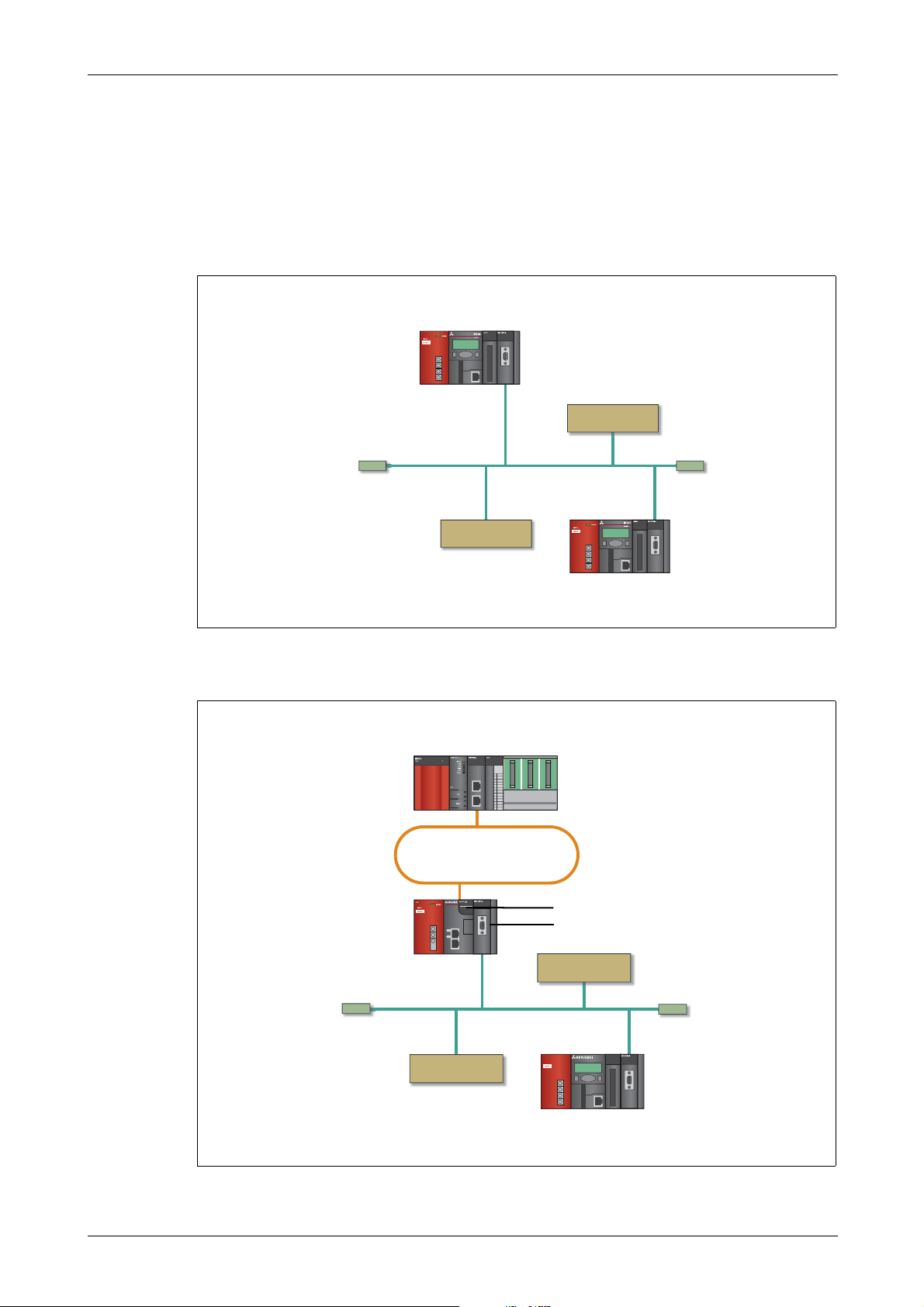
Overview System Configuration
Terminating
resistor
Terminating
resistor
CANopen Node
CANopen
Node
CANopen Node
(ME3CAN1-L)
CANopen Node
(ME3CAN1-L)
CAN bus network
Terminating
resistor
Terminating
resistor
CANopen Node
CANopen Node
CANopen Node
(ME3CAN1-L)
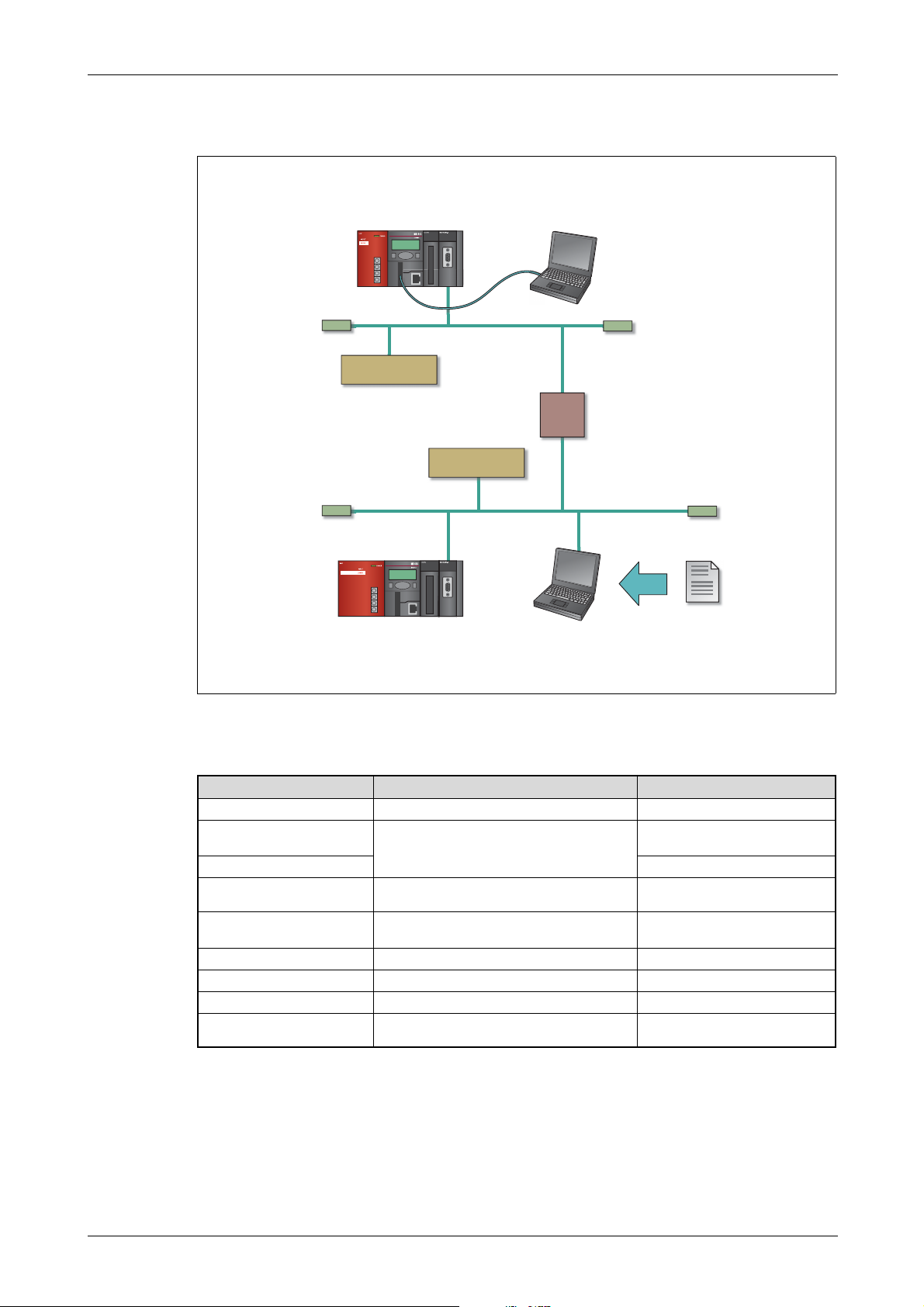
CC-Link IE Field Master/Local Module
(QJ71GF11-T2)
CC-Link IE Field
CANopen Module (ME3CAN1-L)
CC-Link IE Field Head module (LJ72GF15-T2)
CAN bus network
2 System Configuration
2.1 Overview
The ME3CAN1-L can be connected to a CPU module, an extension module or a CC-Link IE Field network head module of the MELSEC-L series.
Fig. 2-1:
L63P
MITSUBISHI
MITSUBISHI
L63P
ME3CAN1-L connected to a LCPU directly
MITSUBISHI
MELSEC-L Series – CANopen Module ME3CAN1-L 2 – 1
Fig. 2-2:
L02CPU
L02CPU
L02CPU
L02CPU
L02CPU
L02CPU
L02CPU
L02CPU
L02CPU
L02CPU
L02CPU
L02CPU
L02CPU
L02CPU
L02CPU
L02CPU
L63P
L63P
L63P
L63P
L63P
L63P
L63P
L63P
L63P
L63P
L63P
L63P
L63P
L63P
L63P
L63P
L63P
INPUT
INPUT
INPUT
INPUT
INPUT
INPUT
INPUT
INPUT
INPUT
INPUT
INPUT
INPUT
INPUT
INPUT
INPUT
INPUT
INPUT
24VDC
24VDC
24VDC
24VDC
24VDC
24VDC
24VDC
24VDC
24VDC
24VDC
24VDC
24VDC
24VDC
24VDC
24VDC
24VDC
24VDC
L02CPU
MITSUBISHI
MITSUBISHI
MITSUBISHI
MITSUBISHI
MITSUBISHI
MITSUBISHI
MITSUBISHI
MITSUBISHI
MITSUBISHI
MITSUBISHI
MITSUBISHI
MITSUBISHI
MITSUBISHI
MITSUBISHI
MITSUBISHI
MITSUBISHI
MITSUBISHI
POWER
POWER
POWER
POWER
POWER
POWER
POWER
POWER
POWER
POWER
POWER
POWER
POWER
POWER
POWER
POWER
POWER
L6DSPU
L6DSPU
L6DSPU
L6DSPU
L6DSPU
L6DSPU
L6DSPU
L6DSPU
L6DSPU
L6DSPU
L6DSPU
L6DSPU
L6DSPU
L6DSPU
L6DSPU
L6DSPU
L6DSPU
ME3CAN1-L connected to a CC-Link IE Field head module
Page 20

System Configuration Applicable Systems
C
Serial number
(first 5 digits)
Function
version
Model name
2.2 Applicable Systems
For the number of connectable modules and the compatible software version, refer to the following.
● MELSEC-L CPU Module User's M
● MELSEC-L CC
Restrictions when the ME3CAN1-L is connected to a head module
No special restriction is applied for the ME3CAN1-L.
-Link IE Field Network Head Module User's Manual
anual (Hardware Design, Maintenance and Inspection)
2.3 How to Check the Function Version and Serial No. of the Modules
The serial No. and function version can be checked on the label attached to the right side of the
module.
Using the programming software GX Works2, the serial No. and the function version can be checked
while the PLC is operating.
From the Diagnostics menu select System Monitor and then select Product Information List.
2 – 2
Fig. 2-3:
Product Information List for a PLC with a ME3CAN1-L
MITSUBISHI ELECTRI
Page 21
System Equipment System Configuration
Terminating
resistor
Terminating
resistor
CANopen Node
CANopen Node
MELSEC-L series PLC
with ME3CAN1-L
Configuration by FBs
in GX Works2
Repeater
USB cable
CAN bus network
Import
EDS file
Terminating
resistor
Terminating
resistor
CAN bus network
MELSEC-L series PLC
with ME3CAN1-L
3rd party
configuration tool
2.4 System Equipment
ME2PNR2-L
Fig. 2-4:
Product Description Note
ME3CAN1-L
Configuration tool integrated in
GX Works2
3rd party configuration tool —
D-sub connector
Terminating resistor
CAN bus network cable
CANopen node
Repeater
EDS file
Tab 2-1: System Equipment
Example for a system configuration with ME3CAN1-L
Module for CAN communication
Used to configure ME3CAN1-L (and CANopen
network)
Connector to connect ME3CAN1-L to the CAN
network
Resistor to terminate the CAN network. It is integrated in some D-sub connector.
Communication cable for CAN network
CANopen node from other manufacturer
Repeater for CAN network
Electronic data sheet (EDS) to describe the module. Used for 3rd party configuration tool.
—
—
—
Resistors are required to terminate
the CAN network at both ends.
—
—
—
—
MELSEC-L Series – CANopen Module ME3CAN1-L 2 – 3
Page 22

System Configuration System Equipment
C
2 – 4
MITSUBISHI ELECTRI
Page 23
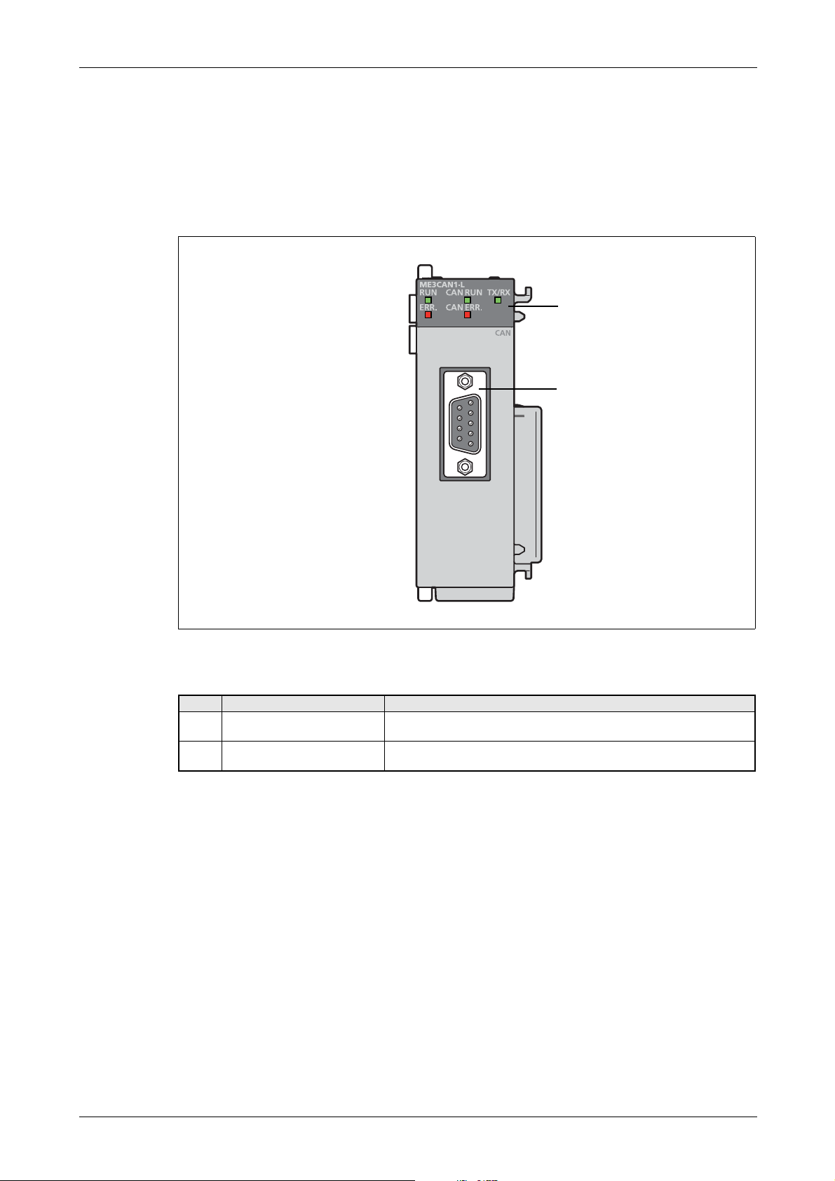
Part Names Detailed Description of the Module
3 Detailed Description of the Module
3.1 Part Names
This section explains the names of the components for the ME3CAN1-L.
Fig. 3-1: Names of parts
No. Name Description
ed to indicate the status of the ME3CAN1-L.
Indicator LEDs
CAN interface connector
(D-sub 9-pin male connec
tor)
Us
For a detailed description, please refer to section 3.1.1.
This connector connects the communication cable to the ME3CAN1-L.
For details, refer to section 3.1.2.
Tab. 3-1: Description of the LEDs and the connector of the ME3CAN1-L
MELSEC-L Series – CANopen Module ME3CAN1-L 3 – 1
Page 24

Detailed Description of the Module Part Names
3.1.1 Indicator LEDs
The LEDs are arranged in two groups:
● General LEDs are arranged on the left side.
● LEDs for CAN communication are arranged on the right side.
Fig. 3-2:
Indicator LEDs of the ME3CAN1-L
LED Color Status Description
RUN Green
ERR. Red
CAN RUN Green
CAN ERR Red
TX/RX Green
ON Normally operating
OFF Hardware error (watchdog timer error) or power failure
ON An module error has occurred.
OFF Normally operating
ON
FLICKERING* LSS services in progress.
BLINKING* CANopen쏐 mode: The device is in CANopen state Pre-operational.
SINGLE FLASH* The device is in CANopen쏐 state Stopped.
OFF Layer 2 mode: The device is in Layer 2 offline mode.
ON
FLICKERING* LSS Services in progress.
BLINKING* General error
DOUBLE FLASH*
SINGLE FLASH* Warning limit reached.
OFF No error
ON Module is transmitting/receiving CAN message
OFF Module is not transmitting/receiving CAN message
앫 CANopen쏐 mode: The device is in CANopen쏐 state Operational.
앫 Layer 2 mode: The device is in Layer 2 online mode.
앫 The CAN controller is Bus-OFF-state.
앫 The CAN controller has too many transmission errors.
Error control event
A NMT guarding failure (NMT-Slave or NMT-Master) or a heartbeat fail-
ure (heartbeat consumer) has occurred.
3 – 2
Tab. 3-2: Indicator LEDs
* The LEDs CAN RUN and CAN ERR have four kinds of flicker states (according to CiA쏐-303-3 V1.4): single flash, double flash,
blinking, and flickering. These LEDs flicker as follows.
SINGLE FLASH
0.2 s 1 s
DOUBLE FLASH
0.2 s 1 s0.2 s 0.2 s
BLINKING
0.2 s 0.2 s
FLICKERING
0.1 s
Page 25
Part Names Detailed Description of the Module
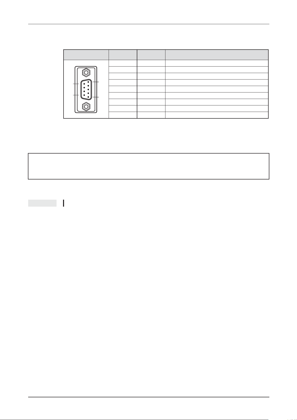
3.1.2 Signal Layout of the Connector
E
CANopen쏐 interface
connector
6
.
.
.
9
1
.
.
.
.
5
Pin no. Signal Description
1 — Reserved
2 CAN_L CAN_L bus line (dominant low)
3 CAN_GND CAN ground
4 — Reserved
5 CAN_SHLD CAN shield
6 — Reserved
7 CAN_H CAN_H Bus line (dominant high)
8 — Reserved
9 — Reserved
Tab. 3-3: Pin assignments of the CAN interface connector (D-sub 9-pin male connector) on the
ME3CAN1-L
WARNING:
Leave the "reserved" pins unconnected.
NOTE An inch screw thread (#4-40UNC) is used to fix the connector to the ME3CAN1-L.
For the wiring of the CANopen쏐 module ME3CAN1-L please refer to section 6.3.2.
MELSEC-L Series – CANopen쏐 Module ME3CAN1-L 3 – 3
Page 26

Detailed Description of the Module Specifications
C
3.2 Specifications
The specifications for the ME3CAN1-L are shown in the following table. For general specifications,
refer to the operation manual for the CPU module being used.
Specification ME3CAN1-L
Transmission type CAN Bus network (RS-485, CSMA/CR)
Applicable functions
CANopen communication services according
to CiA standards
CANopen device and application profiles
according to CiA Standards
Remote Transmit Request (RTR)
Node number Selectable from 1 to 127
Communication method Acyclic, cyclic or event-driven
Supported transmission speed / maximum
bus length
Connection cable
Connection to CANopen network via 9-pin D-sub connector
Insulation method
Number of occupied I/O points 32 points (I/O assignment: Intelligent 32 points)
Internal current consumption (5 V DC) 0.39 A
Weight 0.14 kg
앫 CANopen Node
앫 CAN Layer 2 Node
앫 CiA-301 V4.2
앫 CiA-302 V4.1
앫 CiA-305 V2.2
Interface and Device Profile CiA-405 V2.0 for IEC 61131-3 Programmable
Devices
앫 Layer 2 mode: supported
앫 CANopen mode: not supported for PDO
The maximum bus length varies depending on the transmission speed.
앫 1 Mbps / 25 m
앫 800 kbps / 50 m
앫 500 kbps / 100 m
앫 250 kbps / 250 m
앫 125 kbps / 500 m
앫 100 kbps / 600 m
앫 50 kbps / 1,000 m
앫 20 kbps / 2,500 m
앫 10 kbps / 5,000 m
The cable should conform to ISO11898.
Recommended is a shielded 2x2 twisted pair cable with an impedance of
about 120 (refer to section 6.3.2).
앫 Photocouplers are used to insulate the CAN input from the PLC.
앫 A DC/DC converter is used to insulate the power supply from the CAN
input.
3 – 4
Tab. 3-4: Specifications of the ME3CAN1-L
MITSUBISHI ELECTRI
Page 27
Specifications Detailed Description of the Module
4
DIN rail center
45
Unit: mm
(45)
95
90
4
4
28.5
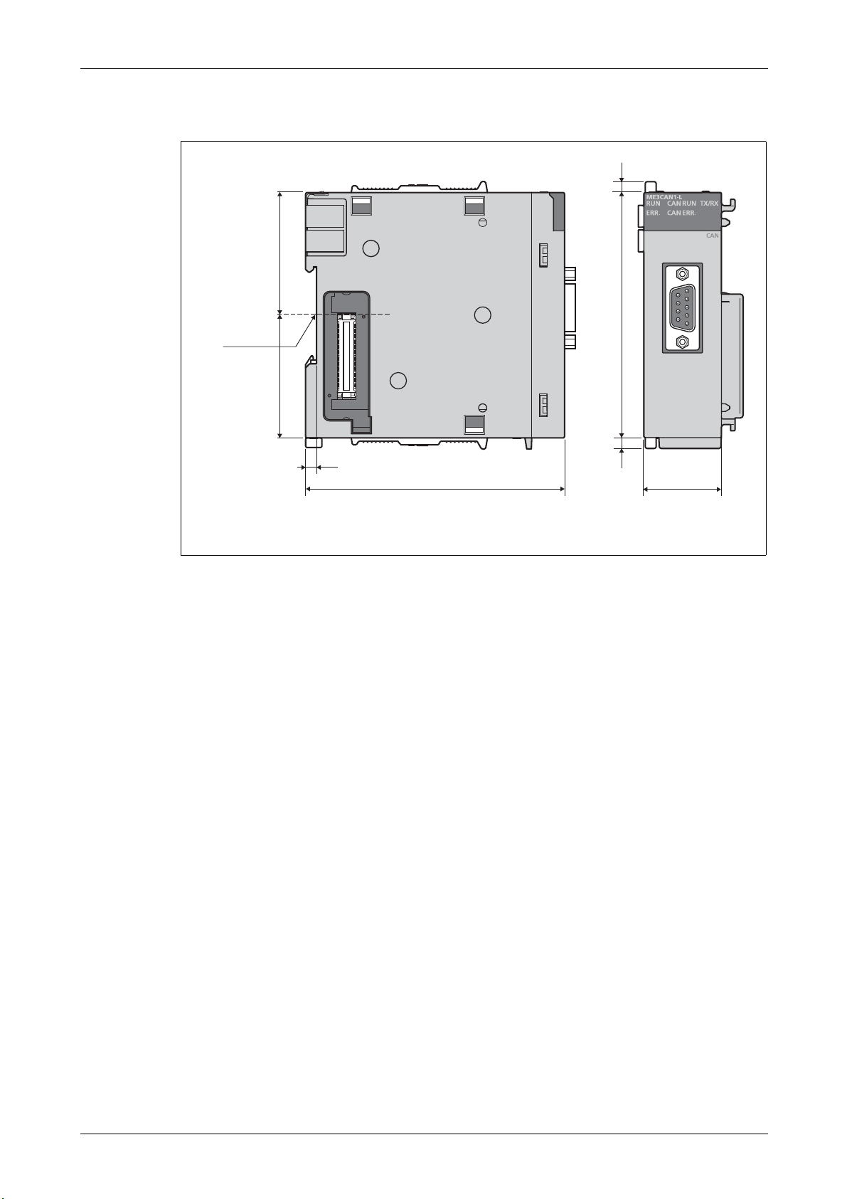
3.2.1 External Dimensions
Fig. 3-3: Dimensions of the ME3CAN1-L
MELSEC-L Series – CANopen Module ME3CAN1-L 3 – 5
Page 28

Detailed Description of the Module I/O Signals for the Programmable Controller CPU
C
3.3 I/O Signals for the Programmable Controller CPU
3.3.1 List of I/O signals
Note that the I/O numbers (X/Y) shown in this section and thereafter depend on the mounting position resp. on the start I/O number or head address of the ME3CAN1-L. This head address has to be
added to the shown I/O numbers.
For example, if the ME3CAN1-L occupies the range from X/Y040 to X/Y05F the head address is X/Y040.
However the least significant digit is omitted and the head address "n" in this case reads as "4". The "module ready" input (Xn0) will be X40 and the "EMCY message available" signal (X(n+1)1) will be X51.
Signal direction CPU Module ME3CAN1-L Signal direction CPU Module ME3CAN1-L
Device No. (Input) Signal name Device No. (Output) Signal name
Xn0 Module ready Yn0 Use prohibited
Xn1 Data exchange completed Yn1 Data exchange request
Xn2 Module restart completed Yn2 Module restart
Xn3
Xn4
Xn5
Xn6 Yn6
Xn7 Yn7
Xn8 Yn8
Xn9 Yn9
XnA YnA
XnB YnB
XnC YnC
XnD YnD
XnE YnE
XnF ME3CAN1-L error YnF ME3CAN1-L error clear request
X(n+1)0
X(n+1)1
X(n+1)2
X(n+1)3
X(n+1)4
X(n+1)6 Y(n+1)6
X(n+1)7 Command execution completed Y(n+1)7 Command execution request
X(n+1)8
X(n+1)9 Y(n+1)9
X(n+1)A Y(n+1)A
X(n+1)B Y(n+1)B
X(n+1)C Y(n+1)C
X(n+1)D Y(n+1)D
X(n+1)E Y(n+1)E
X(n+1)F
Module in Layer 2 online mode
(Layer 2 modes only)
Message transmit trigger completed
(Layer 2 modes only)
Use prohibited
NMT Error Control failure available
(CANopen mode only)
EMCY message available
(CANopen mode only)
Time stamp setting completed
(CANopen mode only)
Time stamp information is available in
buffer memory (CANopen mode
only)
Use prohibited
Use prohibited
Save configuration / restore factory
default completed
Yn3
Yn4
Yn5
Y(n+1)0
Y(n+1)1
Y(n+1)2
Y(n+1)3
Y(n+1)4
Y(n+1)8
Y(n+1)F
Layer 2 online mode request
(Layer 2 modes only)
Message transmit trigger request
(Layer 2 modes only)
Use prohibited
NMT Error Control failure clear
request (CANopen mode only)
EMCY message area clear request
(CANopen mode only)
Time stamp set request
(CANopen mode only)
Time stamp read request
(CANopen mode only)
Use prohibitedX(n+1)5 Y(n+1)5
Use prohibited
Save configuration / restore factory
default configuration request
Tab. 3-5: I/O signals of the ME3CAN1-L
NOTE The "Use prohibited" signals cannot be used by the user since they are for system use only.
If these are turned ON/OFF by the sequence program, the performance of the CANopen module
cannot be guaranteed.
3 – 6
MITSUBISHI ELECTRI
Page 29

I/O Signals for the Programmable Controller CPU Detailed Description of the Module
3.3.2 Details of I/O signals
Module ready signal (Xn0)
● This signal turns ON when the ME3CAN1-L is enabled for access from the CPU module.
● This signal turns OFF when the ME3CAN1-L is disabled for ac
module watchdog timer error or hardware fault.
Data exchange completed (Xn1), Data exchange request (Yn1)
● These signals are used to exchange data between the buffer memory of the ME3CAN1-L and the
CA
Nopen object dictionary/Layer 2 message buffer.
● To ensure that the ME3CAN1-L can handle the C
to set the data exchange request (Yn1) to ON after writing the data. The Data exchange completed
(Xn1) and Data exchange request (Yn1) signals control the internal buffer exchange and thereby
which data is transmitted from the PLC by PDO.
● PDO transmit data will only be sent to the CAN bus if the module is in NMT state Operational and
af
ter setting Yn1 to ON. As long as the reading of the previous data is not finished and a new data
exchange command has not been sent, data will not be overwritten by further PDO.
If the module is in NMT state Operational, the received PDO data from other nodes can be read
by the MELSEC-L series CPU by using a FROM instruction and the transmit PDO data can be written
to the module and sent to the network by using
signal (Xn1) will be turned ON when the data exchange between buffer memory and Object
Dictionary/Data exchange buffer is finished.
● Depending on the bits turned ON in the Data Exchange Control (Un\G20), OD data and/or EMCY
data will be ex
NOTE If Xn1 is turned ON and the module is not in CANopen state Pre-operational or Stopped, the PDO
data will be exchanged after going into Operational state.
changed.
ANopen data in a consistent way, it is necessary
a TO instruction. The data exchange completed
cess from the CPU module due to a
MELSEC-L Series – CANopen Module ME3CAN1-L 3 – 7
Page 30
Detailed Description of the Module I/O Signals for the Programmable Controller CPU
C
Performed by the ME3CAN1-L
Performed by the sequence program
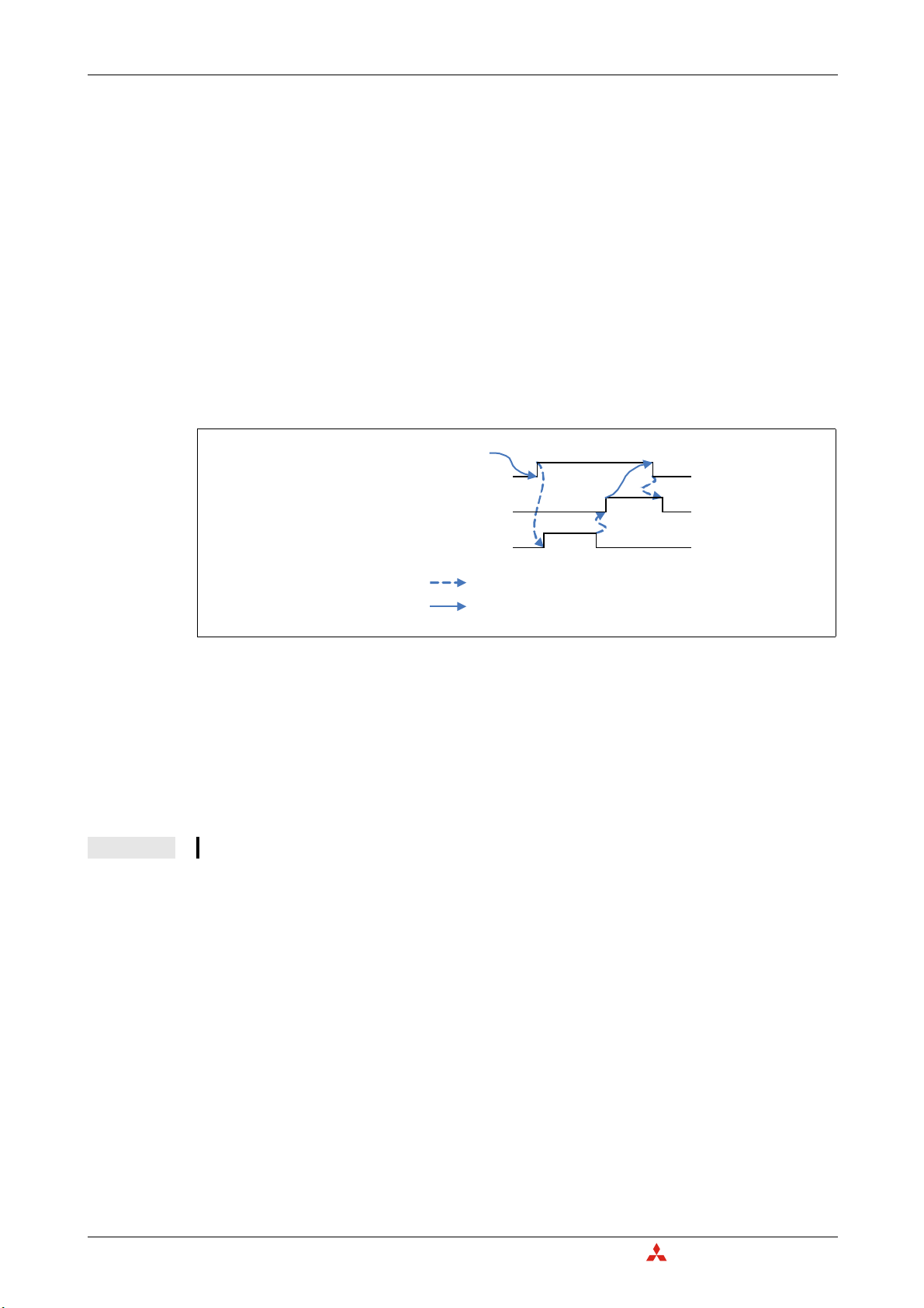
Module restart request (Yn2)
Module restart completed (Xn2)
Module initialization state (Un\G25 bit 7)
OFF
OFF
ON
ON
OFF
ON
Module restart completed (Xn2), Module restart request (Yn2)
● A restart is necessary to activate the following new settings:
– Function mode (Un\G21), refer to section 3.5.2
– Baud rate (Un\G24), refer to section 3.5.4
– Node-ID (Un\G27), refer to section 3.5.6
– NMT master setting, refer to section 4.8.5.
All not saved settings will be lost.
● To restar
t the module
, please set the module restart request (Yn2) signal to ON. The module will
be set to initialization state as indicated by the Un\G25 bit 7 (refer to section 3.5.5). After the
module is restarted, the module restart completed (X
n2) will be set to ON. The module restart
request (Yn2) signal can be reset to OFF. Not setting this signal back to OFF will cause that the
module will be restarted again and again. The restart procedure will take approx. 6 seconds to
complete.
Fig. 3-4: Timing of the signals Xn2 and Yn2
Module in Layer 2 online mode (Xn3), L
● The Layer 2 online mode request signal (Yn3) must be set to ON to star
yer 2 online mode request (Yn3)
a
t data exchange with other
network nodes.
● The module in Layer 2 online mode signal (X
mode. The configuration of the module can only be changed while this signal is OFF..
NOTE In case a configuration buffer memory was changed during online mode, Un\G29 bit 5 is set to ON.
Message transmit trigger completed (Xn4), Message transmit trigger request (
● The transmission trigger of a message in Layer 2 mode which is set in Un\G8400 to Un\G8402
must be star
● The message transmit trigger completed signal (X
been written into the transmit buffer. Please refer also to section 3.6.4.
3 – 8
n3) will turn ON if the module can be set to online
ted with a message transmit trigger request (Yn4).
Yn4)
n4) will turn ON when all the messages have
MITSUBISHI ELECTRI
Page 31

I/O Signals for the Programmable Controller CPU Detailed Description of the Module
Performed by the ME3CAN1-L
Performed by the sequence program
Error (Un\G29)
ME3CAN1-L error (XnF)
ME3CAN1-L error clear request (YnF)
OFF
OFF
ON
ON
ON
OFF
ME3CAN1-L error (XnF), ME3CAN1-L error clear request (YnF)
● If one or more of the following bits in the buffer memory address Un\G29 (error state) are turned
ON, XnF will be turned ON: Bits 1, 2, 4, 5, 6, 8, or 15. Please refer to section 3.5.7.
● If XnF is turned ON, if necessary please take correct
ive action to remove the error cause and then
turn ON YnF to clear the error signals XnF and the bits in the error state (Un\G29).
● If a new error is generated while the ME3CAN1-L error clear request (
YnF) is ON, this will be cleared
automatically.
● After the ME3CAN1-L error clear request (YnF) is turned OFF
, the ME3CAN1-L will check for new
errors again.
Fig. 3-5: Timing of the signals XnF and YnF
NMT Error Control failure available (X(n+1)0), NMT Error Control failure clear request (Y(n+1)0)
● If there is at least one CANopen
NMT Error Control failure (at least one of the assigned NMT slaves
failed during NMT Error Control), the NMT error of CANopen node available (X(n+1)0) will turn
ON.
● How to clear the error of all nodes
H
To clear the error of all nodes, write 0000
to Un\G400 (this is the default setting of Un\G400) and
turn ON the Clear NMT Error Control failure request (Y(n+1)0). The NMT error control failures of
all nodes will be then cleared and the NMT Error Control failure available (X(n+1)0) will be turned
OFF.
● How to clear the error of a certain node
To clear the error of a node
failure clear request (
, write the node number to Un\G400 and turn ON NMT Error Control
Y(n+1)0). The NMT error control failures of this node will be cleared and if
there no other NMT error control failures the NMT Error Control failure available (X(n+1)0) will also
be turned OFF.
● If a new error is genera
ted while the NMT Error Control failure clear request (Y(n+1)0) is ON, this
will be cleared automatically.
● After the NMT Error Control failure Clear request (
Y(n+1)0) is turned OFF, the ME3CAN1-L will
check for new errors again.
● For more error details on NMT Error Control failure
, please refer to section 3.5.15.
MELSEC-L Series – CANopen Module ME3CAN1-L 3 – 9
Page 32

Detailed Description of the Module I/O Signals for the Programmable Controller CPU
C
Performed by the ME3CAN1-L
Performed by the sequence program
EMCY message available (X(n+1)1)
EMCY message area clear request (Y(n+1)1)
EMCY messages
OFF
OFF
ON
ON
No EMCY data
EMCY
data
available
No EMCY data (cleared)
EMCY message available (X(n+1)1), EMCY message area clear request (Y(n+1)1)
● If there is at least one CANopen emergency received (reception of an Emergency message from
at least one activated EMCY consumer objects), the EMCY message available (X(n+1)1) will turn
ON.
● To clear all EMCY messages,
turn ON the EMCY message area clear request (Y(n+1)1). All EMCY
messages will be then cleared and the EMCY message available (X(n+1)1) will be turned OFF.
● If a new EMCY message is received while the EMCY message area clear request (Y(n+1)1) is ON,
this will be cleared automatically.
● After the EMCY message area clear request (Y(n+1)1) is turned OFF
, the ME3CAN1-L will store the
newly received EMCY messages again.
For more error details, please refer to the sections 4.6.12 and 3.5.17.
Fi
g. 3-6: Ti
ming of the signals X(n+1)1 and Y(n+1)1
Time stamp setting completed (X(n+1)2), Time stamp set request (Y(n+1)2)
After setting the necessary time stamp information in Un\G50 to Un\G58, please turn ON the time
stamp set request (
A
fter the setting is finished, the time stamp setting completed signal (X(n+1)2) will be turned ON, and
Y(n+1)2).
the request signal can be turned OFF. When the ME3CAN1-L is the current network master and Producer, then the first time stamp will be sent.
Time stamp information is available in buffer memory (X(n+1)3), Time stamp read request
(
(n+1)3)
Y
To read the time stamp, please set the time stamp read request (Y(n+1)3) to ON.
The time stamp information will be stored in the buffer memory addresses Un\G50 to Un\G58 and the
time stamp information is available in buffer memory
(X(n+1)3) signal will be turned ON to indicate
that actual time stamp information is available.
Command 1 execution completed (X(n+1)7, Command 1 e
ecution request (Y(n+1)7)
x
● These signals are used for execution of Command Interface 1.
● After writing the necessary command par
ameter (refer to section 3.5.18), turn ON Y(n+1)7 to
execute the command. If the command execution is finished, X(n+1)7 will be turned ON.
3 – 10
MITSUBISHI ELECTRI
Page 33

I/O Signals for the Programmable Controller CPU Detailed Description of the Module
Save configuration/Restore factory default completed (X(n+1)F), Save configuration/Restore
factory default configuration request (Y(n+1)F)
These signals are used to execute the save configuration / restore factory default request. The request
must be specified in Un\G22 (Save/Restore Configuration, refer to sec
tion 3.5.3). After that the request
can be executed by setting Y(n+1)F to ON. When the request is completed, the corresponding bits in
Un\G22 will be cleared, and X(n+1)F will be turned ON.
NOTE
앫
If both bits Un\G22.0 and Un\G22.1 are set simultaneously the buffer memory and Flash ROM will
be reset to factory defaults.
앫
If only bit Un\G22.1 is set, factory default values are written to the configuration buffer memory
but not stored in Flash ROM. In order to store changes made to the configuration execute the
Save configuration request (Un\G22.0 then Y(n+1)F) after changing the configuration.
MELSEC-L Series – CANopen Module ME3CAN1-L 3 – 11
Page 34

Detailed Description of the Module Buffer Memory Overview
C
Bit
Buffer memory address
3.4 Buffer Memory Overview
The CANopen module has a memory range assigned as a buffer for temporary storage of data, such
as Received Process Data or CAN transmission error counter. The PLC CPU can access this buffer and
both read the stored values from it and write new values to it which the module can then process
(Transmit Process Data etc.).
Each buffer memory address consists of 16 bits.
Fig. 3-7: Assignments of bits to a buffer memory address
NOTE Do not write data in the "system areas" of the buffer memory. If data is written to any of the system
areas, the PLC system may not be operated properly. Some of the user areas contain partially system areas. Care must be taken when reading/writing to the buffer memory.
Also, do not write data (e.g. in a sequence program) to the buffer memory area where writing is
disabled. Doing so may cause malfunction.
The "Default" value indicated in the following tables is the initial value set af
or the PL
Instructions for data exchange with the buffer memory
Communication between the PLC CPU and the buffer memory of special function modules is per
formed with FROM and TO instructions.
The buffer memory of a special function module can also be accessed directly, e. g. with a MOV
instruction. The special function module addressed in this way can be mounted on a base unit or an
extension base unit but not in remote I/O stations.
Format of the device address: Un\Gn
– Un: Head address of the special function module
– Gn: Buffer memory address (decimal)
For example the device address U3\G11designates the buffer memory address 11 in the special function module with the head address 3 (X
In this User's Manual the latter form of addressing is used throughout.
For full documentation of all the instructions with examples please refer to the Programming Manual
for the MELSEC System Q and the L series.
C CPU is reset.
/Y30 to X/Y3F).
ter the power is turned on
-
NOTE As long as Un\G25 bit 7 is ON ("Module is in initialization state"), any write access to the buffer
3 – 12
memory is prohibited and will generate a Un\G29 bit 5 error. Refer to section 3.5.7.
MITSUBISHI ELECTRI
Page 35

Buffer Memory Overview Detailed Description of the Module
3.4.1 Buffer Memory Assignment
Address
(Decimal)
Description Default R/W
Stored to
Flash ROM
Reference
(Section)
0–19 System area — — — —
20 Data Exchange Control 0
H
R/W — 3.5.1
21 Function mode 405 R/W ✔ 3.5.2
22 Save/Restore Configuration 0
H
R/W — 3.5.3
23 System area — — — —
24 Baud Rate 250 R/W ✔ 3.5.4
25 Communication Status 80
H
R/W — 3.5.5
26 System area — — — —
27
Node Address
(CANopen modes only)
127 R/W ✔ 3.5.6
28 System area — — — —
29 Error Status 0
H
R/W — 3.5.7
30–34 System area — — — —
35 CAN transmission error counter 0
36 CAN reception error counter 0
H
H
R — 3.5.8
R — 3.5.9
Baud Rate display
37
Diagnose display for the current baud rate of the CAN
2500 R — —
Controller in multiples of 0.1kbps.
Sampling Point display
38
Diagnose Display for the current sampling point of
875 R — —
the CAN Controller in multiples of 0.1%.
39 Buffer memory setting error display 0
40
Buffer memory initialization/online mode write error
display
H
0
H
R—
R—
3.5.10
41–49 System area — — — —
50
Producer/consumer 1
51 Year 14
52 Month 8
53 Day 1
54 Hour 0
55 Minute 0
Time stamp
(CANopen modes
only)
R/W
—
3.5.11
56 Second 0
57 Day-of-the-week 5R
58 Transmission interval
0R/W
59 Daily correction (CANopen modes only) 0 R/W ✔
60–69 System area — — — —
70
71
NMT Start all Nodes delay
(CANopen modes only)
SDO Time out
(CANopen modes only)
500 R/W ✔ 3.5.12
500 R/W ✔ 3.5.13
72–399 System area — — —
400 NMT error clear node 0
401–527
NMT Error Control Status
(CANopen modes only)
H
0
H
R/W — 3.5.14
R/W — 3.5.15
528–600 System area — — — —
601–726
727 7F
NMT State
(CANopen modes only)
728–749 System area 0
750–859
EMCY Message Buffer
(CANopen modes only)
0
H
H
H
0
H
R — 3.5.16
— — —
— — 3.5.17
860–999 System area — — — —
1000–1066 Command Interface 0
H
R/W — 3.5.18
1067–5000 System area — — — —
5001–5042
Message Slot error code list
(Layer 2 function modes only)
0
H
R/W — 3.6.1
Tab. 3-6: Buffer memory assignment of the ME3CAN1-L
MELSEC-L Series – CANopen Module ME3CAN1-L 3 – 13
Page 36

Detailed Description of the Module Buffer Memory Overview
C
Address
(Decimal)
Description Default R/W
Stored to
Flash ROM
Reference
(Section)
5043–5999 System area — — — —
6000–8167
Pre-defined Layer 2 message configuration
(Layer 2 modes only)
—R/W ✔ 3.6.2
8168–8349 System area — — — —
8350–8352
Layer 2 RTR flags
(Layer 2 modes only)
0
H
R — 3.6.3
8353–8399 System area — — — —
8400–8402
Message transmit trigger flags
(Layer 2 modes only)
0
H
R/W — 3.6.4
8403–8449 System area — — — —
8450–8477
PLC RUN>STOP messages
(Layer 2 modes only)
0
H
R/W ✔ 3.6.5
8478–9999 System area — — — —
Layer 2 modes only
10000–10293 Receive / Transmit Process Data 0
H
R/W — 3.6.6
From 10294 System area — — — —
405 Mode only
10000–11023 Receive Process Data (RPDO) 0
H
R — 3.5.19
11024–12999 System area — — — —
13000–15047 Transmit Process Data (TPDO) 0
H
R/W — 3.5.19
From 15048 System area — — — —
Tab. 3-6: Buffer memory assignment of the ME3CAN1-L
Indicates whether reading from and writing to a sequence program are enabled.
R: Read enabled
W: Write enabled
Only in Layer 2 mode the contents of some buffer memory addresses is stored into the Flash-ROM (Refer to section 3.6.6).
3 – 14
MITSUBISHI ELECTRI
Page 37

Buffer Memory Details: CANopen Mode Detailed Description of the Module
3.5 Buffer Memory Details: CANopen Mode
3.5.1 Data Exchange Control (Un\G20)
This buffer memory address allows the control of the OD and EMCY data exchange.
Bit Description
0–7 Reserved
Only in CANopen modes: Data exchange mode setting (only OD data)
Bit = 0: No data exchange between buffer memory and CANopen object dictionary
Bit = 1: Activate data exchange between buffer memory and CANopen object dictionary
8
NOTES:
앫 The data will be also exchanged if this entire buffer memory address is set to 0 (default value).
앫 If the bit is set and the module is not in CANopen state Operational, the PDO data will be exchanged after
going into Operational state.
9–11 Reserved
Data exchange status (only EMCY data)
Bit = 0: No data exchange between Emergency Message buffer memories and EMCY Receive Buffer
Bit = 1: Exchange data between Emergency Message buffer memories and EMCY Receive Buffer
12
For more information please refer to section 3.5.17
NOTE:
앫 The data will be also exchanged if this entire buffer memory address is set to 0 (default value).
13–15 Reserved
Tab. 3-7: Assignment of the bits in buffer memory address Un\G20
3.5.2 Function Mode (Un\G21)
The ME3CAN1-L chooses the communication function corresponding to the function mode set in the
buffer memory address 21.The possible settings are shown in the following table:
Set value Function Mode Description
11 11 bit CAN-ID Layer 2 mode This mode supports the 11 bit CAN-ID Layer 2 Message.
29 29 bit CAN-ID Layer 2 mode This mode supports the 29 bit CAN-ID Layer 2 Message.
405 CANopen 405 mode
Other value —
Tab. 3-8: Function mode setting in buffer memory address Un\G21
The buffer memory setting needs to be stored by Un\G22 bit 0 and afterwards to be restar
to make the new settings effective (Refer to section 3.5.3 and section 3.3.2).
NOTE During a restart, all Object Dictionary (OD) settings will be deleted when the CANopen mode is
changed.
This mode supports the CANopen CiA 405 IEC 61131-3 Programmable Device Profile.
All other settings will generate an error (in this case bit 6 in Un\G29 is
set (Refer to section 3.5.7).
ted by Yn2
MELSEC-L Series – CANopen Module ME3CAN1-L 3 – 15
Page 38

Detailed Description of the Module Buffer Memory Details: CANopen Mode
C
3.5.3 Save/Restore Configuration (Un\G22)
This buffer memory specifies two bits that allow to restore the factory default configuration in the buffer memory and to store the buffer memory configuration into the Flash ROM. To execute the request,
please set Y(n+1)F to ON (refer to section 3.3.2).
Both bits will be reset automatically if the restore or save procedure is completed, and X(n+1)F will
turn ON.
Bit Description
0 Bit = 1:Save configuration to Flash ROM
1
Bit = 1: Restore factory default configuration (not saved to Flash ROM)
2–15 Reserved
Tab. 3-9: Assignment of the bits in buffer memory address Un\G22
NOTES
If both bit 0 and bit 1 are set simultaneously the buffer memory and Flash ROM will be reset to the
factory defaults.
If only bit 1 is set, factory default values are written to the configuration buffer memory but not
stored in the Flash ROM. In order to store changes made to the configuration buffer memory, set
Un\G22 bit 0 after changing the configuration.
3.5.4 Baud Rate (Un\G24)
In Un\G24 the baud rate is set. The current baud rate can be found in Un\G37.
Value in Un\G24 Baudrate
10
20
50
100
125
250
500
800
1000
10 kbps
20 kbps
50 kbps
100 kbps
125 kbps
250 kbps
500 kbps
800 kbps
1000 kbps
Tab. 3-10:
Settings for the baud rate
NOTES The baud rate must be equal for all nodes in the network.
The new value needs to be stored by Un\G22. Then Y(n+1)F has to be turned ON and the module
has to be restarted to make the new setting effective.
At low baud rates a too fast data exchange and/or high bus load can result in a transmission data
queue overflow error (bit 8 in Un\G29, refer to section 3.5.7).
3 – 16
MITSUBISHI ELECTRI
Page 39

Buffer Memory Details: CANopen Mode Detailed Description of the Module
3.5.5 Communication Status (Un\G25)
The buffer memory address Un\G25 displays the ME3CAN1-L communication status.
Bit Description
CANopen modes:
0
Bit = 0: Not in Operational State
Bit = 1: Operational State
Bit = 0: The error counter is below the warning level. (Refer to sections 3.5.8 and 3.5.9)
1
Bit = 1: The error counter of the CAN controller has reached the warning level.
2
3
Reserved
4
5
Bit = 0: No NMT Reset received.
Bit = 1: The CANopen Application was reset by an NMT Reset communication or NMT Reset Application com-
6
7
8
9
10
11 Reserved
12
13 Reserved
14
15
mand. All unsaved changes in the Object dictionary are lost and are set to factory default or to the former
stored value.
Write a 0 to reset the bit. (Refer to sections 4.8.8 and 4.6.10). The bit is set to 0 in the beginning of the reset process.
Module initialization state
Bit = 0: Module initialization finished
Bit = 1: Module is in initialization state
The module is initializing the internal data structures and the buffer memory.
While this bit is on, it is recommended to execute a read access to Un\G25 and Un\G29 only.
In case of a module restart request with Yn2 or over a CANopen NMT command this bit will be set.
This bit shall be monitored in the PLC program all the time to prohibit Un\G29 failures.
CANopen Network state
Bit 9 Bit 8 Description
00Stopped State
01Pre-operational State
10Operational State
11Reserved
Bit = 0: LSS Master routine inactive
Bit = 1: LSS Master routine active
This bit is only "1" when the LSS Master is searching and configuring LSS Slaves.
Bit = 0: No Time Stamp object received or bit is reset
Bit = 1: Time Stamp object received (Only if Consumer is set)
Write a 0 to reset the bit. (Refer to sections 4.6.9 and 3.5.11)
Bit = 0: NMT Start-up Master:
No Slave start-up in progress
Bit = 1: NMT Start-up Master: Slave start-up in progress (Refer to section 4.8.5)
Note:
This bit goes on during the NMT master/slave startup and any time when a NMT slave error occurs and the NMT
startup master tries to re-start the faulty NMT slave.
Bit = 0: Module works as NMT Slave
Bit = 1: Module works as NMT Master
Tab. 3-11: Assignment of the bits in buffer memory address Un\G25
3.5.6 Node Address (Un\G27)
The buffer memory address 27 sets the CANopen Node-ID. The setting value range is 1 to 127.
The buffer memory setting needs to be stored by Un\G22 bit 0 and afterwards to be restarted by Yn2
to make the new setting effective (Refer to section 3.5.3).
A setting out of the above range or a write access in Layer-2 function mode will generate a failure message in Un\G29 bit 6.
MELSEC-L Series – CANopen Module ME3CAN1-L 3 – 17
Page 40

Detailed Description of the Module Buffer Memory Details: CANopen Mode
C
3.5.7 Error state (Un\G29)
The following table shows the description of the error if a bit in the buffer memory address Un\G29 is
set.
Bit Error Description/Corrective action
0 Reserved
1 Hardware error
2 Reserved
3 The CAN controller is bus OFF.
4 FLASH memory error
Invalid write access in Layer 2
5
mode
6 Buffer memory setting error
7 Reserved
8 Internal data queue overflow
9
10
Reserved
11
12
13
14 CAN error passive state
Layer 2 Message Slot specific
15
error exists.
This bit can only be reset by switching the power OFF/ON.
Contact your Mitsubishi Electric representative.
The CAN controller has too many transmission errors (Refer to section 3.5.8).
Restart the Module (Refer to section 3.3.2).
Invalid data in the Flash memory might be caused by power loss during a write
operation to the Flash ROM.
If this bit is not cleared after a module restart (Yn2) or another power cycle, please
contact your Mitsubishi Electric representative.
Invalid write access to configuration buffer memory while in ONLINE/INIT mode.
Check user program, do not write into configuration buffer memory when mod-
ule is ONLINE.
In Un\G40 the buffer memory address where this failure occurred will be
displayed.
This bit is set if an attempt to write an invalid value into a buffer memory is
detected.
The target buffer memory address of the invalid write access is displayed in
Un\G39 (Refer to section 3.5.10). Check Un\G39 for buffer memory address and
correct set value to valid range.
Extreme bus load can cause the internal queues to overflow.
Decrease the bus load. At a low baud rate a too fast data exchange (refer to section 3.5.1) can overflow the CAN Transmit Buffer (Depends also on the bus-load of
the CAN).
This bit shows the CAN error active state/passive state.
Bit = 0: Error active state
Bit = 1: Error passive state
This bit will be reset automatically if the internal error counters return back below
128. (Refer to sections 3.5.8 and 3.5.9)
Check the Message Slot specific error code in Un\G5001–Un\G5584 (Refer to section 3.6.1).
3 – 18
Tab. 3-12: Assignment of the bits in buffer memory address Un\G29
Layer 2 modes: The configuration must not be changed when the module is set to ONLINE, before changing the configuration set Yn0 to OFF (configuration mode) and wait until Xn0 is OFF (module OFFLINE/INIT). The affec
buffer memories are Un\G10000 to Un\G10293, Un\G6000 to Un\G6167 and Un\G8400 to Un\G8402.
Any CANopen node will check all CAN messages on the bus for errors. Depending on the error state the action that the
node will take is different:
앫 In error ac
The node will ac
앫 In error passive state:
The node will not actively mark the frame as invalid to avoid bus disturbance if the node itself has an H/W problem.
tive state:
tively mark the frame as invalid.
ted configurations
If one or more of the bits 1, 4, 6, 8, or 15 in UN\G29 are set, XnF will be turned ON.
The bits 5 6, 8, and 15 are latched and it is necessary to set YnF to ON which will clear all latched error
bits in Un\G29. All other bits are reset automatically if the cause for the error is solved.
MITSUBISHI ELECTRI
Page 41

Buffer Memory Details: CANopen Mode Detailed Description of the Module
3.5.8 CAN transmission error counter (Un\G35)
The ME3CAN1-L stores the current value of the CAN transmit error counter. The displayed value range
is 0 to 256.
The counter counts 8 up if a transmission error is detected. For each transmission without error, the
counter counts 1 down.
Value in Un\G35 Description
0 to 127 Error active state
96 to 127 Warning level
128 to 255 Error passive state
256 Bus OFF state
NOTE
The warning level is also shown by bit 1 in Un\G25, error passive and Bus OFF are shown in
Un\G29.
3.5.9 CAN reception error counter (Un\G36)
The ME3CAN1-L stores the current value of the CAN reception error counter. The displayed value
range is 0 to 128 and 256.
The counter counts 8 up if a reception error is detected. For each reception without error, the counter
counts 1 down.
Value in Un\G36 Description
0 to 127 Error active state
96 to 127 Warning level
128 Error passive state
256 Bus OFF state
Tab. 3-13:
Meaning of the values for the transmission error
counter
Tab. 3-14:
Meaning of the values for the reception error
counter
NOTE
The warning level is also shown by bit 1 in Un\G25, error passive and Bus OFF are shown in
Un\G29.
3.5.10 Buffer memory setting error display (Un\G39, Un\G40)
Buffer memory setting error display (Un\G39)
Bit 6 of Un\G29 is set to ON if an attempt to write an invalid value into a buffer memory address is
ed. The content of Un\G39 shows the buffer memory address where this failure occurred. In
detect
case of a multiple write error, the first failure will be displayed. The buffer memory will be reset by setting YnF to ON.
Buffer memory initialization / online mode write error display (Un\G40)
If a write access is done while the module is in Layer 2 online mode or in initialization mode, bit 5 of
Un\G29 is set to "1" and Un\G40 indicates the buffer memory address, where this failure has occurred.
In case of a multiple write error, the first failure will be displayed. The buffer memory will be reset by
setting YnF to ON.
MELSEC-L Series – CANopen Module ME3CAN1-L 3 – 19
Page 42

Detailed Description of the Module Buffer Memory Details: CANopen Mode
C
3.5.11 Time stamp (Un\G50–Un\G59)
CANopen devices which operate a local clock may use the TIME object to adjust their own time base
to the time of the time stamp producer.
After each power up or restart the date and time are set to the default values and the counting is
stopped.
If the ME3CAN1-L is set to "consumer", the clock starts counting after receiving the first time stamp
object.
When the module is setup as "producer", the counter starts after setup of Un\G50 to Un\G58 and turning ON the Time stamp set request (Y(n+1)2) signal (refer to section 3.3.2). The time stamp will only be
produced if the ME3CAN1-L is active NMT Master and in CANopen state Operational or Pre-opera-
tional.
The lowest counting resolution of the time stamp object at the ME3CAN1-L is in seconds. If a time
stamp object is received, bit 12 in Un\G25 will be set (Refer to section 3.5.5).
To keep the consistency of the time, the time stamp data will be read from the clock data when time
stamp read request (Y(n+1)3) is set to ON and the time stamp data will be written to the clock data
when the time stamp set request (Y(n+1)2) is set to ON. (For a description of the signals (Y(n+1)2) and
(Y(n+1)3) please refer to section 3.3.2.)
NOTES
The date and time will be checked when the time stamp set request (Y(n+1)2) is set to ON. If a value
is outside of the allowed range Un\G29 bit 6 will be set to "1" (Refer to section 3.5.7).
The clock data will start to run after the time stamp set request (Y(n+1)2) is set to ON.
In the PLC program, use DATERD/DATEWR commands to read/write the clock data of the PLC. (Refer
to the MELSEC Q/L Series Programming Manual).
Since the ME3CAN1-L gets the clock data from the PLC, it doesn't support summer time
calculation.
Caused by delays during writing to the buffer memory and during the transmission over the CAN
bus there is always a delay in the time.
A leap year correction is provided.
Address
(Decimal)
50
51 Year
52 Month
53 Day
54 Hour
Name Description / Value range
The buffer memory directly accesses the Consumer/Producer bits of the Time COB-ID in the Object Dictionary
(Refer to section 4.6.9).
Producer/consumer
Time stamp
앫 0: Time stamp disabled
앫 1: Consumer
앫 2: Producer
앫 3: Producer / Consumer
Value range: 1980 to 2079
Value range: 1 to 12
Value range: 1 to 31
A setting outside of the range, such as "February 30", is
prohibited.
24 hour format
Value range: 0 to 23
3 – 20
Tab. 3-15: Buffer memory addresses for the time stamp
MITSUBISHI ELECTRI
Page 43

Buffer Memory Details: CANopen Mode Detailed Description of the Module
Address
(Decimal)
55
56 Second
57 Day-of-the-week
58 Transmission interval
59 Daily correction
Name Description / Value range
Minute
Time stamp
Tab. 3-15: Buffer memory addresses for the time stamp
Timestamp will be only produced if the module is active NMT Master.
If the ME3CAN1-L is setup as "consumer " this buffer memory addresses will be ignored.
3.5.12 NMT Start all Nodes delay (Un\G70)
During the NMT master startup, the NMT master sends, depending on the configuration, a NMT Reset
communication all Nodes and NMT Start all Nodes.
Value range: 0 to 59
Value range: 0 to 59
Display range: 0 to 6 (0: Sunday to 6: Saturday)
The Day of the week will be calculated during the setup of
the clock data automatically.
Set the transmission time interval for the Time stamp Object
in multiples of minutes.
Setting range:
0 = Time stamp transmission disabled
1 to 1440 = 1 min to 1440 Minutes (24 hours)
A constant miscount of the clock can be corrected in steps
of 1 sec per day.
Setting range: -60 to +60
The value in Un\G70 sets the minimum time between these two NMT messages, to ensure that a slow
NMT Slave recognizes the NMT Start all Nodes message.
The value can be set in ms (default: 500 ms).
The setting range is 0 ms to 65535 ms.
NOTE For the NMT Startup process please refer to section 4.8.5.
3.5.13 SDO Time out (Un\G71)
In Un\G71 the time out for SDO communication is set.
The value can be set in ms (default: 500 ms).
The setting range is 50 ms to 32767 ms.
NOTE For SDO please refer to section 4.6.4.
3.5.14 NMT Error Clear Node (Un\G400)
Un\G400 specifies the number of the node, whose NMT errors are to be cleared.
H
To clear the NMT errors of all nodes (Un\G401–Un\G527), write 0000
to this buffer memory address.
This is also the default setting.
After writing a value to this Un\G400, please execute the NMT error clear by setting the output Y(n+1)0
to ON (Please refer to section 3.3.2).
MELSEC-L Series – CANopen Module ME3CAN1-L 3 – 21
Page 44

Detailed Description of the Module Buffer Memory Details: CANopen Mode
C
3.5.15 NMT Error Control Status (Un\G401–Un\G527)
The buffer memory addresses Un\G401 to Un\G527 display the Node Guarding and Heartbeat status.
Address
(Decimal)
401 Node 1 status
402 Node 2 status
403 Node 3 status
404 Node 4 status
526 Node 126 status
527 Node 127 status
Description
::
Tab. 3-16:
Allocation of the buffer memory addresses
Un\G401 to Un\G527
The bit allocation of each buffer memory address is as follows. The description applies to the case that
the relevant bit is set to "1".
Bit Description
0 Guarding Node Guarding is active
1 Heartbeat Heartbeat is active (Will be set after the reception of the first heartbeat message.)
2 Guarding One node guarding message is missed or toggle bit error.
3 Guarding No response and lifetime of NMT Slave elapsed
4NMT startup failed.
5 Guarding The node has not the expected state.
6Guarding
7 Heartbeat Heartbeat is missing
8 to 15 Reserved
Guarding failed.
Node Guarding remote requests of the NMT Master was not received in the
expected time.
Tab. 3-17: Assignment of the bits in the buffer memory addresses 401 to 527
If one of the bits 2 to 7 is turned ON, the signal "NMT
error of CANopen node available" (X(n+1)0) will
turn ON.
Clearance of errors
● To clear the error of all nodes,
write 0000H to Un\G400 and turn ON the Clear NMT error of
CANopen node request (Y(n+1)0).
● To clear the error of a node, write the node number to Un\G400 and turn ON the Clear NM
of CANopen node request (Y(n+1)0).
T error
3 – 22
MITSUBISHI ELECTRI
Page 45

Buffer Memory Details: CANopen Mode Detailed Description of the Module
3.5.16 NMT State (Un\G601–Un\G727)
The buffer memory addresses Un\G601 to Un\G727 display the NMT status of the CANopen nodes
(Index 1F82
If no Heartbeat Consuming or Node Guarding is configured and the module is active NMT Master the
buffer memory displays the NMT states of all slaves, which were sent by the active NMT Master to the
slaves.
If the module is using Heartbeat Consuming or Node Guarding, the current NMT State of the NMT
Slave is showing the actual NMT State as long as the error control messages are received.
Node Guarding can be only processed by the active NMT Master.
Refer to sections 4.6.8 and 4.6.7 about how to setup Heartbeat and Node Guarding.
NOTE If no error control service is configured or if error control messages are missing, it's possible that
not the actual remote NMT state will be displayed.
Use these buffer memories in connection with the NMT Error Control Status in Un\G401 to
Un\G527 and the error bits in Un\G29 to detect error control service failures. (Refer to sections
3.5.15 and 3.5.7.)
H
, Sub index 0–127 of the CANopen Object Dictionary (Refer to section 4.8.8)).
Address
(Decimal)
601 Node 1
602 Node 2
603 Node 3
604 Node 4
726 Node 126
727 Node 127
Description
::
Tab. 3-18:
Allocation of the buffer memory addresses
Un\G601 to Un\G727
MELSEC-L Series – CANopen Module ME3CAN1-L 3 – 23
Page 46

Detailed Description of the Module Buffer Memory Details: CANopen Mode
C
3.5.17 Emergency Message Buffer (Un\G750–Un\G859)
The ME3CAN1-L will store the Emergency messages which are received from the bus to an internal
buffer. This buffer can store up to 22 emergency messages and is separated in an 11 message stack
buffer (Un\G750 to Un\G804) and an 11 message ring buffer (Un\G805 to Un\G859).
The stack buffer will store the first 11 emergency messages received after power on or after the Emergency message buffer was cleared the last time. The ring buffer will store the next eleven Emergency
messages; all further received Emergency telegrams will overwrite the oldest message in the ring buffer. The stack buffer will not be overwritten.
To ensure that the EMCY data are handled in a consistent way, it is necessary to refresh the data before
reading the EMCY data (turn Xn1 ON, refer to section 3.3.2).
To clear the entire buffer, write 0
Address
(Decimal)
750 Node ID
751
752
753 Byte 2 of msef Byte 1 of msef
754 Byte 4 of msef Byte 3 of msef
800 Node ID
801
802 Byte 0 of msef Error register
803 Byte 2 of msef Byte 1 of msef
804 Byte 4 of msef Byte 3 of msef
805 Node ID
806
807
808 Byte 2 of msef Byte 1 of msef
809 Byte 4 of msef Byte 3 of msef
855 Node ID
856
857 Byte 0 of msef Error register
858 Byte 2 of msef Byte 1 of msef
859 Byte 4 of msef Byte 3 of msef
:
:
:
:
Name
EMERGENCY data
:
:
EMERGENCY data
EMERGENCY data
:
:
EMERGENCY data
H
to Un\G750.
Description
Stack buffer
Ring buffer
High byte Low byte
The node-ID number which sent the emergency message to
the network is displayed.
Emergency Error code
Byte 0 of manufacturer-specific error code (msef)
The node-ID number which sent the emergency message to
the network is displayed.
Emergency Error code
The node-ID number which sent the emergency message to
the network is displayed.
Emergency Error code
Byte 0 of manufacturer-specific error code (msef)
The node-ID number which sent the emergency message to
the network is displayed.
Emergency Error code
(oldest message)
:
:
(newest message)
(oldest message)
:
:
(newest message)
Error register
Error register
3 – 24
Tab. 3-19: Buffer memory addresses allocated to the Emergency Message Buffer
For emergency error codes please refer to section 8.2.1.
MITSUBISHI ELECTRI
Page 47

Buffer Memory Details: CANopen Mode Detailed Description of the Module
3.5.18 Command Interface (Un\G1000–Un\G1066)
The Command Interface (CIF) can be used to access the Object Dictionary of the local node or a network node. The access is performed by commands for SDO read/write, Emergency Messages, etc.
After writing the command parameter, turn ON Y(n+1)7 to execute the command. If the command
execution is finished, X(n+1)7 will be turned ON (refer to section 3.3.2).
NOTES The addresses will not be cleared after command execution. The former written transmit data will
be displayed by making new write accesses or using the Display current parameter command
(Refer to section 5.3).
Before a write access to the CIF (command interface), always check if Un\G1000 does not display
FFFF
H
(CIF Busy).
If a write access is made during the CIF (command interface) busy display, a "Command or
Parameter change while CIF was busy" error is generated (Refer to section 5.4.2).
Address
(Decimal)
1000 Command code (trigger for command execution) Command execution result code
1001–1066 Command parameter
Description
Transmit message Receive message
Command parameter read back or detailed error
information
Tab. 3-20: Buffer memory addresses allocated to the Command Interface
Command Interface
SDO read
SDO multi read
SDO write
SDO multi write
Send an Emergency Message 5.2
Display current parameter 5.3
Clear/Reset the "CIF was busy" error 5.4.3
Sending Layer 2 Message 3.6.7
This command uses SDO communication. If the NMT Startup Master is active it can happen that the NMT Startup Master
has already occupied the SDO connection to the remote Node.
During the first initial network startup the NM
NMT Slave fails after the initial Network Startup the NMT Startup Master occupies the SDO connection to the specific NMT
Slave. If the NMT Startup master is active for one or more NMT slaves, bit 14 in Un\G25 is ON (Refer to section 3.5.5).
Reference
(Section)
5.1.1
5.1.2
5.1.3
5.1.4
T Star
tup Master occupies up to 126 SDO connections at the same time. If an
Tab. 3-21:
Commands
MELSEC-L Series – CANopen Module ME3CAN1-L 3 – 25
Page 48

Detailed Description of the Module Buffer Memory Details: CANopen Mode
C
3.5.19 RPDO (Un\G10000–Un\G11023), TPDO (Un\G13000–Un\G14023)
For data transfer, the buffer memory addresses Un\G10000 to Un\G11023 are used for Receive Process Data Objects (RPDO) and Un\G13000 to Un\G14023 are used for Transmit Process Data Objects
(TPDO).
To ensure that the CANopen data are handled in a consistent way, it is necessary to use the data
exchange by Yn1 before reading PDO data and after writing PDO data. The data exchange control signal ensures, by internal buffer exchange, which transmit data from the PLC will be transmitted within
the same corresponding PDO at the same time (Refer to section 3.3.2).
NOTE The data will only be exchanged when the ME3CAN1-L is in Operational state.
Direct receive buffer memory access to the CiA-405 Object
Use a FROM or MOV instruction to read data from the following locations.
The default RPDO mapping is assigned to unsigned 16 bit objec
the SDO command in the CIF (command inter
face, refer to sections 4.6.5 and 5.1) or a CANopen net-
ts. To change this setting please use
work configuration software.
NOTE If data are written with an SDO into the Object Dictionary to one of the buffer memory
corresponding Index/Sub-index only the last written data are visible in the buffer memory. The
data of the corresponding Indexes/Sub-indexes are not synchronized to each other.
● Signed and unsigned 8 bit object
Index (Hexadecimal)
Unsigned 8 bit object Signed 8 bit object
A4C0 A480
A4C1 A481
A4C2 A482
A4C3 A483
Sub-index
(Hex.)
01
02 higher 8 bit
03
04 higher 8 bit
::
FD
FE higher 8 bit
01
02 higher 8 bit
::
FD
FE higher 8 bit
01
02 higher 8 bit
::
FD
FE higher 8 bit
01
02 higher 8 bit
::
FD
FE higher 8 bit
Buffer memory address
(Decimal)
10000
10001
10126
10127
10253
10254
10380
10381
10507
lower 8 bit
lower 8 bit
lower 8 bit
lower 8 bit
lower 8 bit
lower 8 bit
lower 8 bit
lower 8 bit
lower 8 bit
3 – 26
Tab. 3-22: Direct receive buffer memory access for unsigned and signed 8 bit objects
MITSUBISHI ELECTRI
Page 49

Buffer Memory Details: CANopen Mode Detailed Description of the Module
Index (Hexadecimal)
Unsigned 8 bit object Signed 8 bit object
A4C4 A484
A4C5 A485
A4C6 A486
A4C7 A487
A4C8 A488
Sub-index
(Hex.)
01
02 higher 8 bit
::
FD
FE higher 8 bit
01
02 higher 8 bit
::
FD
FE higher 8 bit
01
02 higher 8 bit
::
FD
FE higher 8 bit
01
02 higher 8 bit
::
FD
FE higher 8 bit
01
02 higher 8 bit
::
0F
10 higher 8 bit
Buffer memory address
(Decimal)
10508
10634
10635
10761
10762
10888
10889
11015
11016
11023
lower 8 bit
lower 8 bit
lower 8 bit
lower 8 bit
lower 8 bit
lower 8 bit
lower 8 bit
lower 8 bit
lower 8 bit
lower 8 bit
Tab. 3-22: Direct receive buffer memory access for unsigned and signed 8 bit objects
● Signed and unsigned 16 bit object
Index (Hexadecimal)
Unsigned 16 bit object Signed 16 bit object
A580 A540
A581 A541
A582 A542
A583 A543
A584 A544
Sub-index
(Hex.)
1 10000
2 10001
::
FE 10253
1 10254
::
FE 10507
1 10508
::
FE 10761
1 10762
::
FE 11015
1 11016
::
08 11023
Buffer memory address
Tab. 3-23: Direct receive buffer memory access for unsigned and signed 16 bit objects
(Decimal)
MELSEC-L Series – CANopen Module ME3CAN1-L 3 – 27
Page 50

Detailed Description of the Module Buffer Memory Details: CANopen Mode
C
● Signed, unsigned and float 32 bit object
Index (Hexadecimal)
Float 32 bit
object
A6C0 A680 A640
A6C1 A681 A641
A6C2 A682 A642
Unsigned 32 bit
object
Signed 32 bit
object
Sub-index
(Hex.
1
2
::
FE
1
::
FE
1
::
04
Buffer memory address
(Decimal)
10000
10001
10002
10003
10506
10507
10508
10509
11014
11015
11016
11017
11022
11023
Tab. 3-24: Direct receive buffer memory access for float, unsigned and signed 32 bit objects
3 – 28
MITSUBISHI ELECTRI
Page 51

Buffer Memory Details: CANopen Mode Detailed Description of the Module
Direct transmit buffer memory access to the CiA-405 Object
Use a TO or MOV instruction to write data to the following locations.
The default TPDO mapping is assigned to unsigned 16 bit object
s. To change this setting, please use
the SDO command in the CIF (command interface, refer to sections 4.6.5 and 5.1) or CANopen network configuration software.
NOTE Data written to the buffer memory will only be copied into the Object Dictionary (OD) when they
are mapped into a PDO.
H
Example: Un\G13000 is assigned to the OD Indexes/Sub-indexes A240
01
H
, A100H/01H, A0C0H/01H, A040H/01H, 02H and A000H/01H, 02H. If none of these indexes are
/01H, A200H/01H, A1C0H/
mapped into a TPDO the data will not copy from the buffer memory into one of the assigned OD
Indexes/Sub-indexes.
● Signed and unsigned 8 bit object
Index (Hexadecimal)
Unsigned 8 bit object Signed 8 bit object
A040 A000
A041 A001
A042 A002
A043 A003
A044 A004
A045 A005
Sub-index
(Hex.)
01
02 higher 8 bit
03
04 higher 8 bit
::
FD
FE higher 8 bit
01
02 higher 8 bit
::
FD
FE higher 8 bit
01
02 higher 8 bit
::
FD
FE higher 8 bit
01
02 higher 8 bit
::
FD
FE higher 8 bit
01
02 higher 8 bit
::
FD
FE higher 8 bit
01
02 higher 8 bit
::
FD
FE higher 8 bit
Buffer memory address
(Decimal)
13000
13001
13126
13127
13253
13254
13380
13381
13507
13508
13634
13635
13761
lower 8 bit
lower 8 bit
lower 8 bit
lower 8 bit
lower 8 bit
lower 8 bit
lower 8 bit
lower 8 bit
lower 8 bit
lower 8 bit
lower 8 bit
lower 8 bit
lower 8 bit
Tab. 3-25: Direct transmit buffer memory access for unsigned and signed 8 bit objects
MELSEC-L Series – CANopen Module ME3CAN1-L 3 – 29
Page 52

Detailed Description of the Module Buffer Memory Details: CANopen Mode
C
Index (Hexadecimal)
Unsigned 8 bit object Signed 8 bit object
A046 A006
A047 A007
A048 A008
Sub-index
(Hex.)
01
02 higher 8 bit
::
FD
FE higher 8 bit
01
02 higher 8 bit
::
FD
FE higher 8 bit
01
02 higher 8 bit
::
0F
10 higher 8 bit
Buffer memory address
Tab. 3-25: Direct transmit buffer memory access for unsigned and signed 8 bit objects
● Signed and unsigned 16 bit object
Index (Hexadecimal)
Unsigned 16 bit object Signed 16 bit object
A100 A0C0
A101 A0C1
A102 A0C2
A103 A0C3
A104 A0C4
Sub-index
(Hex.)
1 13000
2 13001
::
FE 13253
1 13254
::
FE 13507
1 13508
::
FE 13761
1 13762
::
FE 14015
1 14016
::
08 14023
Buffer memory address
13762
13888
13889
14015
14016
14023
(Decimal)
lower 8 bit
lower 8 bit
lower 8 bit
lower 8 bit
lower 8 bit
lower 8 bit
(Decimal)
3 – 30
Tab. 3-26: Direct transmit buffer memory access for unsigned and signed 16 bit objects
MITSUBISHI ELECTRI
Page 53

Buffer Memory Details: CANopen Mode Detailed Description of the Module
● Signed, unsigned and float 32 bit object
Index (Hexadecimal)
Float 32 bit
object
A240 A200 A1C0
A241 A201 A1C1
A242 A202 A1C2
Unsigned 32 bit
object
Signed 32 bit
object
Sub-index
(Hex.
1
2
::
FE
1
::
FE
1
::
04
Buffer memory address
(Decimal)
13000
13001
13002
13003
13506
13507
13508
13509
14014
14015
14016
14017
11022
11023
Tab. 3-27: Direct transmit buffer memory access for float, unsigned and signed 32 bit objects
MELSEC-L Series – CANopen Module ME3CAN1-L 3 – 31
Page 54

Detailed Description of the Module Buffer Memory Details: Layer 2 Message Mode
C
3.6 Buffer Memory Details: Layer 2 Message Mode
In Layer 2 Message mode it is possible to transmit and receive Layer 2 CAN messages with 11-Bit or 29Bit identifier. To activate this mode, write the value "11" or "29" into Un\G21 and the value "1" to
Un\G22. Then switch Y(n+1)F ON to store the buffer memory configuration and restart the module.
NOTES All CANopen Functions are deactivated in Layer 2 Message mode.
The buffer memory addresses Un\G20, 24, 25, 29, 35, 36 and the CIF (command interface) have the
same function like in the CANopen Mode (except CANopen specific functions).
The buffer memory addresses of the Emergency Message Buffer and the Heartbeat/Node
Guarding Status are not active.
3.6.1 Message Slot specific error code list (Un\G5001–Un\G5042)
The Message Slot specific error code list contains an error for each message slot.
Address
(Decimal)
5001 Message 1 error code
5002 Message 2 error code
5042 Message 42 error code
Error code Description
0000
2000
Description
::
H
No error code
H
Receive buffer overflow
Tab. 3-28:
Allocation of the buffer memory addresses
Un\G5001 to Un\G5042
Tab. 3-29:
Error code in Layer 2 messages
3 – 32
MITSUBISHI ELECTRI
Page 55

Buffer Memory Details: Layer 2 Message Mode Detailed Description of the Module
3.6.2 Pre-defined Layer 2 message configuration (Un\G6000–Un\G6167)
The parameters of a Layer 2 message number are used to de fi ne if th e c or re sp on di ng La ye r 2 me ss ag e
number in Un\G10000–Un\G10293 is a transmit or receive message.
Address
(Decimal)
6000 Layer 2 message 1 parameter A
6001 Layer 2 message 1 parameter B FFFF
6002 Layer 2 message 1 parameter C 0000
6003 Layer 2 message 1 parameter D 0000
6004 Layer 2 message 2 parameter A
6005 Layer 2 message 2 parameter B FFFF
6006 Layer 2 message 2 parameter C 0000
6007 Layer 2 message 2 parameter D 0000
Description Default Remark
FFFF
H
FFFF
H
R/W
H
H
H
H
R/W
H
H
Layer 2 message 1 parameter
Layer 2 message 2 parameter
:: : : :
6160 Layer 2 message 41 parameter A
6161 Layer 2 message 41 parameter B FFFF
6162 Layer 2 message 41 parameter C 0000
Layer 2 message 41 parameter
6163 Layer 2 message 41 parameter D 0000
6134 Layer 2 message 42 parameter A
6165 Layer 2 message 42 parameter B FFFF
6166 Layer 2 message 42 parameter C 0000
Layer 2 message 42 parameter
6167 Layer 2 message 42 parameter D 0000
FFFF
FFFF
H
H
R/W
H
H
H
H
R/W
H
H
Tab. 3-30: Allocation of the buffer memory addresses Un\G6000 to Un\G6167
The "Default" value is the initial value set after the power is turned ON or the PLC CPU is reset.
Reading from and writing to a sequence program are enabled. However, write access to these buffer memory addresses is
possible in "Layer 2 configuration mode" only. Refer to Xn3 and Yn3 (section 3.3.1).
NOTES Transmit and receive messages are described in section 3.6.2.1 and 3.6.2.2.
When a Layer 2 message number is not used, set the parameters A and B of the message to FFFF
to disable the message slot.
If an invalid value is written to one of the buffer memory addresses Un\G6000 to Un\G6167, bit 6
in Un\G29 is set and the buffer memory address is displayed in Un\G39.
H
MELSEC-L Series – CANopen Module ME3CAN1-L 3 – 33
Page 56

Detailed Description of the Module Buffer Memory Details: Layer 2 Message Mode
C
3.6.2.1 Pre-defined Layer 2 transmit messages
The meaning of the parameters A to D for a transmit message is as follows:
Parameter Description
Layer 2 message n parameter A
Layer 2 message n parameter B
Layer 2 message n parameter C Transmission type 0000
Layer 2 message n parameter D Cycle time in [10 ms] 0000
Constant FFFF
7FFF
H
(auto RTR response)
6FFF
H
(manual RTR response)
5FFF
H
(disable RTR handling)
FFFF
H
(message disabled)
H
Default
FFFF
FFFF
H
H
H
H
Tab. 3-31: Parameters A to D of transmit messages
The "Default" value is the initial value set after the power is turned ON or the PLC CPU is reset.
Set Parameter A and B to FFFFH in order to disable the message.
Reading from and writing to a sequence program are enabled.
● Transmission: Layer 2 message n parameter A and B
A message buffer in Un\G10000–Un\G10293 is assigned to a Layer 2 transmit message by writing
H
in parameter A and 7FFFH, 6FFFH or 5FFFH in parameter B.
FFFF
– Auto RTR response
H
If parameter B is set to 7FFF
the ME3CAN1-L will automatically respond to Remote Transmit
Requests (RTRs) if the 11/29 bit CAN-ID (i.e. set in Un\G10000 or Un\G10001) matches the ID
in the RTR message. The RTR will not be stored to the RTR flag list (Refer to section 3.6.3).
– Manual RTR response
Remark
R/W
H
If parameter B is set to 6FFF
the ME3CAN1-L will NOT automatically respond to Remote
Transmit Requests, but the RTR will be added to the RTR flag list (Refer to section 3.6.3).
– Disable RTR handling
H
If parameter B is set to 5FFF
the ME3CAN1-L will discard any incoming RTR telegrams
matching the CAN-ID of this Layer 2 message slot.
NOTE The Layer 2 implementation of the ME3CAN1-L can handle up to 28 transmit slots with RTR han-
dling (Parameter B = 7FFF
H
or 6FFFH). If the configuration violates this rule, the first 28 transmit
message configurations remain as they are and any further transmit messages parameter B is
forced to 5FFF
H
(Refer to section 3.6.3).
3 – 34
MITSUBISHI ELECTRI
Page 57

Buffer Memory Details: Layer 2 Message Mode Detailed Description of the Module
● Transmission: Layer 2 message n parameter C "transmission type"
The transmission type defines under which conditions a transmit message is sent.
"Transmission type"
value
0 When Yn1 is set to ON, the Layer 2 message is always transmitted.
1
2
3
4
Description/transmission trigger event
When Yn1 is set to ON, the Layer 2 message is transmitted.
However, if data has not been changed, it is not transmitted.
Time tr iggered
앫 Data refresh by Yn1
앫 Time set by parameter D "cycle time"
Tim
e trigge red
앫 Data refresh by Yn1
앫 Time set by parameter D "cycle time"
앫 Message is not sent if data did not change
request or PL
On
C/User trigger only
Tab. 3-32: Description of the setting values for "transmission type"
The request via RTR frames works for a maximum of 28 transmit messages.
Additionally the transmission can be triggered if the corresponding flag in Un\G8350–Un\G8352
is set to ON. (Refer to section 3.6.3)
● Transmission: Layer 2 message n parameter D "c
The parameter "cycle time" is valid only if the parameter "
ycle time"
transmission event" is set to 2 or 3 (time
triggered).
The cycle time sets the interval for message transmission in units of ms. A value of 0 will be forc
set to 1 (1 ms).
ibly
– "Transmission type" = 2 will trigger the transmission every interv
al.
– "Transmission type" = 3 will trigger the transmission only if the data was changed since the
last transmission.
MELSEC-L Series – CANopen Module ME3CAN1-L 3 – 35
Page 58

Detailed Description of the Module Buffer Memory Details: Layer 2 Message Mode
C
RTR/new/DLC
high byte
(Un\G10009
high byte)
CAN bus
XX
H
Yn1
Message
0181
H
00
H
00
H
(No new data between and )
03
H
(New data + frame between and )
07
H
(New data + frame and
overflow between
and )
Xn1
Data byte
(Un\G10010–
Un\G10013)
Data D
Message
0181
H
Data C
Message
0181
H
Data B
Message
0181
H
Data A
Data x Data A Data D
Performed by ME3CAN1-L
Performed by the sequence program
3.6.2.2 Pre-defined Layer 2 receive messages
The meaning of the parameters A to D for a receive message is as follows:
Parameter Description
Layer 2 message n parameter A
Layer 2 message n parameter B high word FFFF
Layer 2 message n parameter C
Layer 2 message n parameter D high word 0000
Tab. 3-33: Parameters A to D of receive messages
The "Default" value is the initial value set after the power is turned ON or the PLC CPU is reset.
● Reception: Layer 2 message n parameter A and B
Set the 11/29 bit CAN ID of the message to be received and stored in the corresponding Layer 2
message n message slot.
Set both parameters A and B to FFFF
● Reception: Layer 2 message n parameter C and D
Set the filter for the ID set in parameter A and B. If the filter is set to 0000 0000
are checked for an exact match with the ID set in parameter A and B. Any bit set in the filter will
be omitted when comparing received IDs with the ID set in parameter A and B.
Example 1 Filter setting: 0000 0000
– Layer 2 message 1 parameter A/B = 0000 0181
– Layer 2 message 1 parameter C/D = 0000 0000
Remark
H
H
R/W
H
H
Reception CAN-ID
Reception ID filter bit mask
H
to disable the message slot.
Default
low word FFFF
low word 0000
H
incoming messages
H
H
H
Un\G10000 to Un\G10006 store received messages with the CAN-ID 181H only. Relation between
received CAN message, Yn1 and "RTR/new/DLC" high byte is shown below (RTR/new/DCL high byte
is described in table 3-39).
Fig. 3-8:
The flags "RTR/new/DLC" are cleared by the PLC program after . They remain 00H after , because
there was no message stored between
Relationships for example 1
and .
The first received CAN message that matches parameter A/B and C/D is stored into the internal buffers, and as this is the only message between
H
The high byte value 07
two times) since
3 – 36
after shows that the buffer was overwritten at least once (in this example
. The data bytes in the buffer memory are the data received with the last message.
and , the high byte value is set to 03H.
MITSUBISHI ELECTRI
Page 59

Buffer Memory Details: Layer 2 Message Mode Detailed Description of the Module
RTR/new/DLC
high byte
(Un\G10009
high byte)
CAN bus
XX
H
Yn1
Message
0180
H
00
H
00
H
(No new data between and )
03
H
(New data + frame between and )
07
H
(New data + frame and
overflow between
and )
Xn1
Data byte
(Un\G10010–
Un\G10013)
Data D
Message
0186
H
Data C
Message
0182
H
Data B
Message
0184
H
Data A
Data x Data A Data D
Performed by ME3CAN1-L
Performed by the sequence program
CAN-ID
(Un\G10007–
Un\G10008)
ID x ID 0184
H
ID 0180
H
NOTE In this example, it is expected that the PLC program resets the "RTR/new/DLC" flags after reading
the data at
, ,
and .
Example 2 Filter setting: 0000 0006
– Layer 2 message 1 parameter A/B = 0000 0180
– Layer 2 message 1 parameter C/D = 0000 0006
H
H
H
Un\G10007 to Un\G10013 store received messages with the CAN-IDs 180H, 182H, 184H and 186
because the ID bits 1 and 2 are not evaluated.
NOTE In this case all four messages are stored in the same location.
If more than one of the messages with the ID 180
H
write operations (Yn1 ON), only the last received CAN-ID, DLC, and data is available in Un\G10007
to Un\G10013.
Relation between received CAN message, Yn1 and "RTR/new/DL
H
, 182H, 184H or 186H is received between two
C" high byte is shown below.
Fig. 3-9:
The behavior until
As in the first example, the high byte value 07
once since
message.
But this time it is required to check the 11/29 bit CAN-ID in the corresponding Layer 2 message slot
(Un\G10000–Un\G10293) to determine which message ID was received. In this case the last message
is 0180
0182
NOTE In this example, it is expected that the PLC program resets the "RTR/new/DLC" flags after reading
the data at
Relationships for example 2
is similar to that described in example 1.
H
after shows that the buffer was overwritten at least
and the data bytes in the buffer memory are also the data received with the last
H
and the data of this message is stored to the data buffer memory. The data of the messages
H
and 0186H is lost.
, ,
and .
MELSEC-L Series – CANopen Module ME3CAN1-L 3 – 37
Page 60

Detailed Description of the Module Buffer Memory Details: Layer 2 Message Mode
C
3.6.3 Layer 2 RTR flags (Un\G8350–Un\G8352)
If the ME3CAN1-L is set to Layer 2 communication mode, an incoming RTR message is indicated in the
buffer memory if the following conditions are satisfied:
– Matching the "CAN-ID n" of one of the Layer 2 message slots.
– The message slot "n" is configured as a transmit message slot.
H
– The message slot "n" is set to "no auto RTR response" (6FFF
("n" is one of the message slots 1 to 42.)
The bits in the "RTR message reception list" are updated independently from the output signal Yn1.
).
If a valid RTR message is received the related Layer 2 R
TR flag is set.
When Yn1 is set to ON the data is copied to the internal data buffer and transmitted. The related
Layer 2 RTR flag is automatically reset when a message has been transmitted from the message slot.
RTR message reception list
Address
(Decimal)
8350
8351
8352
Bit No. Description R/W
Bit 0 RTR message for Layer 2 message slot 1 received
Bit 1
Bit 14 RTR message for Layer 2 message slot 15 received
Bit 15 RTR message for Layer 2 message slot 16 received
Bit 0 R
Bit 1 RTR message for Layer 2 message slot 18 received
Bit 14 RTR message for Layer 2 message slot 31 received
Bit 15 RTR message for Layer 2 message slot 32 received
Bit 0
Bit 1 RTR message for Layer 2 message slot 34 received
Bit 7 RTR message for Layer 2 message slot 42 received
Bit 8 Not used
Bit 15
RTR message for Layer 2 message slot 2 received
:
:
:
:
:
:
:
:
:
:
TR message for Layer 2 message slot 17 received
:
:
TR message for Layer 2 message slot 33 received
R
:
:
:
:
Not used
R
—
3 – 38
Tab. 3-34: Allocation of the buffer memory addresses Un\G8350 to Un\G8352
Indicates whether reading from and writing to a sequence program are enabled.
R: Read enabled
W: Write enabled
MITSUBISHI ELECTRI
Page 61

Buffer Memory Details: Layer 2 Message Mode Detailed Description of the Module
3.6.4 Message transmit trigger flags (Un\G8400–Un\G8402)
The transmission of a message in Layer 2 mode can be triggered via the following flags. Transmit
requests on receive message slots are discarded (refer to section 3.6.2 for details on configuring message slots).
After setting these flags, turn on Message transmit trigger request (Yn4) to start triggering the message transmission.
If a bit is set to ON, the corresponding transmit message will be sent as soon as a transmit buffer is
available.
The flags are reset automatically as soon as the message is written into the transmit buffer. Message
transmit trigger completed (Xn4) will turn ON if all the messages are written into the transmit buffer.
Please refer also to section 3.3.1.
Message trigger list
Address
(Decimal)
8400
8401
8402
Bit No. Transmit request message slot R/W
Bit 0 Message slot 1
Bit 1 Message slot 2
:
:
Bit 14 Message slot 15
Bit 15 Message slot 16
Bit 0 Message slot 17
Bit 1 Message slot 18
:
:
Bit 14 Message slot 31
Bit 15 Message slot 32
Bit 0 Message slot 33
Bit 1 Message slot 34
:
:
Bit 9 Message slot 42
Bit 10
:
:
Bit 15 Reser
:
:
:
:
:
:
Reserved
:
:
ved
Tab. 3-35: Allocation of the buffer memory addresses Un\G8400 to Un\G8402
R/W
—
MELSEC-L Series – CANopen Module ME3CAN1-L 3 – 39
Page 62

Detailed Description of the Module Buffer Memory Details: Layer 2 Message Mode
C
3.6.5 PLC RUN>STOP messages (Un\G8450–Un\G8477)
In order to send messages in case of critical events when changing the PLC state from RUN to STOP the
ME3CAN1-L supports up to 4 messages that can be predefined to be sent.
The RUN>STOP messages 1 to 4 are sent when the PLC state has changed from RUN to STOP.
WARNING:
If possible use only one "RUN>STOP message" which will increase the possibility that the infor-
b
mation is transmitted when the event "RUN>STOP" occurs. If more than one message is defined
the messages are transmitted in the priority "message 1" to "message 4".
Address
(Decimal)
8450 CAN-ID 1 LW 11/29 bit CAN-Identifier (low word)
8451 CAN-ID 1 HW 11/29 bit CAN-Identifier (high word) FFFF
8452 DLC Data length count 0
8453
8454 Data byte 4 Data byte 3 0
8455 Data byte 6 Data byte 5 0
8456 Data byte 8 Data byte 7 0
:: : :::
8471 CAN-ID 4 LW 11/29bit CAN-Identifier (low word)
8472 CAN-ID 4 HW 11/29 bit CAN-Identifier (high word) FFFF
8473 DLC Data length count 0
8474
8475 Data byte 4 Data byte 3 0
8476 Data byte 6 Data byte 5 0
8477 Data byte 8 Data byte 7 0
Func tion
Data bytes
Data bytes
High Byte Low Byte
Data byte 2 Data byte 1 0
Data byte 2 Data byte 1 0
Description
Message slot
RUN>STOP
message 1
RUN>STOP
message 4
Default
FFFF
H
H
H
H
H
FFFF
H
H
H
H
H
Remark
H
H
R/W
H
H
R/W
Tab. 3-36: Allocation of the buffer memory addresses Un\G8450 to Un\G8477
The "Default" value is the initial value set after the power is turned ON or the PLC CPU is reset.
Reading from and writing to a sequence program are enabled.
The function of the buffer memories addresses listed above is described in the following table.
3 – 40
Buffer memory
function
CAN-ID n
DLC
Data bytes
Description
CAN-ID used to transmit this message into the network.
Set low and high word to FFFF
H
High byte: 00
Low byte: Number of data bytes to transmit (0 to 8)
Data bytes 1 to 8.
The number of attached data bytes is defined by DLC.
= Send data frame
Tab. 3-37: Function of Un\G8450 to Un\G8477
RTR is prohibited for these messages.
H
to disable the message.
MITSUBISHI ELECTRI
Page 63

Buffer Memory Details: Layer 2 Message Mode Detailed Description of the Module
3.6.6 Receive/Transmit Process Data (Un\G10000–Un\G10293)
In Layer 2 message mode the ME3CAN1-L can send/receive up to 42 messages pre-defined by the
user.
Transmission of Layer 2 messages is also possible via the CIF (command interface): Sending Layer 2
Message (Refer to section 3.6.7).
NOTE The buffer memory addresses are refreshed every time the signal Yn1 is turned ON (refer to sec-
tion 3.3.2).
Address
(Decimal)
Func tion
High Byte Low Byte
10000 CAN-ID 1 LW 11/29 bit CAN-Identifier (low word)
10001 CAN-ID 1 HW 11/29 bit CAN-Identifier (high word) FFFF
10002 RTR / new / DLC
10003
10004 Data byte 4 Data byte 3 0
10005 Data byte 6 Data byte 5 0
Data bytes
Remote Transmission
Request
Data byte 2 Data byte 1 0
10006 Data byte 8 Data byte 7 0
Description
Message slot
Data length count 0
message 1
Layer 2
Default Remark
FFFF
H
H
R/W
H
H
H
H
H
R/W
:: : :::
10287 CAN-ID 42 LW 11/29 bit CAN-Identifier (low word)
10288 CAN-ID 42 HW 11/29 bit CAN-Identifier (high word) FFFF
101289 R TR / new / DLC
10290
10291 Data byte 4 Data byte 3 0
10292 Data byte 6 Data byte 5 0
Data bytes
Remote Transmission
Request
Data byte 2 Data byte 1 0
Data length count 0
Layer 2
message 42
10293 Data byte 8 Data byte 7 0
FFFF
H
H
R/W
H
H
H
H
H
R/W
Tab. 3-38: Allocation of the buffer memory addresses Un\G10000 to Un\G10293
The "Default" value is the initial value set after the power is turned ON or the PLC CPU is reset.
Write access to these buffer memory addresses is possible in "Layer 2 configuration mode" only. Refer to bit 4 in Un\G25
(section 3.5.5). The contents of these buffer memory addresses will be stored into the Flash ROM when the save command
is executed (Refer to section 3.5.3).
This information is read only for receive messages and read/write for transmit messages.
MELSEC-L Series – CANopen Module ME3CAN1-L 3 – 41
Page 64

Detailed Description of the Module Buffer Memory Details: Layer 2 Message Mode
C
The function of the buffer memory addresses listed above is described in the following table.
Buffer memory
function
CAN-ID n
Description
Transmit messages Receive messages
CAN-ID used to transmit this message into the
network (11 or 29 bit according to mode set in
Received CAN-ID
Un\G21)
High byte
H
= No new data received
앫 00
앫 Bit 9 = 1: New frame received
앫 Bit 8 = 1: New data received
앫 Bit 10 = 1: Overflow
Low byte
Data length count (DLC) of the received CAN
frame
Received data bytes
RTR / new / DLC
Data bytes
High byte
앫 Bit 12 = 1: Strict DLC check for RTR
앫 Bit 15 = 0: Send data frame
Bit 15 = 1: Send RTR frame
Low byte
Number of data bytes to transmit (0 to 8)
Data bytes 1 to 8.
The number of attached data bytes is defined by
DLC.
Tab. 3-39: Function of Un\G10000 to Un\G10293
In case more than one ID can pass the filter set in Un\G6000 to Un\G6167 (Refer to section 3.6.2) the received CAN-ID
might change and will always display the CAN-ID, DLC and data of the latest received message.
Bit 15 defines if the message is transmitted as a data frame (Bit 15 = 0) or a Remote Transmit Request frame (Bit 15 = 1).
Bit 12 = 1 enables a strict DLC check for received RT
checked for a match with a user message, if the bit is "1", the CAN-ID and the DLC of the RTR frame must match the user
message to cause a response or Un\G8350 to Un\G8352 flag to be set.
Bit 15 and Bit 12 cannot be set to "1" at the same time.
Bit 15 can be set to "1" if the par
ameter B (refer to sec
Bit 12 can be set to "1" if the parameter B (refer to section 3.6.2) is set to 6FFF
If bit 8 of "RTR/new/DLC" is "1", a new message including new data has been received and stored. If bit 9 is "1" but bit 8 is
"0", the same message (same ID, DLC and data) has been received. If bit 10 is "1" at least one more message has been
stored in this message buffer while bit 8 was "1" which caused an overflow condition.
The RTR flag will not be displayed in case of receive messages. For details of the handling for received RT
to section 3.6.3.
The various cases for the bits 8 to 10 are shown in the following table.
R frames. If Bit 12 is "0", only the CAN-ID of an inbound RTR frame is
H
tion 3.6.2) is set to 5FFF
.
H
or 7FFFH.
R messages refer
Receive messages only
RTR / new / DLC
New frame
No new data
New frame
New data
New frame
No new data
Overflow
New frame
New data
Overflow
No data
received
New data (bit 8) 쑗쎲쑗쎲 X
New frame (bit 9) 쎲쎲쎲쎲쑗
Overflow (bit 10) 쑗쑗쎲쎲 X
Tab. 3-40: Cases for bits 8 to 10 of RTR/new/DLC
쑗: Bit = 0, 쎲: Bit = 1, X: Bit status is "don
In case the received DLC is lower than 8, unused data bytes are set to 00H.
't care"
3 – 42
MITSUBISHI ELECTRI
Page 65

Buffer Memory Details: Layer 2 Message Mode Detailed Description of the Module
3.6.7 CIF (command interface): Sending Layer 2 Message
Using this function, the PLC can send any Layer 2 message to the CAN bus. This function is accessible
in Layer 2 Mode only.
Execution procedure
● Write the command code, CAN-ID
, RTR, DLC and the data byte to Un\G1000 to Un\G1008.
● Turn ON Y(n+1)7 to execute the command.
● If the command execution is fini
Buffer m
1005–1008 Data bytes Unused
1008–1066 Unused Unused
emory allocation
Address
(Decimal)
1000 Command 000C
1001 11/29 bit CAN-Identifier (low word) Diagnosis Data
1002 11/29 bit CAN-Identifier (high word)
1003
1004
Description
Transmit message Receive message
H
: Send Layer 2 Message
RTR (Remote Transmission Request)
DLC (Data Length Count)
shed, X(n+1)7 will be turned ON.
앫 000D
앫 F00C
앫 FFFF
앫 0000
앫 F00C
앫 All other values: Displays the error cause. Any of
the addresses Un\G1001 to Un\G1004 with a
value unequal to 0 refers to a setting error.
H
: Data written to transmit buffer
H
: Setting error
H
: CIF (command interface) busy
H
:No error
H
: Setting error
Tab. 3-41: Buffer memory allocation for CIF (command interface) SDO read access
Set Un\G1003 to "0" for normal transmission. If Un\G1003 is set to "1", a remote transmit request frame is sent. This request
makes the producer of the associated CAN-ID specified in Un\G1001 and Un\G1002 send the actual data.
The data length is given in the unit "bytes" (0 to 8).
Data structure in Un\G1005 to Un\G1008
Address
(Decimal)
1005 2nd data byte 1st data byte
1006 4th data byte 3rd data byte
1007 6th data byte 5th data byte
1008 8th data byte 7th data byte
Description
High Byte Low Byte
Tab. 3-42:
Data structure for transmit messages
MELSEC-L Series – CANopen Module ME3CAN1-L 3 – 43
Page 66

Detailed Description of the Module Buffer Memory Details: Layer 2 Message Mode
C
3 – 44
MITSUBISHI ELECTRI
Page 67

Function Summary Functions
4Functions
4.1 Function Summary
Func tion Description
Function modes Different function modes of the module 4.2
Object Dictionary
CIF
SDO Service Data Object 4.6.4
RPDO / TPDO Receive / Transmit Process Data Object 4.6.5
SYNC Synchronization object 4.6.6
Node guarding Node guarding service 4.6.7
Heartbeat Heartbeat service 4.6.8
TIME Time stamp object 4.6.9
EMCY Emergency object 4.6.12
General NMT General Network Management service
NMT master Network Management Master service
Boot-up Device boot-Up message service 4.8.2
Flying master Flexible network management 4.8.10
LSS Layer Setting Service for devices 4.8.11
Configuration manager
Profile CiA-405 V2.0 Device profile for IEC 61131-3 programmable device 4.9
Layer 2 Message mode Layer 2 message transmission and receive mode 3.6
Link between CANopen
Command interface; used to access the Object Dictionary of the local
node or a network node.
Mechanism for the configuration of the Object Dictionary of other
CANopen
devices
network and PLC
Reference
(Section)
4.8.12
Tab. 4-1: Function list
4.3
4.4
4.8
MELSEC-L Series – CANopen Module ME3CAN1-L 4 – 1
Page 68

Functions Function Modes
C
4.2 Function Modes
The ME3CAN1-L has three different function modes. The function mode is set up by Un\G21. For further information on how to set the function mode, refer to section 3.5.2.
Function mode Description
11 bit CAN-ID Layer 2 mode
29 bit CAN-ID Layer 2 mode
CANopen 405 mode This mode supports the CANopen CiA 405 IEC 61131-3 Programmable Device Profile.
This mode supports full access to layer 2 of the CAN communication protocol.
Layer 2 messages with 11 bits identifier can be sent and received in this mode.
This mode supports full access to Layer 2 of the CAN communication protocol.
Layer 2 messages with 29 bits identifier can be sent and received in this mode.
Tab. 4-2: Function modes of the ME3CAN1-L
4.3 Object Dictionary
The Object Dictionary (OD) is a structure for data organization within the CANopen network. The
data within the Object Dictionary is used to set CAN bus parameters, initialize special functions, control data flow, store data in many formats and send emergency messages.
The Object Dictionary is structured in indexes and sub-indexes. Each index addresses a single parameter, a set of parameters, network input/output data or other data. A sub-index addresses a subset of
the parameter or data of the index.
Index (hex) Object
0000 Not used —
0001–009F Data type definitions 4.5
00A0–0FFF Reserved —
1000–1FFF Communication profile area (CiA-301/CiA-302)
2000–5FFF Manufacturer-specific profile area
6000–9FFF Reserved —
A000–AFFF Standardized profile area (CiA-405) 4.9
B000–FFFF Reserved —
Reference
(Section)
4.6
4.8
Tab. 4-3: General layout of the CANopen standard Object Dictionary
4 – 2
MITSUBISHI ELECTRI
Page 69

Command Interface Functions
4.4 Command Interface
The Command Interface (CIF) provides access to the Object Dictionary of the ME3CAN1-L and other
CANopen nodes in the network. The various CIF functions can be used for SDO read/write, configuring/mapping RPDO and TPDO, configuring Node Guarding, Heartbeat, Emergency Messages and
others.
For details, please refer to chapter 5.
Command interface
SDO request 쎲쑗쑗5.1
Send Emergency Message 쎲쑗쑗5.2
Display current parameter 쎲쎲쎲5.3
Sending Layer 2 Message 쑗쎲쎲3.6.7
Tab. 4-4: Overview of command interface
4.5 Data Type Definition Area
Static data types are placed in the Object Dictionary for definition purposes only. Indexes 0002H to
0008
H
ma y be ma pped i n orde r to de fine t he a pprop riate space in the RPDO as not being used by the
device. An SDO access results in an error.
For details, please refer to section 4.6.5.
Index (hex) Sub-index (hex) Object Description Data type
0001 00
0002 00
0003 00 16 bit I16
0004 00 32 bit I32
0005 00
0006 00 16 bit U16
0007 00 32 bit U32
0008 00 Float 32 bit Real32
0009–009F 00 Reserved —
Data type definition
Mode 405
Function mode
Layer 2 mode
11 bit 29 bit
쎲
: Applicable, 쑗: Not applicable
Reserved —
8 bit I8
Signed
8 bit U8
Unsigned
Reference
(Section)
Tab. 4-5: Data type definition
MELSEC-L Series – CANopen Module ME3CAN1-L 4 – 3
Page 70

Functions Communication Profile Area
C
4.6 Communication Profile Area
The table below provides a brief description and reference information for the ME3CAN1-L
CANopen Object Dictionary.
Index
(hex)
Sub-index
(hex)
Object Description Data type
Initial
value
Flash ROM
Stored to
R/W
Describes the device profile or the
1000 00 Device Type
application profile.
Can be changed by setting the
U32 405 R —
mode value in Un\G21.
1001 00 Error Register Refer to section 4.6.2 U8 0
H
R—
1002 00 Reserved — — — — —
1003
00
01–0F U32 0
Pre-defined error field Refer to section 4.6.3
U8 0
H
H
R/W
R
1004 00 Reserved — — — — —
1005 00
1006 00
COB-ID of SYNC
message
Communication Cycle
Period
Refer to section 4.6.6 U32 H80 R/W ✔
Refer to section 4.6.6 U32 0
H
R/W ✔
1007 00 Reserved — — — — —
1008 00 Device Name 9 Byte ASCII String
1009 00 Hardware Version 4 Byte ASCII String 1.00 R —
Visible
String
ME3CAN1-L
R—
100A 00 Software Version 4 Byte ASCII String 1.00 R —
100B 00 Reserved — — — — —
100C 00 Guard time Refer to section 4.6.7 U16 0
100D 00 Life time factor Refer to section 4.6.7 U8 0
H
H
R/W ✔
R/W ✔
100E–100F 00 Reserved — — — — —
1010
1011
00
01
00
01
Store parameters
Restore default
parameters
Highest sub-index U8 01
Save all parameters
Refer to section 4.6.10
U32 1
Highest sub-index U8 01
Restore all parameters
Refer to section 4.6.11
U32 1
1012 00 COB-ID Time Refer to section 4.6.9 U32
8000
0100
H
H
H
H
H
R/W
R/W
R/W ✔
R
R
1013 00 Reserved — — — — —
80
H
1014 00 COB-ID EMCY Refer to section 4.6.12 U32
1015 00 Inhibit Time EMCY Refer to section 4.6.12 U16 0
1016
00
01–7F Refer to section 4.6.8 U32 0
1017 00
00
1018
01 Vendor-ID U32 71
02 Product Code U32 ED63
Consumer heartbeat
time
Producer heartbeat
time
Identity Object
Highest sub-index U8 7F
Refer to section 4.6.8 U16 0 R/W ✔
Highest sub-index U8 03
03 Revision Number U32 10000
+
Node ID
H
H
H
H
H
H
H
R—
R/W ✔
R—
R/W ✔
R—
1019–101F 00 Reserved — — — — —
1020
00
01
Verify Configuration
02 U32 0
Highest sub-index U8 02
Refer to section 4.8.12
U32 0
H
H
H
R—
R/W ✔
R/W ✔
1021–1027 00 Reserved — — — — —
1028
1029
00
01–7F Refer to section 4.6.12 U32
00
01 Refer to section 4.7 U8 0
Emergency consumer
object
Error behavior
102A 00 NMT inhibit time Refer to section 4.8.6 U16 0
Highest sub-index U8 7F
80
Node ID
Highest sub-index U8 01
H
H
+
H
H
H
R—
R/W ✔
R—
R/W ✔
R—
—
—
—
Tab. 4-6: Communication profile area of the ME3CAN1-L
4 – 4
MITSUBISHI ELECTRI
Page 71

Communication Profile Area Functions
Index
(hex)
Sub-index
(hex)
Object Description Data type
Initial
value
Flash ROM
Stored to
R/W
102B–13FF 00 Reserved — — — — —
1400–14FF
00
01
02
RPDO communication
parameter
Highest sub-index U8
Refer to
section 4.6.5
COB-ID U32 ✔
Transmission
type
U8 ✔
Refer to table 4-7
1500–15FF 00 Reserved — — — — —
Number of valid
object entries
1st mapped
object
2nd mapped
object
3rd mapped
object
4th mapped
object
5th mapped
object
6th mapped
object
7th mapped
object
8th mapped
object
U8
U32
U32
U32
U32
U32
U32
U32
U32
Refer to table 4-8 ✔
COB–ID U32 ✔
Transmission
type
Compatibility
entry
U8 ✔
Refer to table 4-9
U8 —
1600–17FF
1800–18FF
00
01
02
03
04
RPDO mapping
parameter
Refer to
section 4.6.5
05
06
07
08
00
Highest sub-index U8
01
02
03 Inhibit time U16 ✔
TPDO communication
parameter
Refer to
section 4.6.5
04
05 Event timer U16 ✔
1900–19FF 00 Reserved — — — — —
Number of valid
object entries
1st M
a
pped
object
2nd Mapped
object
3rd Mapped
object
4th Mapped
object
5th Mapped
object
6th Mapped
object
7th Mapped
object
8th Mapped
object
U8
U32
U32
U32
U32
U32
U32
U32
U32
Refer to table 4-10 ✔
1A00–1BFF
00
01
02
03
04
05
06
07
08
TPDO mapping
parameter
Refer to
section 4.6.5
1C00–1F21 00 Reserved — — — — —
1F22
00
01–7F
CDCF
Highest sub-index U8 7F
Refer to
section 4.8.12
Node ID value DOMAIN — R/W
H
R
1F23–1F24 00 Reserved — — — — —
1F25
1F26
00
Configuration request
80 All Nodes
00
01–7F
Expected configuration date
Highest sub-index U8 80
Refer to
Node ID value
section 4.8.12
Highest sub-index U8 7F
Refer to
section 4.8.12
Node ID value U32 0
U32 0
H
H
H
H
R
W
R
R/W
—
—
—
—01–7F
—
Tab. 4-6: Communication profile area of the ME3CAN1-L
MELSEC-L Series – CANopen Module ME3CAN1-L 4 – 5
Page 72

Functions Communication Profile Area
C
Index
(hex)
1F27
Sub-index
(hex)
00
01–7F
Object Description Data type
Expected configuration time
Highest sub-index U8 7F
Refer to
section 4.8.12
Node ID value U32 0
Initial
value
H
H
Flash ROM
R—
R/W ✔
Stored to
R/W
1F28–1F7F 00 Reserved — — — — —
1F80 00 NMT start-up Refer to section 4.8.5 U32 0
1F81
1F82
1F83
1F84
1F85
1F86
1F87
1F88
00
01–7F
NMT slave assignment
00
Request NMT
80 All Nodes — W
00
80 All Nodes W
00
01–7F Refer to section 4.8.4 U32 0
00
01–7F Refer to section 4.8.4 U32 0
00
01–7F Refer to section 4.8.4 U32 0
00
01–7F Refer to section 4.8.4 U32 0
00
01–7F Refer to section 4.8.4 U32 0
Request node
guarding
Device type
Vendor identification
Product code
Revision number
Serial number
Highest sub-index U8 7F
Refer to
section 4.8.6
Node ID value U32 0
Highest sub-index U8 80
Refer to
section 4.8.8
Node ID value
U8
Highest sub-index U8 80
Refer to
section 4.8.9
Node ID value
U8 0
Highest sub-index U8 7F
Highest sub-index U8 7F
Highest sub-index U8 7F
Highest sub-index U8 7F
Highest sub-index U8 7F
1F89 00 Boot time Refer to section 4.8.6 U32 0
H
H
H
H
H
0
H
H
H
H
H
H
H
H
H
H
H
H
H
R/W ✔
R—
R/W ✔
R
R/W
R
R/W
R—
R/W ✔
R—
R/W ✔
R—
R/W ✔
R—
R/W ✔
R—
R/W ✔
R/W ✔
1F8A–1F8F 00 Reserved — — — — —
00
01
Highest sub-index U8 06
NMT master
time out
U16 100 R/W
H
R—
NMT master
02
negotiation
U16 500 R/W
time delay
1F90
03
04 Priority time slot U16 1500 R/W
NMT flying master timing parameters
Refer to
section 4.8.10
05
06
NMT master
priority
CANopen
device time slot
Multiple NMT
master detect
cycle time
U16 1 R/W
U16 10 R/W
U16
4000 + 10
* Node ID
R/W
1F91–1FFF 00 Reserved — — — — —
—01–7F
—01–7F
✔
Tab. 4-6: Communication profile area of the ME3CAN1-L
The "Default" value is the initial value set after the power is turned ON or the PLC CPU is reset.
Indicates whether reading from and writing to CAN bus are enabled.
R: Read enabled
W: Write enabled
Data will be saved in the Flash ROM by using the Store Parameter command in index 1010H. Be careful with write handling. The maximum number of writes to the built-in flash ROM is 10,000 times.
4 – 6
MITSUBISHI ELECTRI
Page 73

Communication Profile Area Functions
Mode 405 RPDO communication parameter
Default value of Sub-index (hex)
Index (hex)
00
R
H
01
R/W
H
R/W
02
H
1400 2 200 + Node ID FE
1401 2 300 + Node ID FE
1402 2 400 + Node ID FE
1403 2 500 + Node ID FE
1404–14FF 2 80000000 FE
Tab. 4-7: Mode 405 RPDO communication parameter
R = Read access
W = Write access
Mode 405 RPDO mapping parameter
Default value of sub-index (hex)
Index (hex)
1600 4 A5800110 A5800210 A5800310 A5800410 0000
1601 4 A5800510 A5800610 A5800710 A5800810 0000
1602 4 A5800910 A5800A10 A5800B10 A5800C10 0000
1603 4 A5800D10 A5800E10 A5800F10 A5801010 0000
1604 4 A5801110 A5801210 A5801310 A5801410 0000
1605 4 A5801510 A5801610 A5801710 A5801810 0000
1606 4 A5801910 A5801A10 A5801B10 A5801C10 0000
1607 4 A5801D10 A5801E10 A5801F10 A5802010 0000
1608 4 A5802110 A5802210 A5802310 A5802410 0000
1609 4 A5802510 A5802610 A5802710 A5802810 0000
160A 4 A5802910 A5802A10 A5802B10 A5802C10 0000
160B 4 A5802D10 A5802E10 A5802F10 A5803010 0000
160C 4 A5803110 A5803210 A5803310 A5803410 0000
160D 4 A5803510 A5803610 A5803710 A5803810 0000
160E 4 A5803910 A5803A10 A5803B10 A5803C10 0000
160F 4 A5803D10 A5803E10 A5803F10 A5804010 0000
1610 4 A5804110 A5804210 A5804310 A5804410 0000
1611 4 A5804510 A5804610 A5804710 A5804810 0000
1612 4 A5804910 A5804A10 A5804B10 A5804C10 0000
1613 4 A5804D10 A5804E10 A5804F10 A5805010 0000
1614 4 A5805110 A5805210 A5805310 A5805410 0000
1615 4 A5805510 A5805610 A5805710 A5805810 0000
1616 4 A5805910 A5805A10 A5805B10 A5805C10 0000
1617 4 A5805D10 A5805E10 A5805F10 A5806010 0000
1618 4 A5806110 A5806210 A5806310 A5806410 0000
1619 4 A5806510 A5806610 A5806710 A5806810 0000
161A 4 A5806910 A5806A10 A5806B10 A5806C10 0000
161B 4 A5806D10 A5806E10 A5806F10 A5807010 0000
161C 4 A5807110 A5807210 A5807310 A5807410 0000
161D 4 A5807510 A5807610 A5807710 A5807810 0000
161E 4 A5807910 A5807A10 A5807B10 A5807C10 0000
161F 4 A5807D10 A5807E10 A5807F10 A5808010 0000
1620 4 A5808110 A5808210 A5808310 A5808410 0000
1621 4 A5808510 A5808610 A5808710 A5808810 0000
1622 4 A5808910 A5808A10 A5808B10 A5808C10 0000
00
R/W
H
01
R/W
H
02
R/W
H
03
R/W
H
04
R/W
H
05
R/W
H
06
R/W
H
07
R/W
H
08
R/W
H
Tab. 4-8: Mode 405 RPDO mapping parameter
MELSEC-L Series – CANopen Module ME3CAN1-L 4 – 7
Page 74

Functions Communication Profile Area
C
Default value of sub-index (hex)
Index (hex)
1623 4 A5808D10 A5808E10 A5808F10 A5809010 0000
1624 4 A5809110 A5809210 A5809310 A5809410 0000
1625 4 A5809510 A5809610 A5809710 A5809810 0000
1626 4 A5809910 A5809A10 A5809B10 A5809C10 0000
1627 4 A5809D10 A5809E10 A5809F10 A580A010 0000
1628 4 A580A110 A580A210 A580A310 A580A410 0000
1629 4 A580A510 A580A610 A580A710 A580A810 0000
162A 4 A580A910 A580AA10 A580AB10 A580AC10 0000
162B 4 A580AD10 A580AE10 A580AF10 A580B010 0000
162C 4 A580B110 A580B210 A580B310 A580B410 0000
162D 4 A580B510 A580B610 A580B710 A580B810 0000
162E 4 A580B910 A580BA10 A580BB10 A580BC10 0000
162F 4 A580BD10 A580BE10 A580BF10 A580C010 0000
1630 4 A580C110 A580C210 A580C310 A580C410 0000
1631 4 A580C510 A580C610 A580C710 A580C810 0000
1632 4 A580C910 A580CA10 A580CB10 A580CC10 0000
1633 4 A580CD10 A580CE10 A580CF10 A580D010 0000
1634 4 A580D110 A580D210 A580D310 A580D410 0000
1635 4 A580D510 A580D610 A580D710 A580D810 0000
1636 4 A580D910 A580DA10 A580DB10 A580DC10 0000
1637 4 A580DD10 A580DE10 A580DF10 A580E010 0000
1638 4 A580E110 A580E210 A580E310 A580E410 0000
1639 4 A580E510 A580E610 A580E710 A580E810 0000
163A 4 A580E910 A580EA10 A580EB10 A580EC10 0000
163B 4 A580ED10 A580EE10 A580EF10 A580F010 0000
163C 4 A580F110 A580F210 A580F310 A580F410 0000
163D 4 A580F510 A580F610 A580F710 A580F810 0000
163E 4 A580F910 A580FA10 A580FB10 A580FC10 0000
163F 4 A580FD10 A580FE10 A5810110 A5810210 0000
1640 4 A5810310 A5810410 A5810510 A5810610 0000
1641 4 A5810710 A5810810 A5810910 A5810A10 0000
1642 4 A5810B10 A5810C10 A5810D10 A5810E10 0000
1643 4 A5810F10 A5811010 A5811110 A5811210 0000
1644 4 A5811310 A5811410 A5811510 A5811610 0000
1645 4 A5811710 A5811810 A5811910 A5811A10 0000
1646 4 A5811B10 A5811C10 A5811D10 A5811E10 0000
1647 4 A5811F10 A5812010 A5812110 A5812210 0000
1648 4 A5812310 A5812410 A5812510 A5812610 0000
1649 4 A5812710 A5812810 A5812910 A5812A10 0000
164A 4 A5812B10 A5812C10 A5812D10 A5812E10 0000
164B 4 A5812F10 A5813010 A5813110 A5813210 0000
164C 4 A5813310 A5813410 A5813510 A5813610 0000
164D 4 A5813710 A5813810 A5813910 A5813A10 0000
164E 4 A5813B10 A5813C10 A5813D10 A5813E10 0000
164F 4 A5813F10 A5814010 A5814110 A5814210 0000
1650 4 A5814310 A5814410 A5814510 A5814610 0000
1651 4 A5814710 A5814810 A5814910 A5814A10 0000
1652 4 A5814B10 A5814C10 A5814D10 A5814E10 0000
1653 4 A5814F10 A5815010 A5815110 A5815210 0000
1654 4 A5815310 A5815410 A5815510 A5815610 0000
1655 4 A5815710 A5815810 A5815910 A5815A10
1656 4
1657 4 A5815F10 A5816010 A5816110 A5816210 0000
00
R/W
H
01
R/W
H
02
R/W
H
03
R/W
H
04
R/W
H
05
R/W
H
06
R/W
H
07
R/W
H
0000
A5815B10 A5815C10 A5815D10 A5815E10 0000
08
R/W
H
Tab. 4-8: Mode 405 RPDO mapping parameter
4 – 8
MITSUBISHI ELECTRI
Page 75

Communication Profile Area Functions
Default value of sub-index (hex)
Index (hex)
1658 4 A5816310 A5816410 A5816510 A5816610 0000
1659 4 A5816710 A5816810 A5816910 A5816A10 0000
165A 4 A5816B10 A5816C10 A5816D10 A5816E10 0000
165B 4 A5816F10 A5817010 A5817110 A5817210 0000
165C 4 A5817310 A5817410 A5817510 A5817610 0000
165D 4 A5817710 A5817810 A5817910 A5817A10 0000
165E 4 A5817B10 A5817C10 A5817D10 A5817E10 0000
165F 4 A5817F10 A5818010 A5818110 A5818210 0000
1660 4 A5818310 A5818410 A5818510 A5818610 0000
1661 4 A5818710 A5818810 A5818910 A5818A10 0000
1662 4 A5818B10 A5818C10 A5818D10 A5818E10 0000
1663 4 A5818F10 A5819010 A5819110 A5819210 0000
1664 4 A5819310 A5819410 A5819510 A5819610 0000
1665 4 A5819710 A5819810 A5819910 A5819A10 0000
1666 4 A5819B10 A5819C10 A5819D10 A5819E10 0000
1667 4 A5819F10 A581A010 A581A110 A581A210 0000
1668 4 A581A310 A581A410 A581A510 A581A610 0000
1669 4 A581A710 A581A810 A581A910 A581AA10 0000
166A 4 A581AB10 A581AC10 A581AD10 A581AE10 0000
166B 4 A581AF10 A581B010 A581B110 A581B210 0000
166C 4 A581B310 A581B410 A581B510 A581B610 0000
166D 4 A581B710 A581B810 A581B910 A581BA10 0000
166E 4 A581BB10 A581BC10 A581BD10 A581BE10 0000
166F 4 A581BF10 A581C010 A581C110 A581C210 0000
1670 4 A581C310 A581C410 A581C510 A581C610 0000
1671 4 A581C710 A581C810 A581C910 A581CA10 0000
1672 4 A581CB10 A581CC10 A581CD10 A581CE10 0000
1673 4 A581CF10 A581D010 A581D110 A581D210 0000
1674 4 A581D310 A581D410 A581D510 A581D610 0000
1675 4 A581D710 A581D810 A581D910 A581DA10 0000
1676 4 A581DB10 A581DC10 A581DD10 A581DE10 0000
1677 4 A581DF10 A581E010 A581E110 A581E210 0000
1678 4 A581E310 A581E410 A581E510 A581E610 0000
1679 4 A581E710 A581E810 A581E910 A581EA10 0000
167A 4 A581EB10 A581EC10 A581ED10 A581EE10 0000
167B 4 A581EF10 A581F010 A581F110 A581F210 0000
167C 4 A581F310 A581F410 A581F510 A581F610 0000
167D 4 A581F710 A581F810 A581F910 A581FA10 0000
167E 4 A581FB10 A581FC10 A581FD10 A581FE10 0000
167F 4 A5820110 A5820210 A5820310 A5820410 0000
1680 4 A5820510 A5820610 A5820710 A5820810 0000
1681 4 A5820910 A5820A10 A5820B10 A5820C10 0000
1682 4 A5820D10 A5820E10 A5820F10 A5821010 0000
1683 4 A5821110 A5821210 A5821310 A5821410 0000
1684 4 A5821510 A5821610 A5821710 A5821810 0000
1685 4 A5821910 A5821A10 A5821B10 A5821C10 0000
1686 4 A5821D10 A5821E10 A5821F10 A5822010 0000
1687 4 A5822110 A5822210 A5822310 A5822410 0000
1688 4 A5822510 A5822610 A5822710 A5822810 0000
1689 4 A5822910 A5822A10 A5822B10 A5822C10 0000
168A 4 A5822D10 A5822E10 A5822F10 A5823010
168B 4
168C 4 A5823510 A5823610 A5823710 A5823810 0000
00
R/W
H
01
R/W
H
02
R/W
H
03
R/W
H
04
R/W
H
05
R/W
H
06
R/W
H
07
R/W
H
0000
A5823110 A5823210 A5823310 A5823410 0000
08
R/W
H
Tab. 4-8: Mode 405 RPDO mapping parameter
MELSEC-L Series – CANopen Module ME3CAN1-L 4 – 9
Page 76

Functions Communication Profile Area
C
Default value of sub-index (hex)
Index (hex)
168D 4 A5823910 A5823A10 A5823B10 A5823C10 0000
168E 4 A5823D10 A5823E10 A5823F10 A5824010 0000
168F 4 A5824110 A5824210 A5824310 A5824410 0000
1690 4 A5824510 A5824610 A5824710 A5824810 0000
1691 4 A5824910 A5824A10 A5824B10 A5824C10 0000
1692 4 A5824D10 A5824E10 A5824F10 A5825010 0000
1693 4 A5825110 A5825210 A5825310 A5825410 0000
1694 4 A5825510 A5825610 A5825710 A5825810 0000
1695 4 A5825910 A5825A10 A5825B10 A5825C10 0000
1696 4 A5825D10 A5825E10 A5825F10 A5826010 0000
1697 4 A5826110 A5826210 A5826310 A5826410 0000
1698 4 A5826510 A5826610 A5826710 A5826810 0000
1699 4 A5826910 A5826A10 A5826B10 A5826C10 0000
169A 4 A5826D10 A5826E10 A5826F10 A5827010 0000
169B 4 A5827110 A5827210 A5827310 A5827410 0000
169C 4 A5827510 A5827610 A5827710 A5827810 0000
169D 4 A5827910 A5827A10 A5827B10 A5827C10 0000
169E 4 A5827D10 A5827E10 A5827F10 A5828010 0000
169F 4 A5828110 A5828210 A5828310 A5828410 0000
16A0 4 A5828510 A5828610 A5828710 A5828810 0000
16A1 4 A5828910 A5828A10 A5828B10 A5828C10 0000
16A2 4 A5828D10 A5828E10 A5828F10 A5829010 0000
16A3 4 A5829110 A5829210 A5829310 A5829410 0000
16A4 4 A5829510 A5829610 A5829710 A5829810 0000
16A5 4 A5829910 A5829A10 A5829B10 A5829C10 0000
16A6 4 A5829D10 A5829E10 A5829F10 A582A010 0000
16A7 4 A582A110 A582A210 A582A310 A582A410 0000
16A8 4 A582A510 A582A610 A582A710 A582A810 0000
16A9 4 A582A910 A582AA10 A582AB10 A582AC10 0000
16AA 4 A582AD10 A582AE10 A582AF10 A582B010 0000
16AB 4 A582B110 A582B210 A582B310 A582B410 0000
16AC 4 A582B510 A582B610 A582B710 A582B810 0000
16AD 4 A582B910 A582BA10 A582BB10 A582BC10 0000
16AE 4 A582BD10 A582BE10 A582BF10 A582C010 0000
16AF 4 A582C110 A582C210 A582C310 A582C410 0000
16B0 4 A582C510 A582C610 A582C710 A582C810 0000
16B1 4 A582C910 A582CA10 A582CB10 A582CC10 0000
16B2 4 A582CD10 A582CE10 A582CF10 A582D010 0000
16B3 4 A582D110 A582D210 A582D310 A582D410 0000
16B4 4 A582D510 A582D610 A582D710 A582D810 0000
16B5 4 A582D910 A582DA10 A582DB10 A582DC10 0000
16B6 4 A582DD10 A582DE10 A582DF10 A582E010 0000
16B7 4 A582E110 A582E210 A582E310 A582E410 0000
16B8 4 A582E510 A582E610 A582E710 A582E810 0000
16B9 4 A582E910 A582EA10 A582EB10 A582EC10 0000
16BA 4 A582ED10 A582EE10 A582EF10 A582F010 0000
16BB 4 A582F110 A582F210 A582F310 A582F410 0000
16BC 4 A582F510 A582F610 A582F710 A582F810 0000
16BD 4 A582F910 A582FA10 A582FB10 A582FC10 0000
16BE 4 A582FD10 A582FE10 A5830110 A5830210 0000
16BF 4 A5830310 A5830410 A5830510 A5830610
16C0 4
16C1 4 A5830B10 A5830C10 A5830D10 A5830E10 0000
00
R/W
H
01
R/W
H
02
R/W
H
03
R/W
H
04
R/W
H
05
R/W
H
06
R/W
H
07
R/W
H
0000
A5830710 A5830810 A5830910 A5830A10 0000
08
R/W
H
Tab. 4-8: Mode 405 RPDO mapping parameter
4 – 10
MITSUBISHI ELECTRI
Page 77

Communication Profile Area Functions
Default value of sub-index (hex)
Index (hex)
16C2 4 A5830F10 A5831010 A5831110 A5831210 0000
16C3 4 A5831310 A5831410 A5831510 A5831610 0000
16C4 4 A5831710 A5831810 A5831910 A5831A10 0000
16C5 4 A5831B10 A5831C10 A5831D10 A5831E10 0000
16C6 4 A5831F10 A5832010 A5832110 A5832210 0000
16C7 4 A5832310 A5832410 A5832510 A5832610 0000
16C8 4 A5832710 A5832810 A5832910 A5832A10 0000
16C9 4 A5832B10 A5832C10 A5832D10 A5832E10 0000
16CA 4 A5832F10 A5833010 A5833110 A5833210 0000
16CB 4 A5833310 A5833410 A5833510 A5833610 0000
16CC 4 A5833710 A5833810 A5833910 A5833A10 0000
16CD 4 A5833B10 A5833C10 A5833D10 A5833E10 0000
16CE 4 A5833F10 A5834010 A5834110 A5834210 0000
16CF 4 A5834310 A5834410 A5834510 A5834610 0000
16D0 4 A5834710 A5834810 A5834910 A5834A10 0000
16D1 4 A5834B10 A5834C10 A5834D10 A5834E10 0000
16D2 4 A5834F10 A5835010 A5835110 A5835210 0000
16D3 4 A5835310 A5835410 A5835510 A5835610 0000
16D4 4 A5835710 A5835810 A5835910 A5835A10 0000
16D5 4 A5835B10 A5835C10 A5835D10 A5835E10 0000
16D6 4 A5835F10 A5836010 A5836110 A5836210 0000
16D7 4 A5836310 A5836410 A5836510 A5836610 0000
16D8 4 A5836710 A5836810 A5836910 A5836A10 0000
16D9 4 A5836B10 A5836C10 A5836D10 A5836E10 0000
16DA 4 A5836F10 A5837010 A5837110 A5837210 0000
16DB 4 A5837310 A5837410 A5837510 A5837610 0000
16DC 4 A5837710 A5837810 A5837910 A5837A10 0000
16DD 4 A5837B10 A5837C10 A5837D10 A5837E10 0000
16DE 4 A5837F10 A5838010 A5838110 A5838210 0000
16DF 4 A5838310 A5838410 A5838510 A5838610 0000
16E0 4 A5838710 A5838810 A5838910 A5838A10 0000
16E1 4 A5838B10 A5838C10 A5838D10 A5838E10 0000
16E2 4 A5838F10 A5839010 A5839110 A5839210 0000
16E3 4 A5839310 A5839410 A5839510 A5839610 0000
16E4 4 A5839710 A5839810 A5839910 A5839A10 0000
16E5 4 A5839B10 A5839C10 A5839D10 A5839E10 0000
16E6 4 A5839F10 A583A010 A583A110 A583A210 0000
16E7 4 A583A310 A583A410 A583A510 A583A610 0000
16E8 4 A583A710 A583A810 A583A910 A583AA10 0000
16E9 4 A583AB10 A583AC10 A583AD10 A583AE10 0000
16EA 4 A583AF10 A583B010 A583B110 A583B210 0000
16EB 4 A583B310 A583B410 A583B510 A583B610 0000
16EC 4 A583B710 A583B810 A583B910 A583BA10 0000
16ED 4 A583BB10 A583BC10 A583BD10 A583BE10 0000
16EE 4 A583BF10 A583C010 A583C110 A583C210 0000
16EF 4 A583C310 A583C410 A583C510 A583C610 0000
16F0 4 A583C710 A583C810 A583C910 A583CA10 0000
16F1 4 A583CB10 A583CC10 A583CD10 A583CE10 0000
16F2 4 A583CF10 A583D010 A583D110 A583D210 0000
16F3 4 A583D310 A583D410 A583D510 A583D610 0000
16F4 4 A583D710 A583D810 A583D910 A583DA10
16F5 4
16F6 4 A583DF10 A583E010 A583E110 A583E210 0000
00
R/W
H
01
R/W
H
02
R/W
H
03
R/W
H
04
R/W
H
05
R/W
H
06
R/W
H
07
R/W
H
0000
A583DB10 A583DC10 A583DD10 A583DE10 0000
08
R/W
H
Tab. 4-8: Mode 405 RPDO mapping parameter
MELSEC-L Series – CANopen Module ME3CAN1-L 4 – 11
Page 78

Functions Communication Profile Area
C
Default value of sub-index (hex)
Index (hex)
00
R/W
H
01
R/W
H
02
R/W
H
03
R/W
H
04
R/W
H
05
R/W
H
06
R/W
H
07
R/W
H
08
R/W
H
16F7 4 A583E310 A583E410 A583E510 A583E610 0000
16F8 4 A583E710 A583E810 A583E910 A583EA10 0000
16F9 4 A583EB10 A583EC10 A583ED10 A583EE10 0000
16FA 4 A583EF10 A583F010 A583F110 A583F210 0000
16FB 4 A583F310 A583F410 A583F510 A583F610 0000
16FC 4 A583F710 A583F810 A583F910 A583FA10 0000
16FD 4 A583FB10 A583FC10 A583FD10 A583FE10 0000
16FE 4 A5840110 A5840210 A5840310 A5840410 0000
16FF 4 A5840510 A5840610 A5840710 A5840810 0000
Tab. 4-8: Mode 405 RPDO mapping parameter
R/W = Read/write access
Mode 405 TPDO communication parameter
Default value of Sub-index (hex)
Index (hex)
1800 5 4000 0180 + Node ID FE 0 Reserved 0
1801 5 4000 0280 + Node ID FE 0 Reserved 0
1802 5 4000 0380 + Node ID FE 0 Reserved 0
1803 5 4000 0480 + Node ID FE 0 Reserved 0
1804–18FF 5 C0000000 FE 0 Reserved 0
00
R
H
01
R/W
H
02
R/W
H
R/W
03
H
04
H
—
R/W
05
H
Tab. 4-9: Mode 405 TPDO communication parameter
R = Read access
W = Write access
Mode 405 TPDO mapping parameter
Default value of sub-index (hex)
Index (hex)
1A00 4 A1000110 A1000210 A1000310 A1000410 0000
1A01 4 A1000510 A1000610 A1000710 A1000810 0000
1A02 4 A1000910 A1000A10 A1000B10 A1000C10 0000
1A03 4 A1000D10 A1000E10 A1000F10 A1001010 0000
1A04 4 A1001110 A1001210 A1001310 A1001410 0000
1A05 4 A1001510 A1001610 A1001710 A1001810 0000
1A06 4 A1001910 A1001A10 A1001B10 A1001C10 0000
1A07 4 A1001D10 A1001E10 A1001F10 A1002010 0000
1A08 4 A1002110 A1002210 A1002310 A1002410 0000
1A09 4 A1002510 A1002610 A1002710 A1002810 0000
1A0A 4 A1002910 A1002A10 A1002B10 A1002C10 0000
1A0B 4 A1002D10 A1002E10 A1002F10 A1003010 0000
1A0C 4 A1003110 A1003210 A1003310 A1003410 0000
1A0D 4 A1003510 A1003610 A1003710 A1003810 0000
1A0E 4 A1003910 A1003A10 A1003B10 A1003C10 0000
1A0F 4 A1003D10 A1003E10 A1003F10 A1004010 0000
1A10 4 A1004110 A1004210 A1004310 A1004410 0000
1A11 4 A1004510 A1004610 A1004710 A1004810 0000
00
R/W
H
01
R/W
H
02
R/W
H
03
R/W
H
04
R/W
H
05
R/W
H
06
R/W
H
07
R/W
H
08
R/W
H
Tab. 4-10: Mode 405 TPDO mapping parameter
4 – 12
MITSUBISHI ELECTRI
Page 79

Communication Profile Area Functions
Default value of sub-index (hex)
Index (hex)
1A12 4 A1004910 A1004A10 A1004B10 A1004C10 0000
1A13 4 A1004D10 A1004E10 A1004F10 A1005010 0000
1A14 4 A1005110 A1005210 A1005310 A1005410 0000
1A15 4 A1005510 A1005610 A1005710 A1005810 0000
1A16 4 A1005910 A1005A10 A1005B10 A1005C10 0000
1A17 4 A1005D10 A1005E10 A1005F10 A1006010 0000
1A18 4 A1006110 A1006210 A1006310 A1006410 0000
1A19 4 A1006510 A1006610 A1006710 A1006810 0000
1A1A 4 A1006910 A1006A10 A1006B10 A1006C10 0000
1A1B 4 A1006D10 A1006E10 A1006F10 A1007010 0000
1A1C 4 A1007110 A1007210 A1007310 A1007410 0000
1A1D 4 A1007510 A1007610 A1007710 A1007810 0000
1A1E 4 A1007910 A1007A10 A1007B10 A1007C10 0000
1A1F 4 A1007D10 A1007E10 A1007F10 A1008010 0000
1A20 4 A1008110 A1008210 A1008310 A1008410 0000
1A21 4 A1008510 A1008610 A1008710 A1008810 0000
1A22 4 A1008910 A1008A10 A1008B10 A1008C10 0000
1A23 4 A1008D10 A1008E10 A1008F10 A1009010 0000
1A24 4 A1009110 A1009210 A1009310 A1009410 0000
1A25 4 A1009510 A1009610 A1009710 A1009810 0000
1A26 4 A1009910 A1009A10 A1009B10 A1009C10 0000
1A27 4 A1009D10 A1009E10 A1009F10 A100A010 0000
1A28 4 A100A110 A100A210 A100A310 A100A410 0000
1A29 4 A100A510 A100A610 A100A710 A100A810 0000
1A2A 4 A100A910 A100AA10 A100AB10 A100AC10 0000
1A2B 4 A100AD10 A100AE10 A100AF10 A100B010 0000
1A2C 4 A100B110 A100B210 A100B310 A100B410 0000
1A2D 4 A100B510 A100B610 A100B710 A100B810 0000
1A2E 4 A100B910 A100BA10 A100BB10 A100BC10 0000
1A2F 4 A100BD10 A100BE10 A100BF10 A100C010 0000
1A30 4 A100C110 A100C210 A100C310 A100C410 0000
1A31 4 A100C510 A100C610 A100C710 A100C810 0000
1A32 4 A100C910 A100CA10 A100CB10 A100CC10 0000
1A33 4 A100CD10 A100CE10 A100CF10 A100D010 0000
1A34 4 A100D110 A100D210 A100D310 A100D410 0000
1A35 4 A100D510 A100D610 A100D710 A100D810 0000
1A36 4 A100D910 A100DA10 A100DB10 A100DC10 0000
1A37 4 A100DD10 A100DE10 A100DF10 A100E010 0000
1A38 4 A100E110 A100E210 A100E310 A100E410 0000
1A39 4 A100E510 A100E610 A100E710 A100E810 0000
1A3A 4 A100E910 A100EA10 A100EB10 A100EC10 0000
1A3B 4 A100ED10 A100EE10 A100EF10 A100F010 0000
1A3C 4 A100F110 A100F210 A100F310 A100F410 0000
1A3D 4 A100F510 A100F610 A100F710 A100F810 0000
1A3E 4 A100F910 A100FA10 A100FB10 A100FC10 0000
1A3F 4 A100FD10 A100FE10 A1010110 A1010210 0000
1A40 4 A1010310 A1010410 A1010510 A1010610 0000
1A41 4 A1010710 A1010810 A1010910 A1010A10 0000
1A42 4 A1010B10 A1010C10 A1010D10 A1010E10 0000
1A43 4 A1010F10 A1011010 A1011110 A1011210 0000
1A44 4 A1011310 A1011410 A1011510 A1011610
1A45 4
1A46 4 A1011B10 A1011C10 A1011D10 A1011E10 0000
00
R/W
H
01
R/W
H
02
R/W
H
03
R/W
H
04
R/W
H
05
R/W
H
06
R/W
H
07
R/W
H
0000
A1011710 A1011810 A1011910 A1011A10 0000
08
R/W
H
Tab. 4-10: Mode 405 TPDO mapping parameter
MELSEC-L Series – CANopen Module ME3CAN1-L 4 – 13
Page 80

Functions Communication Profile Area
C
Default value of sub-index (hex)
Index (hex)
1A47 4 A1011F10 A1012010 A1012110 A1012210 0000
1A48 4 A1012310 A1012410 A1012510 A1012610 0000
1A49 4 A1012710 A1012810 A1012910 A1012A10 0000
1A4A 4 A1012B10 A1012C10 A1012D10 A1012E10 0000
1A4B 4 A1012F10 A1013010 A1013110 A1013210 0000
1A4C 4 A1013310 A1013410 A1013510 A1013610 0000
1A4D 4 A1013710 A1013810 A1013910 A1013A10 0000
1A4E 4 A1013B10 A1013C10 A1013D10 A1013E10 0000
1A4F 4 A1013F10 A1014010 A1014110 A1014210 0000
1A50 4 A1014310 A1014410 A1014510 A1014610 0000
1A51 4 A1014710 A1014810 A1014910 A1014A10 0000
1A52 4 A1014B10 A1014C10 A1014D10 A1014E10 0000
1A53 4 A1014F10 A1015010 A1015110 A1015210 0000
1A54 4 A1015310 A1015410 A1015510 A1015610 0000
1A55 4 A1015710 A1015810 A1015910 A1015A10 0000
1A56 4 A1015B10 A1015C10 A1015D10 A1015E10 0000
1A57 4 A1015F10 A1016010 A1016110 A1016210 0000
1A58 4 A1016310 A1016410 A1016510 A1016610 0000
1A59 4 A1016710 A1016810 A1016910 A1016A10 0000
1A5A 4 A1016B10 A1016C10 A1016D10 A1016E10 0000
1A5B 4 A1016F10 A1017010 A1017110 A1017210 0000
1A5C 4 A1017310 A1017410 A1017510 A1017610 0000
1A5D 4 A1017710 A1017810 A1017910 A1017A10 0000
1A5E 4 A1017B10 A1017C10 A1017D10 A1017E10 0000
1A5F 4 A1017F10 A1018010 A1018110 A1018210 0000
1A60 4 A1018310 A1018410 A1018510 A1018610 0000
1A61 4 A1018710 A1018810 A1018910 A1018A10 0000
1A62 4 A1018B10 A1018C10 A1018D10 A1018E10 0000
1A63 4 A1018F10 A1019010 A1019110 A1019210 0000
1A64 4 A1019310 A1019410 A1019510 A1019610 0000
1A65 4 A1019710 A1019810 A1019910 A1019A10 0000
1A66 4 A1019B10 A1019C10 A1019D10 A1019E10 0000
1A67 4 A1019F10 A101A010 A101A110 A101A210 0000
1A68 4 A101A310 A101A410 A101A510 A101A610 0000
1A69 4 A101A710 A101A810 A101A910 A101AA10 0000
1A6A 4 A101AB10 A101AC10 A101AD10 A101AE10 0000
1A6B 4 A101AF10 A101B010 A101B110 A101B210 0000
1A6C 4 A101B310 A101B410 A101B510 A101B610 0000
1A6D 4 A101B710 A101B810 A101B910 A101BA10 0000
1A6E 4 A101BB10 A101BC10 A101BD10 A101BE10 0000
1A6F 4 A101BF10 A101C010 A101C110 A101C210 0000
1A70 4 A101C310 A101C410 A101C510 A101C610 0000
1A71 4 A101C710 A101C810 A101C910 A101CA10 0000
1A72 4 A101CB10 A101CC10 A101CD10 A101CE10 0000
1A73 4 A101CF10 A101D010 A101D110 A101D210 0000
1A74 4 A101D310 A101D410 A101D510 A101D610 0000
1A75 4 A101D710 A101D810 A101D910 A101DA10 0000
1A76 4 A101DB10 A101DC10 A101DD10 A101DE10 0000
1A77 4 A101DF10 A101E010 A101E110 A101E210 0000
1A78 4 A101E310 A101E410 A101E510 A101E610 0000
1A79 4 A101E710 A101E810 A101E910 A101EA10
1A7A 4
1A7B 4 A101EF10 A101F010 A101F110 A101F210 0000
00
R/W
H
01
R/W
H
02
R/W
H
03
R/W
H
04
R/W
H
05
R/W
H
06
R/W
H
07
R/W
H
0000
A101EB10 A101EC10 A101ED10 A101EE10 0000
08
R/W
H
Tab. 4-10: Mode 405 TPDO mapping parameter
4 – 14
MITSUBISHI ELECTRI
Page 81

Communication Profile Area Functions
Default value of sub-index (hex)
Index (hex)
1A7C 4 A101F310 A101F410 A101F510 A101F610 0000
1A7D 4 A101F710 A101F810 A101F910 A101FA10 0000
1A7E 4 A101FB10 A101FC10 A101FD10 A101FE10 0000
1A7F 4 A1020110 A1020210 A1020310 A1020410 0000
1A80 4 A1020510 A1020610 A1020710 A1020810 0000
1A81 4 A1020910 A1020A10 A1020B10 A1020C10 0000
1A82 4 A1020D10 A1020E10 A1020F10 A1021010 0000
1A83 4 A1021110 A1021210 A1021310 A1021410 0000
1A84 4 A1021510 A1021610 A1021710 A1021810 0000
1A85 4 A1021910 A1021A10 A1021B10 A1021C10 0000
1A86 4 A1021D10 A1021E10 A1021F10 A1022010 0000
1A87 4 A1022110 A1022210 A1022310 A1022410 0000
1A88 4 A1022510 A1022610 A1022710 A1022810 0000
1A89 4 A1022910 A1022A10 A1022B10 A1022C10 0000
1A8A 4 A1022D10 A1022E10 A1022F10 A1023010 0000
1A8B 4 A1023110 A1023210 A1023310 A1023410 0000
1A8C 4 A1023510 A1023610 A1023710 A1023810 0000
1A8D 4 A1023910 A1023A10 A1023B10 A1023C10 0000
1A8E 4 A1023D10 A1023E10 A1023F10 A1024010 0000
1A8F 4 A1024110 A1024210 A1024310 A1024410 0000
1A90 4 A1024510 A1024610 A1024710 A1024810 0000
1A91 4 A1024910 A1024A10 A1024B10 A1024C10 0000
1A92 4 A1024D10 A1024E10 A1024F10 A1025010 0000
1A93 4 A1025110 A1025210 A1025310 A1025410 0000
1A94 4 A1025510 A1025610 A1025710 A1025810 0000
1A95 4 A1025910 A1025A10 A1025B10 A1025C10 0000
1A96 4 A1025D10 A1025E10 A1025F10 A1026010 0000
1A97 4 A1026110 A1026210 A1026310 A1026410 0000
1A98 4 A1026510 A1026610 A1026710 A1026810 0000
1A99 4 A1026910 A1026A10 A1026B10 A1026C10 0000
1A9A 4 A1026D10 A1026E10 A1026F10 A1027010 0000
1A9B 4 A1027110 A1027210 A1027310 A1027410 0000
1A9C 4 A1027510 A1027610 A1027710 A1027810 0000
1A9D 4 A1027910 A1027A10 A1027B10 A1027C10 0000
1A9E 4 A1027D10 A1027E10 A1027F10 A1028010 0000
1A9F 4 A1028110 A1028210 A1028310 A1028410 0000
1AA0 4 A1028510 A1028610 A1028710 A1028810 0000
1AA1 4 A1028910 A1028A10 A1028B10 A1028C10 0000
1AA2 4 A1028D10 A1028E10 A1028F10 A1029010 0000
1AA3 4 A1029110 A1029210 A1029310 A1029410 0000
1AA4 4 A1029510 A1029610 A1029710 A1029810 0000
1AA5 4 A1029910 A1029A10 A1029B10 A1029C10 0000
1AA6 4 A1029D10 A1029E10 A1029F10 A102A010 0000
1AA7 4 A102A110 A102A210 A102A310 A102A410 0000
1AA8 4 A102A510 A102A610 A102A710 A102A810 0000
1AA9 4 A102A910 A102AA10 A102AB10 A102AC10 0000
1AAA 4 A102AD10 A102AE10 A102AF10 A102B010 0000
1AAB 4 A102B110 A102B210 A102B310 A102B410 0000
1AAC 4 A102B510 A102B610 A102B710 A102B810 0000
1AAD 4 A102B910 A102BA10 A102BB10 A102BC10 0000
1AAE 4 A102BD10 A102BE10 A102BF10 A102C010
1AAF 4
1AB0 4 A102C510 A102C610 A102C710 A102C810 0000
00
R/W
H
01
R/W
H
02
R/W
H
03
R/W
H
04
R/W
H
05
R/W
H
06
R/W
H
07
R/W
H
0000
A102C110 A102C210 A102C310 A102C410 0000
08
R/W
H
Tab. 4-10: Mode 405 TPDO mapping parameter
MELSEC-L Series – CANopen Module ME3CAN1-L 4 – 15
Page 82

Functions Communication Profile Area
C
Default value of sub-index (hex)
Index (hex)
1AB1 4 A102C910 A102CA10 A102CB10 A102CC10 0000
1AB2 4 A102CD10 A102CE10 A102CF10 A102D010 0000
1AB3 4 A102D110 A102D210 A102D310 A102D410 0000
1AB4 4 A102D510 A102D610 A102D710 A102D810 0000
1AB5 4 A102D910 A102DA10 A102DB10 A102DC10 0000
1AB6 4 A102DD10 A102DE10 A102DF10 A102E010 0000
1AB7 4 A102E110 A102E210 A102E310 A102E410 0000
1AB8 4 A102E510 A102E610 A102E710 A102E810 0000
1AB9 4 A102E910 A102EA10 A102EB10 A102EC10 0000
1ABA 4 A102ED10 A102EE10 A102EF10 A102F010 0000
1ABB 4 A102F110 A102F210 A102F310 A102F410 0000
1ABC 4 A102F510 A102F610 A102F710 A102F810 0000
1ABD 4 A102F910 A102FA10 A102FB10 A102FC10 0000
1ABE 4 A102FD10 A102FE10 A1030110 A1030210 0000
1ABF 4 A1030310 A1030410 A1030510 A1030610 0000
1AC0 4 A1030710 A1030810 A1030910 A1030A10 0000
1AC1 4 A1030B10 A1030C10 A1030D10 A1030E10 0000
1AC2 4 A1030F10 A1031010 A1031110 A1031210 0000
1AC3 4 A1031310 A1031410 A1031510 A1031610 0000
1AC4 4 A1031710 A1031810 A1031910 A1031A10 0000
1AC5 4 A1031B10 A1031C10 A1031D10 A1031E10 0000
1AC6 4 A1031F10 A1032010 A1032110 A1032210 0000
1AC7 4 A1032310 A1032410 A1032510 A1032610 0000
1AC8 4 A1032710 A1032810 A1032910 A1032A10 0000
1AC9 4 A1032B10 A1032C10 A1032D10 A1032E10 0000
1ACA 4 A1032F10 A1033010 A1033110 A1033210 0000
1ACB 4 A1033310 A1033410 A1033510 A1033610 0000
1ACC 4 A1033710 A1033810 A1033910 A1033A10 0000
1ACD 4 A1033B10 A1033C10 A1033D10 A1033E10 0000
1ACE 4 A1033F10 A1034010 A1034110 A1034210 0000
1ACF 4 A1034310 A1034410 A1034510 A1034610 0000
1AD0 4 A1034710 A1034810 A1034910 A1034A10 0000
1AD1 4 A1034B10 A1034C10 A1034D10 A1034E10 0000
1AD2 4 A1034F10 A1035010 A1035110 A1035210 0000
1AD3 4 A1035310 A1035410 A1035510 A1035610 0000
1AD4 4 A1035710 A1035810 A1035910 A1035A10 0000
1AD5 4 A1035B10 A1035C10 A1035D10 A1035E10 0000
1AD6 4 A1035F10 A1036010 A1036110 A1036210 0000
1AD7 4 A1036310 A1036410 A1036510 A1036610 0000
1AD8 4 A1036710 A1036810 A1036910 A1036A10 0000
1AD9 4 A1036B10 A1036C10 A1036D10 A1036E10 0000
1ADA 4 A1036F10 A1037010 A1037110 A1037210 0000
1ADB 4 A1037310 A1037410 A1037510 A1037610 0000
1ADC 4 A1037710 A1037810 A1037910 A1037A10 0000
1ADD 4 A1037B10 A1037C10 A1037D10 A1037E10 0000
1ADE 4 A1037F10 A1038010 A1038110 A1038210 0000
1ADF 4 A1038310 A1038410 A1038510 A1038610 0000
1AE0 4 A1038710 A1038810 A1038910 A1038A10 0000
1AE1 4 A1038B10 A1038C10 A1038D10 A1038E10 0000
1AE2 4 A1038F10 A1039010 A1039110 A1039210 0000
1AE3 4 A1039310 A1039410 A1039510 A1039610
1AE4 4
1AE5 4 A1039B10 A1039C10 A1039D10 A1039E10 0000
00
R/W
H
01
R/W
H
02
R/W
H
03
R/W
H
04
R/W
H
05
R/W
H
06
R/W
H
07
R/W
H
0000
A1039710 A1039810 A1039910 A1039A10 0000
08
R/W
H
Tab. 4-10: Mode 405 TPDO mapping parameter
4 – 16
MITSUBISHI ELECTRI
Page 83

Communication Profile Area Functions
Default value of sub-index (hex)
Index (hex)
1AE6 4 A1039F10 A103A010 A103A110 A103A210 0000
1AE7 4 A103A310 A103A410 A103A510 A103A610 0000
1AE8 4 A103A710 A103A810 A103A910 A103AA10 0000
1AE9 4 A103AB10 A103AC10 A103AD10 A103AE10 0000
1AEA 4 A103AF10 A103B010 A103B110 A103B210 0000
1AEB 4 A103B310 A103B410 A103B510 A103B610 0000
1AEC 4 A103B710 A103B810 A103B910 A103BA10 0000
1AED 4 A103BB10 A103BC10 A103BD10 A103BE10 0000
1AEE 4 A103BF10 A103C010 A103C110 A103C210 0000
1AEF 4 A103C310 A103C410 A103C510 A103C610 0000
1AF0 4 A103C710 A103C810 A103C910 A103CA10 0000
1AF1 4 A103CB10 A103CC10 A103CD10 A103CE10 0000
1AF2 4 A103CF10 A103D010 A103D110 A103D210 0000
1AF3 4 A103D310 A103D410 A103D510 A103D610 0000
1AF4 4 A103D710 A103D810 A103D910 A103DA10 0000
1AF5 4 A103DB10 A103DC10 A103DD10 A103DE10 0000
1AF6 4 A103DF10 A103E010 A103E110 A103E210 0000
1AF7 4 A103E310 A103E410 A103E510 A103E610 0000
1AF8 4 A103E710 A103E810 A103E910 A103EA10 0000
1AF9 4 A103EB10 A103EC10 A103ED10 A103EE10 0000
1AFA 4 A103EF10 A103F010 A103F110 A103F210 0000
1AFB 4 A103F310 A103F410 A103F510 A103F610 0000
1AFC 4 A103F710 A103F810 A103F910 A103FA10 0000
1AFD 4 A103FB10 A103FC10 A103FD10 A103FE10 0000
1AFE 4 A1040110 A1040210 A1040310 A1040410 0000
1AFF 4 A1040510 A1040610 A1040710 A1040810 0000
00
R/W
H
01
R/W
H
02
R/W
H
03
R/W
H
04
R/W
H
05
R/W
H
06
R/W
H
07
R/W
H
08
R/W
H
Tab. 4-10: Mode 405 TPDO mapping parameter
R/W = Read/write access
MELSEC-L Series – CANopen Module ME3CAN1-L 4 – 17
Page 84

Functions Communication Profile Area
C
11-bit Identifier
0–8 Data Bytes
Func tion Code*
Node ID
Bit 10 ... Bit 7 Bit 6 ... Bit 0
CAN Message
11-Bit CAN-ID
* The Function Code is shown below.
4.6.1 CAN-ID / COB-ID
Ea ch mes sag e ty pe on e ach devic e ha s a u nique 11- bit identifier for bus arbitration and identification
on the CAN bus. The lowest CAN-ID wins the bus arbitration. CAN-IDs with lower priority (higher CANID) will wait until the bus is free.
For easier configuration, one CAN-ID scheme exists for all CANopen devices. By default four TPDO
and four RPDO are reserved for every Node-ID. To use more PDO for one node, it is necessary to use
CAN-IDs of other nodes.
Fig. 4-1: Structure of a CAN message
Broadcast objects (Node ID = 0)
COB Function Code (binary) Resulting CAN-ID
NMT 0000b 0
SYNC 0001b 80
TIME 0010b 100
Tab. 4-11: Broadcast objects (Node ID = 0) and resulting CAN-ID
Peer-to-peer objects (Node ID = 1–127)
COB Function Code (binary) Resulting CAN-ID
EMCY 0001b 81
TPDO1 0011b 181–1FF
RPDO1 0100b 201–27F
TPDO2 0101b 281–2FF
RPDO2 0110b 301–37F
TPDO3 0111b 381–3FF
RPDO3 1000b 401–47F
TPDO4 1001b 481–4FF
RPDO4 1010b 501–57F
TSDO 1011b 581–5FF
RSDO 1100b 601–67F
NMT error control 1110b 701–77F
H
H
H
H
–FF
H
H
H
H
H
H
H
H
H
H
H
H
Tab. 4-12: Peer-to-peer objects (Node ID = 1–127) and resulting CAN-ID
4 – 18
MITSUBISHI ELECTRI
Page 85

Communication Profile Area Functions
7
6
Manufacturer
specific*
3
* Used by the ME3CAN1-L firmware.
54 210
0
H
Device
profile
specific
Communication
error (overrun,
error state)*
Temperature Voltage Current Generic error*
Restricted CAN-IDs
In a self-defined CAN-ID scheme, use of the following CAN-IDs are restric
a CAN-ID by any configurable communication object.
CAN-ID (hex) Used by COB
0NMT
1–7F Reserved
101–180 Reserved
581–5FF Default TSDO
601–67F Default RSDO
6E0–6FF Reserved
701–77F NMT Error Control
780–7FF Reserved
4.6.2 Error Register
The object 1001H provides error information. The CANopen device maps internal errors into this
object. It is a part of an emergency object.
ted and shall not be used as
Tab. 4-13:
Restricted CAN-IDs
Fig. 4-2: Structure of the error register
The Generic error bit will be set as long the EMCY error code is bigger than 00FF
4.6.12).
The Error Register can be cleared by clearing the pre-defined error field in object 1003
section 4.6.3).
All of these bits can be set by the emergency message transmission command in the Command Interface. (Refer to section 5.2.)
4.6.3 Pre-defined error field
This object provides the errors that occurred on the module and were signaled via the emergency
object.
● Sub-index 00
The sub-index 00
deleted by writing 0
● Sub-index 01
List of the last 15 EMCY errors sent by ME3CAN1-L. Sub-index 01
and sub-index 0F
H
: Number of errors
H
displays the number of errors that are recorded. The entire history will be
H
to this sub-index. Values other than 0H are not allowed.
H
–0FH: Standard error fields
H
contains the oldest message. Refer to section 8.2.1 for error code description.
H
(refer to section
H
. (Refer to next
H
contains the newest message
MELSEC-L Series – CANopen Module ME3CAN1-L 4 – 19
Page 86

Functions Communication Profile Area
C
Client
Request
Confirmation
Server
Indication
Response
PDO producer
Request
Inhibit time
PDO consumers
Indication
Request
Process data
0 < L 울8
Process data: L bytes of application data
Indication
Indication
4.6.4 SDO
A Service Data Object (SDO) provides a direct access to the object entries of a CANopen device's
Object Dictionary. These object entries may contain data of any size and data type. SDO is used to
transfer multiple data sets from a client to a server and vice versa. The client controls which data set
is to be transferred via a multiplexer (index and sub-index of the Object Dictionary). By using the Command Interface (CIF), it is possible to make an SDO access to other CANopen devices or to the
ME3CAN1-L itself. No configuration is needed in the Object Dictionary.
For details of the Command Interface, please refer to chapter 5.
Fig. 4-3: D
ta transfer using SDOs
a
4.6.5 RPDO / TPDO
Real-time data transfer is performed by the Process Data Objects (PDO). The transfer is performed
with no protocol overhead.
PDOs correspond to objects in the Object Dictionary and provide the interface to the application
objects. Data type and mapping of application objects into a PDO is determined by a corresponding
default PDO mapping structure within the Object Dictionary. The variable mapping of PDO and the
mapping of application objects into a PDO may be transmitted to a CANopen device during the configuration process by applying the SDO services to the corresponding objects of the Object
Dictionary.
The PDO communication parameter describes the communication capabilities of the PDO.
The PDO mapping parameter contains information about the contents of the PDO.
4 – 20
Fig. 4-4: Transfer of PDOs
MITSUBISHI ELECTRI
Page 87

Communication Profile Area Functions
Bit 31
11-bit CAN-ID
Bit 30 ... Bit 11 Bit 10 ... Bit 0
0
H
Vali d
With the Parameter "transmission type", two transmission modes are configurable:
– Synchronous transmission
– Event-driven transmission
H
bit 31).
meter:
Use the following way to change the PDO communication or mapping para
● Set the PDO to not valid (communication parameter sub-index 01
● Set the communication parameters.
● Set the mapping parameters.
H
–Set 00
– Modify the mapping at sub-indexes 01
– Enable the mapping by setting the number of mapped object
● Set the PDO to valid (communication parameter sub-index 01
to the sub-index 00H.
H
to 08H.
s to the sub-index 00H.
H
bit 31).
For unneeded data in an RPDO, a dummy mapping entry can be made to the data type definition
indexes to make the RPDO length fit the length of the TPDO accordingly.
For data type definitions indexes,
Object 1400
H
to 14FF
H
refer to section 4.5.
● Sub-index 01H: RPDO COB-ID
Fig. 4-5:
Bit allocation for sub-index 01
H
: RPDO COB-ID
Bit/Item Description
Vali d
11-bit CAN-ID
● Sub-index 02
Value ( hex) Description
00–F0
F1–FD Reserved
FE Event-driven (Function Mode 405)
Bit = 0: Valid
Bit = 1: Invalid
11-bit CAN-ID of the CAN base frame.
Refer to section 4.6.1.
H
: RPDO transmission type
Synchronous
Received PDO data will be processed after the next SYNC message, independent from the transmission rate specified by the transmission type.
Tab. 4-14:
Description for sub-index 01
Tab. 4-15: Description for sub-index 02H: RPDO transmission type
H
: RPDO COB-ID
MELSEC-L Series – CANopen Module ME3CAN1-L 4 – 21
Page 88

Functions Communication Profile Area
C
Bit 31 ... Bit 16
Length
Bit 15 ... Bit 8 Bit 7 ... Bit 0
Sub-indexIndex
Bit 31
11-bit CAN-ID
Bit 30 Bit 10 ... Bit 0
0
H
Vali d RTR
Bit 29 ... Bit 11
Object 1600H to 17FF
H
● Sub-index 01H–08H: RPDO mapping parameter
The default mapping is for unsigned integer 16 bit objects (Refer to section 3.5.19).
Fig. 4-6:
Bit allocation for sub-index 01
H
–08H: RPDO
mapping parameter
Bit/Item Description
Index Index of the mapped object
Sub-index Sub-index of the mapped object
Length Length of the mapped object (unit: bit)
Tab. 4-16:
Description for sub-index 01
mapping parameter
H
–08H: RPDO
Example To map the first unsigned 16-bit data of RPDO1 to Un\G10000, set Index 1600H Sub-index 01H to
A5800110
This stands for Object Dictionary Index A580
H
.
H
, Sub-index 01H and a data size of 16 bit.
Object 1800
H
to 18FF
H
● Sub-index 01H: TPDO COB-ID
Fig. 4-7:
Bit/Item Description
11-bit CAN-ID
Bit allocation for sub-index 01H: TPDO COB-ID
Vali d
RTR
Bit = 0: Valid
Bit = 1: Invalid
Bit = 0: Remote transmission Request
(RTR) allowed
Bit = 1: Remote transmission Request
(RTR) not allowed
This bit is constantly set to "1" in the
ME3CAN1-L.
11-bit CAN-ID of the CAN base frame.
Refer to section 4.6.1.
Tab. 4-17:
Description for sub-index 01
H
: TPDO COB-ID
4 – 22
MITSUBISHI ELECTRI
Page 89

Communication Profile Area Functions
Bit 31 ... Bit 16
Length
Bit 15 ... Bit 8 Bit 7 ... Bit 0
Sub-indexIndex
● Sub-index 02H: TPDO transmission type
Valu e (hex) Description
00
01 Synchronous (cyclic every SYNC)
02 Synchronous (cyclic every 2nd SYNC)
03 Synchronous (cyclic every 3rd SYNC)
:
:
F0 Synchronous (cyclic every 240th SYNC)
F1–FD Reserved
FE Event-driven (function mode 405)
Synchronous (acyclic)
The PDO will be transmitted after occurrence of the SYNC but acyclic (not periodically), only if an
event occurred before the SYNC.
:
:
Tab. 4-18: Description for sub-index 02H: TPDO transmission type
● Sub-index 03
H
: TPDO inhibit time
This object configures the minimum time between two PDO transmissions. This is used only for
the event-driven transmission. PDO transmission
request by Yn1 will be dismissed during this
time. Unit of this value is 100 μs (ME3CAN1-L counting resolution: 1 ms). Set this to 0 to disable
the inhibit time.
● Sub-index 05
H
: TPDO event timer
If the event timer elapses and no event-driven transmission is sent during that time, a message
with the current value of the Objec
t Dictionary will be sent. Unit of this value is ms. Set this to 0
to disable the event timer.
NOTE If the inhibit time is active, no PDO will be transmitted. Refer to fig. 4-12 and fig. 4-13.
Object 1A00
to 1BFF
H
H
● Sub-index 01H–08H: TPDO mapping parameter
The default mapping is for unsigned integer 16 bit objects (Refer to section 3.5.19).
Fig. 4-8:
Bit allocation for sub-index 01
H
mapping parameter
–08H: RPDO
Bit/Item Description
Index Index of the mapped object
Sub-index Sub-index of the mapped object
Length Length of the mapped object (unit: bit)
Tab. 4-19:
Description for sub-index 01
mapping parameter
H
–08H: RPDO
Example To map unsigned 16-bit data of Un\G10000 to the first 16 bit of TPDO 1, set index 1A00H sub-index
01
H
to A1000110H.
H
This stands for Object Dictionary index A100
, sub-index 01H and a data size of 16-bit.
MELSEC-L Series – CANopen Module ME3CAN1-L 4 – 23
Page 90

Functions Communication Profile Area
C
Object Dictionary
Buffer memory data
Data exchange request (Yn1)
TPDO 1 Inhibit time
TPDO 1 Event time
CAN Bus TPDO 1
0001
H
5374
H
2102
H
3528
H
0001
H
0000
H
5374
H
2102
H
3528
H
5374
H
2102
H
3528
H
0001
H
Object Dictionary
Buffer memory data
Data exchange request (Yn1)
TPDO 1 Inhibit time
TPDO 1 Event time
CAN Bus TPDO 1
0001
H
5374
H
2102
H
3528
H
0001
H
0000
H
5374
H
2102
H
3528
H
2102
H
3528
H
0001
H
Relation between buffer memory, data exchange control, inhibit time and event timer
The following cases show the relation between buffer memory data of the Transmit Process Data, data
exchange control (Yn1), PDO inhibit time, PDO event timer and CAN bus data in NMT state Operational for event-driven PDO's.
NOTE The event and inhibit timer are started every time when PDO transmission is started.
● Case 1: Inhibit time = 0, Event time = 0
Fig. 4-9:
Relationships for inhibit time and event time = 0
If the data exchange request is triggered by Yn1 and the data in the buffer memory is different to
the data in the Object Dictionary, the buffer memory data will be copied to the Object Dictionary.
Then a PDO will be created and sent to the CAN bus.
If the data are the same, no PDO will be sent even if the data exchange is tr
iggered by Yn1.
● Case 2: Inhibit time > 0, Event time = 0
4 – 24
Fig. 4-10:
Relationships for inhibit time > 0 and event time = 0
The behavior is the same as for case 1, but with the following condition added:
– A PDO will only be sent if the inhibit time is not active and the data ex
change is requested.
MITSUBISHI ELECTRI
Page 91

Communication Profile Area Functions
Object Dictionary
Buffer memory data
Data exchange request (Yn1)
TPDO 1 Inhibit time
TPDO 1 Event time
CAN Bus TPDO 1
0001
H
2102
H
3528
H
0001
H
0000
H
2102
H
3528
H
2102H3528
H
0001
H
0001H2102
H
3528
H
Object Dictionary
Buffer memory data
Data exchange request (Yn1)
TPDO 1 Inhibit time
TPDO 1 Event time
CAN Bus TPDO 1
0001
H
2102
H
3528
H
0001
H
0000
H
2102
H
3528
H
2102
H
3528
H
0001
H
5374
H
5374
H
5374
H
● Case 3: Inhibit time = 0, Event time > 0
Fig. 4-11:
Relationships for inhibit time = 0 and event time > 0
The behavior is the same as for case 1, but with the following condition added:
– A PDO will also be sent whenever the event timer elapses,
even if the data is the same.
● Case 4: Inhibit time > 0, Event time > 0, Inhibit time < Event time
Fig. 4-12:
Relationships for inhibit time > 0, event time > 0 and inhibit time < event time
MELSEC-L Series – CANopen Module ME3CAN1-L 4 – 25
The behavior is the same as for case 1, but with the following conditions added:
– A PDO will only be sent if the inhibit time is not active and the data ex
– A PDO will also be sent whenever the event timer elapses.
change is requested.
Page 92

Functions Communication Profile Area
C
Object Dictionary
Buffer memory data
Data exchange request (Yn1)
TPDO 1 Inhibit time
TPDO 1 Event time
CAN Bus TPDO 1
0001
H
3528
H
0001
H
0000
H
3528
H
3528
H
3528
H
0001
H
5374
H
5374
H
5374
H
SYNC producer
Request
SYNC consumers
Indication
0 byte
Indication
Indication
SYNC Object
SYNC triggered PDO Objects
Communication cycle period
Time
● Case 5: Inhibit time > 0, Event time > 0, Inhibit time > Event time
Fig. 4-13:
The behavior is the same as for case 4. This case is to illustrate how the timing will be if the inhibit
time is longer than the event time.
4.6.6 SYNC
The SYNC producer broadcasts the synchronization object periodically. The SYNC message provides
the basic network synchronization mechanism. The time period between SYNC messages is specified
by the standard parameter communication cycle period. There may be a time jitter in transmission by
the SYNC producer corresponding approximately to the latency from some other message being
transmitted just before the SYNC.
Relationships for inhibit time > 0, event time > 0 and inhibit time > event time
4 – 26
Fig. 4-14: Transfer of a SYNC message
MITSUBISHI ELECTRI
Page 93

Communication Profile Area Functions
Bit 31
11-bit CAN-ID
Bit 30 Bit 10 ... Bit 0
0
H
Xgen.
Bit 29 ... Bit 11
Object 1005H: COB-ID SYNC message
In order to guarantee timely access to the network, the SYNC is gi
Fig. 4-15: Bit allocation for object 1005
Bit/Item Description
XDo not care
Bit = 0: Don't generate SYNC message
Bit = 1: Generate SYNC message
gen.
11-bit CAN-ID
NOTES:
앫 The device needs to be active NMT master to produce SYNC messages.
앫 Before activating SYNC generation, the commun
11-bit CAN-ID of the CAN base frame.
Refer to sec
tion 4.6.1.
H
: COB-ID SYNC message
ication cycle period has to be set up.
Tab. 4-20: Description for object 1005H: COB-ID SYNC message
H
Object 1006
: Communication cycle period
ven a very high priority CAN-ID.
H
The object 1006
provides the communication cycle period. This period defines the SYNC interval.
The 32 bit value is given in μs units. The ME3CAN1-L counting resolution is 1 ms, values smaller than
1 ms will set internally to 1 ms, values starting from 1 ms will be divided by 1000. The value 0 disables
the SYNC producing. The module needs to be active NMT Master to produce SYNC messages.
Setting range: 0 to 4, 294, 967, 295
For details about NMT master refer to section 4.8.5.
4.6.7 Node guarding
This protocol is used to detect remote errors in the network. Each NMT slave serves one response message for the node guarding protocol.
The NMT master polls each NMT guarding slave at regular time intervals. This time-interval is called
the guard time and may be different for each NMT slave. The response of the NMT slave contains the
NMT state of that NMT slave. The node lifetime is given by guard time multiplied by lifetime factor. The
node lifetime may be different for each NMT slave. If the NMT slave has not been polled during its lifetime, a remote node error is indicated through the NMT service life guarding event. A remote node
error is indicated through the NMT service node guarding event if:
– the NMT master does not receive the confirmation af
– the response of the NMT guarding slave state does not match the expected state,
– the NMT guarding slave did not receive the NMT master R
H
.
100D
ter the R
TR within the node life time,
TR polling for time set in 100CH and
If a remote error occurred previously but the errors in the guarding protocol have disappeared, it will
be indicated that the remote error has been resolved through the NMT service node guarding event
and the NMT service life guarding event.
If Heartbeat is activated, the Node guarding settings will be ignored.
MELSEC-L Series – CANopen Module ME3CAN1-L 4 – 27
Page 94

Functions Communication Profile Area
C
NMT Master
Request
1F81
H
: Retry factor
NMT slave
Indication
COB-ID = 1792 + Node-ID
t
Response
s: NMT slave state
4 = Stopped
5 = Operational
127 = Pre-operational
t: Toggle Bit
Confirmation
Request
Confirmation
s
ts
Indication
Response
1F81
H
: Guard time
100D
H
: Life time factor
100C
H
: Guard time
Fig. 4-16: Node guarding
NOTE Node guarding produces a high bus load. It is recommended to use heartbeat instead.
Object 100CH: guard time (slave setting)
The 16 bit guard time in units of ms is the time limit for which the response must be sent. The value 0
disables life guarding.
t 100D
Objec
The 8 bit life time factor value multiplied by the guard time gi
H
: life time factor (slave setting)
ves the life time for which the NMT Mas-
ter has to send the guarding request. The value 0 disables life guarding.
Both Objects have to be set to activate Node guarding. The order in which Guard time and Life time
factor are set does not matter.
Object 1F81
For the NMT slave assignment, please refer to sect
H
: NMT slave assignment (master setting)
ion 4.8.6.
4 – 28
MITSUBISHI ELECTRI
Page 95

Communication Profile Area Functions
Heartbeat producer
Request
1017
H
: Producer heartbeat time
Heartbeat consumers
Indication
COB-ID = 1792 + Node-ID
s: NMT slave state
0=Boot-Up Event
4 = Stopped
5 = Operational
127 = Pre-operational
Request
s
s
1016
H
: Consumer heartbeat time
Indication
Indication
Indication
Indication
Indication
Bit 31 ... Bit 24
Heartbeat time
Bit 23 ... Bit 16 Bit 15 ... Bit 0
Node-ID0
H
4.6.8 Heartbeat
The heartbeat protocol defines an error control service without a request. A hear tbeat producer transmits a heartbeat message cyclically. One or more heartbeat consumer receives the indication. The
relationship between producer and consumer is configurable via the Object Dictionary. The heartbeat consumer guards the reception of the heartbeat within the heartbeat consumer time. If the
heartbeat is not received within the heartbeat consumer time a heartbeat event will be generated.
If the ME3CAN1-L is configured as Flying Master, the heartbeat producing and consuming is automatically activated (refer to section 4.8.10).
MELSEC-L Series – CANopen Module ME3CAN1-L 4 – 29
Fig. 4-17: Heartbeat
NOTE Heartbeat produces a high bus load, but only half that of node guarding.
Object 1016
The consumer heartbeat time object indicates the expect
H
, Sub-index 01H–7FH: Consumer heartbeat time
ed heartbeat cycle times. Monitoring of the
heartbeat producer starts after reception of the first heartbeat. The consumer heartbeat time should
be higher than the corresponding producer heartbeat time. Before reception of the first heartbeat,
the status of the heartbeat producer is unknown.
Fig. 4-18:
Bit allocation for sub-index 01
heartbeat time
If the heartbeat time is 0 or the node-ID is 0 or greater than 127, the corresponding object entry is not
used.
The unit of heartbeat time is ms.
Object 1017
The unit of 16 bit producer heartbeat time is ms. The value 0 disables the producer heartbeat.
H
: Producer heartbeat time
H
–0FH: Consumer
Page 96

Functions Communication Profile Area
C
TIME producer
Request
TIME consumers
Indication
Time stamp
Indication
Indication
Bit 31
11-bit CAN-ID
Bit 30 Bit 10 ... Bit 0
0
H
consume produce
Bit 29 ... Bit 11
4.6.9 TIME
The TIME producer broadcasts the time stamp object. This TIME provides the simple network clock.
The time stamp contains the time of day, which is represented by a 48 bit sequence. These sequences
represent the time in milliseconds after midnight (28 bits) and the number of days since 1984-01-01
(16 bits). Only one time stamp producer is allowed in the Network.
The time and the date have to be configured by setting Un\G51 to Un\G57 (clock data).
In order to guarantee timely access to the network, the TIME is given a very high priority CAN-ID.
CANopen devices that operate a local clock may use the TIME object to adjust their own time base
to that of the time stamp object producer.
The consuming and producing setting can be directly changed at Un\G50 (refer to section 3.5.11).
In case of time overflow (time later than 31st December 2079 23:59.59), the time returns to 1st January
2000 00:00:00. Buffer memory display for year will be 00 to 99 in all cases.
NOTE For TIME consuming, a received time stamp before 1st January 2000 0:00.00 is set to 1st January
2000 00:00:00.
Fig. 4-19: Tim
e stampi ng
Object 1012H: COB-ID time stamp object
Fig. 4-20: Bit allocation for object 1012H: COB-ID time stamp object
Bit/Item Description
consume
produce
11-bit CAN-ID 11-bit CAN-ID of the CAN base frame. (Refer to section 4.6.1)
Bit = 0: Do not consume TIME messages
Bit = 1: Consume TIME messages
Bit = 0: Do not produce TIME messages
Bit = 1: Produce TIME messages
NOTE:
앫 The device needs to be active NMT master to produce TIME messages.
Tab. 4-21: Description for object 1012H: COB-ID time stamp object
4 – 30
MITSUBISHI ELECTRI
Page 97

Communication Profile Area Functions
Restore default
parameter command
Reset command
Factor y defaul t
parameter valid
4.6.10 Store parameters
To store all parameters to the non-volatile memory, write SDO 65766173H (ISO8859 string code:
"save") to Object Index 1010
H
, sub-index 01H or use the store command in the CIF (command inter-
face, refer to section 3.5.18). After each power-up or restart, the saved parameters will be valid.
NOTE The store parameter command is not necessary for CDCF files stored on Object 1F22H.
On read access, the ME3CAN1-L gives back information about its storage functionality:
Bit Description
0 Constant 1: Device does save parameter on command.
1 Constant 0: Device does not save parameter without user request.
2–31 Reserved
Tab. 4-22: Storage functionality information
4.6.11 Restore default parameters
NOTES
To restore factory default parameters, write SDO 64616F6CH (ISO8859 code: daol ("load")) to Object
Index 1011
H
, sub-index 01H. The stored parameters are then overwritten to factory default settings.
Fig. 4-21:
Restore procedure
Do not make a store parameter command before executing the reset command. Otherwise the
factory default parameters will be overwritten with the previous settings.
H
CDCF files stored on Object 1F22
will be also cleared and will be cleared directly before the
restart command.
On read access, the ME3CAN1-L gives back information about its restoring functionality:
Bit Description
0 Constant 1: Device does restore factory default parameters on command.
1–31 Reserved
Tab. 4-23: Restoring functionality information
MELSEC-L Series – CANopen Module ME3CAN1-L 4 – 31
Page 98

Functions Communication Profile Area
C
EMCY producer
Request
EMCY consumers
Indication
0 ... 1
Indication
Indication
Inhibit time
Request
2 3 ... 7
eec
er msef
Bit 31
11-bit CAN-ID
Bit 30 ... Bit 11 Bit 10 ... Bit 0
0
H
Vali d
4.6.12 EMCY
Emergency objects are triggered by the occurrence of a CANopen device internal error. An emergency object is transmitted only once per "error event." No further emergency objects are transmitted
as long as no new errors occur on a CANopen device. Zero or more emergency consumers may
receive the emergency object.
The received EMCY Messages will be displayed in Un\G750 to Un\G859 (refer to section 3.5.17). A
transmission of EMCY Messages is possible over the CIF (command interface, refer to section 3.5.18).
Fig. 4-22: EMCY Message
eec: Emergency error code (2 Byte) (Refer to section 3.5.17)
er: Error register (1 Byte) (refer to object 1001
msef: Manufacturer-specific error code (5 Byte)
H
Object 1014
: COB-ID EMCY
Fig. 4-23:
Bit allocation for object 1014
Bit/Item Description
Vali d
11-bit CAN-ID
Bit = 0: EMCY producing is valid
Bit = 1: EMCY producing is invalid
11-bit CAN-ID of the CAN base frame.
Refer to section 4.6.1.
Tab. 4-24:
Description for object 1014
For the resulting COB-ID, refer to section 4.6.1.
H
in section 4.6.2)
H
: COB-ID EMCY
H
: COB-ID EMCY
NOTE The setting of the CAN-ID is fixed in the ME3CAN1-L and cannot be changed.
H
Object 1015
: Inhibit time EMCY
This object configures the minimum time between two EMCY messages. The unit of the 16 bit value
is 100 μs. The value 0 disables the inhibit time.
The ME3CAN1-L counting resolution is 1ms
starting from 1ms will be divided by 1000.
4 – 32
, values smaller than 1 ms will set internally to 1ms, values
MITSUBISHI ELECTRI
Page 99

Communication Profile Area Functions
Bit 31
11-bit CAN-ID
Bit 30 ... Bit 11 Bit 10 ... Bit 0
0
H
Vali d
Object 1028H, Sub-index 01H–7FH: Emergency consumer object
This object configures the COB-IDs for the EMCY objects that the module is consuming. The sub
refers to the related node-ID.
Fig. 4-24:
H
,
H
, sub-index 01H–7F
Bit/Item Description
Bit = 0: EMCY consuming of remote
Vali d
11-bit CAN-ID
Bit = 1: EMCY consuming of remote
11-bit CAN-ID of the CAN base frame.
Refer to section 4.6.1.
Node is valid
Node is not valid
Bit allocation for object 1028
sub-index 01
H
–7F
H
Tab. 4-25:
Description for object 1028
For the resulting COB-ID, refer to section 4.6.1.
-index
H
MELSEC-L Series – CANopen Module ME3CAN1-L 4 – 33
Page 100

Functions Error Behavior
C
4.7 Error Behavior
If the ME3CAN1-L detects a failure during NMT state Operational it will automatically change to NMT
state Pre-operational by default. Alternatively the ME3CAN1-L can be configured to change to the
NMT state Stopped or remain in the current NMT state.
The following failures can be detected:
● Bus-OFF conditions of the CAN interf
ace
● Only as NMT Slave:
Life guarding event with the state 'occ
–
urred' and the reason 'time out'
– Heartbeat event with state 'occurred' and the reason 'time out'
● PL
C RUN
STOP: If the setting value is 01H, the ME3CAN1-L will change into Pre-operational but
can be set again to Operational when the PLC is in STOP.
H
With the setting value 00
or 02H, the ME3CAN1-L cannot set into Operational as long as the PLC
is in STOP.
Severe CANopen device errors also may be caused by CANopen device internal failures.
Object 1029
Value ( hex) Description
H
, Sub-index 01H: Error behavior object
00 Change to NMT state Pre-operational (only if currently in NMT state Operational)
01
02 Change to NMT state Stopped
03–FE Not used
No change of the NMT state
Tab. 4-26: Error class values
PLC RUN STOP: In case setting value 01H the ME3CAN1-L will change into Pre-operational but can be set again to Operational also when the PLC is in STOP.
4 – 34
MITSUBISHI ELECTRI
 Loading...