MITEL VP520S Datasheet
VP520S
VP520S
PAL/NTSC to CIF/QCIF Converter
Advance Information
Supersedes version in June 1995 Digital Video & DSP IC Handbook, HB3923-2 DS3504 - 3.2 October 1996
FEATURES
■ Lower Power, pin compatible replacement for VP520
■ Converts CCIR601 luminance and chrominance to CIF
or QCIF resolution, and vice versa, using a 27MHz
system clock.
■ Luminance and chrominance channels have their own
sets of horizontal and vertical filters with on chip line
stores
■ Each filter set may be configured to either decimate or
interpolate.
■ NTSC line insertion or removal mode
■ Produces / expects CIF/QCIF data in macroblock for-
mat.
■ 120 Pin QFP Package
ASSOCIATED PRODUCTS
■ VP510 Colour Space Converter
■ VP2611 H261 Encoder
■ VP2615 H261 Decoder
■ VP2612 Video Multiplexer
■ VP2614 Video Demultiplexer
DESCRIPTION
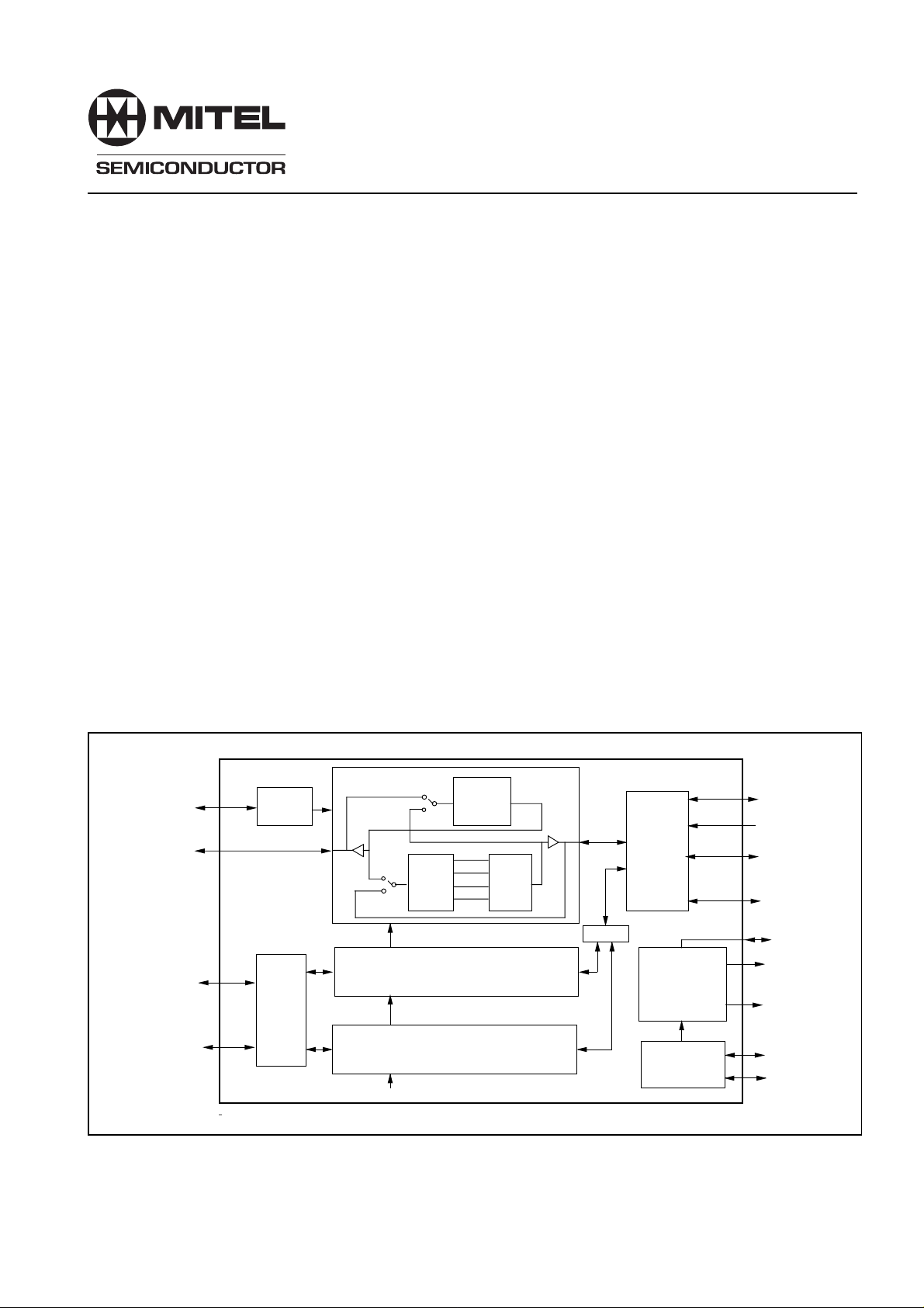
The VP520S is designed to convert 16 bit multiplexed
luminance and chrominance data between CCIR601 and CIF/
QCIF resolutions. Vertical and horizontal FIR filters are provided, with the vertical filters supported by on chip line stores.
The coefficients used by the filters are user definable, and are
down loaded from an independent host data bus. An internal
address generator supports an external DRAM frame store,
and also provides line to macroblock conversion.
When producing CIF or QCIF video the horizontal filters
precede the vertical filters, and are provided with between 8
and 16 taps. The vertical filters are provided with four CIF line
delays which allow a 5 tap filter to be implemented. When
producing QCIF the available RAM is used to provide six line
delays, which thus allows 7 tap filters to be used.
When the device is producing CCIR601 video, the incoming data must be in macroblock format, and the vertical filters
precede the horizontal filters The inputs are firstly written to a
external CIF sized frame store, and are read out in line format.
The VP520S will support two complete frame stores, and
allows the CIF/QCIF data to be read out twice in order to
produce two interlaced fields of video.
The VP520S supports the conversion between CIF/QCIF
and NTSC video. An extra line is produced for every five lines
when producing CIF data, and one line in six is removed when
producing NTSC video. Poly phase filters are used to provide
the correct decimation and interpolation ratios.
HOST
BUS
8 BIT
LUMINANCE
8 BIT
CHROMINANCE
CREF
COEFF
STORE
MUXING
MUXING
FILTER BLOCK
Horizontal
FOUR
LINE
DELAYS
FILTER BLOCK
FILTER BLOCK
Filters
Fig 1 : Simplified Block Diagram
Vertical
Filters
MUX
VP520S
INPUT/
OUTPUT
FIFO
RAM ADDRESS
GENERATOR
SUPPORTING
LINE TO BLOCK
CONVERSION
SYNC
GENERATOR
MACROBLOCK
STROBE
REQ BLKS
8 BIT
MACROBLOCK
BUS
16 BIT
FRAME STORE
BUS
FRAME START
/ READY
ADDRESS
CONTROL
HREF
VREF
1
VP520S
PIN DESCRIPTION
NAME TYPE FUNCTION
Y7:0 I/O Luminance input or output bus
C7:0 I/O Chrominance input or output bus
M7:0 I/O Macroblock input or output bus
D15:0 I/O 16 bit data bus for DRAM frame store
A7:0 O Multiplexed address bus to the DRAM
A8 O Most sig address bit or second CAS
RAS O Row strobe for the DRAM's
CAS O Column strobe for the DRAM's
R/W O Read/ write signal to the DRAM's
HREF I/O Horiz. reference in or horiz. sync out
VREF I/O Vertical reference in or vertical sync out
CREF I/O CREF in or CREF out
FREF I/O Field Indicator in or out
HBLNK O Horizontal Blanking output
CSYNC O Composite sync output in free run mode
CLMP O Defines a black level clamping period
for A/D converters
VRST Frame start identifier. If FRST is low
then a low going edge will reset the
internal sync generator.
FRST Field identifier
REQYUV I Request macroblocks from encoder
MCLK I/O Macroblock I/O strobe
FSIG I/O Frame start/ ready signal
SCLK I System Clock. 27MHz in PAL/NTSC
systems
HD7:0 I/O Host data bus
HA3:0 I Host controller address bits
RD I An active low host read strobe
WR I An active low host write strobe
CEN I An active low enable for the strobes
RST I Power on reset
TDI I JTAG I/P data
TDO O JTAG O/P data
TMS I Test mode select
TCK I JTAG clock
TRST I JTAG reset
TOE I When high all O/P's are high
impedance
NOTE:
"Barred" active low signals do not appear with a bar in the main
body of the text.
VIDEO COMPRESS MODE ( DECIMATE )
This mode is used when CCIR601 video is to be converted
to CIF or QCIF spatial resolution prior to compression. Incoming luminance and chrominance data does not need any prior
buffering, but must meet the timing requirements given in
Figure 2. A bit in Control register 1 allows the Cb component
to precede the Cr component if necessary. This data is passed
through vertical and horizontal decimating filters before it is
stored in an external frame store. When a complete field has
been decimated it is read out in macroblock format and
transferred to the next system component.
In this mode HREF, VREF, and FREF are normally inputs
which are used to reference active video with respect to video
synchronization pulses. The active going edges are used
internally, and these must meet the set up time with respect to
the system clock as given in Figure 2. Stable inputs are
needed with no jitter due to asynchronous pixel clocks, but
when this is not possible an external FIFO can be used plus
two extra signals as described later. The reference inputs
need only stay active for one system clock period. Note that
the active going edges for HREF and VREF can individually
be defined to be high going or low going, through two bits in
Control Register 0. Also note that CREF is always an input and
is used as a qualifier for SCLK. The actual edges of CREF are
not used.
The internal sync generator can still be used in this mode,
if there is a need to supply sync to the video source. The HREF
and VREF pins are then used to output HSYNC and VSYNC.
Composite sync is supplied on the CSYNC pin.
In addition the CLMP pin provides a pulse [13 SCLK's
wide] which can be used to DC restore the black level in an A/
D converter. It is active high during the back porch.
The horizontal blanking output (HBLANK) defines when
the device expects the first pixel in a line to be supplied, and
is derived from the user supplied HREF input. The delay
between HREF and HBLANK is user definable in multiples of
CREF periods. If the defined value is zero then the HREF input
must be horizontal blanking with the minimum set time specified. The HBLANK output is then not defined.
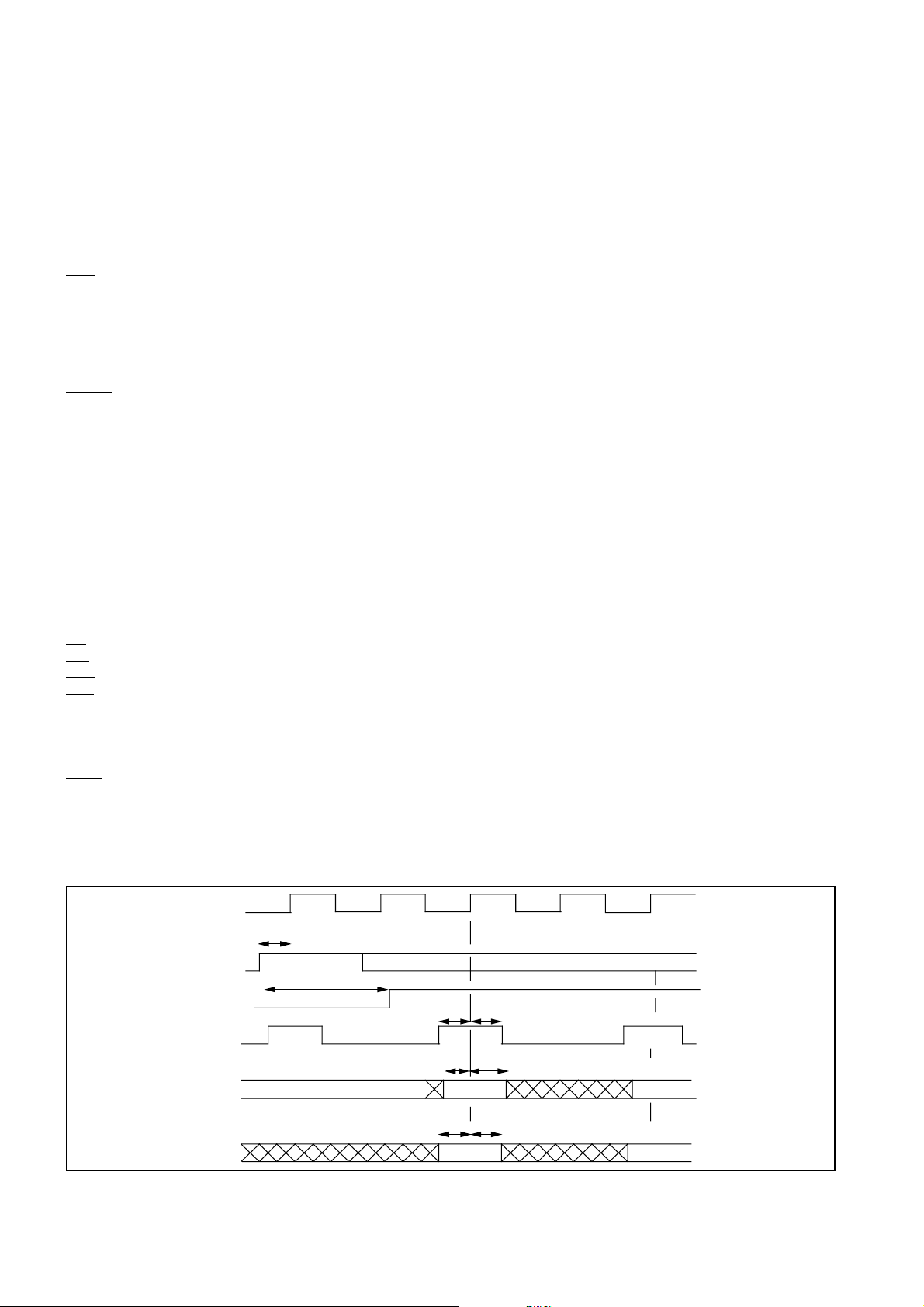
All data changes are referenced to the system clock. The
edge actually used is indicated by the CREF input signal,
which has a period of double the clock period. The VP520S will
strobe in data on the rising edge of the system clock which
occurs whilst CREF is high.
INPUT
CLOCK
10ns min
HREF
INPUT
HBLNK
O/P
CREF
INPUT
LUM
INPUT
CHROM
INPUT
PROGRAMMED DELAY
2ns
10ns
min
min
10ns
min
2ns
10ns
min
min
First Cr Comp.
2ns
min
Second I/PFirst I/P
First Cb Comp.
Fig 2 : Luminance and chrominance inputs in the decimate mode.
2
VP520S
The first video line to be filtered and stored will be derived
from the vertical reference input ( VREF). The user can choose
the number of transitions of the HREF input which must occur,
after VREF has gone active, before starting the filter operation. Data is then not written to the DRAM until after the
pipeline delay through the filters.
The VP520S only expects to use one field of CCIR601
video, which can be selected by the FREF input or internal
logic. A bit in Control Register 1 ( Internal / External Field
Detect ) determines which option is to be used. An additional
Field Select Bit determines whether the field selected should
correspond to FREF being high or low. When the Field Select
Bit and the input are at the same logical level then that field is
used. Note that FREF transitions must be coincident with
active going VREF transitions.
Internal logic is provided which determines the field ( Field
1 ) in which VREF goes active in less than half a line period
after the HREF input last went active.The half line period is
determined by VREF going active between 1 and 432 CREF
qualified SCLK edges after HREF went active (1-429 in NTSC
mode). Note that coincident VREF and HREF edges will
indicate this field on the first CREF qualified SCLK edge.
This logic is used, rather than the FREF input, when the
Internal / External Field Detect Bit is low. Field 1 is selected
when the Field Select in Control register 1 is low, and Field 2
is used when the bit is high.
In the Split Screen mode this logic is overridden, and both
fields are actually used. External logic is assumed to switch
between two sources of video, one for each field. The internal
DRAM address generator is modified such that half area
pictures from the centre of each source are actually stored as
CIF/QCIF data. The first line used in each field will be 72 line
delays in addition to the number which has been defined by the
user. The split screen option is not supported in the QCIF
mode of operation, and a reset is needed after a mode change
in CIF.
The VP520S will insert zero's into the line delays during
vertical blanking. This ensures that all the filter accumulators
are cleared and the edges of the picture are correctly processed. The horizontal filters always give the required results
since four decimated values are ignored at either side of the
picture.
Incoming luminance data could have a black level of 16,
which will be shifted if the filter coefficients are not chosen to
exactly give a gain of unity. A Control Bit is thus provided,
which when set causes 16 to be subtracted from incoming
luminance. A black level of zero will then stay as zero throughout the filter operation. At the output of the filters 16 is always
added to the results, regardless of the state of the Control Bit.
Saturation logic ensures that these addition / subtraction
operations do not produce negative results or values greater
than 254.
A Control Bit is also provided which selects between colour
difference inputs and true Cr Cb chrominance values. Cr Cb
values are 8 bit positive only numbers, with black levels of 128.
These must be converted to two's complement signed numbers by subtracting 128, thus giving a black level of zero
through the filters. The outputs of the filters are always
converted to positive only Cr Cb values by adding 128 to the
results, regardless of the state of the Control Bit.
COPING WITH SYNC JITTER
When input syncs to the VP520S have jitter, due to the use
of a composite video decoder which does not produce a line
locked clock, it is necessary to use an external FIFO line
buffer. For this reason the VP520S supports a system in which
external line buffer writes are controlled by the video source
and line reads are controlled by the VP520S. The VP520S in
the decode loop is assumed to be supplying sync to the
VP520S in the encode loop, but the sync generator must be
reset at the start of a frame to be in step with the video source.
Two pins have been supplied to support this situation, namely:
VRST - pin 34, and FRST - pin 36. The falling edge of VRST
(frame start identifier) when FRST (field identifier) is low
identifies the start of the frame. These two inputs can typically
be supplied by the Brooktree Bt812 Composite Video Decoder. Note that Host Address 3 must be programmed with
the value 02 Hex to enable the reset operation.
CIF/QCIF MACROBLOCK OUTPUTS
When producing decimated CIF/QCIF data in macroblock
format, the device raises a flag when a frame of data is ready
for reading from the frame store ( FSIG ). The FSIG pin is
automatically configured as an output in the decimate mode,
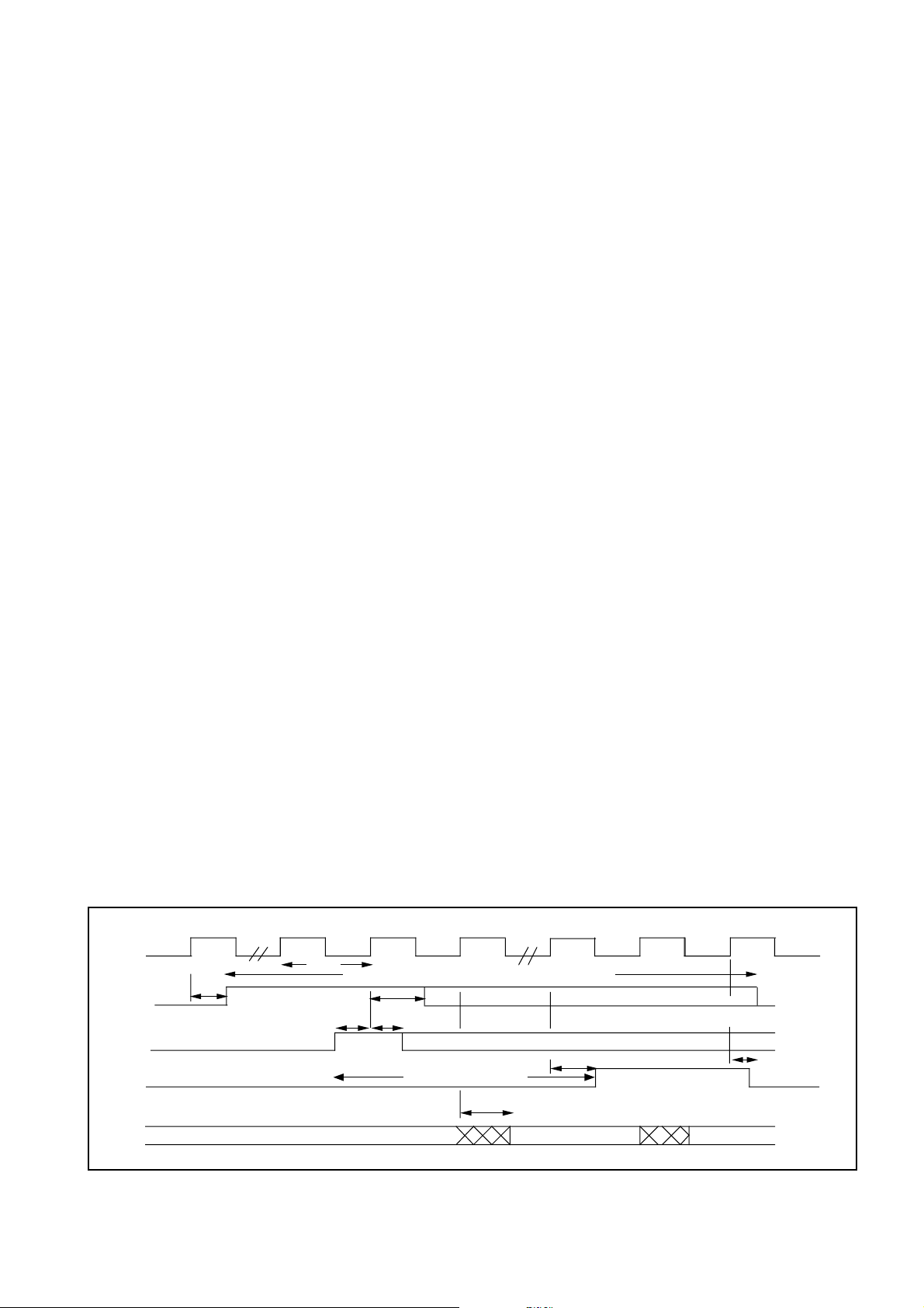
but will only stay active (high) for the time given in Figure 3. If
a Request Macroblock response (REQYUV) is not obtained
during this period, then FSIG will be taken low and the frame
of data presently available will be ignored. It will go high again
when a new frame of data is available.
SYSCLK
FSIG
O/P
REQYUV
I/P
MCLK
O/P
DATA
O/P
20ns
max
33ns min
Stays high for 11440 (NTSC) or 13284 (PAL) SCLKs if REQYUV not received
20ns max
10ns
2ns
min
min
60 SYSCLK Max , 10SYSCLK Min
20ns max
Fig 3 : Macroblock Output Timing
20ns max
First O/P Valid O/P Valid
20ns max
3
VP520S
-
-
-
-
-
-
-
FSIG
I/P
MCLK
DATA
I/P
40ns min
I/P
10ns min 2ns min
4SCLK min
40ns min
Second I/PFirst I/P
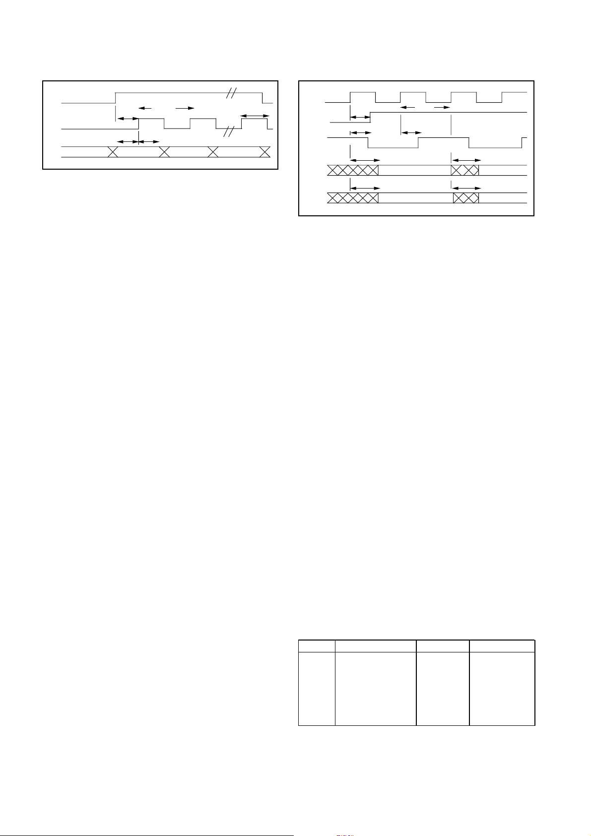
Fig 4 : Macroblock Input Timing
When it receives a REQYUV response from the next
system component, it starts to output a macroblock by using
an output strobe derived by dividing down the clock input.
Detailed timing is given in Figure 3. This strobe only occurs
when data is available at the output pins and at a rate of
SYSCLK/4. The 'Request Macroblock' flag must go inactive
and then active again before a further macroblock is made
available.
The Frame Ready flag is only available on the output pin
if the Frame Enable Bit is set in Control Register 1. Through
this control bit a host controller is able to determine whether a
new frame is to be compressed and transmitted. In an alternative arrangement the control bit can be permanently set, and
the Frame Ready Flag is then used as an interrupt to the host
controller. It then generates a signal which is used as the
Frame Ready signal for the next device.
The following sections describe this interface as it applies
to the VP2611 H261 Video Encoder.
TRANSFERING MACROBLOCKS TO THE VP2611
When the VP520S has stored a complete field of decimated video in the DRAM, it raises a Frame Ready Flag ( FSIG
). If the bit in Control Register 1 does not inhibit the output, this
flag becomes the FRMIN input on the VP2611. This responds
to the FRMIN input by generating a Request for Macroblock
Data ( REQYUV ). The VP2611 MUST then receive a complete macroblock ( 384 bytes ) within 1870 cycles of the
system clock. When the VP520S is producing decimated CIF/
QCIF data, writing line data to the DRAM has priority, and only
four macroblock read operations are possible in every 32
clock cycles i.e. one read takes eight cycles. These, however,
are 16 bit word operations and it thus requires 384 x 8/2 = 1536
cycles to output the data. In addition there is a maximum delay
of 60 clock periods from receiving REQYUV to producing the
first output strobe (MCLK). This is still well within the time
available.
The four 16 bit words are stored in the VP520S and
transmitted to the VP2611 as eight bytes using a strobe
( MCLK ) derived from the system clock. This is only present
when valid data is available, and it drives the PCLK input on
the VP2611.
It takes the VP2611 almost exactly all the available time at
30 Hz frame rates to process all the macroblocks. After a field
time ( half an interlaced frame ) the VP520S will start to write
new data to the DRAM, and data could be overwritten during
the last macroblocks. Since there is available space in the
DRAM, a small address offset is used between video fields to
avoid this problem.
INPUT
CLOCK
HBLANK
O/P
CREF
O/P
LUM
OUTPUT
CHROM
O/P
20ns
max
20ns max
20ns max
20ns max 20ns max
33ns min
20ns
max
First O/P Valid
First Cr Component Valid
20ns max
Second O/P Valid
First Cb
Fig 5 : Luminance and Chrominance Output Timing
INTERPOLATE MODE
In this mode the VP520S expects to receive CIF/QCIF
data in macroblock format, which it then writes to an external
frame store. This is then read back in line format and passed
through vertical and horizontal interpolating filters to produce
two fields of CCIR601 video. Detailed input timing is given in
Figure 4.
FSIG automatically becomes an input which is used to
identify the start of a frame and to reset the internal address
counter. FSIG must stay high until a complete CIF/QCIF frame
has been received ( internal logic counts macroblocks ). If
FSIG goes low early then the complete frame will be ignored,
and the previously received frame will continue to be displayed.
An input strobe, derived by dividing the system clock by
four, must also be provided in order to input data. This must
only be present when valid data is available on the input pins.
Incoming macroblocks are byte wide, and these are internally
buffered to allow four 16 bit words to be written to the DRAM
every 32 system clock cycles. This is equivalent to a byte input
rate of SCLK/4 which must not be exceeded.
The CIF frame store is double buffered such that a new
frame can be received whilst the previous one is being
displayed. In fact the use of 256K x 16 DRAM's gives sufficient
capacity for more than three complete CIF frames, and the
internal address generator will simply roll around to make full
use of the available space.
Once a complete CIF/QCIF frame has been received, it will
normally be used to generate two interlaced PAL or NTSC
fields. These fields continue to be re-generated until a complete new CIF frame has been received. The rate of receiving
frames depends on the transmission bandwidth, but the
maximum rate is 30 Hz. The changeover to the newly received
frame will occur when the VP520S has finished generating
any one of the pair of interlaced fields for display, it does not
SYMBOL PARAMETER MINIMUM MAXIMUM
t RAC Access time from RAS
t CAC Access time from CAS
t RP RAS precharge time 50ns or under
t CP CAS precharge time 12ns or under
t RAS RAS pulse width 80ns or under
t CAS CAS pulse width 50ns or under
t REF Time between
complete refreshes
105ns or under
25ns or under
4 ms or over
(8 ms with 256k x n)
N.B. All times are quoted assuming 27MHz operation. For lower clock
frequencies increase the above values proportionately.
4
Table 1. External DRAM Timing Requirements
VP520S
necessarily have to have generated two interlaced fields from
the received frame. If the VP520S is receiving frames at the
full CIF 30 Hz frame rate but only displaying PAL frames at 25
Hz, then periodically one of the PAL frames ( comprising two
interlaced fields at 50 Hz ) will be generated from two received
CIF/QCIF frames. An incoming CIF/QCIF frame will always be
used since the interlaced field rate is always greater than 30
Hz in either PAL or NTSC.
The data is read from the frame store such that interpolated data becomes available after programmed delays referenced to the VREF and HREF signals. Six bits are available
to define the line delay, and ten are provided to define the
delay from HREF in CREF periods. The actual delays are
greater than the programmed values because of the internal
pipeline delays, which are also mode dependent.
HREF and VREF can either be user supplied inputs, or are
generated internally from a PAL/NTSC timing generator. A bit
in Control Register 0 determines this option, and when the
internal generator is specified the HREF pin becomes an
output which supplies horizontal sync and the VREF pin
supplies vertical sync. A composite sync output is also provided for system level use. In this mode the VREF and HREF
signals used internally are effectively vertical and horizontal
sync, and the programmed delays should be chosen to reflect
this condition.
The signals provided from the internal timing generator
allow the VP520S to drive the VP510 Colour Space Converter
and an RGB monitor. Detailed output timing is given in Figure
5. Note that the chrominance order can be changed. Alternatively they can be used to drive off the shelf composite video
encoders.
External chrominance data can have a zero colour difference value of either 0 or 128. This is defined using the
Chrominance Control Bit. Where 128 is the zero colour
difference value, 128 will be subtracted from incoming
chrominance data and 128 will be added to output chrominace
data. Output values will be limited to lie in the range 16 to 240.
External luminace data can have a black luminace level of
either 0 or 16. This is defined using the Luminace Control Bit.
Where 16 is the black value, 16 will be subtracted from
incoming luminace data and 16 will be added to output
luminace data. Output values will be limited to lie in the range
16 to 235.
The data stored in the CIF frame store will not contain the
black levels normally present during horizontal and vertical
flyback. This is inserted by the VP520S at the appropriate
times in order to ensure that the correct filter operation occurs
at the edges of the picture. In addition to these black levels
during flyback, a bit in Control Register 1 allows all active video
to be replaced by a fixed colour. This colour is user definable
through YUV values in three registers.
FRAME STORE INTERFACE
All read and write operations to the external DRAM frame
stores are based on the use of fast page mode with 13.5 MHz
CAS cycles. Internally a 54 MHz clock is produced from the
27MHz System clock, and this determines the minimum time
interval which can be used in the generation of pulses and
defining precharge times. Any DRAM used must meet the
timing constraints given in Table 1.
Reading and writing rates dictate the need for a 16 bit data
interface, and line data is re-organized to allow a 16 bit word
to consist of either two luminance values or two chrominance
values. This gives compatibility with the macroblock requirements since a sub block is either all chrominance or all
luminance data. Reading or writing macroblock data requires
jumps between pages, but four words can always be read or
written using fast page mode.
Read and write operations must be timeshared to meet the
requirements of the system. This time-sharing is based on the
use of 16 cycles of the 13.5 MHz clock. When reading or
writing line data to the store, 10 cycles are used for eight
words, and six cycles are left free for four exchanges with the
encoder or decoder. The additional cycles are needed when
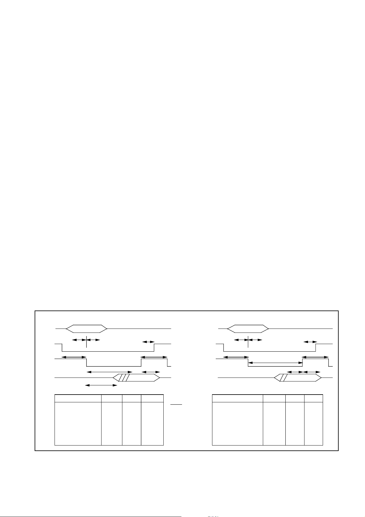
ADDRESS
CHIP
SELECT
READ
STROBE
DATA
OUT
READ CYCLE
Tas
Tah
Trs
CHARACTERISTIC
Addresss Set Up Time
Address Hold Time
Cip Select Set Up Time
Chip Select Hold Time
Strobe Inactive Time
Data Access Time
Delay to O/P's low Z
Delay to O/P's high Z
Tac
Tlz
SYMBOL
Tas
Tah
Trs
Tsh
Tri
Tac
Tlz
Thz
MIN
10ns
10ns
10ns
2ns
Øns
2Øns
Tsh
Tri
Thz
Data
Valid
MAX
ADVANCED DATA
20 +3Øns
25ns
NOTE
Ø is the period of the
input clock
Fig 6 : Host Interface Timing
ADDRESS
CHIP
SELECT
WRITE
STROBE
DATA
IN
CHARACTERISTIC
Addresss Set Up Time
Address Hold Time
Chip Select Set Up Time
Chip Select Hold Time
Strobe Inactive Time
Strobe Active Time
Data Set Up Time
Data Hold Time
Tas
Tws
WRITE CYCLE
Tah
Twa
SYMBOL
Tas
Tah
Tws
Tsh
Twi
Twa
Tds
Tdh
Tds
MIN
10ns
10ns
10ns
2ns
1Øns
3Øns
10ns
10ns
Data
Valid
Tsh
Twi
Tdh
MAX
5
 Loading...