MITEL VP310CGGQ1R Datasheet

VP310
Satellite Channel Decoder
Preliminary Information
SHORTFORM TECHNICAL MANUAL DS5155 -1.00 21/04/99
Ordering Information
VP310 - Key Features
•
Conforms to EBU specification for DVB-S and DirecTV specif ication for DSS.
•
On-chip digital filtering supports 1 to 45MBaud Symbol rates.
•
On-chip 6-bit 60 or 90MHz dual-A DC.
•
High speed scanning mode for blind symbol rate and code rate ac quisition.
•
Up to ± 15MHz LNB frequenc y tracking.
•
Fully digital t iming and phase recovery loops.
•
High level soft ware i nterface for mini mum development time.
•
DiSEqC™ v1.1: contr ol outputs for full cont r ol of LNB and dish.
Applications
•
DVB 1 to 45MBaud compliant satellite receivers.
•
DSS 20MBaud com pliant satellite receivers.
•
SCPC receivers. (Single Channel Per Carri er )
•
SMATV trans-modulators. (Single Master Antenna TV)
•
LMDS. (Local M ultipoint Distribution S er vice)
•
Satellite PC applications.
VP310 CG GQ1R
The VP310 is a QPSK/BPSK 1 to 45MBaud demodulator and channel decoder for
digital satellite television transmissions to the European Broadcast Union ETS 300 421
specification. It receives analog I and Q signals from the tuner, digitises and digitally
demodulates thi s signal, and i mplements the com plete DVB/DSS FE C (Forward Error
Correction), and de-scrambling function. The output is in the f orm of MPEG2 or DSS
transport stream data packets. The VP310 al so provides automat ic gain control t o the
RF front-end devi c es.
The VP310 has a serial I²C port interface to the control microprocessor. Minimal
software is required to control the V P310 because of the buil t in automat ic search and
decode control functions.
VP310 PRELIMINARY DATA
y
y
g
g
Overview
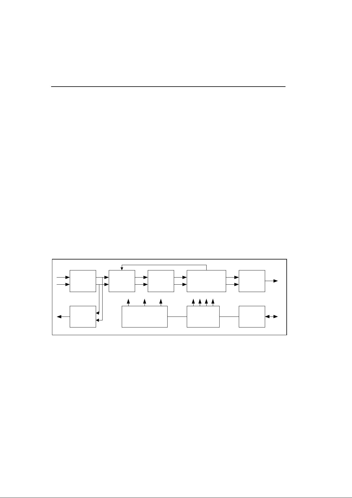
The VP310 is a QPSK/BPSK 1 to 45MBaud demodulator and channel decoder
for digital satellite television transmissions compliant to both DVB-S and DSS
standards and other systems, such as LMDS, that use the same architecture.
A Command Driven Control (CDC) system is provided making the VP310 very
simple to program. After the tuner has been programmed to the required
frequency, to acquire a DVB transmission, the VP310 requires a minimum of
five registers to be written, see Figure 15 on page 19. Activity flow diagrams for
initialisation and basic channel change are included in section 2.
The VP310 provides a monitor of Bit Error Rate after the QPSK module and
also after the Viterbi module.
For receiver installation, a high speed scan or ‘blind search’ mode is available.
This allows all signals from a given satellite to be evaluated for frequency,
symbol rate and convolutional coding scheme.
I I/P
Q I/P
2
Dual ADC
Analo
AGC
control
De-rotator
Clock Generation
Figure 1. VP310 Functional Block Diagram.
Decimation
Filteriin
Timing recover
Matched filter
Phase recover
Acquisition
Control
DVB
DSS
FEC
I²C
Interface
MPEG/
DSS
Packets
Bus I/O

VP310 PRELIMINARY DATA
Additional Features
•
I²C bus micr opr ocessor int erface.
•
All digit al clock and carrier recovery.
•
On-chip PLL clock generation using low cost 10 t o 15MHz crystal.
•
3.3V operation.
•
80 pin MQFP package.
•
Low external component count.
•
Commerci al t em peratur e range 0 to 70°C.
Demodulator
•
BPSK or QPSK pro gramm ab le.
•
Optional fast acquisition m ode for l ow symbol rates.
Viterbi
•
Programmable decoder rates 1/2, 2/3, 3/ 4, 5/6, 6/7, 7/8.
•
Constraint length k=7.
•
Trace back depth 128.
•
Extensive SNR and BER monitors.
De-Interleaver
•
Compliant wi t h DVB and DSS standards.
Reed Solomon
•
(204, 188) for DVB and (146,130) for DSS.
•
Reed Solomon Bit-error-rate monitor to indicate Viterbi performance.
De-Scrambler
•
EBU specification De-scrambler for DVB m ode.
Outputs
•
MPEG transport parallel & serial output.
•
Integrated MPEG2 TEI bit processing for DVB only.
Application Suppor t
•
Channel decoder system evaluation board.
•
I²C interface board to PC.
•
Wi ndows based evaluation softwar e.
•
ANSI C generic software.
•
Application support help desk via emai l / telephone.
3

VP310 PRELIMINARY DATA
PLEASE NOTE: This manual has the following convention:
All numerical values are shown as decimal numbers, unless oth erwise defined .
1. FUNCTIONAL DESCRIPTION
1.1 Introduction
VP310 is a single-chip variable rate digital QPSK/BPSK satellite demodulator and channel
decoder. The VP310 accepts base-band in-phase and quadrature analog signals and delivers an
MPEG or DSS packet data stream. Digital f iltering in VP310 removes the need for any external
anti-ali as filtering for all sym bol rates from 1 to 45Mbaud. Frequency, tim ing and carrier phase
recovery are all digital and the only feed-back to the analog front-end is for automatic gain
control. The digital phase recovery loop enables very fine bandwidth control that is needed to
overcome performance degradation due to phase and thermal noise.
All acquisit ion algorithms are buil t into the VP310 controller. The VP310 can be operated in a
Command Driven Control (CDC) mode by specifying the Symbol rate and Viterbi code rate.
There is also a provision for a search for unknown Symbol rates and Viterbi code rates.
1.2 Analog-to-Digital Converter
The VP310 contains dual 6-bit A/D converters which each sample a 1.0Vpp singl e-ended analog
input at up to 90MHz. The fixed rate sampling clock is provided on-chip using a pr ogramm able
PLL needing only a low cost 10 to 15MHz crystal. Dif ferent crystal frequencies can be combined
with different PLL ratios, depending on the maximum sym bol rate, all owing a fl exible approach to
clock generation.
1.3 QPSK Demodulator
The demodulator in the VP310 consists of signal ampli t ude offset compensation, f r equency offset
compensation, decim at ion filtering, carr i er recovery, symbol recovery and matched filtering.
The decimati on filters give continuous operation fr om 2Mbits/ s to 90Mbits/ s all owing one receiver
to cover the needs of the consumer market as well as the single carrier per channel (SCPC)
market with the same components without compromising performance, that is, the channel
reception is within 0.5dB from t heory. For a given Symbol rate, control algorithm s on the chip
detect the number of decimation stages needed and switch them in automati cally.
The frequency offset compensation circuitry is capable of tr acking out up to ± 15MHz frequency
offset. This all ows the system to cope with relatively l arge frequency uncertainties i ntroduced by
the Low Noise Block (LNB). Full control of the LNB is provided by the DiSEqC outputs from the
VP310. Horizontal / Vertical polari sati on and an inst ructi on m odulat ed 22kHz signal are available
under register control. All DiSEqC v1.1 funct ions are implemented on the VP310.
4

VP310 PRELIMINARY DATA
An internal state machine that handl es all the demodulator f unctions control s the si gnal tr acking
and acquisition. Various pre-set modes are available as well as blind acquisition where the
receiver has no prior knowledge of the received signal. Fast acquisition algorithms have been
provided for low Symbol rate applications. Full interacti ve control of the acquisi tion function i s
possible for debug purposes.
In the event of a signal fade or a cycle slip, Q PSK demodul ator al lows suff ici ent tim e for the FEC
to re-acquire lock, for example, via a phase rotation in the Viterbi decoder. This is to m inimise the
loss of signal due to the signal fade. Only i f the FEC fails to re-acquir e lock for a long period
(which is progr ammable) would Q PSK try to re-acquire the signal.
The matched filter is a root-raised-cosine filter with either 0.20 or 0.35 roll-off, compliant with
DSS and DVB standards. Although not a part of the DVB standard, VP310 allows a roll -off of
0.20 to be used with other DVB parameters.
An AGC signal is provided to contr ol the signal levels in the tuner section of the receiver and
ensure the signal level fed to the VP310 is set at an optim al value under all reception conditions.
The VP310 provides comprehensive information on t he input signal and the state of the various
parts of the device. This information includes Signal to Noise Ratio (SNR), signal level, AGC
lock, tim ing and carrier lock si gnals. A maskable interrupt output is availabl e to inform the host
con tro ller when ev ents occur.
1.4 Forward Error Correction
The VP310 contains FEC blocks to enable error correction for DVB-S and DSS transmissions.
The Viterbi decoder block can decode the convolutional code with rates 1/2, 2/3, 3/4, 5/6, 6/ 7 or
7/8. The block features automat ic synchronisation and aut omatic code rate detection. The trace
back depth of 128 provides better performance at high code rates and the built - in synchronisation
algorithm allows the Viterbi decoder to lock onto signals with very poor signal-to-noise ratios.
Viterbi b it error rate monitor p rovides an indication of the error rate at QPSK o u t p ut.
The 24-bit error count register in t he Viterbi decoder allows the bit error rate at the output of t he
QPSK demodulator to be monitored. The 24-bit bit error count register in the Reed-Solomon
decoder allows the Viterbi output bi t error rate to be monitor ed. The 16-bit uncorrectable packet
counter yields information about the output packet error rate. These three monitors and the
QPSK SNR register all ows the perform ance of the device and its i ndiv idual com ponents, such as
the QPSK demodulator and the Viterbi decoder, to be monitored extensively by the external
microprocessor.
The frame/byte align block features a sophisti cated synchronisation algori thm to ensure reliable
recovery of DVB and DSS framed data streams under worst case signal conditions. The deinterleaver uses on-chip RAM and is compatible with the DVB and DSS algorithm s.
The Reed-Solomon decoder is a truncated version of t he (255, 239) code. The code block size is
204 for DVB and 146 for DSS. The decoder provides a count of the number of uncorrectable
blocks as well as the number of bit errors cor rected. The latter gives an indicat ion of the bit error
rate at the output of the Viterbi decoder.
5
VP310 PRELIMINARY DATA
In DVB mode, spectrum de-scram bling i s performed com patible wi th the DVB specif ication. The
final output is a parallel or serial transpor t data stream; packet sync; data clock; and a block error
signal. The data clock may be inverted under software control.
1.4.1.1 Viterbi error count measurement
A method of estim ating the bit error rate at the output of the QPSK block has been provided in
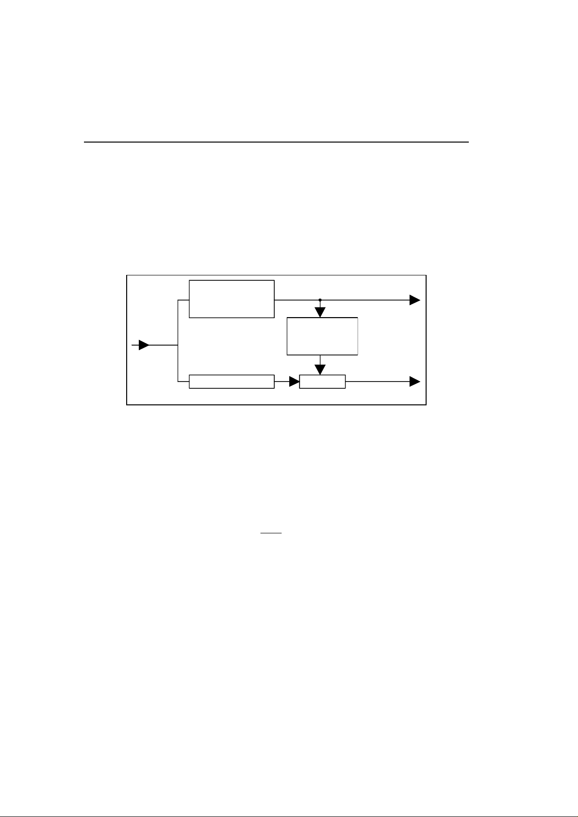
the Viterbi decoder. The incoming data bit stream is delayed and compared with the re-encoded
and punctured version of the decoded bit stream to obtain a count of errors see Figure 2 below.
VITERBI
DECODER
VITERBI
ENCODER
DELAY COMP
DATA BIT STREAM
ERROR COUNT
Figure 2. Viterbi block diagram.
The measurement system has a programmable register to determine the number of data bi ts (the
error count period) over which the count is being recorded. A read register indicates the error
count result and an interrupt can be generated to inform the host m icroprocessor that a new
count is availabl e.
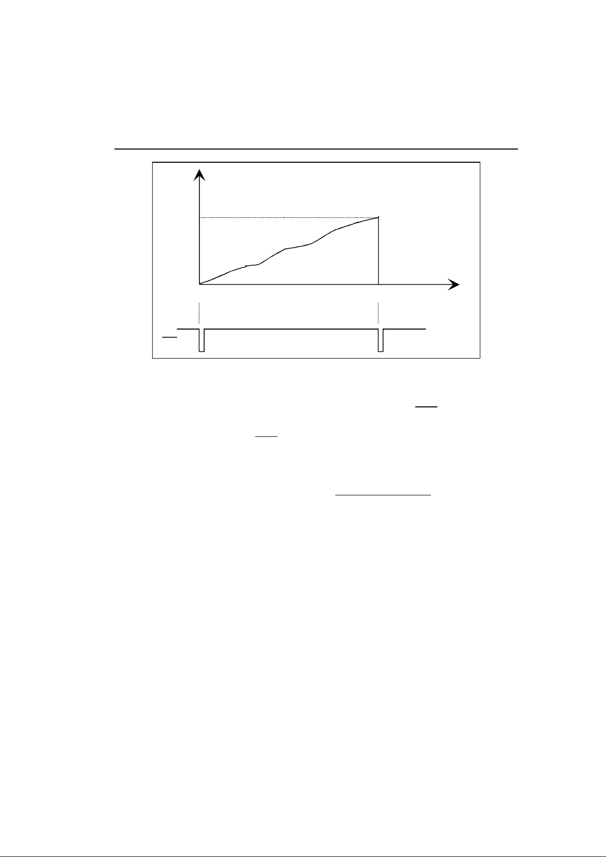
The VIT_ERRPER H-M-L group of three registers is programm ed with required number of data
bits (the error count period) (VIT_ERRPER[23:0]). The actual value is four times
VIT_ERRPER[23:0]. The count of errors found duri ng this period is l oaded by the VP310 i nto the
VIT_ERRCNT H-M-L tri o of registers when the bit count VIT_ERRPER[23:0] i s reached. At t he
same tim e an interrupt is generated on the IRQ
register enables the interrupt. Reading the regist er does not clear VIT_ERRCNT [23: 0], it is onl y
loaded with the error count.
line. Setting the IE_FEC[2] bit in the IE_FEC
6
VP310 PRELIMINARY DATA
ERROR
COUNT
VIT_ERRCNT[23:0]
0
0
IRQ
VIT_ERRPER[2 3:0]
Figure 3. Viterbi error count measurement.
Figure 3 above shows the bit errors rising until the maximum programmed value of
VIT_ERRPER[23:0] is reached, when an interrupt is generated on the IRQ
host microprocessor that a new value of bit error count has been loaded into the
VIT_ERRCNT[23:0 ] r egister. The IRQ
line will go high when the IE_FEC register is read by the
host micr opr ocessor.
DATA BITS
line to advise the
VIT_ERRCNT[23: 0] VIT_ERRPER[23:0]
The error count may be expressed as a ratio:
VIT_ERRCNT[23:0]
VIT_ERRPER[23: 0] * 4
1.4.1.2 Viterbi error count coarse indication
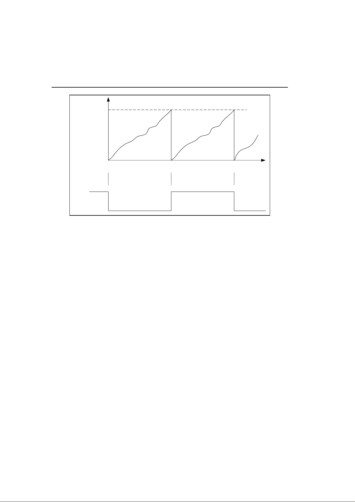
To assist in the process of aligni ng the receiver dish aerial, a coarse indication of t he number of
bit errors being received can be provided by monitoring the STATUS line with the f ollowing set up
conditions.
The frequency of the output waveform will be a function of the bit error count (triggering the
maximum value programmed into t he VIT_MAXERR[7:0] register and the dish ali gnment on the
satellite. This VIT_MAXERR mode is enabled by setting the FEC_STAT_EN register bit B0.
Figure 4 on page 8 shows the bit errors rising to the m aximum val ue program m ed and tr iggering
a change of state on the STATUS line.
The output signal will be in the audio frequency range.
7
VP310 PRELIMINARY DATA
VITERBI
COURSE
BIT
ERROR
COUNT
0
0
STATUS
Figure 4. Viterbi error count coarse indication.
VIT_MAXERR[7:0]
DATA BITS
1.4.2 The Frame Alignment block
The frame alignm ent algor i thm detects a sequence of correctly spaced synchr onising bytes in t he
Viterbi decoded bit-stream and arranges the input int o blocks of data bytes. Each block consists
of 204 bytes for DVB and 147 bytes for DSS. In the DSS mode, the synchronising byte is
removed from the data stream , so only 146 bytes of a block are passed to the next stage. The
frame alignment block also removes the 180° phase ambiguity not rem oved by Viterbi decoder.
1.4.3 The De-interleaver block
1.4.3.1 DVB
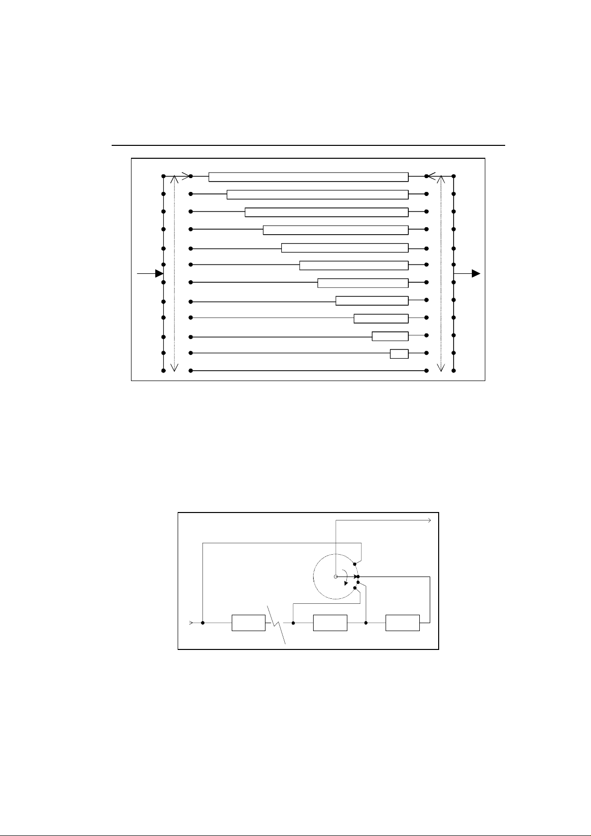
Before transmission, the data bytes are interleaved with each other in a cyclic pattern of twelve.
This ensures the bytes are spaced out to avoid the possibility of a noise spike corrupting a group
of consecutive message bytes. The diagram below shows conceptually how the convolutional deinterleaving system works. The synchronisation byte is always loaded into the First-I n-First-Out
(FIFO) m em or y i n br anch 0. The switch i s operated at regular byte intervals t o insert successively
received bytes into successive branches. After 12 bytes have been received, byte 13 is written
next to the synchronisation byte in branch 0, etc. In the VP310, this de-interleaving function is
realised using on-chip Random Access Memory (RAM).
8
VP310 PRELIMINARY DATA
Sync word r oute
17x11 byte s
17x10 byte s
17x9 bytes
17x8 bytes
17x7 bytes
17x6 bytes
17x5 bytes
17x4 bytes
17x3 bytes
17x2 bytes
17x1
0
1
2
3
4
5
6
7
8
9
10
11
one
byte per
position
0
1
2
3
4
5
6
7
8
9
10
11
Figure 5. DVB Conceptual diagram of the convolutional de-interleaver block.
1.4.3.2 DSS
Before transmission, t he data bytes are interleaved with each other in a cyclic pattern of t hirt een.
This ensures the bytes are spaced out to avoid the possibility of a noise spike corrupting a group
of consecutive message bytes. The diagram below shows conceptually how the convolutional deinterleaving system works. On the VP310, this funct ion is realised in the same Random Access
Memory (RAM) as used for DVB, but utilising different addressing algorithm.
Output
145
0
1
2
Input
12D12D12D
Figure 6. DSS Conceptual diagram of the convolutional de-interleaver block.
9

VP310 PRELIMINARY DATA
1.4.4 The Reed Solomon Decoder block
DVB and DSS data are encoded using shortened versions of the Reed-Solomon code of block
length 255, containing 239 message bytes and 16 check bytes, that is (255,239) with T = 8. Both
encoders use the same generator polynomial. The code block size for DVB is 204 and that for
DSS is 146. Hence DVB code is (204, 188) and DSS code is (146, 130), with both having T = 8.
The block structure of the DVB and DSS Reed-Solomon codes are as shown in Figure 7 and
Figure 8 on page 10.
The Reed-Solomon decoder can correct up to eight byte errors per packet. If there are more than
8 bytes containing errors, the packet is flagged as uncorrectabl e using the pin BKERR. In the
case of DVB the transport error indicator (TEI) bit of the MPEG packet is set to 1, if setting of TEI
is enabled.
Sync byte 187 bytes
Reed Solomon encoded block
Sync byte 187 bytes
MPEG transport packet
Figure 7. DVB block structure.
130 bytes
Reed Solomon encoded block
130 bytes
DSS transport packet
Figure 8. DSS block structure.
16 check bytes
16 check bytes
10
 Loading...