MITEL VP305, VP306 Datasheet

VP305/6
Satellite Channel Decoder
Preliminary Information
DM5009-1.0 09/07/98
MITEL CONFIDENTIAL INFORMATION
TECHNICAL MANUAL
This is an unpublished work the copyright in which vests in Mitel. All rights reserved.
The information contained herein is the property of Mitel and is supplied without liability for
errors or omissions. No part may be reproduced or used except as authorised by contract
or other written permission. The copyright and the foregoing restriction on reproduction
and use extend to all media in which the media may be embodied.
The VP305/6 is a decoder for digital satellite television transmissions to the European Broadcast
Union ETS 300 421 specification (ref. 1). They receive digitised I and Q signals from the tuner,
demodulate the QPSK data and provide a complete Forward Error Correction, (FEC) and descrambling function. The output is in the form of packetised MPEG2 transport stream data. The
VP305/6 also provides automatic gain control and synchronising signals to the RF front end
devices.
The VP305 has only a parallel interface port to the control microprocessor.
The VP306 has both a serial I²C port and a parallel interface port to the control microprocessor.

VP305/6 DRAFT - PRELIMINARY DATA
The duplication or disclosure of data contained on this sheet is subject to the restrictions
on the title page of this document.
2
CONTENTS.
1. FUNCTIONAL DESCRIPTION...............................................................................................7
1.1. System overview...........................................................................................................7
1.2. The QPSK Demodulator block......................................................................................9
1.2.1. Input requirements..............................................................................................10
1.2.3. Matched filters.....................................................................................................10
1.2.4. Decimation filters.................................................................................................10
1.2.5. Carrier frequency synchronisation ......................................................................11
1.2.6. Symbol synchronisation and tracking..................................................................12
1.3. The Viterbi Decoder block.............................................................................................13
1.3.1. Viterbi error count measurement.........................................................................14
1.3.2. Viterbi error count coarse indication....................................................................15
1.4. The De-interleaver block...............................................................................................16
1.5. The Reed Solomon block..............................................................................................18
1.6. The Energy Dispersal (descrambler) block...................................................................18
1.6.1. Output stage........................................................................................................19
1.7. Microprocessor interface...............................................................................................19
2. REGISTER DETAILS.............................................................................................................20
2.1. Parallel interface register map. .....................................................................................20
2.2. Serial interface register map. ........................................................................................23
2.3. BANK: Register bank address - Parallel mode only......................................................25
2.4. RADD: I²C Register address - Serial mode only...........................................................26
2.5. BANK 0: Monitor QPSK read registers..........................................................................27
2.5.1. ID: Identification register. ....................................................................................27
2.5.2. INT_QPSK: Interrupt for QPSK block, register....................................................27
2.5.3. INT_FEC: Interrupt FEC register.........................................................................28
2.5.4. STATUS: Status register.....................................................................................29
2.5.5. AGC_LVL: AGC loop voltage meter register.......................................................30
2.5.6. CR_VCOF U & L: Measured VCO frequency registers. ......................................30
2.5.7. IE_QPSK: Interrupt enable QPSK register..........................................................31
2.6. BANK 1: Program QPSK registers................................................................................ 32
2.6.1. SYM_CONFIG: Symbol configuration register....................................................32
2.6.2. SYM_RP: Symbol AFC reference period register............................................... 33
2.6.3. SYM_NF U & L: Symbol input nominal frequency registers................................33

DRAFT - PRELIMINARY DATA VP305/6
The duplication or disclosure of data contained on this sheet is subject to the restrictions
on the title page of this document.
3
2.6.4. SYM_RATIO: Symbol input decimation factor register.......................................34
2.6.5. AGC_REF: Reference AGC level registers. ....................................................... 34
2.6.6. AGC_BW: AGC estimation bandwidth register................................................... 35
2.7. BANK 2: Program QPSK registers................................................................................ 36
2.7.1. SCALE: IOUT and QOUT outputs, scale factor register.....................................36
2.7.2. SNR_THS: Signal to noise ratio estimator threshold register.............................36
2.7.3. CR_OFFSET: Carrier loop DC offset register..................................................... 37
2.7.3.1. Acquisition Phase..................................................................................38
2.7.3.2. Tracking Phase...................................................................................... 39
2.7.4. CR_RP: Carrier reference period register...........................................................39
2.7.5. CR_KP: Carrier loop filter gain (P term) register.................................................40
2.7.6. CR_KD: Carrier loop filter gain (D term) register................................................40
2.7.7. CR_THSL: Carrier lock detector threshold register............................................ 41
2.8. BANK 3: Program QPSK registers................................................................................ 42
2.8.1. CR_SWR: Carrier sweep rate register................................................................ 42
2.8.2. CR_USWL U & L: Carrier Upper sweep limit registers....................................... 43
2.8.3. CR_LSWL U & L: Carrier Lower sweep limit registers. ...................................... 44
2.8.4. CR_CONFIG: Carrier configuration register.......................................................44
2.8.5. CONFIG: Configuration register..........................................................................45
2.9. BANK 4: Monitor FEC read registers............................................................................ 46
2.9.1. VIT_ERR_C H & L: Viterbi error count registers................................................. 46
2.9.2. RS_UBC: Reed Solomon uncorrected block count register. .............................. 46
2.10. BANK 5: Program FEC registers. ................................................................................. 47
2.10.1. VIT_MODE: Viterbi mode register.....................................................................47
2.10.2. VIT_ERR H, M & L: Viterbi error period registers. ............................................48
2.10.3. VI_MAX_ERR: Viterbi maximum bit error count register. .................................48
2.10.4. VI_BER_PER: Viterbi bit error rate based synchronisation period register. .....49
2.10.5. VI_BER_LIM: Viterbi bit error rate based synchronisation limit register. .......... 49
2.11. BANK 6: Program FEC and general control registers..................................................50
2.11.1. VIT_CTRL1: Viterbi control synchronisation byte register 1 ............................. 50
2.11.2. VIT_CTRL2: Viterbi control synchronisation byte register 2 ............................. 51
2.11.3. IE_FEC: Interrupt FEC register......................................................................... 52
2.11.4. STAT_EN: Status enable register..................................................................... 53
2.11.5. GEN_CTRL: General control register. ..............................................................54

VP305/6 DRAFT - PRELIMINARY DATA
The duplication or disclosure of data contained on this sheet is subject to the restrictions
on the title page of this document.
4
2.11.6. GPP_CTRL: General Purpose Port control register..........................................54
2.11.7. RESET: Reset register......................................................................................55
2.12. BANK 7: Program test registers. ...................................................................................56
2.12.1. TEST1: Test 1 register - for diagnostic / qualification purposes only................56
2.12.2. TEST2: Test 2 register - for diagnostic / qualification purposes only................56
2.12.3. TEST3: Test 3 register - for diagnostic / qualification purposes only................57
3. MICROPROCESSOR CONTROL..........................................................................................58
3.1. I²C bus Interface............................................................................................................58
3.1.1. Examples of I²C bus messages: ........................................................................59
3.2. Parallel interface. ..........................................................................................................60
3.2.1. Examples of writing to and reading from the parallel interface. ..........................60
3.2.2. Parallel interface Write cycle description. ...........................................................60
3.2.3. Parallel interface Read cycle description............................................................63
4. TIMING INFORMATION.........................................................................................................65
4.1. I²C bus timing................................................................................................................65
4.2. Parallel interface Write cycle timing..............................................................................66
4.3. Parallel interface Read cycle timing..............................................................................66
4.4. Data input timing. ..........................................................................................................67
5. MPEG PACKET DATA OUTPUT...........................................................................................68
5.1. Data output format.........................................................................................................68
5.2. Data output timing.........................................................................................................70
6. VP305/6 OPERATING CONDITIONS....................................................................................71
6.1. Recommended operating conditions.............................................................................71
6.2. Electrical characteristics................................................................................................72
6.3. Crystal specification......................................................................................................73
6.4. Absolute maximum ratings............................................................................................73
6.5. Pinout description..........................................................................................................74
6.6. Alphabetical listing of the pinout....................................................................................77
6.7. Numerical listing of the pinout.......................................................................................78
7. REFERENCES.......................................................................................................................80
8. APPENDIX 1: FEATURES.....................................................................................................81
9. APPENDIX 2: LOCK ACQUISITION ALGORITHM. ...............................................................82
9.1. Pre conditions. ..............................................................................................................82
9.2. Lock acquisition algorithm.............................................................................................82

DRAFT - PRELIMINARY DATA VP305/6
The duplication or disclosure of data contained on this sheet is subject to the restrictions
on the title page of this document.
5
LIST OF FIGURES.
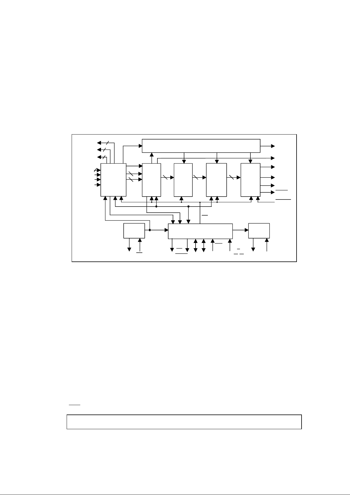
Figure 1. VP305/6 Block Diagram................................................................................................... 7
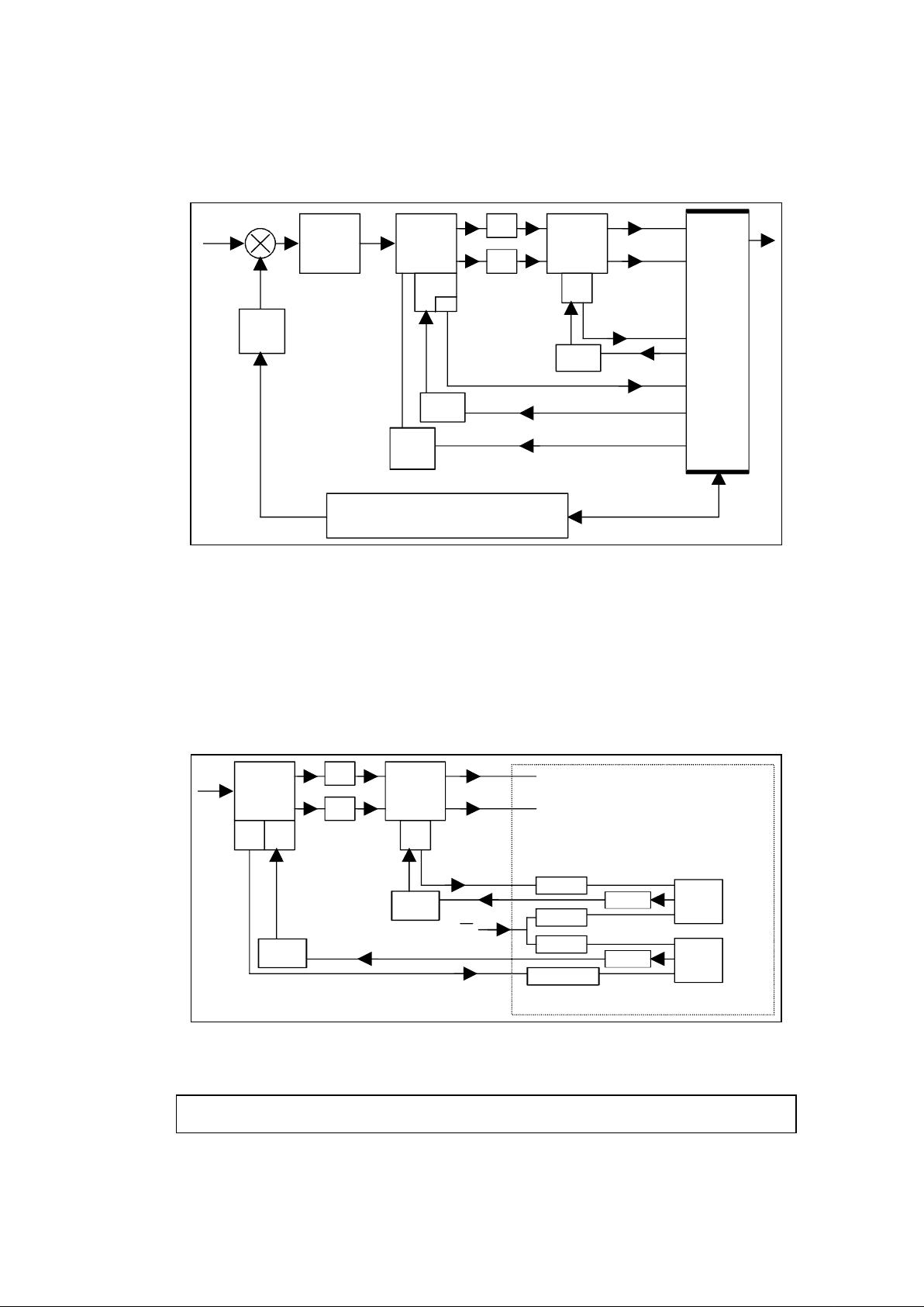
Figure 2. System Application Diagram
.
...........................................................................................9
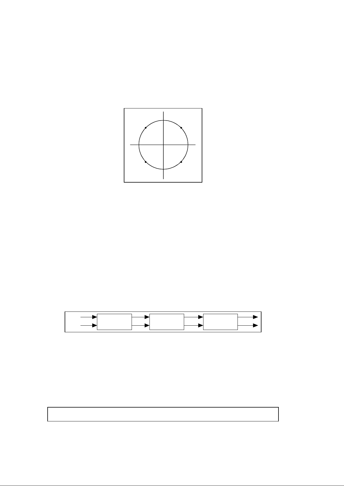
Figure 3. Carrier and Symbol synchronisation diagram.................................................................. 9
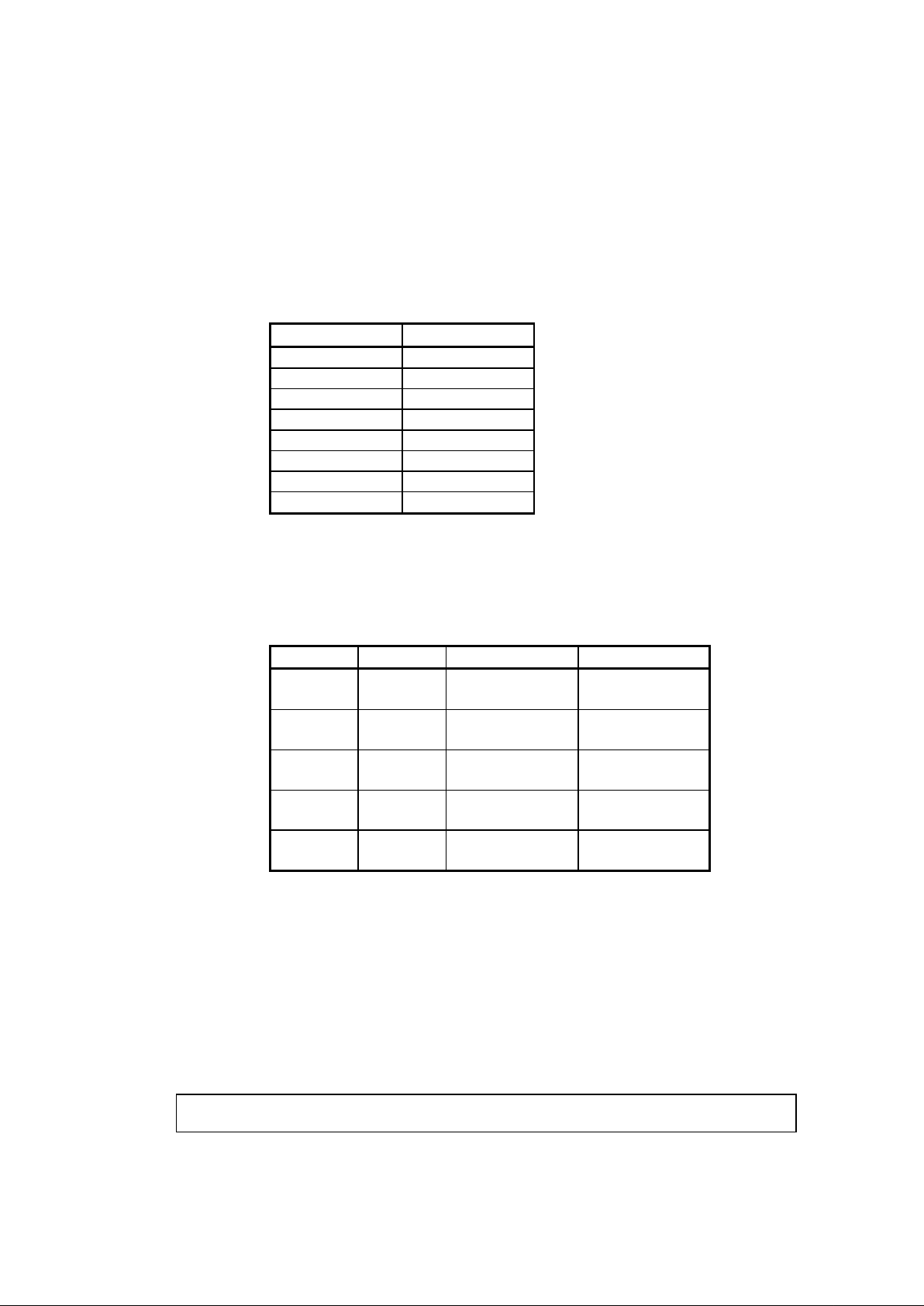
Figure 4. QPSK constellation..........................................................................................................10
Figure 5. Symbol filtering................................................................................................................10
Figure 6. Frequency sweep generator............................................................................................ 11
Figure 7. Viterbi block diagram showing error count generation.....................................................14
Figure 8. Viterbi error count measurement.....................................................................................15
Figure 9. Viterbi error count coarse indication................................................................................16
Figure 10. Conceptual diagram of the convolutional de-interleaver block......................................17
Figure 11. Energy dispersal conceptual diagram............................................................................18
Figure 12. Eye diagram...................................................................................................................34
Figure 13. SNR threshold vs Es / No.............................................................................................36
Figure 14. Carrier sweep rise and fall times vs. CR_OFFSET........................................................38
Figure 15. Carrier phase error detector gain...................................................................................40
Figure 16. Carrier sweep rate for a delta frequency of ±10MHz. .................................................... 43
Figure 17. Parallel interface write cycle action diagram..................................................................61
Figure 18. Parallel interface read cycle action diagram..................................................................63
Figure 19. I²C bus timing.................................................................................................................65
Figure 20. Parallel interface write cycle timing diagram..................................................................66
Figure 21. Parallel interface read cycle timing diagram..................................................................66
Figure 22. VP305/6 data input timing diagram................................................................................67
Figure 23. VP305/6 Transport Packet Header bytes......................................................................68
Figure 24. VP305/6 output data wave form diagram ......................................................................69
Figure 25. VP305/6 data output timing diagram ............................................................................. 70
Figure 26. Crystal oscillator circuit..................................................................................................73
Figure 27. Pin connections - top view.............................................................................................79

VP305/6 DRAFT - PRELIMINARY DATA
The duplication or disclosure of data contained on this sheet is subject to the restrictions
on the title page of this document.
6
LIST OF TABLES.
Table 1. Decimation ratios...............................................................................................................11
Table 2. Viterbi decoder input format..............................................................................................13
Table 3. Viterbi decoder code rate..................................................................................................13
Table 4. De-interleaver data sequence...........................................................................................17
Table 5a. BANK Register................................................................................................................20
Table 5b. Register bank 0. BANK[5:3] = 0 ......................................................................................20
Table 5c. Register bank 1. BANK[5:3] = 8.......................................................................................20
Table 5d. Register bank 2. BANK[5:3] = 16 ....................................................................................21
Table 5e. Register bank 3. BANK[5:3] = 24 ....................................................................................21
Table 5f. Register bank 4. BANK[5:3] = 32 .....................................................................................21
Table 5g. Register bank 5. BANK[5:3] = 40 ....................................................................................22
Table 5h. Register bank 6. BANK[5:3] = 48 ....................................................................................22
Table 5i. Register bank 7. BANK[5:3] = 56......................................................................................22
Table 6a. QPSK Register details.....................................................................................................23
Table 6b. FEC Register details .......................................................................................................24
Table 7. BANK address decodes for parallel mode ........................................................................25
Table 9. Viterbi bit error rate threshold............................................................................................49
Table 10. Number of correct bits in the sync byte..........................................................................50
Table 11. Number of correct sync bytes to retain lock....................................................................50
Table 12. Number of consecutive sync bytes to establish block lock..............................................51
Table 13. Number of incorrect sync bytes to lose lock....................................................................54
Table 14. Enable / disable circuit blocks.........................................................................................56
Table 15. I²C bus timing..................................................................................................................65
Table 16. Parallel bus timing...........................................................................................................67
Table 17. MPEG data output rates..................................................................................................70
Table 18. Recommended operating conditions...............................................................................71
Table 19. DC Characteristics ..........................................................................................................72
Table 20. Pinout details....................................................................................................... ............76
Table 21. Alphabetical listing of the pinout......................................................................................77
Table 22. Numerical listing of the pinout.........................................................................................78
DRAFT - PRELIMINARY DATA VP305/6
The duplication or disclosure of data contained on this sheet is subject to the restrictions
on the title page of this document.
7
PLEASE NOTE:
This manual has the following convention:
All numerical values are shown as decimal numbers, unless otherwise defined.
1. FUNCTIONAL DESCRIPTION.
QPSK
De-inter
leaver
Viterbi
Reed
Solomon
Energy
Dispersal
Test
Microprocessor
Interface
Timing / sync
PSCAL
SYS_CLK
IIN5:0
QIN5:0
3
3
SYMCLK
8 8 8
MDOEN
MDO7:0
XTI
XTO
XTCK
IRQ
DTACK
D7:0
SDA
A2:0
R/W
AS CS
SER
GPP0
RESET
RES
INTQP
INTVI
MCLK
MOSTRT
CR_VCO
AGC_OUT
SYM_VCO
2
2
2
BKERR
GPP4:1
4
VERR
MOVAL
Clock
STATUS
TEST1
TEST2
TEST3
Fig. 1. VP305/6 Block Diagram.
1.1. System overview.
The VP305/6 decoder, together with the SL1710 I/Q down converter and the VP216/7 dual analog
to digital converter (ADC) devices will provide a DVB compliant, satellite receiver system, see
figure 2 on page 9. Before transmission, the data is processed using forward error correction
techniques. Energy dispersal is added to even out 'ones' and 'zeros' for the power handling of the
satellite output transmission devices. The VP305/6 device decodes the signal by reversing all
these encoding techniques.
The VP305/6 contains three phase lock loop systems for control of the voltage controlled
oscillators in the SL1710, the VP216/7 and an internal numerically controlled oscillator (NCO) in
the VP305/6. The NCO can be set to provide a triangular wave form frequency search to establish
symbol lock. There are also two AGC systems in the VP305/6, one controlling the SL1710 gain
and a second internal AGC control of the output power levels from the QPSK block to the Viterbi
block.
A crystal oscillator maintaining circuit is provided to sustain a stable frequency reference clock for
the synthesiser loops. If a crystal is not used, the reference frequency signal may be input on the
XTI
pin.

VP305/6 DRAFT - PRELIMINARY DATA
The duplication or disclosure of data contained on this sheet is subject to the restrictions
on the title page of this document.
8
A system clock (SYS_CLK) running at twice the symbol data rate is provided by the VCO on the
VP216/7 ADC.
The dual ADC circuit digitises the In phase (I) and Quadrature phase (Q) analog signals providing
two, six bit binary offset, data channels. The code range is, from 000000 = least positive valid
output, to 111111 = most positive valid output.
These six bit data channels are input to the VP305/6 on the IIN and QIN pins to the QPSK
demodulator block, see figure 2 on page 9. There the data is decimated and filtered to obtain the
soft decision symbol data to pass to the Viterbi decoder. The QPSK block also generates a bit
clock and resolves the π/2 demodulation phase ambiguity.
The Viterbi decoder recovers the data by a process of de-puncturing, probability analysis and bit
error correction, to obtain the eight bit wide, data bit stream. It also rearranges the bit stream into
bytes, providing a byte clock and packet start signal for the subsequent stages. An indication of
the bit error rate in the data, is provided in the Viterbi block, by comparing the delayed input data
bit stream with the decoded output data bit stream. An actual bit error count may be read from
registers and a coarse indication of the number of errors is provided to facilitate satellite receiver
dish alignment.
The data is then passed to the de-interleaver block where the data is reorganised in a series of
FIFOs into the 204 byte blocks for the Reed Solomon decoder. The de-interleaver depth is 12.
The Reed Solomon decoder is able to correct up to eight byte errors found in the byte data
stream. If there are too many errors to be corrected, the packet will be flagged as uncorrectable.
The 16 check bytes are removed and the 188 byte packet is passed to the next block.
The final data processing block removes Energy Dispersion and inverts the inverted packet
synchronisation byte which is used to mark every eighth 188 byte data packet.
The data output from the VP305/6 is in the form of MPEG2 transport stream data packets on the
MDO7:0 data bus, together with clock, data start, data valid and block error signals. The data rate
is automatically varied, according to the puncture rate, to reduce the instantaneous data rate and
the inter packet period.
DRAFT - PRELIMINARY DATA VP305/6
The duplication or disclosure of data contained on this sheet is subject to the restrictions
on the title page of this document.
9
VCO
LPF
LPF
SL1710
I/Q DOWN
CONVERT
VP216/7
DUAL ADC
IIN
QIN
SYS_CLK
VCO
LOOP
FILTER
LOOP
FILTER
479.5MHz
PSCAL
CR_VCO
SYM_VCO
VP305/6
14.984375MHz
AGC
LOOP
FILTER
SAW
SP5658
FREQ
SYNTH.
FROM
LNB
MICROPROCESSOR
AGC_OUT
/32
Fig. 2. System Application Diagram.
1.2. The QPSK Demodulator block.
The QPSK demodulator block performs the function of locking the receiver system to the incoming
data stream. It controls the voltage controlled oscillators (VCO) in the SL1710 I/Q down converter
and the VP216/7 dual analog to digital converter (ADC). The carrier frequency VCO is locked to
maintain the intermediate frequency (IF) of 479.5MHz. The symbol frequency VCO synthesiser
loop is locked to the twice the required symbol frequency (in the zero decimation case) and
generates the system clock SYS_CLK which is running at the bit rate.
/32 VCO
LPF
LPF
SYM_RP
SL1710
I/Q DOWN
CONVERT
VP216/7
DUAL ADC
IIN
QIN
SYS_CLK
XTI
VCO
LOOP
FILTER
LOOP
FILTER
479.5MHz
PSCAL
CR_VCO
SYM_VCO
VP305/6
14.984375MHz
CR_RP
SYM_NF
AFC
CR_U/LSWL
CONV
CONV
VCO
SWEEP
GEN
Fig. 3. Carrier and Symbol frequency synthesiser diagram.
VP305/6 DRAFT - PRELIMINARY DATA
The duplication or disclosure of data contained on this sheet is subject to the restrictions
on the title page of this document.
10
1.2.1. Input requirements.
The data input is digitised six bit I and Q channel data in the form of either binary format or offset
2's complement data. The QPSK phase constellation representation is shown below.
I = 0
Q = 1
I = 0
Q = 0
I = 1
Q = 0
I = 1
Q = 1
I
Q
Fig. 4. QPSK constellation.
1.2.3. Matched filters
The Decimation filter and matched filter together have a 0.35 roll-off square-root-raised-cosine
frequency response as in reference 1.
1.2.4. Decimation filters
In order to adjust to the wide range of symbol rates (5 to 30Msym/s), the I and Q data in may be
decimated by varying degrees. The system also allows for the ADC sample clock to be adjusted to
within the range 30 to 62MHz.
The sample rate at the input to the matched filter is equal to twice the symbol rate, 2Rs. The
SYM_DR bits in the SYM_CONFIG register can be programmed to allow for the following filtered
symbol rates at the input to the VP305/6:
2Rs, 3Rs, 4Rs, where Rs = symbol rate.
SYM_RATIO
unfiltered
Decimation
Matched
Filter
SYM_RP
filtered
Decimation
IIN
QIN
Fig. 5. Symbol filtering.
The SYM_RATIO register allows the input symbol rate to be extended further to cover 6Rs, 8Rs,
12Rs, 16Rs, 24Rs, 32Rs, 48Rs and 64Rs unfiltered decimation rates.
The number of samples / Symbol (M) can be calculated from the formula:
M = (SYM_DR over sample rate) * (2
SYM_RATIO
)
The range of values of M is shown in the table below.

DRAFT - PRELIMINARY DATA VP305/6
The duplication or disclosure of data contained on this sheet is subject to the restrictions
on the title page of this document.
11
SYM_RATIO01234
SYM_DR M
samples/SymMsamples/SymMsamples/SymMsamples/SymMsamples/Sym
0 - (over sample 2) 2 4 8 16 32
1 - (over sample 4) 4 8 16 32 64
2 - (over sample 3) 3 6 12 24 48
Table 1. Decimation ratios.
1.2.5. Carrier frequency synchronisation
The SL1710 local oscillator frequency of 479.5MHz is maintained by a frequency synthesis loop
on the VP305/6. The SL1710 voltage controlled oscillator (VCO) frequency is divided internally by
32 to generate a push-pull feedback reference frequency signal. This is connected to the VP305/6
PSCAL PECL inputs and then to the CR_U/LSWL dividers. The output from the CR_U/LSWL
dividers is compared with the crystal oscillator frequency divided by the CR_RP division ratio. A
feedback signal (CR_VCO) is output to an active filter to complete the loop and control the
SL1710 VCO, see Fig. 3 on page 9.
The internal frequency sweep generator is controlled by the CR_SWR, CR_USWL,CR_LSWL,
CR_RP registers and turned on and off by the CR_SW bit in the CONFIG register. The diagram in
Fig. 3 on page 9 shows the registers which set up the dividers for both the carrier and symbol
phase locked loops.
f
t
Upper
Sweep
Limit
Lower
Sweep
Limit
Sweep
Start
Point
Fig. 6. Frequency sweep generator.
The carrier frequency reference period (CR_RP register) sets the count of the crystal clock cycles
(XTI
pin). This sets the reference for the measurement of the I/Q down converter VCO frequency
(PSCAL pins). The register value sets the 4 most significant bits of a 14 bit counter. The actual
count is CR_RP[3:0] * 1024.

VP305/6 DRAFT - PRELIMINARY DATA
The duplication or disclosure of data contained on this sheet is subject to the restrictions
on the title page of this document.
12
The comparison frequency, Fcomp =
Fcrystal
CR_RP * 1024
MHz.
The upper and lower sweep boundaries are set by the CR_USWL and CR_LSWL respectively.
These registers actually set the division ratios for dividing the I/Q down converter VCO frequency.
The value programmed must take account of any fixed prescaler in the I/Q down converter, for the
SL1710 this is divide by 32.
The comparison frequency, Fcomp =
Fvco
32 * CR_U/LSWL
MHz.
Therefore,
Fcrystal
CR_RP * 1024
=
Fvco
32 * CR_U/LSWL
Therefore, Fcrystal * 32 * CR_U/LSWL = Fvco * CR_RP * 1024
Therefore,
Fvco
Fcrystal
=
32 * CR_U/LSWL
CR_RP * 1024
The upper and lower sweep limits can be expressed in terms of the above equations together with
two further terms including the delta variation in frequency.
Let the delta variation in frequency = ± δF.
Then the frequency limits are Fvco + δF and Fvco - δF.
Therefore, CR_USWL =
(Fvco + δF) * CR_RP * 1024
Fcrystal * 32
and CR_LSWL =
(Fvco - δF) * CR_RP * 1024
Fcrystal * 32
When the AFC circuit achieves lock, as indicated by the CR_FLOCK bit in the STATUS register
going high, the scaled carrier frequency can be read from the CR_VCOF U & L registers.
The actual carrier frequency is found from the following formula:
Fvco =
32 * Fcrystal
CR_RP * 1024
* CR_VCOF MHz see page 30.
1.2.6. Symbol synchronisation and tracking
The VP216/7 local oscillator frequency must be programmed to be at least twice the required
symbol rate and is maintained by a Phase Locked Loop on the VP305/6. The ADC sample
frequency should be adjusted by setting the SYM_NF and SYM_RP division ratios to match the
decimation rate chosen. The VP216/7 voltage controlled oscillator (VCO) frequency is connected
to the VP305/6 SYS_CLK input and then to the SYM_NF divider. The output from the SYM_NF
divider is compared with the crystal oscillator frequency divided by the SYM_RP division ratio. A
push-pull feedback signal (SYM_VCO) is output to an active filter to complete the loop and control
the VP216/7 VCO, see Fig. 3 on page 9.
DRAFT - PRELIMINARY DATA VP305/6
The duplication or disclosure of data contained on this sheet is subject to the restrictions
on the title page of this document.
13
1.3. The Viterbi Decoder block.
The Viterbi decoder input data format uses three bit, two's complement coding representation of
the data in the following form, (binary numbers):
I or Q value Interpretation
011 most likely one
010
001
000 least likely one
111 least likely zero
110
101
100 most likely zero
Table 2. Viterbi decoder input format.
The first task for the Viterbi decoder is to 'de-puncture' the data. This is a process of restoring data
bits which have been removed (punctured), prior to transmission, to improve the transmission
efficiency. The de-puncture code rate must be programmed into the VIT MODE register. The
following patterns are used:
VITCR[2:0] Code rate Input bit stream Output bit stream
0 1/2 I = X
1
Q = Y
1
X = 1
Y = 1
1 2/3 I = X1Y2Y
3
Q = Y1X3Y
4
X = 1010
Y = 1111
2 3/4 I = X1Y
2
Q = Y1X
3
X = 101
Y = 110
3 5/6 I = X1Y2Y
4
Q = Y1X3X
5
X = 10101
Y = 11010
4 7/8 I = X1Y2Y4Y
6
Q = Y1Y3X5X
7
X = 1000101
Y = 1111010
Table 3. Viterbi decoder code rate.
The zeros in the above table represent unknown data bit values, effectively error bits. The decoder
uses a trace back trellis technique to remove the uncertainty and recover the correct data. The
trace back depth is 128.
VP305/6 DRAFT - PRELIMINARY DATA
The duplication or disclosure of data contained on this sheet is subject to the restrictions
on the title page of this document.
14
1.3.1. Viterbi error count measurement.
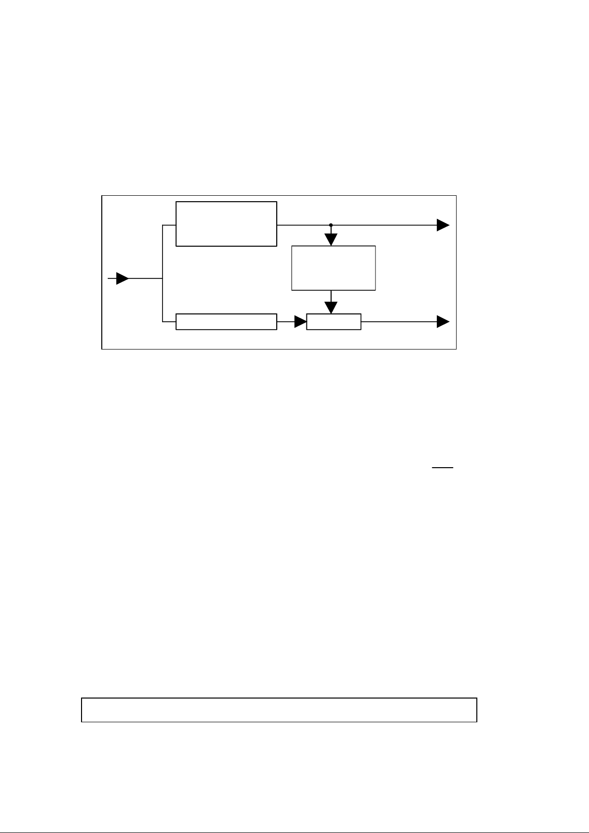
A measure of the effectiveness of the Viterbi decoder in removing bit errors is provided in the
VP305/6. The incoming data bit stream is delayed and compared with the decoded bit stream to
obtain a count of errors corrected by the decoder, see the Fig. 7 below.
VITERBI
DECODER
DELAY COMP
ERROR COUNT
DATA BIT STREAM
VITERBI
ENCODER
Fig. 7. Viterbi block diagram showing error count generation.
The measurement system has a programmable register to determine the number of data bits (the
error count period) over which the count is being recorded. A read register indicates the error
count result and an interrupt can be generated to inform the host microprocessor that a new count
is available.
The VIT ERR H-M-L group of three registers is programmed with required number of data bits (the
error count period) (VITEP[23:0]). The actual value is four times VITEP[23:0]. The count of errors
found during this period is loaded by the VP305/6 into the VIT ERR C H-L pair of registers when
the bit count VITEP[23:0] is reached. At the same time an interrupt is generated on the IRQ
line.
The actual error count value is four times VERRC[15:0]. If a value of 65535 is read out, the error
count is too large for the VERRC[15:0] registers, so the error period in VITEP[23:0] should be
reduced. The interrupt is enabled by setting the IE_FEC[2] bit in the IE_FEC register, see
page 52. VERRC[15:0] is not cleared by reading the register, it is only loaded with the error count.
DRAFT - PRELIMINARY DATA VP305/6
The duplication or disclosure of data contained on this sheet is subject to the restrictions
on the title page of this document.
15
VITEP[23:0]
DATA BITS
ERROR
COUNT
VERRC[15:0]
0
0
IRQ
Fig. 8. Viterbi error count measurement.
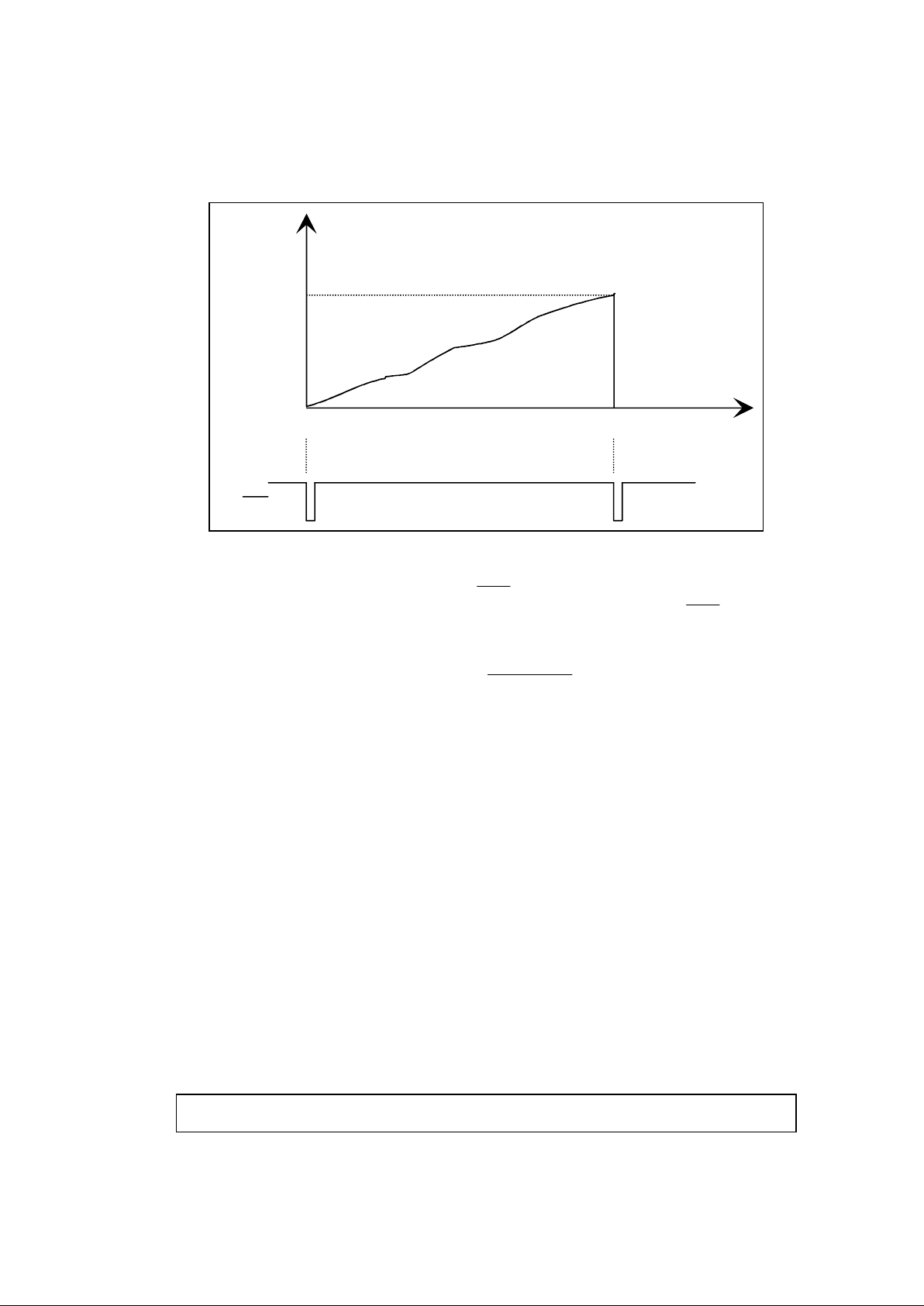
Figure 8 above shows the bit errors rising until the maximum programmed value of VITEP[23:0] is
reached, when an interrupt is generated on the IRQ
line to advise the host microprocessor that a
new value of bit error count has been loaded into the VERRC[15:0] register. The IRQ
line will go
high when the IE_FEC register is read by the host microprocessor.
The error count may be expressed as a ratio:
VERRC[15:0]
VITEP[23:0]
.
1.3.2. Viterbi error count coarse indication.
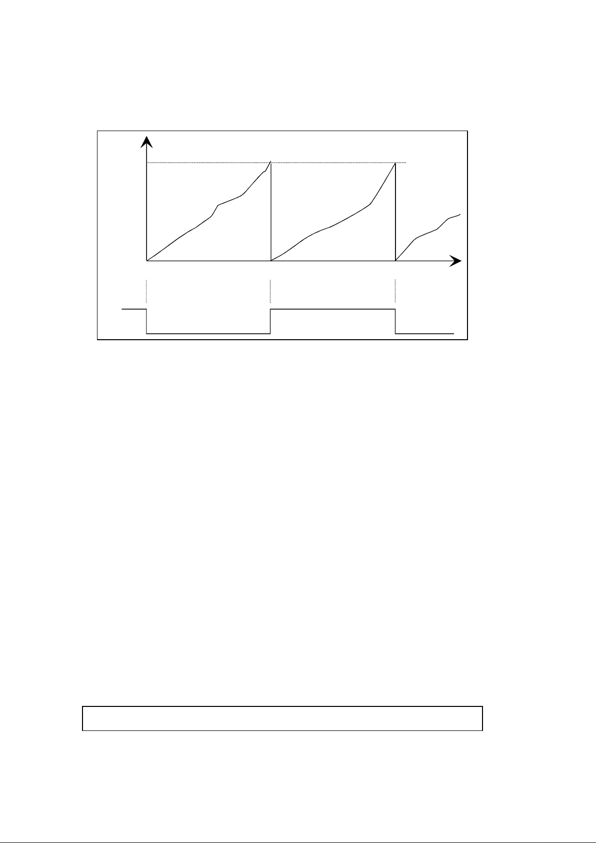
To assist in the process of aligning the receiver dish aerial, a coarse indication of the number of bit
errors being received can be provided by monitoring the VERR line with the following set up
conditions.
The frequency of the output wave form will be a function of the bit error count (triggering the
maximum value programmed into the VI MAX ERR register (VMERR[7:0])) and the dish alignment
on the satellite. This VERR mode is enabled by setting the INTVIS bit in the TEST2 register.
Figure 9 below shows the bit errors rising to the maximum programmed value and triggering a
change of state on the VERR line.
VP305/6 DRAFT - PRELIMINARY DATA
The duplication or disclosure of data contained on this sheet is subject to the restrictions
on the title page of this document.
16
DAT A BITS
VITERBI
COARS E
BIT
ERROR
COUNT
VME RR[7:0]
0
0
VE R R
Fig. 9. Viterbi error count coarse indication.
1.4. The De-interleaver block.
Before transmission, the data bytes are interleaved with each other in a cyclic pattern of twelve.
This ensures the bytes are spaced out, so that successive message bytes are transmitted with a
separation of at least 12 bytes. This system is used to avoid the possibility of a noise spike
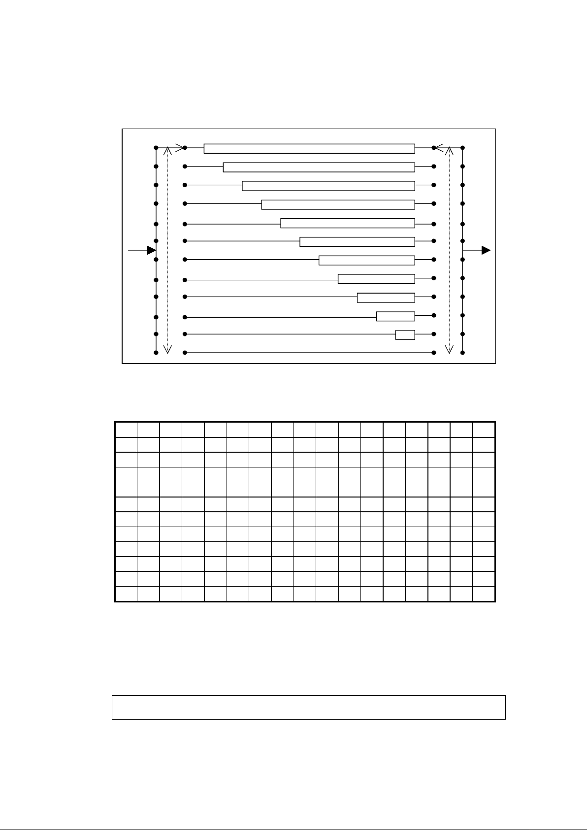
corrupting a group of consecutive message bytes. The diagram below shows conceptually how
the convolutional de-interleaving system works. The synchronisation byte is always loaded into the
First-In-First-Out (FIFO) memory in branch 0. The switch is operated at regular byte intervals to
write successively received bytes into the next branch. After 12 bytes have been received, byte 13
is written next to the synchronisation byte in branch 0, etc. Only when the FIFOs are full, will the
read out of the 204 byte message be enabled. On the VP305/6, this function is realised in random
access memory (RAM) with some spare capacity to avoid messages being over written before
they are read out.
DRAFT - PRELIMINARY DATA VP305/6
The duplication or disclosure of data contained on this sheet is subject to the restrictions
on the title page of this document.
17
0
1
2
3
4
5
6
7
8
9
10
11
0
1
2
3
4
5
6
7
8
9
10
11
Sync word route
17x1
17x2 bytes
17x3 bytes
17x4 bytes
17x5 bytes
17x6 bytes
17x7 bytes
17x8 bytes
17x9 bytes
17x10 bytes
17x11 bytes
one
byte per
position
Fig. 10. Conceptual diagram of the convolutional de-interleaver block.
The byte sequence for the first 204 byte block is shown below. Each row represents one branch
FIFO.
1 13 25 37 49 61 73 85 97 109 121 133 145 157 169 181 193
2 14 26 38 50 62 74 86 98 110 122 134 146 158 170 182 194
3 15 27 39 51 63 75 87 99 111 123 135 147 159 171 183 195
4 16 28 40 52 64 76 88 100 112 124 136 148 160 172 184 196
5 17 29 41 53 65 77 89 101 113 125 137 149 161 173 185 197
6 18 30 42 54 66 78 90 102 114 126 138 150 162 174 186 198
7 19 31 43 55 67 79 91 103 115 127 139 151 163 175 187 199
8 20 32 44 56 68 80 92 104 116 128 140 152 164 176 188 200
9 21 33 45 57 69 81 93 105 117 129 141 153 165 177 189 201
10 22 34 46 58 70 82 94 106 118 130 142 154 166 178 190 202
11 23 35 47 59 71 83 95 107 119 131 143 155 167 179 191 203
12 24 36 48 60 72 84 96 108 120 132 144 156 168 180 192 204
Table 4. De-interleaver data sequence.
VP305/6 DRAFT - PRELIMINARY DATA
The duplication or disclosure of data contained on this sheet is subject to the restrictions
on the title page of this document.
18
1.5. The Reed Solomon block.
In the Transmission system, the MPEG2 message packet is encoded using the Reed Solomon
RS(204,188, T=8) shortened code. This converts the 188 byte data packet into a Reed Solomon
encoded block containing 204 bytes. The 16 check bytes allow the decoding system to search the
packet for errors and correct up to eight bytes containing errors. If there are more than eight bytes
containing errors, the packet is flagged as containing uncorrectable errors by pulling the BKERR
pin low and setting the TEI bit in the second byte of the packet header, see figure 21 on page 68.
The number of blocks containing uncorrectable errors may be read from the RS UBC register
which is reset to zero each time it is read. The 16 check bytes are discarded before the data
packet is passed on to the Energy Dispersal block.
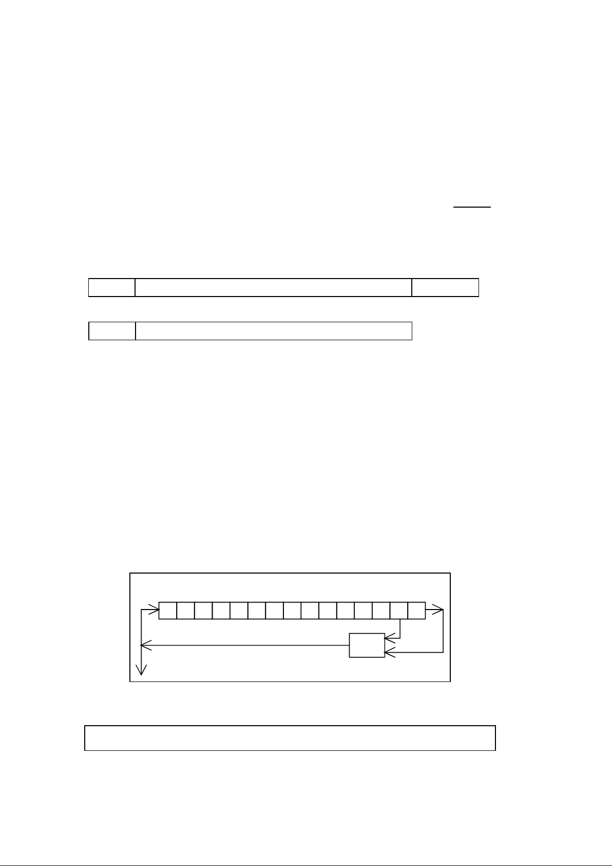
Sync byte 187 bytes 16 check bytes
Reed Solomon encoded block.
Sync byte 187 bytes
MPEG2 transport packet.
1.6. The Energy Dispersal (descrambler) block.
Before Reed Solomon encoding in the transmission system, the MPEG2 data stream is
randomised using the configuration shown in figure 11 below. This is a Pseudo Random Binary
Sequence (PRBS) generator, with the polynomial:
1 + X
14
+ X
15
The PRBS registers are loaded with the initialisation sequence as shown, at the start of the first
transport packet in a group of eight packets. This point is indicated by the inverted sync byte
B8
hex
. The normal sync. byte is 47
hex
. The data starting with the first byte after the sync. byte is
randomised. (The sync. bytes themselves are not randomised).
In the decoder, the process of de-randomising or de scrambling the data is exactly the same as
described above.
123456789101112131415
100101010000000
Initialisation sequence
XOR
Fig. 11. Energy dispersal conceptual diagram
.

DRAFT - PRELIMINARY DATA VP305/6
The duplication or disclosure of data contained on this sheet is subject to the restrictions
on the title page of this document.
19
1.6.1. Output stage.
A complete transport stream data packet of 188 bytes is output on the MDO7:0 bus, clocked by
the MCLK signal. The MDO7:0 bus is enabled by pulling the MDOEN
low. The start sync byte is
flagged by the MOSTRT signal going high and the MOVAL signal will also go high to indicate a
valid packet. If the packet contains uncorrectable bytes, a BKERR
signal will go low on the first
error byte and remain low until the end of the packet. The TEI bit in the packet header can
optionally be set automatically to indicate a packet with uncorrectable bytes.
1.7. Microprocessor interface.
This interface can be either a serial I²C bus or a parallel interface port, see section 3 starting on
page 58.
VP305/6 DRAFT - PRELIMINARY DATA
The duplication or disclosure of data contained on this sheet is subject to the restrictions
on the title page of this document.
20
2. REGISTER DETAILS
2.1. Parallel interface register map.
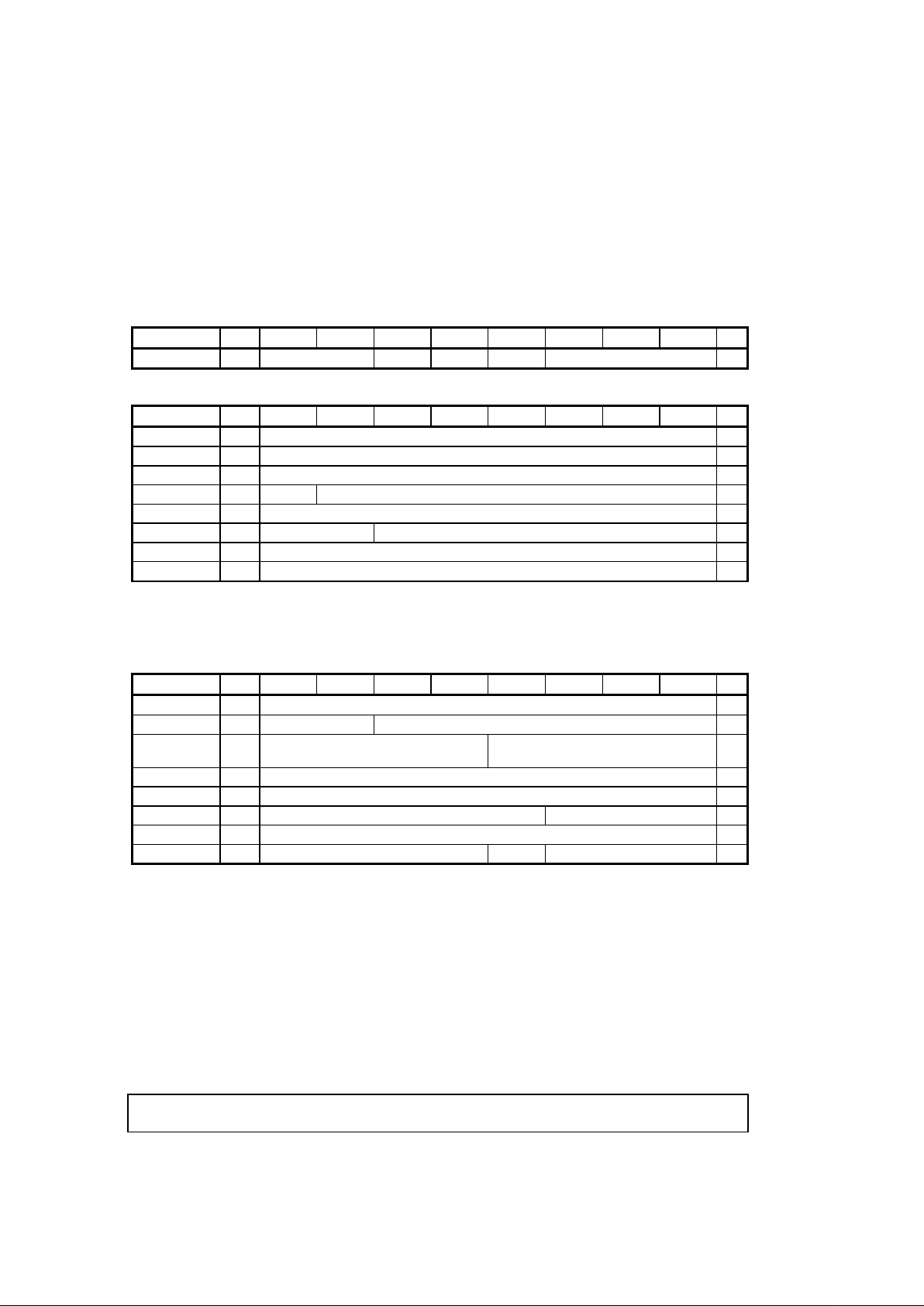
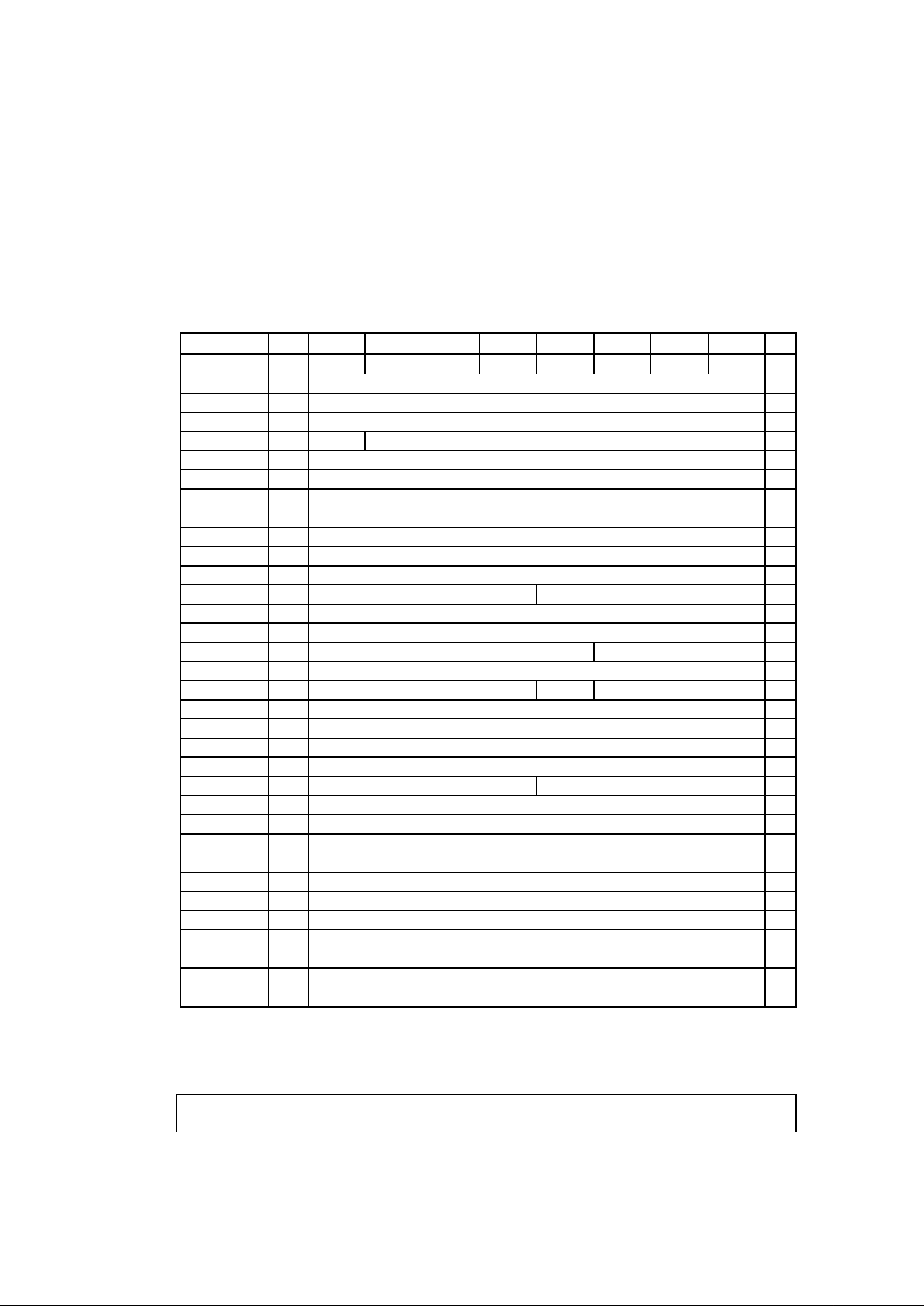
The default state of almost all of the registers is zero, except the ID register and unused registers.
Reserved or unused bits should be set to zero when writing to a register.
NAMEADRD7D6D5D4D3D2D1D0R/W
BANK 0 Reserved AD5 AD4 AD3 Reserved W
Table 5a. BANK Register 0. (Address byte = 0, Data byte = NEXT BANK
)
NAMEADRD7D6D5D4D3D2D1D0R/W
ID 0 ID[7:0] Chip identifi cation R
INT_QPSK 1 INT_QPSK[7:0] Interrupt QPSK R
INT_FEC 2 INT_FEC[7:0] Interrupt FEC R
STATUS 3 Reserved STATUS[6:0] R
AGC_LVL 4 AGC_LVL[7:0] AGC loop volt age meter R
CR_VCOF U 5 Res erved CR_VCOF[13:8] Measured VCO frequency (upper nibble) R
CR_VCOF L 6 CR_VCOF[7:0] Measured VCO frequency (lower byte) R
IE_QPSK 7 IE_QPSK[7:0] Interrupt enable QPSK R/W
Table 5b. Register bank 0. BANK[5:3] = 0.
Note: In Bank 0, the registers 1 to 6 are READ only. Writing to these addresses will have no
effect.
NAMEADRD7D6D5D4D3D2D1D0R/W
ID 0 ID[7:0] Chip identifi cation R
SYM_CONFIG 1 Reserved SYM_CONFIG[5:0] Symbol configuration R/W
SYM_RP 2 Reserved SYM_RP[3:0] Symbol A FC reference
period
R/W
SYM_NF U 3 SYM_NF[15:8] Symbol input nominal frequency (upper byte) R/W
SYM_NF L 4 SYM_NF[7:0] Symbol input nominal frequency (lower byte) R/W
SYM_RATIO 5 Reserved SYM_RATIO[2:0] R/W
AGC_REF 6 AGC_REF[7:0] Referenc e AGC level R/W
AGC_BW 7 Reserved INT_DC AGC_BW[2: 0] R/W
Table 5c. Register bank 1. BANK[5:3] = 8.
DRAFT - PRELIMINARY DATA VP305/6
The duplication or disclosure of data contained on this sheet is subject to the restrictions
on the title page of this document.
21
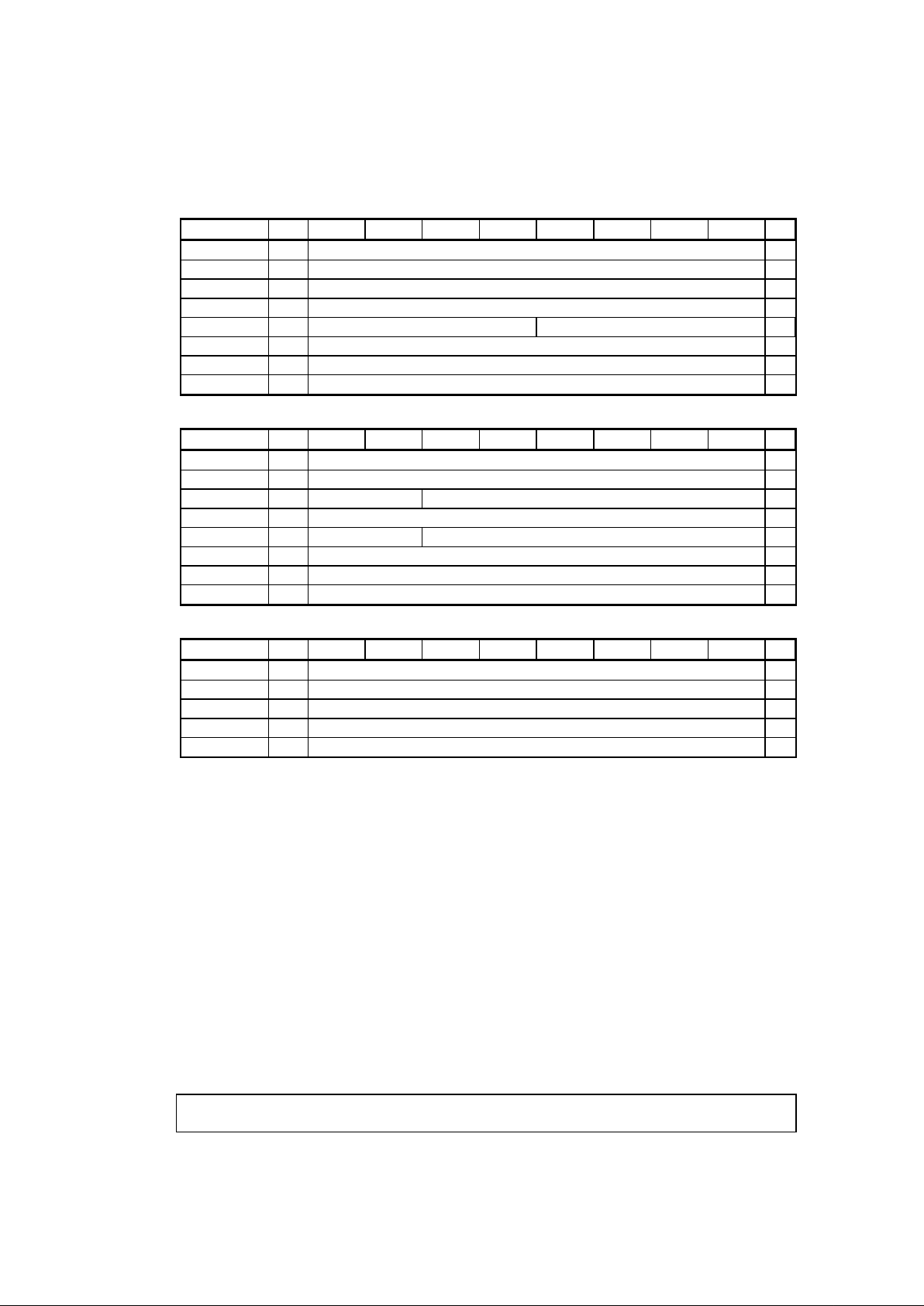
NAMEADRD7D6D5D4D3D2D1D0R/W
ID 0 ID[7:0] Chip identifi cation R
SCALE 1 SCALE[7:0] Scale factor for IOUT and QOUT outputs R/W
SNR_THS 2 SNR_THS[7:0] SNR estimator threshold R/W
CR_OFFSET 3 CR_OFFSET[7:0] Carrier loop DC offset compensation value R/W
CR_RP 4 Reserved CR_RP[3:0] Carrier reference peri od R/W
CR_KP 5 CR_KP[7:0] Carri er l oop filter gain (P term) R/W
CR_KD 6 CR_KD[7:0] Carrier loop filter gain (D term) R/W
CR_THSL 7 CR_THSL[7:0] Carrier lock detector threshold R/W
Table 5d Register bank 2. BANK[5:3] = 16.
NAMEADRD7D6D5D4D3D2D1D0R/W
ID 0 ID[7:0] Chip identifi cation R
CR_SWR 1 CR_SWR[7:0] Carrier sweep rate R/W
CR_USWL U 2 Reserved CR_USWL[13:8] Carri er Upper sweep limit (upper nibble) R/W
CR_USWL L 3 CR_USWL[7:0] Carrier Upper sweep limi t (lower byte) R/W
CR_LSWL U 4 Reserved CR_LSW L[13:8] Carrier Lower sweep limit (upper nibbl e) R/ W
CR_LSWL L 5 CR_LSWL[7: 0] Carri er Lower sweep limit (lower byte) R/ W
CR_CONFIG 6 CR_CONFIG[7:0] Carrier conf i gurat i o n R/W
CONFIG 7 CONFIG[7:0] Configuration R/W
Table 5e. Register bank 3. BANK[5:3] = 24.
NAMEADRD7D6D5D4D3D2D1D0R/W
ID 0 ID[7:0] Chip identifi cation R
VIT_ERR_C H 1 VERRC[15:8] - Viterbi error count high byte R
VIT_ERR_C L 2 VERRC[7:0] - V i terbi error count low byte R
RS_UBC 3 RSUBC[7:0] - Reed Solomon uncorrect ed bl ock count R
Not used 4 - 7 Writing to these addresses will have no effect. Reading will return 255 R/W
Table 5f. Register bank 4. BANK[5:3] = 32.
Note: In Bank 4, the registers 1 to 3 are READ only and registers 4 to 7 are not used. Writing to
these addresses will have no effect.
VP305/6 DRAFT - PRELIMINARY DATA
The duplication or disclosure of data contained on this sheet is subject to the restrictions
on the title page of this document.
22
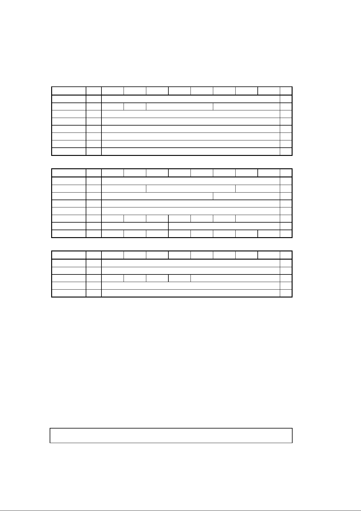
NAMEADRD7D6D5D4D3D2D1D0R/W
ID 0 ID[7:0] Chip identifi cation R
VIT_MODE 1 IQSWAP F_LOCK Reserved VITCR[2:0] - code rate R/W
VIT_ERR H 2 VITEP[23:16] - Viterbi error period high byte R/W
VIT_ERR M 3 VITEP[15:8] - V i terbi error period middle byte R/W
VIT_ERR L 4 VITEP[7:0] - Viterbi error peri od l ow byte R/W
VI_MAX_ERR 5 VMERR[7:0] - Viterbi max. bit error count R/W
VI_BER_PER 6 VBPER[7:0] - Viterbi bit error rate based synchronisation period R/W
VI_BER_LIM 7 VBLIM[7:0] - Viterbi bit error rate based synchronisation limi t R/W
Table 5g. Register bank 5. BANK[5:3] = 40.
NAMEADRD7D6D5D4D3D2D1D0R/W
ID 0 ID[7:0] Chip identifi cation R
VIT_CTRL1 1 BS_MODE[1:0] VS_UNLK[3:0] VBIT_MV[1:0] R/W
VIT_CTRL2 2 Reserved VS_LK[2:0] R/W
IE_FEC 3 IE_FEC[7:0] Interrupt enable FEC R/W
STAT_EN 4 STA T_EN[7:0] Enable various output s on STATUS pin. R/W
GEN_CTRL 5 - - - MCLKINV BSO ENTEI NSYNC[1:0] R/ W
GPP_CTRL 6 Reserved GPP_CTRL[4:0] R/W
RESET 7 RES - - - PR_DS PR_BS FR_QP PR_QP R/W
Table 5h. Register bank 6. BANK[5:3] = 48
.
NAMEADRD7D6D5D4D3D2D1D0R/W
ID 0 ID[7:0] Chip identifi cation R
TEST1 1 Reserved R/W
TEST2 2 INTVIS - - - EN[3:0] R/W
TEST3 3 Reserved R/W
Not used 4 - 7 Writing to these addresses will have no effect. Reading will return 255 R/W
Table 5i. Register bank 7. BANK[5:3] = 56
.
Note: In Bank 7, the registers 4 - 7 are not used. Writing to these addresses will have no effect.
Note: When writing to, or reading from registers which are part of a group, all registers in the
group must be addressed for the data transfer to be sucessfully completed.
DRAFT - PRELIMINARY DATA VP305/6
The duplication or disclosure of data contained on this sheet is subject to the restrictions
on the title page of this document.
23
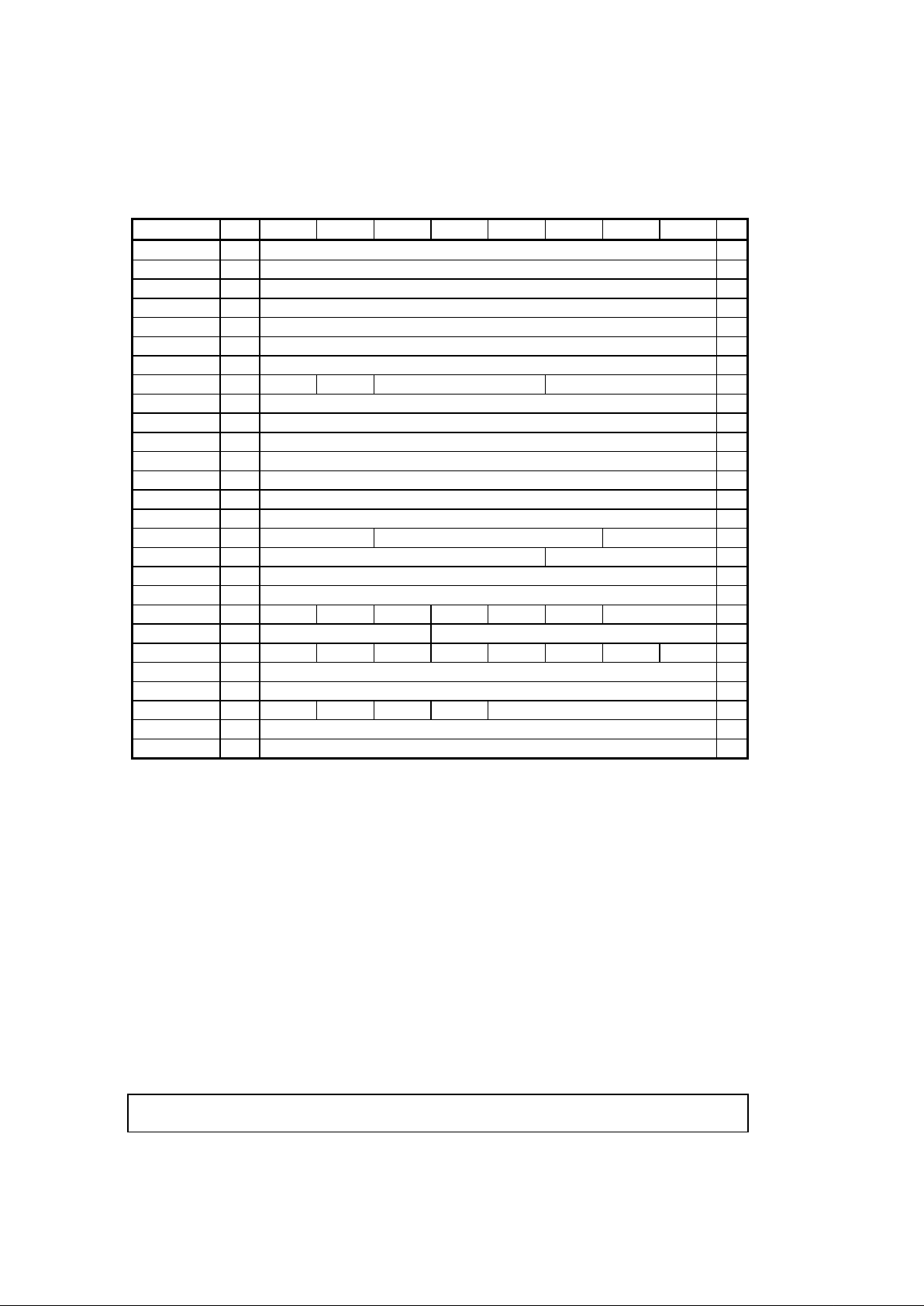
2.2. Serial interface register map.
Not available on VP305.
The default state of all registers is reset to 0.
Reserved or unused bits should be set to zero when writing to a register.
All values are shown as decimal numbers, unless otherwise defined.
NAMEADRD7D6D5D4D3D2D1D0R/W
RADD IAI AD6 AD5 AD4 AD3 AD2 AD1 AD0 W
ID 00 ID[7:0] Chip identification. Writing to this address will have no effect. R
INT_QPSK 01 INT_QPSK[7:0] Interrupt QPSK R
INT_FEC 02 INT_FEC[7:0] Interrupt FEC R
STATUS 03 Reserved STATUS[6:0] R
AGC_LVL 04 AGC_LV L[ 7:0] AGC loop voltage meter R
CR_VCOF U 05 Reserved CR_VCOF[13:8] Measured VCO frequency (upper nibble) R
CR_VCOF L 06 CR_VCOF[7:0] Measured V CO f requency (lower byte) R
Not used 01-06 Writing to these addres s es will have no effect. W
IE_QPSK 07 IE_QPSK[7:0] Interrupt enable QPSK R/W
ID 08 ID[7:0] Chip identification. Writing to this address will have no effect. R
SYM_CONFIG 09 Reserved SYM_CONFIG[5:0] Symbol configuration R/W
SYM_RP 10 Reserved SYM_RP[3:0] Symbol AFC ref. peri od R/W
SYM_NF U 11 S YM_NF[15:8] Symbol input nominal frequency (upper byte) R/W
SYM_NF L 12 SYM_NF[7:0] Symbol input nominal f requency (lower byte) R/W
SYM_RATIO 13 Reserved SYM_RATIO[2:0] R/W
AGC_REF 14 AGC_REF[7:0] Reference AGC level R/W
AGC_BW 15 Reserved INT_DC AGC_BW[2:0] R/W
ID 16 ID[7:0] Chip identification. Writing to this address will have no effect. R
SCALE 17 SCA LE[7:0] Scale fact or for IOUT and QOUT outputs R/W
SNR_THS 18 SNR_THS[7:0] S NR estimator threshol d R/W
CR_OFFSET 19 CR_OFFSET[7:0] Carrier loop DC offset compensation value R/W
CR_RP 20 Reserved CR_RP[3:0] Carrier reference period R/W
CR_KP 21 CR_KP[7:0] Carrier loop fil ter gain (P term) R/W
CR_KD 22 CR_KD[7:0] Carrier loop filter gain (D term) R/W
CR_THSL 23 CR_THSL[7:0] Carrier lock detector threshold R/W
ID 24 ID[7:0] Chip identification. Writing to this address will have no effect. R
CR_SWR 25 CR_SWR[7:0] Carrier sweep rate R/W
CR_USWL U 26 Reserved CR_USWL[13:8] Carrier Upper sweep limi t (upper nibble) R/W
CR_USWL L 27 CR_US WL[7:0] Carrier Upper sweep limit (lower byte) R/W
CR_LSWL U 28 Res erved CR_LSWL[13:8] Carrier Lower sweep limit (upper nibble) R/W
CR_LSWL L 29 CR_LSWL[7:0] Carrier Lower sweep limit (lower byte) R/W
CR_CONFIG 30 CR_CONFIG[ 7 : 0 ] Carrier configuration R/W
CONFIG 31 CONFIG[7:0] Configuration R/W
Table 6a. QPSK Register details.
VP305/6 DRAFT - PRELIMINARY DATA
The duplication or disclosure of data contained on this sheet is subject to the restrictions
on the title page of this document.
24
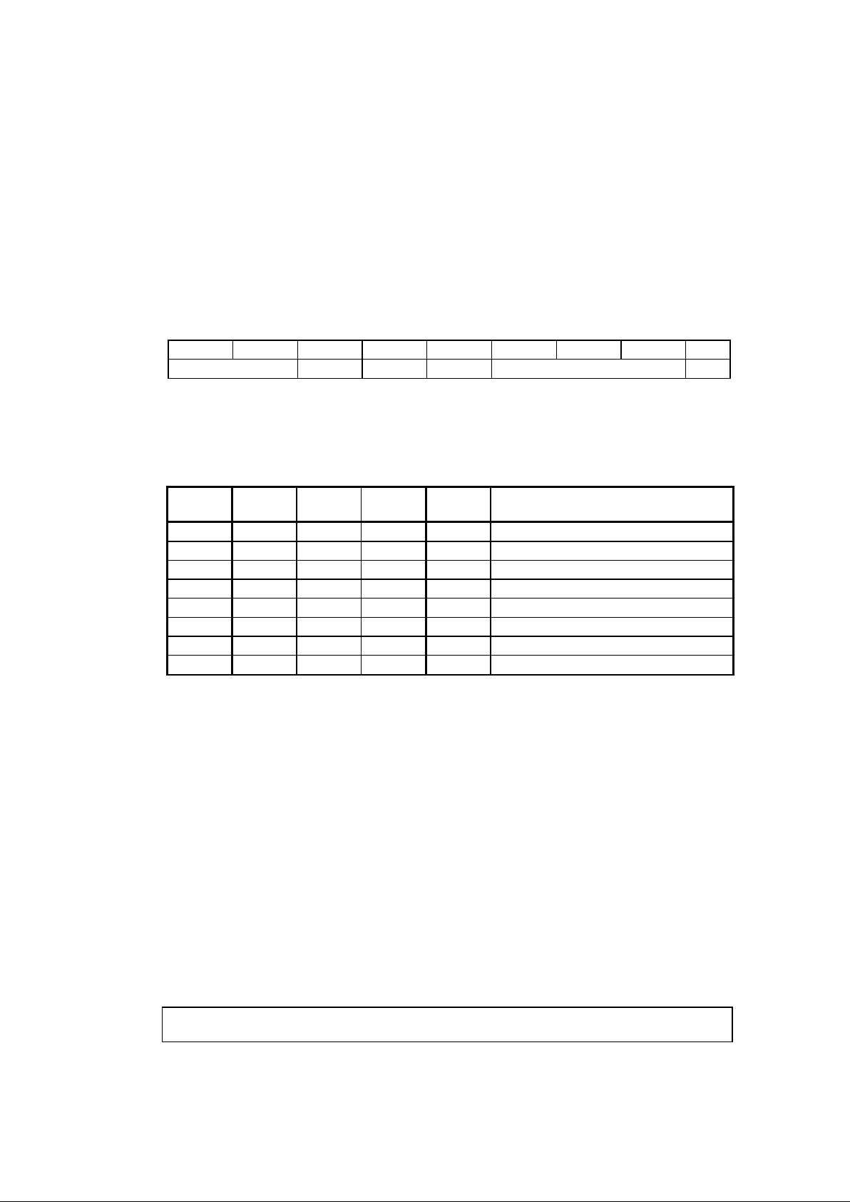
NAMEADRD7D6D5D4D3D2D1D0R/W
ID 32 ID[7:0] Chip identification. Writing to this address will have no effect. R
VIT_ERR_C H 33 VERRC[15:8] - Vi terbi error count high byte R
VIT_ERR_C L 34 VERRC[7:0] - V iterbi error count low byte R
RS_UBC 35 RSUBC[7:0] - Reed Solomon uncorrected bloc k count R
Not used 33-35 Writing to these addres s es will have no effect. W
Not used 36-39 Writing to these addresses will have no effect. Reading will return 255 R/W
ID 40 ID[7:0] Chip identification. Writing to this address will have no effect. R
VIT_MODE 41 IQSWAP F_LOCK Reserved VITCR[2:0] - code rate R/W
VIT_ERR H 42 VITEP[23:16] - Viterbi error period high byte R/W
VIT_ERR M 43 VITEP[15:8] - Vi terbi error period middle byte R/W
VIT_ERR L 44 VITEP[ 7: 0] - Viterbi error period low byte R/W
VI_MAX_ERR 45 VMERR[7:0] - V i t erbi max. bit error count R/W
VI_BER_PER 46 VBPER[7:0] - Viterbi bit error rate based synchronisation period R/W
VI_BER_LIM 47 VBLIM[7: 0] - Viterbi bit error rate based synchronisation limit R/W
ID 48 ID[7:0] Chip identification. Writing to this address will have no effect. R
VIT_CTRL1 49 BS_MODE[1:0] VS_UNLK[3:0] VBIT_MV[1:0] R/W
VIT_CTRL2 50 Reserved VS_LK[2: 0] R/W
IE_FEC 51 IE_FEC[7:0] Interrupt enable FE C R/W
STAT_EN 52 STAT_EN[7:0] Enable various outputs on STA T US pi n. R/W
GEN_CTRL 53 - - - MCLKINV BSO ENTEI NSYNC[1:0] R/W
GPP_CTRL 54 Res erved GPP_CTRL[4:0] R/W
RESET 55 RES - - - PR_DS PR_BS FR_QP PR_QP R/W
ID 56 ID[7:0] Chip identification. Writing to this address will have no effect. R
TEST1 57 Reserved R/W
TEST2 58 INTVIS - - - EN[3:0] R/W
TEST3 59 Reserved R/W
Not used 60-63 Writing to these addresses will have no effect. Reading will return 255 R/W
Table 6b. FEC Register details.
Note: When writing to, or reading from registers which are part of a group, all registers in the
group must be addressed for the data transfer to be sucessfully completed.
DRAFT - PRELIMINARY DATA VP305/6
The duplication or disclosure of data contained on this sheet is subject to the restrictions
on the title page of this document.
25
2.3. BANK: Register bank address - Parallel mode only.
Registers are directly addressed via the address bus in banks of seven. In the BANK register 0,
the bits AD5, AD4 and AD3 are used to select the active register bank to be used until changed by
writing to the BANK register. For examples of use, see page 60.
Parallel mode - Bank 0. Address 0. Type Write.
Serial mode - see RADD / ID registers on pages 26 and 27.
76543210R/W
Reserved AD5 AD4 AD3 Reserved W
AD[2:0] Reserved - not used. If these bits are written they are ignored by the VP305/6. This
allows the microprocessor to write the BANK address with the serial mode register
address.
AD[5:3] Bank address These are the active bits in the register. See table 7 below for details.
BANK[5:0]
decimal
AD5 AD4 AD3 Bank Function
0 - 7 0 0 0 0 Monitor interrupts and QPSK registers
8 - 15 0 0 1 1 Program QPSK registers
16 - 23 0 1 0 2 Program QPSK registers
24 - 31 0 1 1 3 Program QPSK registers
32 - 39 1 0 0 4 Monitor FEC registers
40 - 47 1 0 1 5 Program FEC registers
48 - 55 1 1 0 6 Program FEC and general registers
56 - 59 1 1 1 7 Program test registers
Table 7. BANK address decodes for parallel mode
.
The register address in parallel mode may be calculated from the serial mode register address as
follows:
Parallel address = serial address (mod 8) where mod = modulus
Example CR_CONFIG register: serial address =30, parallel = Bank 3 address 6
Bank address = 30 (serial address)
Alternatively, the bit value is:
BANK[5:3] = (30 - (30 mod 8))
= (30 - 6)
= 24 This equates to Bank 3, see table 7 above. )
Parallel Address = 30 mod 8
= 6.

VP305/6 DRAFT - PRELIMINARY DATA
The duplication or disclosure of data contained on this sheet is subject to the restrictions
on the title page of this document.
26
2.4. RADD: I²C Register address - Serial mode only.
Not available on VP305.
RADD is the I²C register address. It is the first byte written after the VP306 I²C chip address when
in write mode.
To write to the chip, the microprocessor should send a START condition and the chip address with
the write bit set, followed by the register address where subsequent data bytes are to be written.
Finally, when all the 'message' has been sent, a STOP condition is sent to free the bus.
To read from the chip from register address one, the microprocessor should send a START
condition and the chip address with the read bit set, followed by the requisite number of SCL
clocks to read the bytes out. Finally a STOP condition is sent to free the bus. RADD is not sent in
this case.
To read from the chip from an address other than one, the microprocessor should send the chip
address with the write bit set, followed by the register address where subsequent data bytes are to
be read from. Then the microprocessor should send a START condition and the chip address with
the read bit set, followed by the requisite number of SCL clocks to read the bytes out. Finally a
STOP condition is sent to free the bus. This case should also be used to read the chip
identification number in register zero.
A STOP condition shall reset the RADD value to 01. For examples of use, see page 59.
Serial mode - Address none. Type Write.
76543210R/W
IAI AD6 AD5 AD4 AD3 AD2 AD1 AD0 W
AD[6:0] I²C register address, numbers in the range 0 to 63 are allowed. AD6 should be set
to zero.
IAI High = Inhibit auto increment.
Low = Increment addresses.
The IAI bit and function is only available via the I²C port. When the address is
incremented to 63 it stops and the bus will continue to write to or read from 'register'
63 until a STOP condition is sent. Since 'register' 63 does not exist, data writen to it
is lost or it will read back 255.
 Loading...