MITEL VP2615 Datasheet

VP2615
VP2615
H.261 Decoder
Supersedes January 1996 edition, DS3479 - 3.0 DS3479 - 4.0 June 1996
FEATURES
■ Inputs run length coded transform data
■ Outputs 8 bit pixels in YUV block format
■ Up to full CIF resolution and 30 Hz frame rates
■ Supports motion compensation with up to 15 pixel
movement
■ On chip frame store controller
■ 100 pin QFP package
ASSOCIATED PRODUCTS
■ VP510 Colour Space Converter
■ VP520S Three Channel Video Filter
■ VP2611 Integrated H261 Encoder
■ VP2612 Video Multiplexer
■ VP2614 Video Demultiplexer
DESCRIPTION
The VP2615 decoder forms part of a chip set for use in
video conferencing and video telephony applications. It
conforms to the CCITT H261 standard, and will decode data
coded with full or quarter CIF resolution at frame rates up to 30
Hz.
It accepts run length coded coefficients which have already
been error corrected and Huffman decoded, and produces
multiplexed YUV data in macro block format after a pipeline
delay of two MacroBlocks. As shown in Figure 1, other devices
in the chip set then convert this data into full resolution,
component or composite, video.
The incoming run length coded data is converted to
individual coefficient values in the correct order. Data
reconstruction is then performed on a block by block basis by
multiplying the quantized coefficients with the original
quantization value, and then applying the inverse cosine
transform. In the inter frame mode this data is then added to
the motion compensated block from the previous frame. This
block can be passed through a low pass filter when required.
A frame store controller produces addresses which allow the
best fit block to be read from the frame store, and which also
allow the store to be updated with reconstructed data. Refresh
cycles are generated when necessary.
H261
BIT
STREAM
VP2614
VIDEO DEMUX
RECEIVE
BUFFER
32K X 8
RLC
DATA
SYSTEM
ADR
VP2615
VIDEO
DECODER
CIF FRAME
STORE
128K X 16
CONTROLLER
FRMOUT
MACRO
BLOCK
DATA
ADR
INTERFACE
VP520
3 CHANNEL
VIDEO FILTER
TWO CIF
FRAME STORES
256K X 16
Fig 1 : Typical Video Conferencing Receiver
USER
DATA
Y/CR/CB
VP530
NTSC/PAL
ENCODER
VP510
COLOUR SPACE
CONVERTER
COMP
NTSC/PAL
R G B
OUTPUTS
1

VP2615
PIN DESCRIPTIONS
DIN7:0 This port is used to input quantised transform
data and control information. Its function is
determined by DMODE3:0. Data is clocked in
on the rising edge of DCLK.
DMODE3:0 This input controls the function of DIN7:0. Data
is clocked in on the rising edge of DCLK.
DCLK This signal is used to strobe in data at the DIN
and DMODE inputs. DCLK can effectively be
disabled by inputting a WAIT STATE on
DMODE. DCLK must be derived by dividing
SYSCLK with an integer greater than one.
YUV7:0 This bus outputs pixel data in YUV block format
at quarter SYSCLK frequency.
VPIX This synchronous output pulses high for two
SYSCLK periods when valid pixel data appears
at the YUV port. It remains low when inactive.
MBOUT This synchronous output goes high on the first
cycle of a new MacroBlock and stays high until
the final pixel of that MacroBlock has been
output. At the end of the MacroBlock MBOUT
goes low until a new MacroBlock begins.
FRMOUT This synchronous output goes high to indicate
a new Frame is about to begin at the YUV port.
It remains high till the last pixel is output. Then,
FRMOUT goes low until a new Frame starts.
FS15:0 Data bus for reading and writing to the external
DRAM frame store.
RW1 Read/Write control for the external DRAM 1.
RW2 Read/Write control for the external DRAM 2.
OE1 Output Enable control for external DRAM 1
or ADR8 if 256K DRAM's in use.
OE2 Output Enable control for external DRAM 2
N/C if 256k DRAMs in use.
CBUS7:0 Bi-directional data bus for use by a microproc-
essor. Data and instructions are clocked on and
off the chip on the rising edge of CSTR.
CSTR This input strobes the data in and out of the
CBUS port.
CEN When this pin is low the CBUS port
can be used to input or output data.
CADR When high this signal defines CBUS as data,
and when low as an instruction.
SYSCLK System clock, run at 27MHz maximum.
SYSCLK must remain high for 35% to 65% of
each cycle. All internal clocks are derived from
this clock.
RESET Active low reset. Must be held low for at least
2048 cycles on power up. If RESET is used
during operation, all previous frame data will be
lost.
TCK Test clock for JTAG
ADR7:0 Address bus controlling the external DRAM
frame store.
RAS Row Address Strobe controlling the external
DRAM frame store.
CAS Column address strobe controlling the external
DRAM frame store.
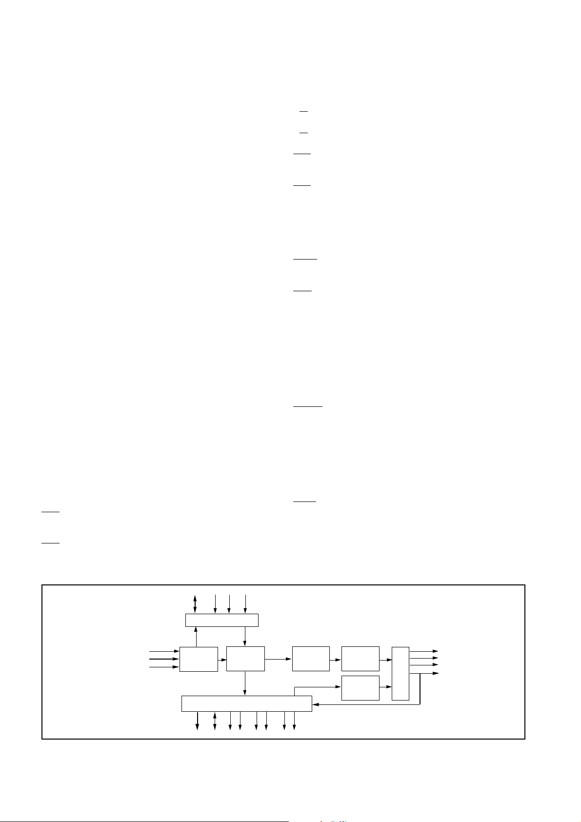
CBUS[7:0] CSTR CADR CEN
CONTROL I/F
DCLK
DIN[7:0]
DMODE[3:0]
INPUT
CONTROLLER
ADR[7:0] FS[15:0] OE1 OE2 RW1 RW2 RAS CAS
2
RUN LENGTH
DECODE &
INV ZIG ZAG
FRAME STORE CONTROLLER
Fig 2 : Simplified Block Diagram
TMS Test mode select for JTAG (Internally pulled high).
TRST JTAG reset pin (Internally pulled high).
TDI Input JTAG test data (Internally pulled high).
TDO Output JTAG test data.
NOTE:
"Barred" active low signals do not appear with a bar in the
main body of the text.
INVERSE
QUANTIZATION
INVERSE
DCT
LOW PASS
FILTER
ADD
FRMOUT
MBOUT
VPIX
YUV[7:0]

OPERATION OF MAJOR BLOCKS
-
-
-
-
-
-
-
VP2615
Run Length Decode
This block converts the run length coded data into 64
individual coefficient values, inserting zero value coefficients
where required. It then re-orders these 8 bit quantized DCT
coefficients from the zig zag arrangement into normal 8 x 8
format.
Inverse Quantise
This circuit reconstructs the 12 bit DCT coefficients from
the 8 bit quantized coefficients using the 5 bit Quantization
Value. This is performed using the following formulae.
If QUANT is odd :
REC = QUANT*(2*LEVEL+1) : LEVEL > 0
REC = QUANT*(2*LEVEL-1) : LEVEL < 0
If QUANT is even :
REC = QUANT*(2*LEVEL+1)-1 : LEVEL > 0
REC = QUANT*(2*LEVEL-1)+1 : LEVEL < 0
For Intra coded DC coefficients :
REC = 8*LEVEL
except if LEVEL=255 when REC=1024
If LEVEL=0 then REC=0 in all cases.
The reconstructed values (REC) are passed through a
clipping circuit in case of arithmetic overflow.
Inverse DCT
This circuit performs an Inverse Discrete Cosine Transform on an 8x8 block of 12 bit coefficients outputting 9 bit
signed pixel data. This IDCT fully meets the CCITT specification.
Frame Store Interface
The whole of the previous picture is stored in either two
external 64K x 16 DRAMs, or in a single 256 k x 16 DRAM, or
in four 256K x 4 DRAM's. A bit in the user defined Input Set Up
Data determines whether 64K or 256K DRAM's are to be
used. In the latter case, use OE1 as ADR8, RW1 as R/W and
do not connect RW2 and OE2.Table 1 specifies the worst case
maximum and minimum times which must be achieved by the
DRAM for correct operation with the VP2615. Times in the
DRAM specification must be less than or equal to the times
stated.
The Frame Store Interface manages all read and write
operations to these DRAM's. During the course of each
MacroBlock, the "Best Fit" MacroBlock is read from the
DRAMs and the fully processed MacroBlock is written back. In
this way, the previous frame is continually updated. The
DRAM controller also takes care of refresh for the DRAMs.
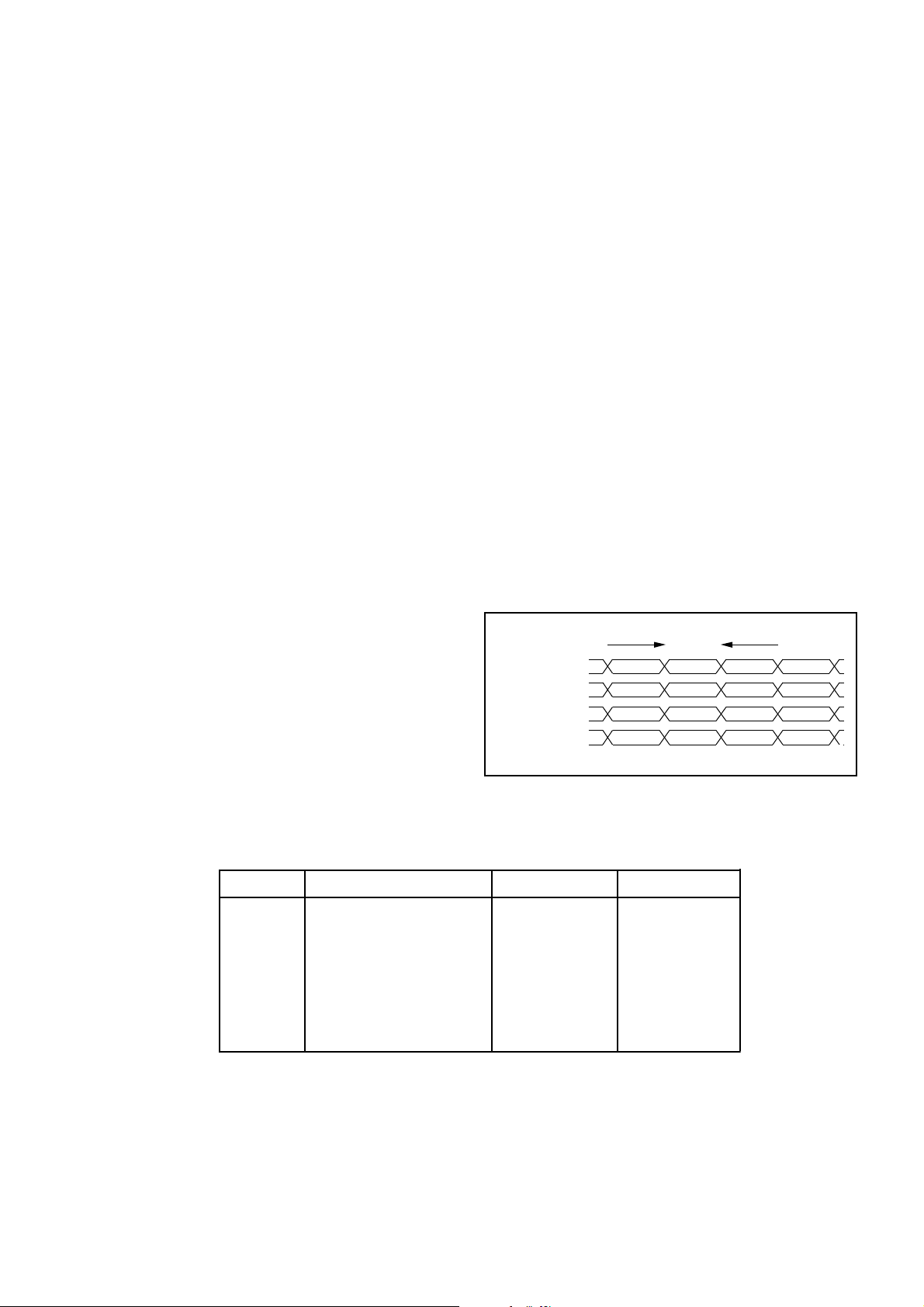
Figure 3 illustrates the effects of the pipeline delays
through the device; whilst macro block 3 is being input the
previous macroblock (2) is being decoded and needs the
equivalent macroblock from the previous frame to be read
from the frame store. At the same time macroblock 1, which
has already been decoded, is being written to the frame store
Minimum of
2048 cycles
DIN Input
Frame Store Read
Frame Store Write
YUV Output
MB3 MB4 MB5 MB6
MB2 MB3 MB4 MB5
MB1 MB2 MB3 MB4
MB1 MB2 MB3 MB4
Fig 3 : MacroBlock Pipelining
SYMBOL PARAMETER MINIMUM MAXIMUM
t RAC Access time from RAS
t CAC Access time from CAS
105ns or under
25ns or under
t RP RAS precharge time 50ns or under
t CP CAS precharge time 15ns or under
t RAS RAS pulse width 90ns or under
t CAS CAS pulse width 50ns or under
t REF Time to refresh 256 rows
0.25ms or over
N.B. All times are quoted assuming 27MHz operation. For lower clock
frequencies increase the above values proportionately.
Table 1. External DRAM Timing Requirements
3

VP2615
for use in the next frame and is also available on the output
pins.
Loop Filter
The best matched block from the search window in the
previous frame can be passed through a low pass filter to
reduce block boundary effects. The filter uses a simple [1 2 1]
characteristic in both horizontal and vertical dimensions as
laid down in the H261 Specification, on the macroblock
boundaries [010] is used. An instruction input at the DIN port
defines whether the filter should be used or not.
Reconstruction Adder
In Inter Mode, the IDCT data is added to the best fit block
from the previous frame store. In Intra Mode, the IDCT data is
added to zero. After the adder, the sign bit is removed from the
result to give 8 bit pixels. Clipping circuits ensure that any
pixels with values exceeding 255 are clipped to 255 and any
with negative values are clipped to zero (such values are
possible due to quantization effects).
OPERATION OF INTERFACES
DIN Input Port
The DIN port provides a glueless interface to the VP2614
Video Demultiplexer, from which it will accept run length
coded transform data and control information. The general
purpose nature of the interface will, however, allow other
sources of macroblock data to be used.
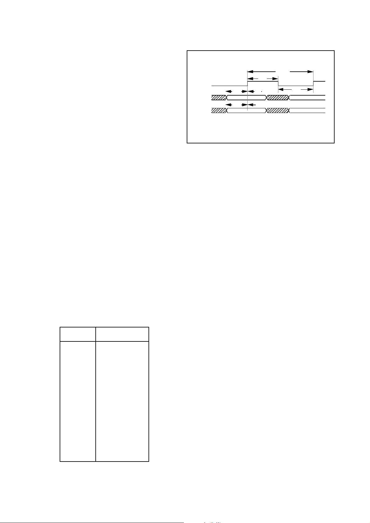
Data on the input bus is defined by means of the signals
DMODE3:0, and is strobed in with the DCLK signal which is
provided by the VP2614 and derived from SYSCLK. Set up
and hold times with respect to the rising edge of DCLK are
given in Figure 4. If DCLK is a continuous strobe, then the
WAIT state defined by DMODE 3:0 should be used to disable
any clocking actions. If preferred DCLK can alternatively be
DMODE3:0 FUNCTION
0000
0001
0010
0011
0100
0101
0110
0111
1000
1001
1010
1011
1100
1101
1110
1111
GOB Number
MB Number
Control Decisions
Quant Value
Horizontal MV
Vertical MV
Coded Blk Pattern
Sub-Block No
Zero Run Count
RLC Coefficient
Not used
Not used
Not used
Not used
Not used
Wait State
SCLK/2
20ns
DCLK
DIN7:0
DMODE3:0
10ns 2ns
10ns
N.B. All timings given are minimum values.
Fig 4 . DIN Port Timing
2ns
20ns
used as a strobe which is only present when data is valid and
action is needed. In this case WAIT states are not strictly
necessary.
The VP2615 always expects to receive a complete video
frame of data, even if error conditions have occurred in the demultiplexer. Skip Picture or Fixed Macroblocks should be
supplied if necessary once a frame has started. With the latter,
decoded data from the previously stored frame will be produced by the VP2615.
The asynchronous interface will allow the use of other
video de-multiplexers, as long as the protocol defined by
DMODE3:0 is observed. This protocol is defined below, and
summerized in Table 2.
Control Decisions : This byte must always be the first in the
sequence since it resets the internal control logic. It
defines which control decisions were taken when coding
the forthcoming MacroBlock. A high on DIN 0 indicates a
Fixed Macro Block (ie no change since the previous
frame), and a high on DIN1 indicates that Inter coding was
used. Similarly a high on DIN2 indicates that the
MacroBlock was filtered, a high on DIN3 indicates that
Motion Compensation was used. and a high on DIN6
indicates that SKIP PICTURE is in effect. In the latter case
the VP2615 will cease processing until SKIP PICTURE is
reversed by writing a new Control Decisions byte. Whilst
SKIP PICTURE is active, no further data will be output
from the YUV port. SKIP PICTURE effectively resets the
VP2615, and the next MacroBlock input should be the first
of a new frame. Since the frame store will not be updated
then the system should ensure that an Intra coded picture
is sent as soon as possible.
GOB Number: The correct GOB number is required for every
macro block in that group. (DIN3 is MSB).
MB Number: Each macroblock in a group requires an identi-
fication number. (DIN5 is MSB).
Coded Blk Pattern: This byte is defined in the H.261
Specification and is used to indicate which sub blocks
contain non zero coefficients. It is produced by the encoder
but is not used by the VP2615, and if provided will be
ignored. The sub block numbering sequence is actually
used to indicate blocks with zero coefficients.
Table 2 . DIN Mode Functions
Quant Value: This input represents the quantization value
4
 Loading...