MITEL VENUS-QP1T, VENUS-QP1S, VENUS-L, VENUS-KG Datasheet

Features
● Selectable dual RF input ports for 900MHz AMPS
and 1900MHz CDMA bands.
● Power Management Control
Description
VENUS-L is a dual integrated mixer circuit designed to
meet the IS95 and J-STD-008 receive system specifications operating in the 900 MHz and 1900MHz bands.
Venus-L is part of a complete chipset solution for CDMA
phones called the Planet chipset, and is built on a Mitel
advanced bipolar process with FT's of 25GHz.
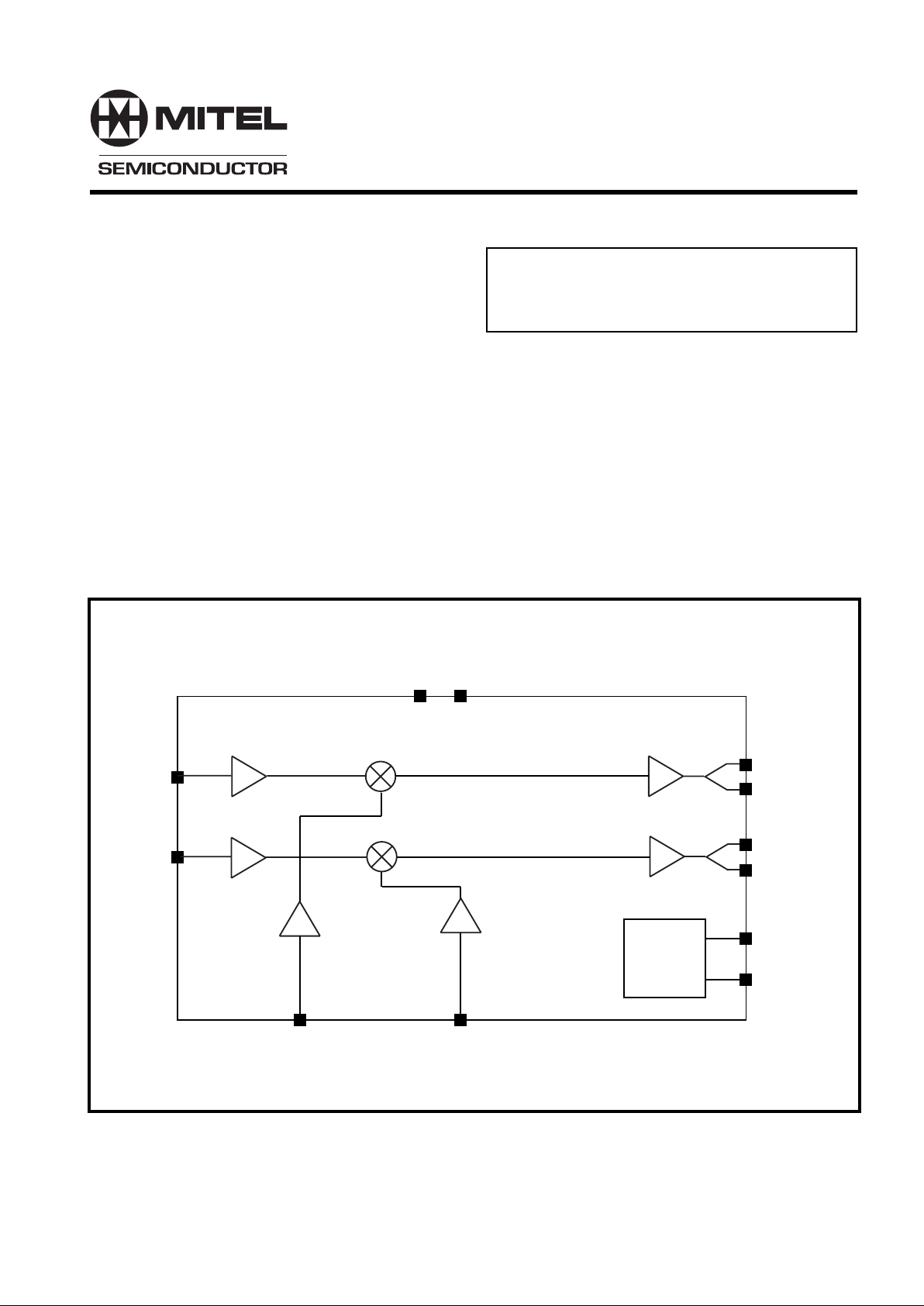
Figure 2. Block diagram
VENUS-L
CDMA/AMPS Dual Band RF Receiver
Preliminary Information
DS5082 Issue 2.1 J June 1999
GND
VCC
CDMA IF
CONTROL
CDMA IFB
AMPS IF
AMPS IFB
CHIP ENABLE
BAND 1900
LO 1GHZ
LO 2GHZ
RF 1900
RF 900
Ordering Iinformation
VENUS-L/KG/QP1S
VENUS-L/KG/QP1T

2
VENUS-L Preliminary Information
PIN 1
REF. SPOT
Figure1 Pin Connections
QSOP16
CDMA IF
CDMA IFB
VCC
LO 2GHZ
GND
RF 900
GND
CHIP ENABLE
BAND 1900
GND
RF 1900
GND
LO 1GHZ
VCC
AMPS IFB
AMPS IF
9
16
8
1
Circuit Description
The RF section of VENUS-L contains all of the circuitry
necessary to downconvert the RF signal from 900 MHz
or 1900 MHz to an IF of 50-250 MHz, and to correctly
interface with a suitable IF SAW filter. Two RF inputs are
provided, one for the 1900MHz band and one for the 900
MHz band. The required input is activated by means of
the ‘BAND 1900’ pin.
The input is a gm stage which will provide a
characteristic impedance to correctly terminate the RF
image-reject SAW filter.
Two LO ports are provided, one for 1900MHz band and
one for 900 MHz band, both with low noise buffer
amplifiers.
External matching components are required on the RF,
LO and IF ports.
Pin Description
Pin No Pin Name Description
1 CDMA IF CDMA (1900MHz mixer) IF SAW output
2 CDMA IFB CDMA (1900MHz mixer) IF SAW output bar
3 VCC Positive supply
4 LO 2GHZ 2 GHz LO input for 1900MHz mixer
5 GND Ground
6 RF 900 900MHz RF input
7 GND Ground
8 CHIP ENABLE Logic input for chip enable
9 AMPS IF AMPS (900MHz mixer) IF SAW output
10 AMPS IFB AMPS (900MHz mixer) IF SAW output bar
11 VCC Positive supply
12 LO 1GHZ 1GHz LO input for 900MHz mixer
13 GND Ground
14 RF 1900 1900MHz RF input
15 GND Ground
16 BAND 1900 Logic input to select 1900MHz or 900MHz signal path operation

3
Preliminary Information VENUS-L
Absolute Limits
Description Min. Typ. Max. Units Comments
Supply voltage, Vcc 4.0 V
Operating temperature, Top -30 70 deg C Pin temperature
Storage temperature, Tstg -40 125 deg C Ambient temperature
Junction temperature -30 125 deg C
Logic input high, VIH Vcc+0.6 V
Logic input low, VIL -0.6 V
Electrostatic Protection. High frequency RF device. This device has limited ESD protection on some pins (500V
Human body Model). Electrostatic handling precautions must be applied.
Description CHIP ENABLE BAND 1900 Comments
Standby Mode 0 X All circuits powered down
900MHz (AMPS) 1 0 900MHz (AMPS) signal path enabled
1900MHz (CDMA) 1 1 1900MHz (CDMA) signal path enabled
Electrical Characteristics (DC specification)
T
AMB
= -30°C to +70°C, VCC = +2.7 to +3.6V. These characteristics are guaranteed by either production test or
design. They apply within the specified ambient temperature and supply voltage ranges unless otherwise stated.
Operating Modes
Characteristic Value Units Conditions
Min Typ Max
General
Supply voltage 2.7 3.0 3.6 V All Vcc pins.
Operating. Temperature -30 25 70 deg C Ambient
Current Consumption
Standby Mode, RF section 10 100 µA
1900MHz Mode operation 15 mA
900MHz Mode operation 13 mA
Control Logic
Input logic high, VIH Vcc-0.5 Vcc+0.1 V All logic inputs
Input logic low, VIL -0.1 0.5 V All logic inputs
Input high current, IIH -10 10 µA All logic inputs
Input low current, IIL -10 10 µA All logic inputs
 Loading...