MITEL SP8861 Datasheet

SP8861
1·3GHz Low Power Single-Chip Frequency Synthesiser
Supersedes version in the1996 Professional Products IC Handbook, HB2480 - 3.0 DS3640 - 4.0 April 1998
The SP8861 is a low power single chip synthesiser
intended for professional radio applications, containing all the
elements (apart from the loop amplifier) required to build a PLL
frequency synthesis loop
The device is serially programmable by a three-wire data
highway and contains three independent buffers to store one
reference divider word and two local oscillator divider words.
A digital phase detector with two charge pumps,
programmable in phase and gain, are provided to improve
lock-up performance. The preset operation of the charge
pumps can be overwritten or the comparison frequencies
switched to output ports under control of the divider word. The
dual modulus ratio and so operating range is also
programmable through the same word.
A power down mode is incorporated as a battery economy
feature.
FEATURES
■ Improved Digital Phase Detector Eliminates
‘Dead Band’ Effects
■ Low Operating Power, Typically 175mW
■ 1·3GHz Operating Frequency
■ Complete Phase Locked Loop
■ High Input Sensitivity
■ Programmed throughThree-Wire Bus
■ Wide Range of Reference Division Ratios
■ Local Storage for Two Frequency Words, giving
Rapid Frequency Toggling
■ Programmable Phase Detector Gain
■ Power Down Mode
4321282726
5
F
*
REF
POWER DOWN
RF INPUT
RF INPUT
*FPD and F
6
7
4
V
EE
8
V
4
CC
9
V
1
CC
10
11
12 13 14 15 16 17 18
outputs are reversed by the phase
REF
detector sense bit in the F1/F2 programming word. The
above diagram is correct when the sense bit is low. See
Table 2 and Fig. 7.
V
1, VEE1 – preamplifier and prescaler supplies
CC
VCC2, VEE2 – oscillator supplies
V
3, VEE3 – charge pump 2 supplies
CC
VCC4, VEE4 – ECL supplies
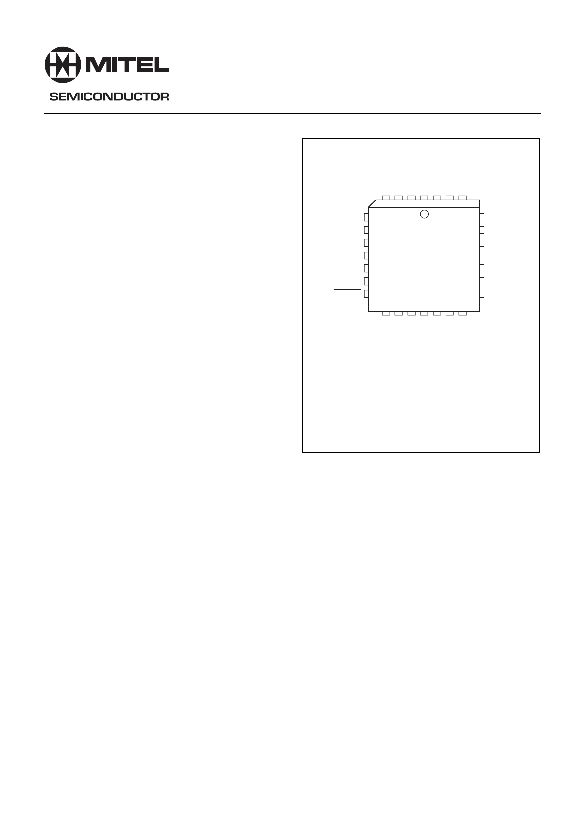
Fig. 1 Pin identification diagram (top view)
*
PD
PD1 OUTPUT
F
SP8861
1
EE
V
F1/F2
3
EE
V
ICCdLOCK DETECT
DATA
CLOCK
NC
ENABLE
NC
2
CC
V
25
24
23
22
21
20
19
PD2 OUTPUT
RPD
3
V
CC
GROUND
XTAL 1
XTAL2
V
2
EE
HP28
ABSOLUTE MAXIMUM RATINGS
Supply voltage
Storage temperature
Operating temperature
Prescaler input voltage
20·3V to 17V
255°C to 1150°C
240°C to 185°C
2·5V p-p
ORDERING INFORMATION
SP8861/NA/HP

SP8861
RF INPUT
RF INPUT
F1/F2
DATA
CLOCK
ENABLE
POWER
DOWN
10
11
13
14
15
16
6
DATA
INPUT
16/17 OR 8/9
CONTROL
LOGIC
2-BIT
SR
A COUNT
1LOGIC
4 BIT
N0 N3 N4 N18 N19 N20 N21
N0 N12 N14 N15N13
R
COUNT
REFERENCE
DIVIDER
M COUNT
1LOGIC
15 BIT
22 BIT SHIFT REGISTER
1 BIT13 BIT 2 BIT
*
F
REF
f
PD
DUAL
F1/F2
2 BIT 1 BIT
DATA
BUFFER
SINGLE
REFERENCE
BUFFER
LOGIC
f
REF
and FPD outputs are reversed by the phase detector
PHASE
DETECTOR
CHARGE
PUMP 1
CHARGE
PUMP 2
OUTPUT
INTERFACE
3
24
28
25
27
5
4
PD1
RPD
Cd
PD2
LOCK
DETECT
*
F
REF
FPD*
sense bit in the F1/F2 programming word. The pin allocations
shown are correct when the sense bit is low (see Table 2 and Fig. 7).
21
20
CRYSTAL
f
REF
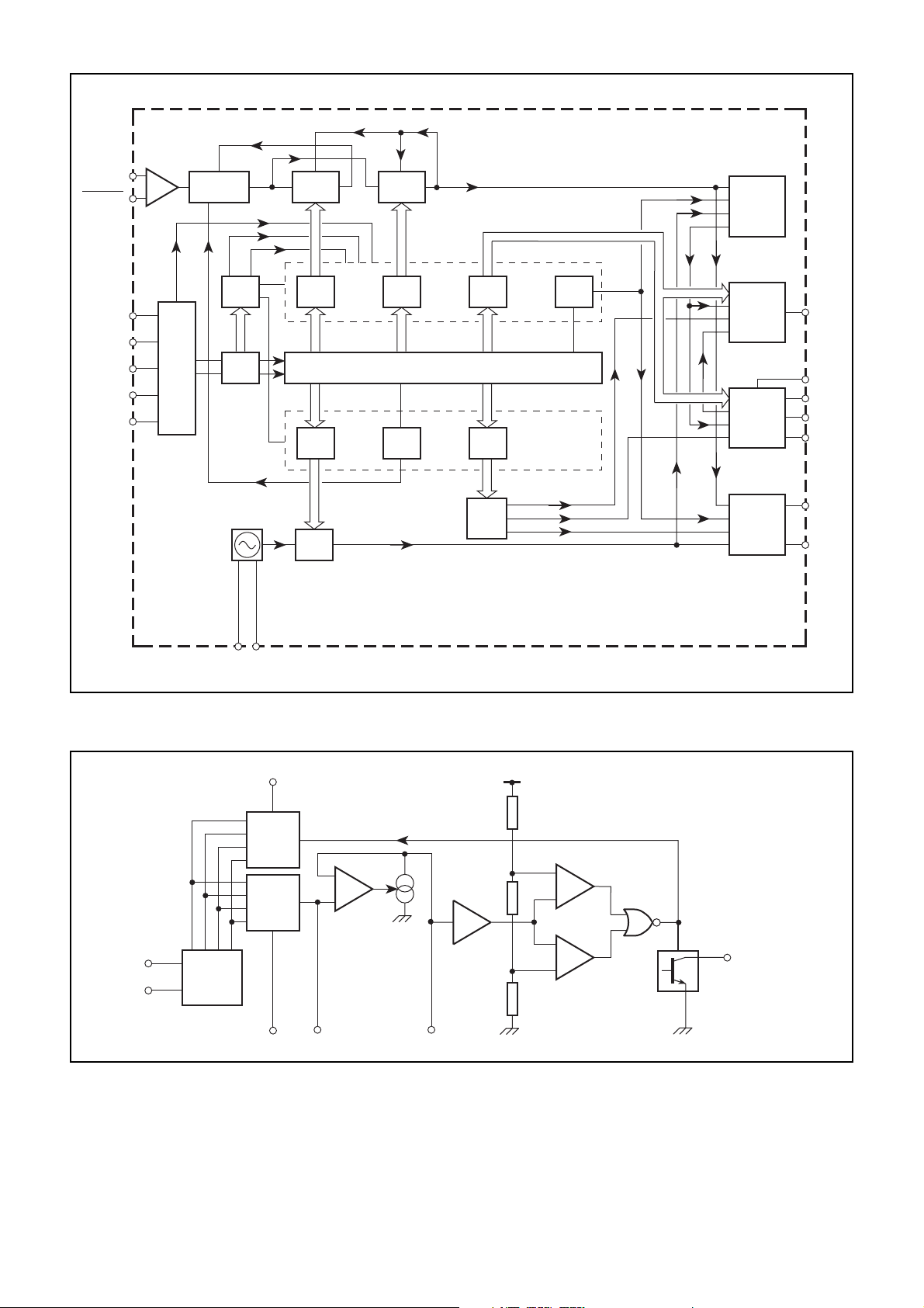
Fig. 2 SP8861 block diagram
V
PD1
3
CHARGE PUMP 1 DISABLE
CHARGE
PUMP 1
(SEE TABLE 4)
−
CHARGE
PUMP 2
f
PD
PHASE
DETECTOR
24
RPD
31
+
TRANSCONDUCTANCE
AMPLIFIER
25
PD2
31
31 BUFFER
28
Cd
CC
Output current at pin 27 is proportional to
voltage difference between pins 25 and 28,
45k
I
= 625µA
MAX
−
10k
45k
+
−
+
DUAL VOLTAGE
COMPARATOR
27
LOCK DETECT
Fig. 3 Detailed block diagram of lock detect circuit
2

400
SP8861
350
300
250
200
150
100
INPUT VOLTAGE (mV RMS)
50
25
0
0
GUARANTEED
OPERATING
4
TYPICAL OVERLOAD
WINDOW
8/9 MODE
500
GUARANTEED
OPERATING
WINDOW
4
16/17 MODE
650 750
1000 1300 150015080
FREQUENCY (MHz)
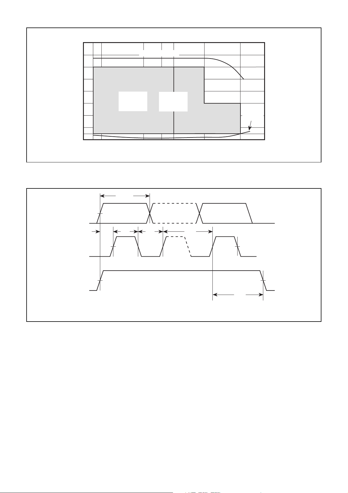
Fig. 4 Typical input characteristics and input drive requirements for SP8861
tS1t
CH
DATA
2V
LAST DATA BITFIRST DATA BIT
TYPICAL
SENSITIVITY
CLOCK
ENABLE
t
REP
t
S
2V
= 1µs min., t
t
CH
= 50ns min., tCH = 50ns min., tCL = 100ns min., tE = 50ns min.
S
t
CL
t
REP
2V
t
E
Fig. 5 Data and clock timing requirements
3

SP8861
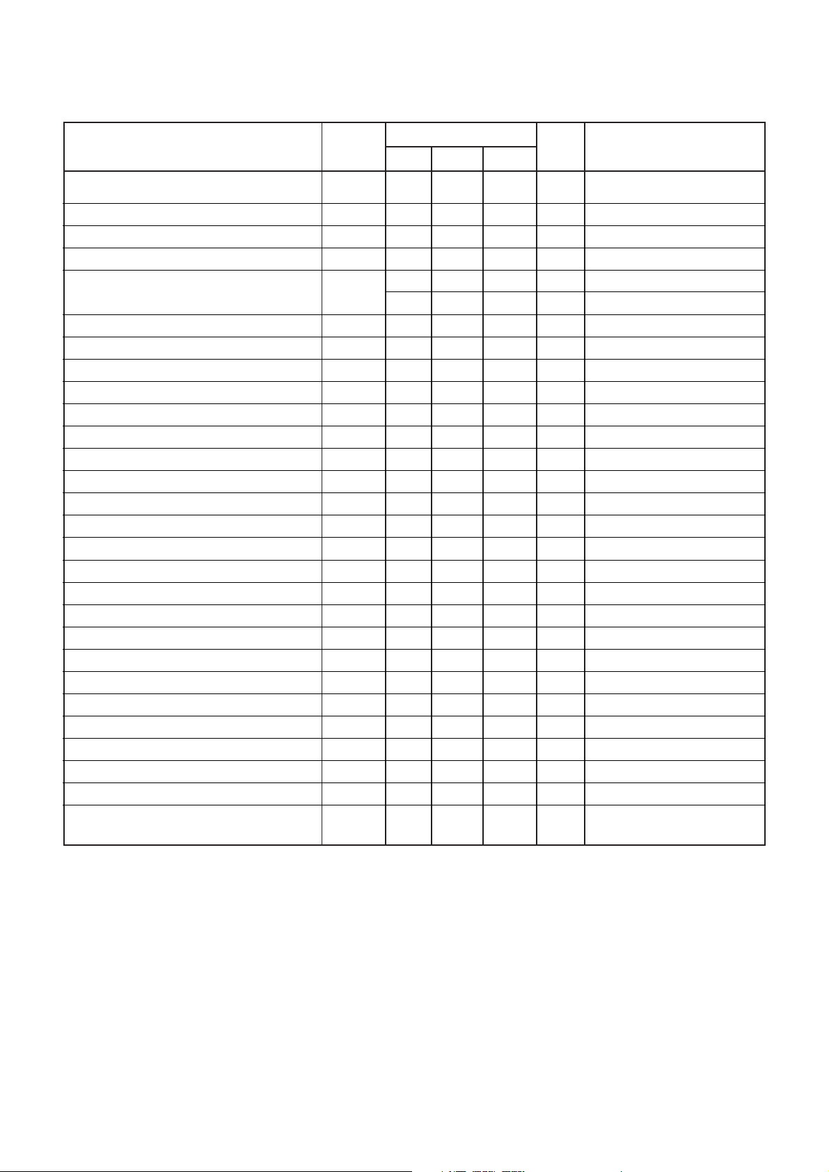
ELECTRICAL CHARACTERISTICS
These characteristics are guaranteed over the following range of operating conditions unless otherwise stated:
Supply voltage VCC = 14·75V to 15·25V. T
= 255°C to 1125°C (A Grade), 240°C to 185°C (B Grade)
AMB
Characteristic Conditions
Supply current
Supply current in power down mode
Input sensitivity
Input overload
RF input division ratio
Comparison frequency
Reference oscillator input frequency
External reference input voltage
Reference division ratio
Data clock repetition rate, t
Minimum setup time, t
REP
S
DATA input high
DATA input low
CLOCK input high
CLOCK input low
Data ENABLE high
Data ENABLE low
F1/F2 input high
F1/F2 input low
POWER DOWN input high
POWER DOWN input low
F1/F2 input current
POWER DOWN input current
RDP external resistance
LOCK DETECT output voltage when in lock
LOCKDETECT switching voltage high
LOCK DETECT switching voltage low
F
and F
PD
output voltage swing
REF
Pin
8,9,18,23
8
10,11
10,11
10,11,4
4,5
20,21
20
20,5
15
14,15
14
14
15
15
16
16
13
13
6
6
13
6
24
27
25
25
Min.
256
56
10
50
0·6V
V
0·6V
V
0·6V
V
0·6V
V
0·6V
V
68
2·7
4
1
CC
EE
CC
EE
CC
EE
CC
EE
CC
EE
Value
Typ. Max.
33
4·5
40
6
524287
262143
5
20
500
8191
1
V
CC
0·3V
V
CC
0·3V
V
CC
0·3V
V
CC
0·3V
0·9V
0·3V
5
5
330
1
2·3
0·9
CC
CC
CC
CC
CC
CC
Units
mA
mA
MHz
MHz
mVrms
µs
ns
V
V
V
V
V
V
V
V
V
V
µA
µA
kΩ
V
V
V
V
See Fig. 4
See Fig. 4
With 416/17 selected
With 48/9 selected
See Fig. 5
See Fig. 5
F1 buffer selected
F2 buffer selected
V pin 13 = 5·0V
V pin 6 = 4·5V
I pin 27 = 1mA
= 5V
V
CC
= 5V
V
CC
= 5V, external pulldown
V
CC
may be required
4
 Loading...