MITEL GP2021IG, GP2021GQ1R, GP2021 Datasheet
The GP2021 is a 12 channel C/A code baseband
correlator for use in NAVSTAR GPS and GLONASS satellite
navigation receivers. The GP2021 complements the GP2015
and GP2010 C/A code RF downconverters available from
Mitel Semiconductor.
The GP2021 is compatible with most 16 bit and 32 bit
microprocessors, especially those from Motorola and Intel,
with additional on–chip support for the ARM60 32 bit RISC
processor. When the ARM60 is used, the on–chip memory
management functions allow implementation of a full GPS
receiver with minimal external logic.
The GP2021 allows individual channel de–activation, for
systems not requiring full 12 channel operation, to save power
and processor loading. Receiver power may be further
conserved by reducing the supply voltage to 2.2V under
battery backup. Although all system functions are disabled,
the 32.768kHz oscillator and Real Time Clock are maintained
for the microprocessor to estimate satellite visibility at power
on to reduce signal acquisition time.
A development system called the GPS Architect is
available as a basis for receiver design using the GP2021 and
associated products.
FEATURES
■ 12 Fully Independent Correlation Channels
■ 1PPS UTC Aligned Timing Output
■ On–Chip Dual UART and Real Time Clock
■ Compatible with most 16 and 32 bit Microprocessors
■ Memory Control Logic for ARM60 Microprocessor
■ Low Voltage, Low Current Power–Down Mode
■ Power Dissipation 150mW Typical
■ Compatible with GP2015 and GP2010 RF Front Ends
■ Battery Backup Voltage 2.2V (min)
APPLICATIONS
■ GPS Navigation Systems
■ High Integrity Combined GPS–GLONASS Receivers
■ GPS Geodetic Receivers
■ Time Transfer Receivers
ORDERING INFORMATION
GP2021/IG/GQ1R
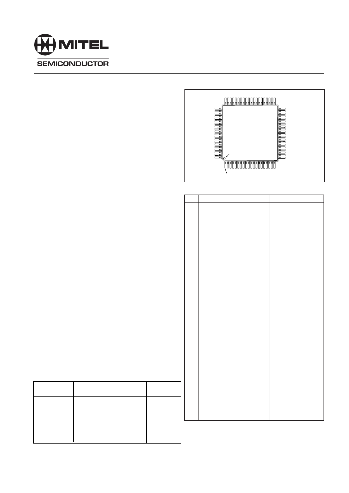
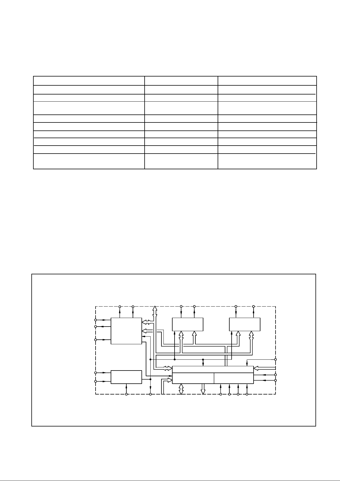
Fig.1 Pin connections - top view
GQ80
GP2021
PIN 1
PIN 1 IDENT
PIN
1
2
3
4
5
6
7
8
9
10
11
12
13
14
15
16
17
18
19
20
21
22
23
24
25
26
27
28
29
30
31
32
33
34
35
36
37
38
39
40
DESCRIPTION
MULTI_FN_IO
POWER _GOOD
NRESET_OP
NARMSYS
XIN
XOUT
TXA
TXB
RXA
RXB
NROM / NC
NEEPROM / NC
NSPARE_CS / NC
V
DD
V
SS
NRAM / BC
NW0 / NC
NW1 / NC
NW2 / NC
NW3 / NC
NRD / NC
ARM_ALE / NC
DBE / NC
ACCUM_INT
MEAS_INT
NBW / WRPROG
NMREQ / DISCIP2
NOPC / NINTELMOT
NRW / DISCIP3
MCLK / NC
ABORT / MICRO_CLK
DISCIO
A22 / READ
VDD
VSS
A21 / NCS
A20 / WREN
A9
A8
A7
DESCRIPTION
A6
A5
A4
A3
A2
A1 / ALE_IP
A0 / NRESET_IP
D0
D1
D2
D3
D4
D5
D6
V
DD
V
SS
D7
D8
D9
D10
D11
D12
D13
D14
D15
PLL_LOCK
VDD
DISCOP
V
SS
CLK_T
CLK_I
V
SS
SAMPCLK
V
DD
NBRAM / DISCIP4
SIGN0
MAG1
SIGN1
MAG1
DISCIP1
PIN
41
42
43
44
45
46
47
48
49
50
51
52
53
54
55
56
57
58
59
60
61
62
63
64
65
66
67
68
69
70
71
72
73
74
75
76
77
78
79
80
DS4077 - 2.6 July 1996
GP2021
GPS 12 channel Correlator
Advance Information
RELATED PRODUCTS
PART DESCRIPTION DATASHEET
REFERENCE
GP2015 GPS Receiver RF Front End DS4374
– TQFP 48 package
GP2010 GlPS Receiver RF Front End DS4056
– PQFP 44 package
DW9255 35.42MHz SAW Filter DS3861
P60ARM 32 bit RISC Microprocessor DS3553
GPS Architect GPS 12 Channel DS4004
Receiver Development System

2
GP2021
TABLE OF CONTENTS
HEADING PAGE
TYPICAL GPS RECEIVER 4
PIN DESCRIPTION 4
Differences between Real and Complex_Input Mode 7
FUNCTIONAL DESCRIPTION 7
12 CHANNEL CORRELATOR 8
Clock Generator 8
Timebase Generator 8
Status Registers 9
Sample Latches 9
Address Decoder 9
Bus Interface 9
TRACKING MODULES 9
Carrier DCO 9
Code DCO 9
Carrier Cycle Counter 9
C/A Code Generator 9
Source Selector 10
Carrier Mixers 10
Code Mixers 10
Accumulate and Dump 10
Code Phase Counter 10
Code Slew Counter 10
Epoch Counter 11
PERIPHERAL FUNCTIONS 11
Dual UART 11
Receiver 11
Transmitter 11
Reset 11
Channel Loopback 12
Real Time Clock (RTC) and Watchdog 12
Power and Reset Control 12
Power Down Mode 12
Hardware Reset Generation 13
System Error Status Register 13
Discrete I/O 14
Digital System Test Interface 15
MICROPROCESSOR INTERFACE 15
General Interface Timing 15
Write Cycle to Read Cycle Timings 15
Write Cycle to Write Cycle Timings 15
Notes about Interface Timing Constraints 15
ARM System Mode 17
Address Map 17
Control Signals 17
ARM System Timing 17
Wait State Generation 17
Debug (Abort) Function 20
Standard Interface Mode 20
Control Signals 21
Motorola Style Interface 21
Intel 80186 Style Interface 21
Intel 486 Style Interface 21
Reset 21
Register Addressing 21
CONTROLLING THE GP2021 22
Search Operation 22
Carrier DCO Programming 22
Code DCO Programming 22
Code Generator Programming 22
Reading the Accumulated Data 22
Search on Other Code Phases 22
Data Bit Synchronisation 22
Reading the Measurement Data 22
Preset Mode 23

3
GP2021
Interrupts 23
Signal Path Delay (Introduced by Hardware Signal Processing) 23
Integrated Carrier Phase Measurement 23
Timemark Generation 24
GP2021 Register Map 25
Correlator Registers 26
Tracking Channel Registers 27
ACCUM_STATUS_A 28
ACCUM_STATUS_B 28
ACCUM_STATUS_C 28
CHx_ACCUM_RESET 29
CHx_CARRIER_CYCLE_COUNTER 29
CHx_CARRIER_CYCLE_HIGH 29
CHx_CARRIER_DCO_INCR_HIGH 29
CHx_CARRIER_DCO_PHASE 29
CHx_CODE_DCO_INCR_HIGH 30
CHx_CODE_DCO_PHASE 30
CHx_CODE_DCO_PRESET_PHASE 30
CHx_CODE_PHASE 30
CHx_CODE_SLEW 30
CHx_EPOCH_CHECK 31
CHx_EPOCH 31
CHx_EPOCH_COUNT_LOAD 31
CHx_I_TRACK, CHx_Q_TRACK, CHx_I_PROMPT,CHx_Q_PROMPT 31
CHx_SATCNTL 31
MEAS_STATUS_A 33
MULTI_CHANNEL_SELECT 33
PROG_ACCUM_INT 33
PROG_TIC_HIGH, PROG_TIC_LOW 34
RESET_CONTROL 34
STATUS 35
SYSTEM_SETUP 35
TEST_CONTROL 35
TIMEMARK_CONTROL 36
X_DCO_INCR_HIGH 37
Peripheral Functions Registers 37
Real Time Clock and Watchdog 37
RTC_LS, RTC_2ND, RTC_MS 37
CLOCK_RESET 37
WATCHDOG_RESET 37
DUART 38
CONFIG_A, CONFIG_B 38
STATUS_A, STATUS_B 38
RESET_A, RESET_B 38
TX_DATA_A, TX_DATA_B, RX_DATA_A, RX_DATA_B 38
TX_RATE_A, TX_RATE_B 39
System Control 39
WAIT_STATE 39
SYSTEM_CONFIG 39
SYSTEM_ERROR_STATUS 39
CHIP_REVISION 39
DATA_RETENT 40
General Control 40
IO_CONFIG 40
TEST_CONFIG 41
DATA_BUS_TEST 41
ABSOLUTE MAXIMUM RATINGS 41
Electrostatic Discharge Protection (ESD) 41
Crystal Specification 41
ELECTRICAL CHARACTERISTICS 42
PIN TYPES 44
TIMING CHARACTERISTICS 47
PACKAGE DETAILS 64
DETAILED DESCRIPTION OF REGISTERS 25
4
GP2021
TYPICAL GPS RECEIVER
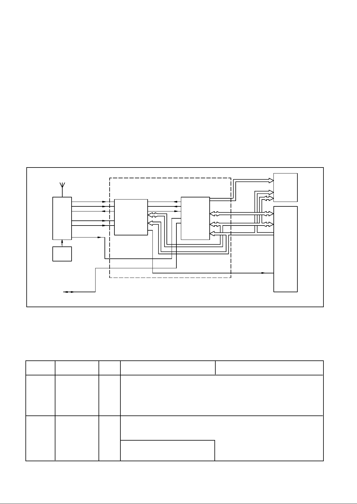
Fig. 2 shows a typical GPS receiver employing a GP2010
RF front–end, a GP2021 correlator and an ARM60 32 bit RISC
microprocessor.
A single front end may be used, since all GPS satellites use
the same L1 frequency of 1575.42 MHz. However, in order to
achieve better sky coverage, it is sometimes desirable to use
more than one antenna. In this case, separate front ends will
be needed.
The RF section, GP2010, performs down conversion of
the L1 signal for digital baseband processing. The resultant
signal is then correlated in the GP2021 with an internally
generated replica of the satellite code to be received.
Individual codes for each channel may be selected
independently to enable acquisition and tracking of up to 12
different satellites simultaneously
The results of the correlations form the accumulated data
and are transferred to the microprocessor to give the
broadcast satellite data (the ’Navigation Message’) and to
control the software signal tracking loops.
The GP2021 can be interfaced to one of two styles of front
end. In Real_Input mode, the front end supplies either a 1
(sign) or 2 (sign and magnitude) bit signal to either the
SIGN0/MAG0 or SIGN1/MAG1 inputs of the GP2021.
Alteratively, in Real_Input mode, 2 separate front ends can be
connected to a single GP2021 and selected under software
control. The GP2015 and GP2010 are Real_Input mode front
ends.
In Complex_Input mode, the front end is required to supply
In–phase (I) and Quadrature (Q) signals to the SIGN0/MAG0
and SIGN1/MAG1 inputs respectively. Hence, only a single
front end can be used with each GP2021 in Complex_Input
mode.
GP2010
SIGN
MAG
SAMPCLK
CLK_T
CLK_I
PLL_LOCK
10MHz
TCXO
TX/RX
SERIAL
COMMS PORT
ACCUM_INT,MEAS_INT
12
CHANNEL
CORRELATOR
WREN
READ
MICRO_CLK PERIPHERAL
FUNCTIONS
MEMORY
CONTROL
MEMORY
CONTROL
DATA
ADDR
ARM60
GP2021
L1
ANTENNA
Fig. 2 Block diagram of typical ARM based receiver
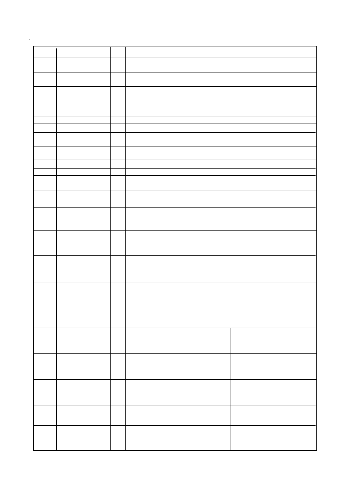
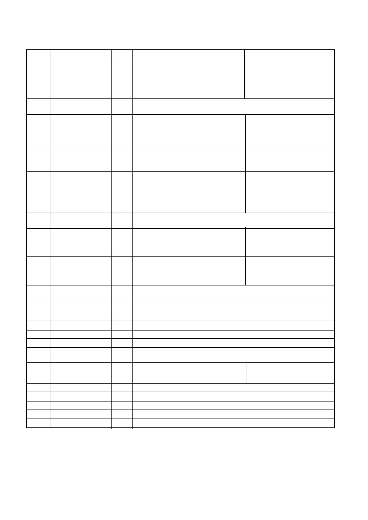
PIN DESCRIPTION
All V SS and V DD pins must be connected in order to ensure reliable operation. Any unused inputs must be tied High or Low.
The Table below describes the pin functions in Real_Input mode and assumes a master clock input frequency of 40MHz.
Those pins whose functions differ in Complex_Input mode are described at the end of the table.
Note that those pin names containing a ‘/’ have dual functionality between ARM System and Standard Interface modes. The
Pin mnemonic for ARM System mode always precedes the ‘/’.
Pin No Signal Name Type Description ARM System Mode Description Standard Interface
Mode
15, 35, V SS - Ground Pin
56, 69,
72
14, 34, V DD + Power supply to device.
55, 67,
74
1 MULTI_FN_IO I/O Multi–function input / output. Its function is configured by the IO_CONFIG register.
After a GP2021 reset it acts as the Digital System Test Enable input. It can also
be configured as a discrete output, or a discrete input if certain conditions are met.
Can be configured as the TRIGGER
input to the DEBUG block in ARM
System mode.
5
GP2021
Pin No Signal Name Type Description ARM System Mode Description Standard Interface
Mode
2 POWER_GOOD I Power Monitor input. High for normal operation. Low forces the GP2021 into
Power Down mode.
3 NRESET_OP O System Reset output (Active Low). Lasts for 4 MICRO_CLK cycles after all reset
conditions have cleared.
4 NARMSYS I Processor Mode Selection input. When Low, this input selects ARM System
mode. When High, Standard Interface mode is selected.
5 XIN I Crystal input connection to Real Time Clock.
6 XOUT O Crystal output connection from Real Time Clock.
7 TXA O Transmit Data output from Channel A of the Dual UART.
8 TXB O Transmit Data output from Channel B of the Dual UART.
9 RXA 1 Receive Data input to Channel A of the Dual UART. This pin acts as a master clock
input in Digital System Test mode.
10 RXB I Receive Data input to Channel B of the Dual UART. This pin acts as the Real Time
Clock reset in Digital System Test mode.
11 NROM / NC O ROM Chip Select output (Active Low). Unused output. (Do not connect.)
12 NEEPROM / NC O EEPROM Chip Select output (Active Low) Unused output. (Do not connect.)
13 NSPARE_CS / NC O Spare Chip Select output (Active Low). Unused output. (Do not connect.)
16 NRAM / NC O RAM Chip Select output (Active Low). Unused output. (Do not connect.)
17 NW0 / NC O Byte 0 Write Strobe output (Active Low). Unused output. (Do not connect.)
18 NW1 / NC O Byte 1 Write Strobe output (Active Low). Unused output. (Do not connect.)
19 NW2 / NC O Byte 2 Write Strobe output (Active Low). Unused output. (Do not connect.)
20 NW3 / NC O Byte 3 Write Strobe output (Active Low). Unused output. (Do not connect.)
21 NRD / NC O Read Data Strobe output (Active Low). Unused output. (Do not connect.)
22 ARM_ALE / NC O ALE output to the microprocessor Unused output. (Do not connect.)
(Active High). Controls the transparent
latches at the microprocessor address
outputs.
23 DBE / NC O Data Bus Enable output to the Unused output. (Do not connect.)
microprocessor. When Low, places the
microprocessor data bus drivers in a
high impedance state.
24 ACCUM_INT O A free running interrupt to the microprocessor. It allows control of data transfer
between the accumulators in the correlator and the microprocessor. It is active
Low when configured for ARM System mode or Motorola mode and is active High
in Intel mode.
25 MEAS_INT O An interrupt to the microprocessor. It allows control of measurement data transfer
between the correlator and the microprocessor. It is active Low when configured
for ARM System mode or Motorola mode and is active High in Intel mode.
26 NBW / WRPROG I Byte/Word input from the Write–Read Program input. In Intel
microprocessor. Low indicates a byte mode, High selects 486 style
transfer, and High a word transfer. interface and Low 186 style.
Unused in Motorola mode
27 NMREQ / DISCIP2 I Memory Request input from the Multi–purpose discrete input.
microprocessor. Low indicates that the
microprocessor requires a memory
access during the following cycle.
28 NOPC / NINTELMOT I Opcode fetch input from the High selects Motorola mode and
microprocessor. Low indicates that an Low Intel mode.
instruction is being fetched and High
that data is being transferred.
29 NRW / DISCIP3 I Read/Write Select input from the Multi–purpose discrete input.
microprocessor. Low indicates a read
cycle and High a write cycle.
30 MCLK / NC O Microprocessor Clock output Unused output. (Do not connect.)
(nominally 20MHz). Its phases can be
stretched under control of the
Microprocessor Interface.
6
GP2021
Pin No Signal Name Type Description ARM System Mode Description Standard Interface
Mode
31 ABORT/ MICRO_CLK O Abort output to the microprocessor. 20MHz Clock output. Provides a
Generates a valid ARM Data Abort 20MHz clock with a 1:1
sequence, triggered by a rising edge mark-to-space ratio
at MULTI_FN_IO if this function is
enabled.
32 DISCIO I/O Multi–purpose discrete input / output. After a GP2021 reset it is
configured as an input.
33 A22 / READ I Address input from the microprocessor. Read input from the
A<22:20> are decoded to select the microprocessor. In Intel mode
address space partitioning. it is the active Low read strobe.
In Motorola mode it is the Read
(High)/Write (Low) select line.
36 A21 / NCS I Address input from the microprocessor. GP2021 Chip Select input
A<22:20> are decoded to select the (Active Low).
address space partitioning.
37 A20 / WREN I Address input from the microprocessor Write–Read Strobe input from
A<22:20> are decoded to select the the microprocessor. In Intel
address space partitioning. mode it is the active Low write
strobe. In Motorola mode it is
the active High Write-Read
strobe.
38 – 45 A<9:2> I Address Inputs <9:2> from the microprocessor. These allow register
selection.
46 A1 / ALE_IP I Address input 1 from the Address Latch Enable input
microprocessor. A<1:0> are decoded from microprocessor (Active
to provide individual byte write High)
selection via NW<3:0>.
47 A0 / NRESET_IP I Address input 0 from the Reset input (Active Low).
microprocessor. A<1:0> are decoded
to provide individual byte write
selection via NW<3:0>.
48– 54, D<0:15> I/O Bidirectional data bus.
57–65
66 PLL_LOCK I PLL Lock Indicator input from RF section. When High this signa
indicates that the PLL within the RF section is in lock and the master
clock inputs have stabilised.
68 DISCOP O Multi–purpose discrete output.
70 CLK_T I Master clock input (40MHz).
71 CLK_I I Inverted Master clock input.
73 SAMPCLK O Sample Clock output to the front end. Provides a 5.714MHz clock with a
4:3 mark–to–space ratio.
75 NBRAM / DISCIP4 I Battery Backed RAM select input. Multi–purpose discrete input.
Defines the state of the NRAM output in
Power Down mode.
76 SIGN0 I SIGN0 input from the RF section.
77 MAG0 I MAG0 input from the RF section.
78 SIGN1 I SIGN1 input from a second, optional, RF section.
79 MAG1 I MAG1 input from a second, optional, RF section.
80 DISCIP1 I Multi–purpose discrete input.
7
GP2021
Difference between Real and Complex_Input
Mode
The input mode is selected by theFRONT_END_MODE bit
in the SYSTEM_SETUP register. It defaults to Real_Input
mode at power up. The differences between Real and
Complex input mode are summarised in the following table.
Description Real_Input mode Complex_Input mode
Recommended Master clock frequency 40MHz 35MHz
GP2021 internal clocking
1
± 7 ÷ 6
MICRO_CLK 2 output frequency 20MHz 17.5MHz
mark : space 1:1 1:1
Pin No 76 SIGN 0 SIGN_I
Pin No 77 MAG 0 MAG_I
Pin No 78 SIGN 1 SIGN_Q
Pin No 79 MAG 1 MAG_Q
Input Signal Sampling Rate 5.714MHz 5.833MHz
SAMPCLK output frequency 5.714MHz Not available
mark : space 4:3 (held Low)
)
Notes. 1 The GP2021 interrupt and TIC timebase dividers are clocked by this resulting clock.
2 The MCLK output is derived from this signal. In ARM mode the phases of MCLK are stretched by the
Microprocessor Interface block.
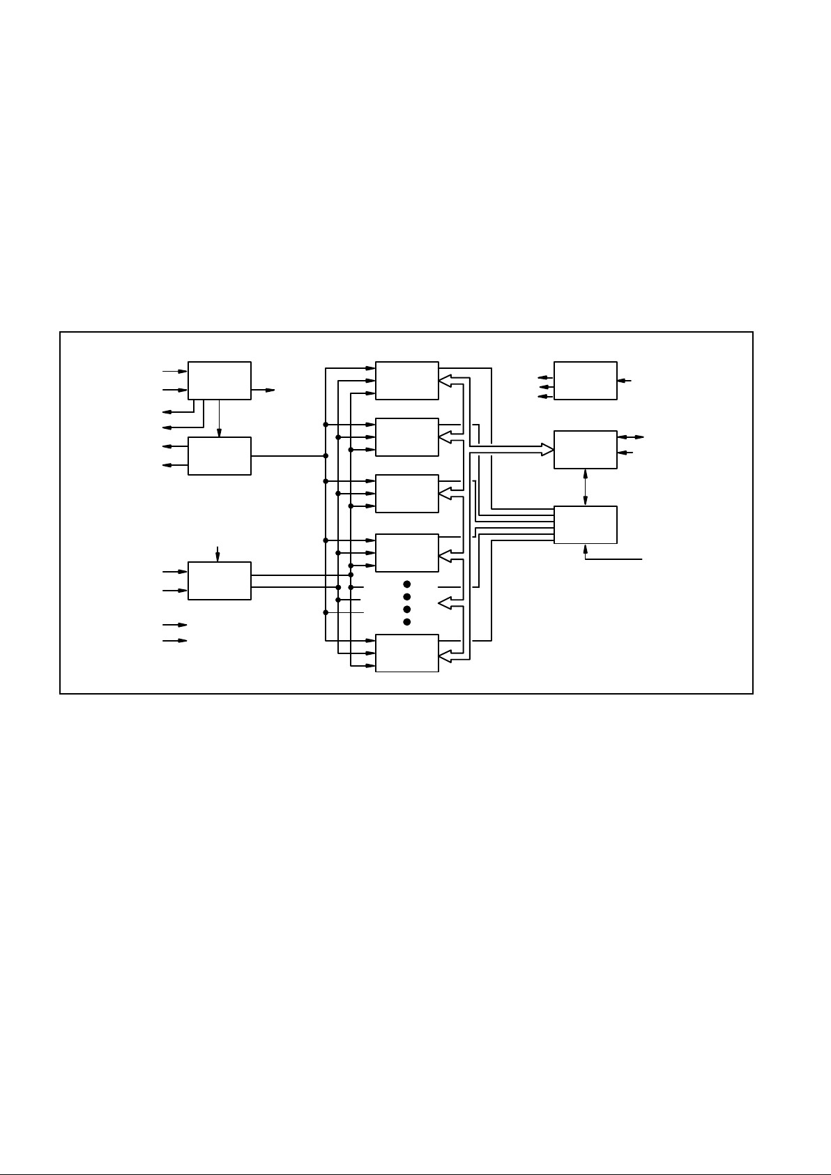
FUNCTIONAL DESCRIPTION
The GP2021 incorporates a 12 Channel GPS Correlator,
together with microprocessor support functions including a
Dual UART, a Real Time Clock and Memory Control Logic for
the ARM60 microprocessor. It can be configured for either
ARM System mode or Standard Interface mode. A block
diagram of the GP2021 is shown in Fig. 3.
Whilst in ARM System mode the Memory Control Logic
allows an ARM60 microprocessor to interface with the
Correlator, Real Time Clock, Dual UART and a variety of
memory devices (i.e.
SRAM, EPROM, Flash and EEPROM), without the need for
external glue logic.
In Standard Interface mode the GP2021 allows most 16
and 32 bit microprocessors to interface with the Correlator,
Real Time Clock and Dual UART. More specifically, this mode
allows the interface to be configured for either Intel or Motorola
style microprocessor interfaces.
In the functional description which follows the correlator is
described first, followed by the peripheral functions.
MEAS_INT
D<15:0>
RXA, RXB
TXA, TXB
XIN
XOUT
SIGN, MAG
SAMPCLK
CLK_T
, CLK_I
POWER_GOOD
PLL_LOCK
MICRO_CLK
NRESET_IP
NRESET_OP
A<22:20>
ARM60
INTERFACE
MEMORY
INTERFACE
ALE_IP
NCS
WREN
READ
NARMSYS
A<9:0>
NINTELMOT
WRPROG
12 CHANNEL
CORRELATOR
GPS
POWER &
RESET
CONTROL
DUAL
UART
REAL
– TIME
CLOCK
CONTROL
BUS
DATA
BUS
MICROPROCESSOR INTERF
ACE
ARM SYSTEM
STANDARD
INTERFACE
ACCUM_INT
Fig. 3 : GP2021 block diagram
8
GP2021
12 CHANNEL CORRELATOR
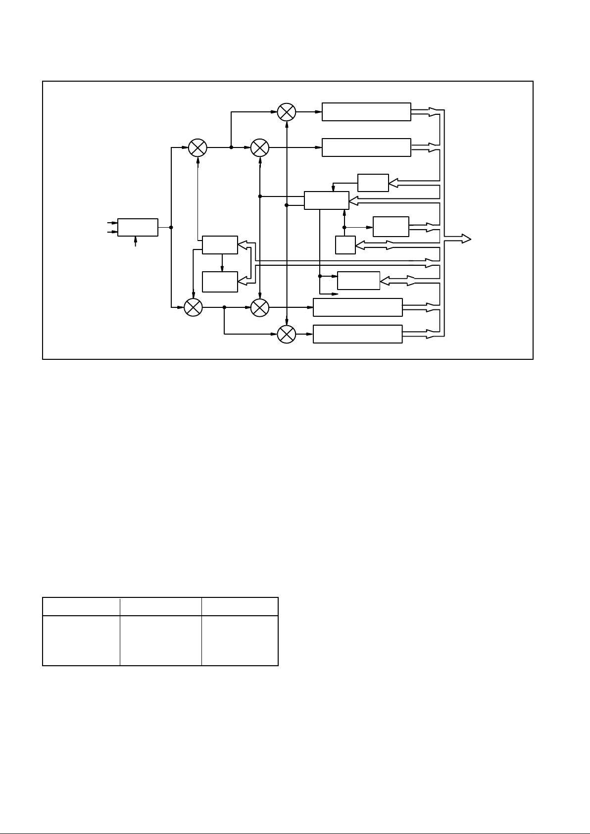
Fig. 4 shows a block diagram of the correlator. It consists
of the following blocks:
Clock Generator
The Clock Generator block divides the frequency of the
master clock CLK_T/CLK_I by 6 or 7 to give the internal multi–
phase set of clocks. When in Real_Input mode CLK_T/CLK_I
will normally be a 40MHz clock, which is divided by 7. When
in Complex_Input mode it will normally be at 35MHz which is
divided by 6. The SAMPCLK pin is an output giving a 4:3
mark–to–space ratio clock at 40 MHz / 7 (= 5·714MHz) in
Real_Input Mode.
The Clock Generator also produces the MICRO_CLK
signal at half the master clock frequency (20 MHz for
Real_Input mode, 17.5 MHz for Complex_Input mode) with a
1:1 mark–to–space ratio. This signal is output on the
MICRO_CLK pin in Standard Interface mode. However, its
main purpose is that of a synchronising clock to the memory
control logic in ARM System Mode and it is from this that the
processor clock output, MCLK, is derived.
Timebase Generator
The Timebase Generator produces 4 important timing
signals: ACCUM_INT, TIC, MEAS_INT and TIMEMARK.
ACCUM_INT is an interrupt provided to control data transfer
between the correlator accumulators and the microprocessor.
It may be detected by means of the ACCUM_INT output or by
reading the ACCUM_STATUS_A register (where bit 15 is a
flag indicating that ACCUM_INT has occurred since the
previous read of this register). ACCUM_INT is cleared by
reading ACCUM_STATUS_A.
After power–up this interrupt occurs every 505.05µs. Its
period can subsequently be changed in one of 3 ways:
1) toggling the FRONT_END_MODE bit of the
SYSTEM_SETUP register,
2) toggling the INTERRUPT_PERIOD bit of the
SYSTEM_SETUP register, or
3) writing directly to the PROG_ACCUM_INT register.
See section ‘‘Detailed Description of Registers” on page 25 for
more information.
TIC is an internal signal with a default period of
99999.90µs. It is used to latch measurement data (Epoch
count, Code phase, Code DCO phase, Carrier DCO phase
Fig. 4 Correlator block diagram
and Carrier cycle count) of all 12 channels at the same instant.
Its period can subsequently be changed, by writing to the
PROG_TIC_HIGH and PROG_TIC_LOW registers, or
toggling the FRONT_END_MODE bit of the
SYSTEM_SETUP register.
MEAS_INT is a signal derived from the TIC counter. It may
be used by the microprocessor as a software module
switching interrupt either by using the MEAS_INT output or by
reading the ACCUM_STATUS_B or MEAS_STATUS_A
register. MEAS_INT is activated at each TIC and 50 ms before
each TIC so long as the TIC period is greater than 50 ms. If the
TIC period is less than 50 ms, MEAS_INT is activated only at
each TIC. It is cleared by reading either the
ACCUM_STATUS_B or MEAS_STATUS_A register,
depending upon the MEAS_INT_SOURCE bit of the
SYSTEM_SETUP register.
TIMEMARK is also derived from TIC and may be output on
one of the discrete output pins. This signal is intended to be
used as an accurate 1 Pulse Per Second timing reference,
aligned to UTC (Universal Time Co–ordinated system), with a
pulse width of 1ms.
TIMEMARK has two methods of operation but in both
TRACKING
MODULE
CHANNEL 0
TRACKING
MODULE
CHANNEL 1
TRACKING
MODULE
CHANNEL 2
TRACKING
MODULE
CHANNEL 3
TRACKING
MODULE
CHANNEL 11
REGISTER
SELECTS
ADDRESS
DECODER
A<9:2>
32 BIT BUS
D<15:0>
CONTROL
BUS
INTERFACE
STATUS
REGISTERS
SYSTEM STATUS
MULTI–
PHASE
CLOCKS
CLOCK
GENERATOR
CLK_T
CLK_I
SAMPCLK
MICRO_CLK
MEAS_INT
ACCUM_INT
TIMEBASE
GENERATOR
TIC
INTERNAL
SAMPCLK
LATCHED
SIGN0 & MAG0
LATCHED
SIGN1 & MAG1
SAMPLE
LATCH
SIGN0 &
MAG0
SIGN1 &
MAG1
V
DD
POWER SUPPLY
V
SS
BITS

9
GP2021
cases TIMEMARK rising edges are generated co–incident
with the rising edges of TIC. Therefore, for TIMEMARK to be
aligned with UTC, TIC must be aligned with UTC. This is done
by modifying the TIC period for a single TIC cycle, then setting
it back to its original value, thus slewing the phase of TIC.
TIMEMARK may be generated by setting the
TIMEMARK_ARM bit in the TIMEMARK_CONTROL register,
in which case the next TIC will generate a rising edge at
TIMEMARK and clear the TIMEMARK_ARM bit. Alternatively
TIMEMARK may be generated as a programmable integer
number of TIC’s, again under the control of the
TIMEMARK_CONTROL register.
Status Registers
There are four status registers (ACCUM_STATUS_A, _B,
_C and MEAS_STATUS_A). These contain flags associated
with the accumulated and measurement data held on each of
the 12 channels. Some system level status bits also appear in
these registers.
Sample Latches
The Sample Latches synchronise data from the front end
to the internal SAMPCLK. In Real_Input mode the down
converted satellite signal can be sampled at the output of the
front end by SAMPCLK. This data is then input to the GP2021
as 2 bit data on either the SIGN0, MAG0, or SIGN1, MAG1
inputs, where it is re–sampled at the next rising edge of
SAMPCLK. These signals are then distributed to the 12
tracking modules.
When a GP2015 or GP2010 front end is used, the data
represents a band–limited signal at an IF centered on
4.309MHz. Sampling at 5.714MHz aliases it to an IF of
1.405MHz.
In Complex_Input mode, the down converted satellite
signal is applied direct to the GP2021 at its SIGN0, MAG0,
SIGN1, MAG1 inputs, which act as In–Phase Sign, In–Phase
Magnitude, Quadrature Sign and Quadrature Magnitude
respectively. These signals are sampled at 5.833MHz within
the correlator and then passed to the tracking modules.
Address Decoder
The Address Decoder performs address decoding for the
correlator.
Bus Interface
The Bus Interface controls the transfer of data between the
external 16 bit wide data bus and the internal 32 bit data bus.
Apart from the code and carrier DCO increment values, all
data transfers are 16 bits wide. Write operations to the code
and carrier DCO’s are 32 bit data transfers, in which the High
16 bit word must be written immediately before the low 16 bit
word. Note that the write cycle to write cycle delay of 300 ns
referred to in the Microprocessor Interface does not apply
between the first and second write cycles for 32 bit DCO data
transfers. For further information see the Microprocessor
Interface section.
TRACKING MODULES
The Tracking Modules are 12 identical signal tracking
channels numbered CH0 to CH11, each with the block
diagram shown in Fig 5. These blocks generate the data used
to track the satellite signals. There is no overwrite protection
mechanism on this data. For further information see the
section on CONTROLLING THE GP2021.
Each Tracking Channel can be individually programmed to
operate in either Update or Preset mode. Update mode is the
normal mode of operation. Preset mode is a special mode of
operation where writes to certain registers are delayed until
the next TIC to allow synchronisation of registers and
presetting of the code DCO phase. For further information see
the Preset Mode section in the Detailed Operation of the
GP2021.
The individual sub–blocks in the tracking modules are:
Carrier DCO
The Carrier DCO, which is clocked at the SAMPCLK
frequency, is used to synthesise the digital local oscillator
signal required to bring the input signal to baseband in the
mixer block, and must be adjusted away from its nominal value
to allow for Doppler shift and reference frequency error.
When used with the GP2015/GP2010 the nominal
frequency of this signal is 1·405396825 MHz (with a resolution
of 42.57475 MHz) and is set by loading the 26 bit register
CHx_CARRIER_DCO_INCR. This very fine resolution is
needed so that the DCO will stay in phase with the satellite
signal for an adequate time. The Carrier DCO Phase cannot
be directly set, but must be adjusted by altering the frequency.
The Carrier DCO outputs are 4 level, 8 phase sinusoidals
with the following sequences over one cycle:
As the clock to the DCO is normally less than 8 times the
output frequency, not all phases are generated in every cycle.
With a typical clock frequency of 5·714 MHz and an output
frequency of 1·405 MHz there are only around 4 phases per
cycle. These will slide through the cycle as time progresses to
cover all values.
Code DCO
The Code DCO is similar to the Carrier DCO block. It is also
clocked at the SAMPCLK frequency and synthesises the
oscillator required to drive the code generator at twice the
required chipping rate. The nominal frequency of the output is
2·046 MHz, to give a chip rate of 1·023 MHz and is set by
loading the 25 bit register CHx_CODE_DCO_INCR.
It is programmed with a resolution of 85·14949 mHz when
used with a GP2015/GP2010 front end. The very fine
resolution is again needed to keep the DCO in phase with the
satellite signal. The Code DCO Phase can only be set to the
exact satellite phase in Preset mode. In Update mode, it must
be aligned with the satellite phase by adjusting its frequency.
Carrier Cycle Counter
The Carrier Cycle Counter is 20 bits long, and keeps a
count of the number of cycles of the Carrier DCO between
TIC’s. This is not needed for a basic navigation system but
may be used to measure the range change (delta–range) to
each satellite between TIC’s. The delta ranges can be used to
smooth the code pseudo–ranges. For finer detail the Carrier
DCO phase may also be read at each TIC to give the fractional
part of the cycle count or delta–range.
C/A Code Generator
The C/A Code Generator generates the selected Gold
code for a GPS satellite (1 to 32), a ground transmitter
(pseudolite, 33 to 37), an INMARSAT–GIC satellite (201 to
211) or a GLONASS satellite. A Gold code is selected by
writing a specific pattern of 10 bits, as listed in the section
‘Detailed Description of Registers’, to the CHx_SATCNTL
register, or by setting the GPS_NGLON bit to Low for the
GLONASS code. Two outputs are generated to give both a
PROMPT and a TRACKING signal. The TRACKING signal
can be set to one of four modes: EARLY (one half chip before
the PROMPT signal), LATE (one half chip behind),
DITHERED (toggled between EARLY and LATE every 20ms)
or EARLY–MINUS–LATE (the signed difference).
The output code is a sequence of +1’s and –1’s for all code
types except EARLY–MINUS–LATE where the result can also
Destination Arm
I
LO
Q
LO
Sequence
–1+1+2+2+1–1–2–2
+2+2+1–1–2–2–1+1
Table 1 Carrier DCO outputs
10
GP2021
be a 0. To avoid having an unused LSB in the accumulators,
the values in EARLY–MINUS–LATE mode are halved from
the +2, 0, –2 that results from the calculation (+1 or –1) – (+1
or –1) to +1, 0, –1. This must be considered when choosing
thresholds in the software, as the correlation results will be
exactly half of the values otherwise expected.
At the end of every code sequence (1023 chips in GPS
mode or 511 chips in GLONASS mode) a DUMP signal is
generated to latch the Accumulated Data for use by the signal
tracking software. Each channel is latched separately, as the
satellite signals are not received in phase with each other.
Source Selector
In Real_Input mode the Source Selector selects which
input signal pair to use (SIGN0/MAG0 or SIGN1/MAG1). In
Complex_Input mode SIGN0/MAG0 are passed to the In–
phase arm and SIGN1/MAG1 to the Quadrature arm. The data
is treated as having the values shown in Table 2 below (in both
modes):
Carrier Mixers
The Carrier Mixers multiply the digital input signal by the
Carrier DCO digital local oscillator to generate a signal at
baseband. In Real_Input mode both I and Q Carrier DCO
phases are directed to the appropriate mixers. In
Complex_Input mode a single In–Phase Carrier DCO output
is used in both mixers since the input signal is already in I and
16 BIT ACCUMULATE
AND DUMP – Q_TRACKING
16 BIT ACCUMULATE
AND DUMP – Q_PROMPT
CODE
SLEW
C/A CODE
GENERATOR
CODE
PHASE
COUNTER
CODE
DCO
EPOCH
COUNTERS
DUMP
ACCUMS, CODE PHASE, ETC
16 BIT ACCUMULATE
AND DUMP – I_PROMPT
16 BIT ACCUMULATE
AND DUMP – I_TRACKING
CARRIER
CYCLE
COUNTER
CARRIER
DCO
I
1,
2
SOURCE
SELECTOR
SIGN 0
AND
MAG 0
SIGN 1
AND
MAG 1
SELECT
SOURCE
AND
SELECT
MODE
IN AND OUT
DATA
BUSSES
CODE
MIXER
CARRIER
MIXER
1, 2,
3, 6
3
LO
Q
LO
I
LO
1
1, 0
OR
1,
Fig.5 Tracking Module block diagram
Sig
0
0
1
1
Mag
1
0
0
1
Value
-3
-1
+1
+3
Table 2 SIGN/MAG values
Q form. The mixing of the Carrier DCO outputs with the input
signal produces a baseband signal which can have the values
±1, ±2, ±3 and ±6.
Code Mixers
The Code Mixers multiply the I and Q baseband signals
from the Carrier Mixers with both the PROMPT and
TRACKING local replica codes to produce 4 separate
correlation results. The correlation results are passed to the
Accumulate and Dump blocks for integration.
Accumulate and Dump
The Accumulate and Dump blocks integrate the Mixer
outputs over a complete code period of nominally 1ms.
There are 4 separate 16 bit accumulators for each channel.
These represent the correlation of the I and Q signals with the
PROMPT and TRACKING codes, over the integration period.
There is no overwrite protection mechanism on these
registers so the data must be read before the next DUMP.
Code Phase Counter
The Code Phase Counter counts the number of half–chips
of generated code and stores this value in the
CHx_CODE_PHASE register on each TIC.
Code Slew Counter
The Code Slew Counter is used to slew the generated code
by a number of half chips in the range 0 to 2047. In Update
mode the slew occurs following the next DUMP. In preset
mode it occurs at the next TIC. All slew operations are relative
to the current code phase. The Code Slew counter must be
written to each time a slew is required.
During the slewing process the accumulators for the
channel being slewed are inhibited so that the first result is
valid. If a slew is written while a channel is disabled it will occur
as soon as the channel is enabled.

11
GP2021
Epoch Counter
The Epoch Counters keep track of the number of code
periods over a 1 second interval. This is represented by a 5 bit
word for the number of 1 ms integration periods (0 to 19), plus
a 6 bit word containing the number of 20 ms counts (0 to 49).
The Epoch Counters can be pre–loaded to synchronise them
to the data stream coming from the satellite. This value will be
transferred immediately to the counter when in Update mode,
or after the next TIC if in PRESET Mode.
The Epoch Counter values are latched on each TIC into the
CHx_EPOCH register. In addition the instantaneous values
are available from the CHx_EPOCH_CHECK register.
PERIPHERAL FUNCTIONS
The following section describes the Dual UART, Real
Time Clock and Watchdog, Power and Reset Control and
Discrete I/O blocks.
Dual UART
A Dual UART is included for serial communications. It has
2 identical blocks, UART_A and UART_B, each containing
separate transmit and receive channels. The parity and
separate transmit and receive baud rate can be configured
independently for each UART. Each uses a polled processor
interface and each transmit and receive channel has an 8 byte
deep FIFO.
For further information on the UART registers refer to the
Detailed Description of Registers and the GP2021 Register
Map.
A typical serial data stream is shown in Fig. 6. The Parity
bit is optional and if no parity is selected the time slot for it is
removed from the data stream and the Stop bit follows
immediately after the last data bit in both transmit and receive
directions. Note that the LSB is always preceded by a Start bit.
Table 3 shows possible UART configurations.
Last
Start D8 D9 D10 D11 D12
D13 D14
D15
P
Stop
First
LSB MSB Parity
(optional)
Fig. 6 Serial Data waveform
Parameter Value
Start bits 1 bit Low
Data bits 8 bits Logic 0 = Low
Logic 1 = High
Stop bits 1 bit High
Parity Odd/Even/None
Flow control None
Transmit FIFO depth 8 bytes
Receive FIFO depth 8 bytes
FIFO speed Transmit FIFO write rate and Receive FIFO read rate maximum is one byte per 230ns.
The maximum buffer through delay is 2 µ s.
Data rate 300, 600,1.2k, 2.4k, 4.8k, 9.6k, 19.2k, 38.4k and 76.8k baud. Transmit and Receive
rates individu-ally configured.
Table 3 UART Functionality
Receiver
The incoming data streams on RXA, RXB are sampled by
a clock at nominally 20 times the data rate, to search for an
incoming Start bit. Once the receiver is synchronised to the
data stream, each data bit is sampled only at its nominal centre
to avoid errors due to slow or noisy bit edges. The receiver will
resynchronise to each Start bit to prevent the accumulation of
phase errors.
Only valid data (having correct Start, Stop and Parity bits)
will be stored in the receiver FIFO. If a received word contains
a parity or framing (Start/Stop bit) error, the appropriate flag bit
will be set in the status register. If too many valid data words
are received for the FIFO to hold, the excess will not be written
into the FIFO, and an Overflow bit will be set in the status
register. When receiving a continuous transmission, the Start
bit of one word will follow immediately after the Stop bit of the
preceding word. At lower word rates, a High is expected
between words. The receiver will accept data with a baud rate
error of up to ±1%.
Transmitter
Data is transmitted on pins TXA and TXB. In continuous
transmission, the Start bit of one word will follow immediately
after the Stop bit of the preceding word. At lower word rates,
a High is sent between words.
If too many data words are written by the microprocessor
to the UART for the transmitter FIFO to hold, the excess will not
be stored. The UART will resume normal operation as soon as
space becomes available. To avoid data loss, the software
should limit the transmit data rate by either: keeping track of
the number of bytes sent and the time to transmit them, or
should read the Status register and stop writing when the Full
bit is set.
12
GP2021
Reset
It is possible for the software to reset either UART
independently via the RESET_CHx registers. A hardware
reset affects both UARTs. During a UART reset, the contents
of all Control, and Status registers will be cleared. In addition
the Transmit and Receive FIFO’s will be emptied and the TX
outputs will be held Low.
Channel Loopback
For system test purposes, a loopback facility is provided
for each channel, controlled by the Configuration registers. In
loopback, the TX output is set High.
Real Time Clock (RTC) and Watchdog
This block consists of a 32.768kHz crystal oscillator, a
fixed divider, a 24 bit counter, a Watchdog function and three
8 bit data registers. XIN and XOUT are the crystal in and
crystal out connections to the oscillator circuit. A recommended crystal oscillator circuit is shown in Fig. 7. When the
Real Time Clock SSis not being used, XIN must be tied Low.
The first divider is a fixed divide by 32768 giving a 1 Hz
output. The counter then counts seconds, giving a maximum
time of 194 days. The time is output in three 8 bit registers with
the data being latched when a read is performed to the LS
register (The register holding the least significant byte of the
clock data). On reaching its maximum count, the count is
frozen (i.e. all 1’s), until being reset.
In Power Down mode the Real Time Clock continues to
run, but access to the data registers is not allowed. When
normal power is restored, the software can determine the
elapsed time whilst in Power Down mode, thereby assisting in
estimating the current position of GPS satellites and so
reducingTime–To–First–Fix.
The Watchdog generates a System Reset (see Power And
Reset Control) if the Watchdog Reset address has not been
written to for a period of approximately 2s. The watchdog
function is inhibited whilst in Power Down mode and can be
disabled via a bit in the System Configuration register.The
software is able to reset the Real Time Clock and Watchdog
via the Clock Reset and Watchdog Reset registers
respectively. In addition the watchdog is reset during a System
Reset.
For further information on the registers refer to the section
Detailed Description of Registers.
Power and Reset Control
This block performs 2 functions: Power Control and
System
Reset Generation
Power Down Mode
In order to allow power conservation within a battery
backup system, the GP2021 provides a Power Down mode,
in which the supply voltage may drop to a minimum of 2.2V,
thereby minimising the supply current. In this mode all
functions within the GP2021 are disabled except for the Real
Time Clock.
The GP2021 is placed in Power Down mode by taking the
POWER_GOOD pin Low. In ARM System mode with the
NBRAM pin held Low, the initiation of Power Down mode is
delayed until just after a falling edge of MICRO_CLK so as not
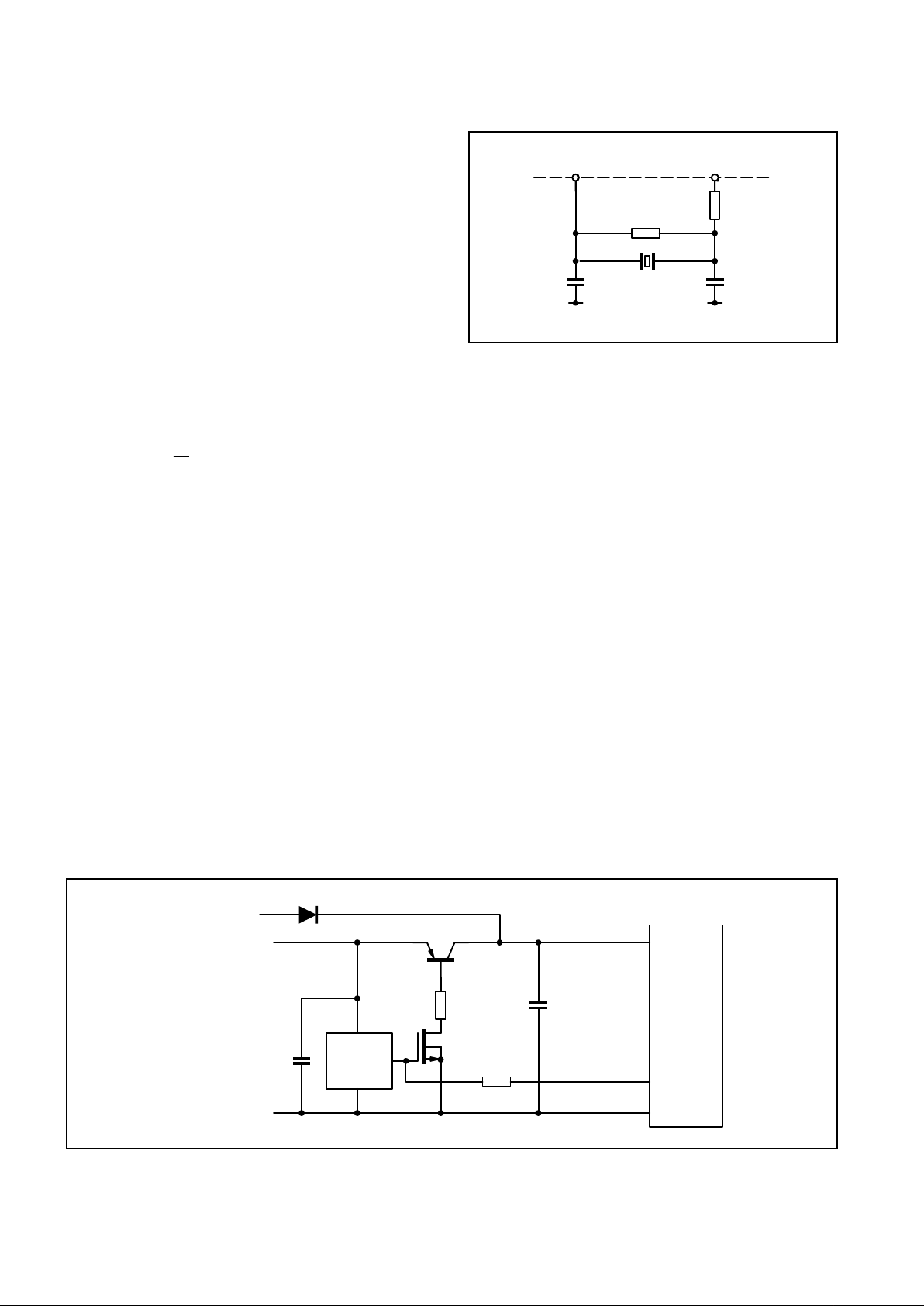
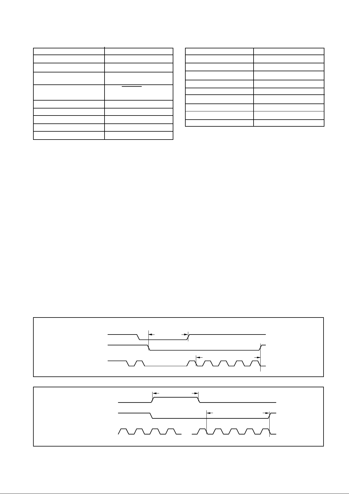
to corrupt battery backed RAM. Fig. 8 shows a suggested
circuit implementation. Table 4 shows output logic levels in
Power Down mode.
In Power Down mode all inputs and I/Os except
POWER_GOOD and XIN are internally switched to known
logic levels to prevent extraneous switching from causing
excessive power consumption, and may therefore be left
floating. All the I/O pins (D<15:0>, MULTI_FN_IO and
DISCIO) have their output drivers driven to the High
Impedance state.
XIN
XOUT
22pF22pF
CRYSTAL
10M
V
SS
V
SS
680k
32.768kHz
Fig. 7 Recommended Crystal Oscillator Circuit
BATTERY
SUPPLY
D1
SUPPLY+5V
C1
VOLTAGE
SENSOR
GP2021
POWER_GOOD
C2
V
DD
T2
R1
R2
T1
V
SS
V
SS
Fig. 8 : Suggested Battery Backup Configuration
13
GP2021
Pin Name Logic Level
NW<3:0> / NC Low
NRD / NC Low
NRAM Low
(standard interface mode)
NRAM NB RAM
(ARM system mode)
NROM / NC High Impedance
NSPARE_CS/NC High Impedance
NEEPROM / NC High Impedance
TXA,TXB Low
ACCUM_INT High Impedance
Pin Name Logic Level
MEAS_INT High Impedance
A
BORT / MICRO_CLK Low
MCLK / NC Low
ARM_ALE / NC Low
DBE / NC Low
NRESET_OP Low
DISCOP High Impedance
SAMPCLK Low
XOUT Active
Table 4 : Output Logic Levels in Power Down Mode
Hardware Reset Generation
The manner in which a hardware reset occurs depends on
whether the GP2021 is in ARM System mode or Standard
Interface mode. During a hardware reset, the NRESET_OP
pin is taken Low and the reset signal is applied within the
GP2021 to all blocks except the Real Time Clock.
There are 3 sources of hardware resets common to both
ARM System and Standard Interface modes, with an
additional source in Standard Interface mode:
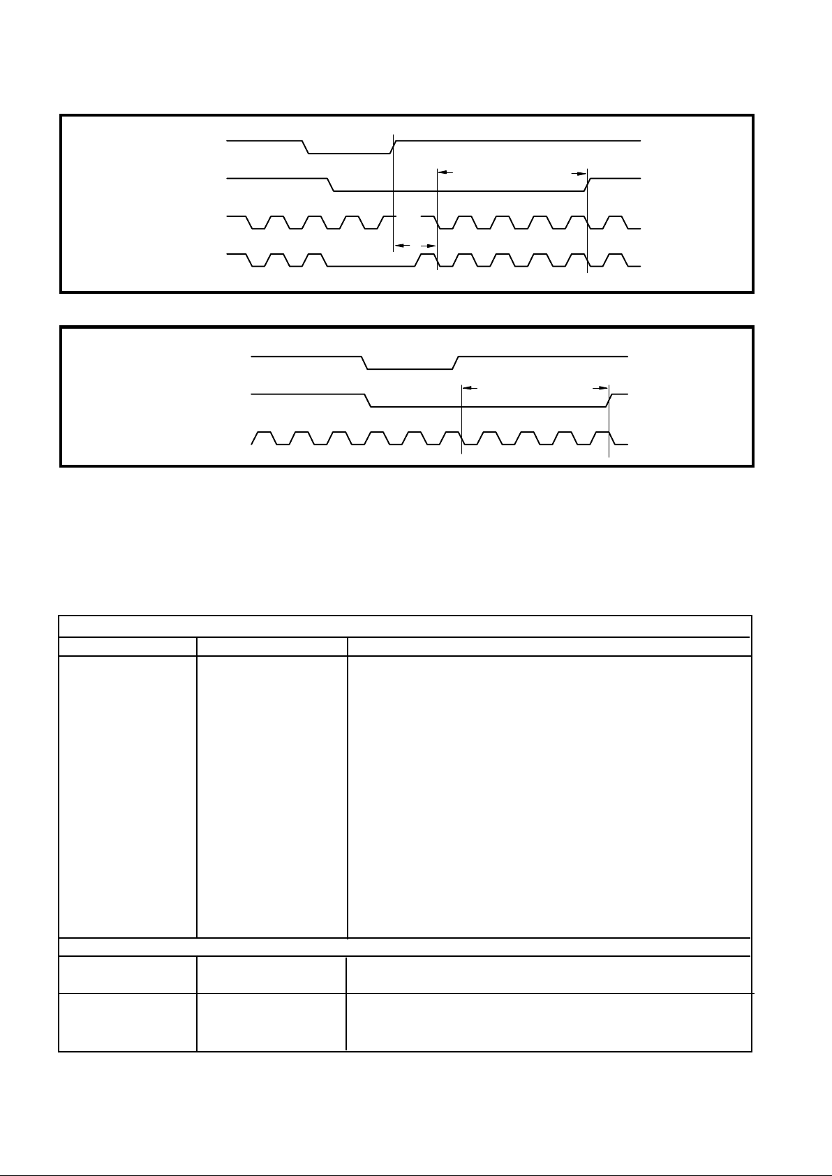
POWER_GOOD: A hardware reset will occur if this pin is
taken Low, as shown in Fig. 9. The purpose of this input is to
detect a power failure. If the NBRAM pin is held Low in ARM
System mode, the internal Power Down mode is not entered
until about 6ns after the falling edge of MICRO_CLK,
otherwise it is entered immediately. This allows for RAM write
cycles to complete sensibly when Battery Backed–Up RAM is
used, with no corruption of RAM data.
Watchdog: An expiry of the watchdog will result in a
hardware reset as shown in Fig. 10. This reset will clear the
watchdog whose time–out period is 2–3 seconds.
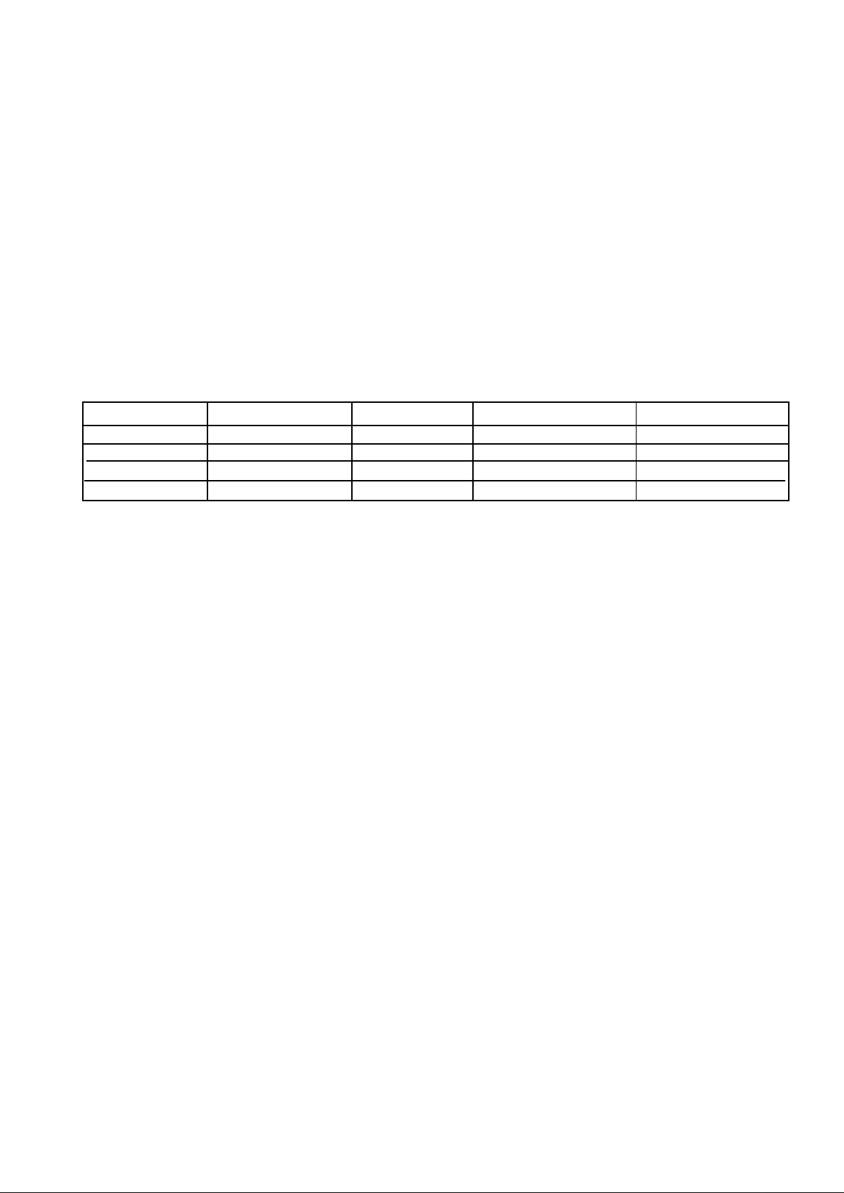
PLL_LOCK: The PLL_LOCK pin is used to indicate (when
High),that the phase locked loop in the RF front end, which
generates the master clock, is in lock. This signal is filtered
within the GP2021 and the reset state associated with it is only
de–activated if the PLL_LOCK input has been high for
approximately 50 ms as shown in Fig. 11.
NRESET_IP: In addition to the 3 reset sources described
above, an active Low NRESET_IP pin is available in Standard
Interface mode if the system resets are to be generated
externally. Fig. 12 shows a NRESET_IP generated reset.
Note that the NRESET_OP pin will go High 4 MICRO_CLK
cycles after all hardware reset sources have cleared. This
fulfills the reset requirements of the ARM60 microprocessor.
For information on the state of the registers following a
hardware reset refer to the Detailed Description of Registers
section.
System Error Status Register
This allows the software to determine whether the source
of a hardware reset was from a power failure, a PLL_LOCK
failure, watchdog timeout or from an external reset in Standard
Interface mode. For further information refer to the Detailed
Description of Registers section.
MICRO_CLK/
NRESET_OP
POWER_GOOD
4 CYCLES
MCLK
Power Down Mode
Fig. 9 : POWER_GOOD Hardware Reset Generation (NARMSYS = ‘0’, NBRAM =‘0’)
MICRO_CLK/
NRESET_OP
WATCHDOG
122 s
4 CYCLES
MCLK
Fig. 10 : Watchdog Hardware Reset Genera-
14
GP2021
PLL_LOCK
NRESET_OP
MICRO_CLK
4 CYCLES
MCLK
50ms
NRESET_IP
NRESET_OP
MICRO_CLK
4 CYCLES
Fig. 11 : PLL_LOCK Hardware Reset Generation
Fig. 12 : NRESET_IP Hardware Reset Generation
Discrete I/O
The GP2021 contains a number of pins which may be used
as discrete inputs or discrete outputs for general purpose
system monitoring and control applications. The actual pins
which may be used for each function vary according to the
application and the interface mode of the GP2021.Table 5
shows a list of possible discrete inputs and outputs and the
modes in which they may be used. The level on all discrete
inputs can be read from the IO_CONFIG register. The status
of the DISCIP pin may also be read from
ACCUM_STATUS_B. The discrete outputs are controlled via
either the SYSTEM_SETUP or IO_CONFIG registers.
Discrete Inputs
Pin Name Read Location Conditions for use as Discrete Input
NRW/DISCIP3 IO_CONFIG Standard Interface mode.
NOPC/NINTELMOT IO_CONFIG ARM System mode (debug disabled).
NMREQ/DISCIP2 IO_CONFIG Standard Interface mode.
NBW/WRPROG IO_CONFIG Motorola mode only.
DISCIO IO_CONFIG DISCIO configured as discrete Input.
NBRAM/DISCIP4 IO_CONFIG Standard Interface Mode.
MULTI_FN_IO IO_CONFIG MULTI_FN_IO configured as discrete input.
SIGN0, MAG0 IO_CONFIG Single real input mode (GP2010 or GP2015) front end using
SIGN0, MAG0.
SIGN1, MAG1 IO_CONFIG Single real input mode (GP2010 or GP2015) front end using
SIGN1, MAG1.
DISCIP1 IO_CONFIG Always available – dedicated Discrete Input.
ACCUM_STATUS_B
RXA IO_CONFIG UART Channel A not used.
RXB IO_CONFIG UART Channel B not used.
Discrete Outputs
Pin Name Configuration Possible Outputs
Location
DISCOP SYSTEM_SET_UP High, Low, CH0 Dump, TIMEMARK, 100kHz Square Wave, Scan Out.
DISCIO IO_CONFIG High, Low, TIMEMARK, 100kHz Square Wave.
MULTI_FN_IO IO_CONFIG High, Low, TIMEMARK, 100kHz Square Wave.
Table 5 : Discrete Input/Output Configuration
15
GP2021
Digital System Test Interface
The GP2021 contains a Digital System Test mode to allow
testing of the digital section of the system board. Provided that
the MULTI_FN_IO pin is High, this mode is enabled
subsequent to a hardware reset or a write of specific data to
the IO_CONFIG register. The enabling of Digital System Test
mode has 3 effects:
(1) The master clock inputs, CLK_T and CLK_I, are
replaced by the signal on the RXA pin. This allows the GP2021
to be clocked synchronously with the board tester which is
relevant in ARM System mode where the GP2021 produces
the main processor clock to the ARM60.
(2) The RXB pin becomes the active High RTC Reset
input. This is mainly intended for factory testing of the
GP2021, allowing the RTC to be reset on power up, but may
also be used to disable the RTC and Watchdog circuits in this
mode.
(3) The PLL_LOCK input and its associated 50ms delay as
a reset source is overridden. This removes the dependency
on the presence of the front end circuit.
MICROPROCESSOR INTERFACE
The Microprocessor Interface of the GP2021 is compatible
with most 16 and 32 bit microprocessors. It can be configured
for either ARM System mode or Standard Interface mode by
means of the NARMSYS pin.
In Standard Interface mode, two mode control pins
NINTELMOT and WRPROG are provided. NINTELMOT
selects between Intel and Motorola style interfaces, with
WRPROG selecting either Intel i486 or 80186 style interfaces.
See Table 6 for more details.
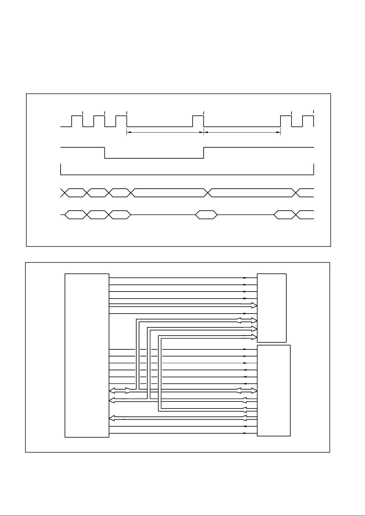
NARMSYS NINTELMOT WRPROG Mode Processor
0 x x ARM System ARM60
1 1 x Standard Interface Motorola style
1 0 0 Standard Interface Intel 80186 style
1 0 1 Standard Interface Intel 486 style
Table 6 Microprocessor Interface Configuration.
General Interface Timing
In addition to the detailed timings associated with
individual read and write cycles ( see Electrical Characteristics
section), the internal architecture of the correlator also
imposes limits on cycle to cycle timings (in particular write to
write cycle and write to read cycle). For a simple
microprocessor interface, it must be ensured that no attempts
are made to access the correlator for the 300ns following the
end of a correlator write cycle in Real_Input mode, or 314ns in
Complex_Input mode. However, if the controlling software is
to be allowed to write rapidly to the correlator (e.g. block
writes), then a more complex bus interface (which inserts wait
states) will be required. Note that this limitation only applies
after correlator writes, not peripheral function writes, and also
does not apply to writes to the correlator X_DCO_INCR_HIGH
address.
The correlator section of the GP2021 uses a multi–phase
clock internally, and the correlator registers load on specific
clock phases. At the end of a write cycle, the falling edge of the
internal write strobe latches both the relevant address and
data bits. This data is then loaded from the internal data bus
to the relevant register at some time during the following 300ns
for Real_Input mode or 314ns for Complex_Input mode. A
write cycle to the Correlator with no writes in the preceding
300ns (314ns) may be performed immediately, so long as the
detailed signal timings are met. However, subsequent read or
write cycles to the Correlator after this write cycle may need to
be delayed if they would modify the internal address or data
lines. Correlator read cycles with no write cycles in the
preceding 300ns (314ns) are self–contained, and do not delay
subsequent cycles. An isolated read cycle requires only
sufficient wait states to meet the detailed signal timings.
Write Cycle To Read Cycle Timings
As described previously, the internal write cycle of the
Correlator takes 300ns (314ns). Only once the write cycle is
complete will the correlator address decoders switch to
decoding the current address. The correlator uses a pre–
charged internal data out bus and hence the decoded address
lines must be stable before the internal bus drivers are
enabled (when the read strobe goes high). Consequently, the
read strobe must be held Low until some time after the end of
the 300ns (314ns) internal write cycle, to allow sufficient
internal address setup time. For the exact timing requirements
see the Electrical Characteristics Section.
Write Cycle To Write Cycle Timings
The internal write cycle of the correlator takes 300ns
(314ns) after the falling edge of the write strobe. During this
time the write internal address and data busses (latched by
write) must not be modified. If a second write follows the first,
the second write cycle must be delayed such that it ends no
earlier than 300ns (314ns) after the end of the previous write.
The ‘end’ being a falling edge on the internal write strobe. The
specific interface signal timings must also be met.
Notes about Interface Timing Constraints
It should also be noted that these timings need only be met
for correlator accesses, not support function accesses, since
these utilise self–contained write cycles and are not clocked
by the multi–phase clocks. In addition, writes to the Correlator
register X_DCO_INCR_HIGH need not incur subsequent
delays since writes to this location do not instigate an internal
write cycle. A write to this address must always be followed by
a write to either a CHX_CARRIER_DCO_INCR_LOW or a
CHX_CODE_DCO_INCR_LOW register and it is this second
associated write which instigates the internal write cycle.
In ARM System mode all these timing requirements are
handled by the internal memory manager.
16
GP2021
WREN
READ
NCS
A<9:2>
D<15:0>
Read Read
Read
Write
Delayed W
rite
Delayed Read
NOTE: OP
and IP
are with respect to the GP2021. OP denotes a GP2021 Output, IP
denotes a processor output.
OP OP IP OP OPIP
300ns (314ns) 300ns (314ns)
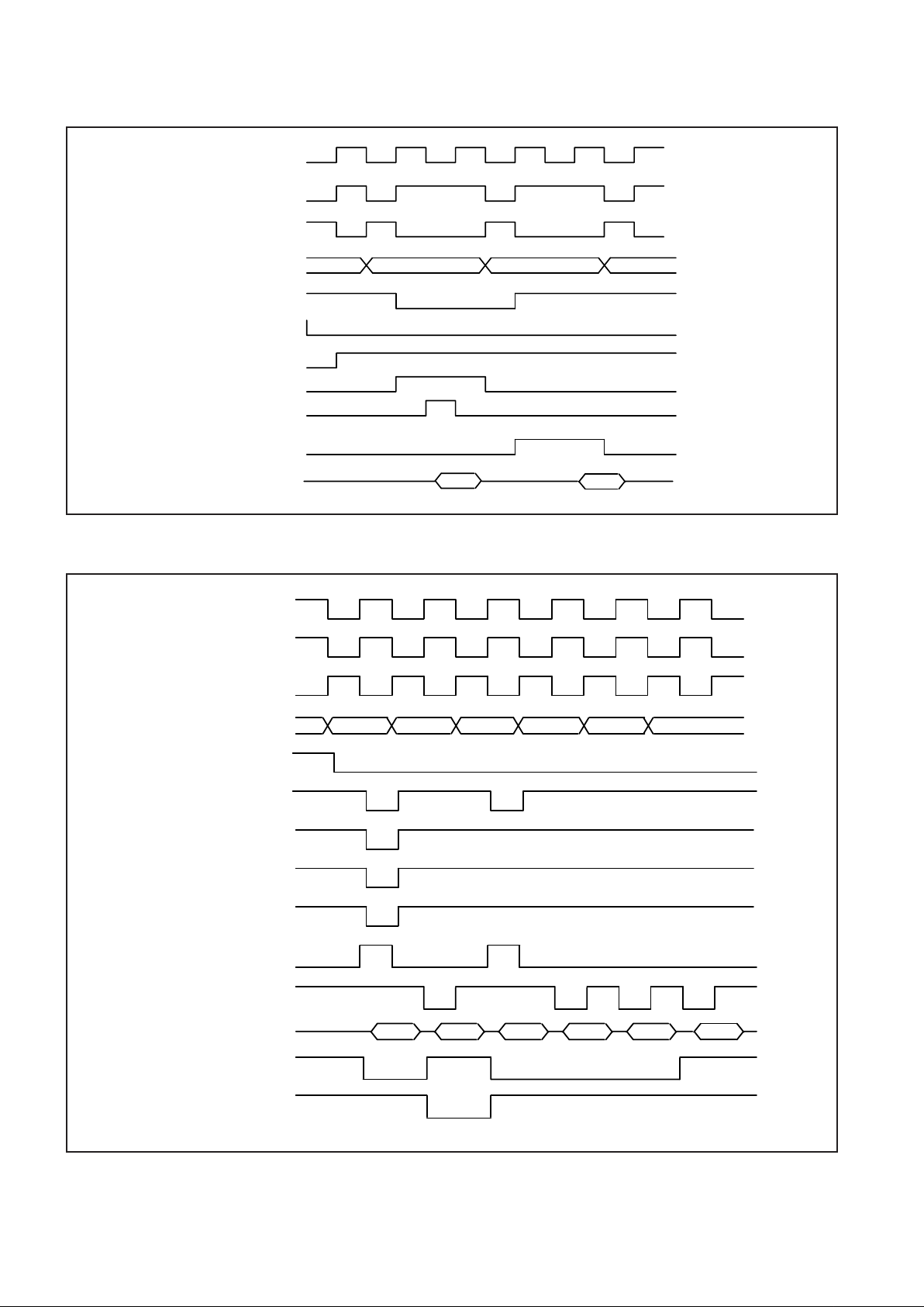
Fig.13 Correlator Bus Timing - Write to Write and Write to Read Timings
ARM60
GP2021
Memory
NRAM
NROM
NEEPROM
NSPARE_CS
NW<3:0>
NRD
D<15:0>
A<9:2>
A<19:10>
DBE
ARM_ALE
MCLK
NRW
NMREQ
NBW
D<15:0>
A<9:2>
A<22:20>,
A<1:0>
NOPC
ABORT
A<19:10>
(NRESET_OP
,
ACCUM_INT and MEAS_INT not shown)
Fig.14 ARM System Mode
Note that the exact number of wait states which need to be
inserted after a correlator write is not fixed. If the processor
were to perform a correlator write then spend 400ns
accessing a different peripheral, subsequent correlator reads
and writes would incur no additional delay. It is anticipated
that correlator wait states will be generated by either one or
two external counters, preset on the falling edge of a correlator
write, and which then count down to zero. Only once the
counter has reached zero may the next correlator access
either complete (write) or start (read).
A series of correlator reads and writes are shown in Fig.13.
17
GP2021
ARM System Mode
ARM System Mode, as shown in Fig 14, allows the
GP2021 to be interfaced with an ARM60 microprocessor and
external memory devices (i.e RAM, ROM, EEPROM,
EPROM, Flash) without the need for external glue logic.
Address Map
Both the GP2021 and external memory devices are
memory mapped into 1 Mbyte segments by A<22:20> as
shown in Table 7.
Decoded
A22 A21 A20 Device selected output
pin
0 0 0 ROM NROM
0 0 1 RAM NRAM
0 1 0 Correlator
0 1 1 Support functions
1 0 0 EEPROM NEEPROM
1 0 1 User defined NSPARE_CS
1 1 0 Not Decoded
1 1 1 Not Decoded
Table 7 ARM system map
Control Signals
The GP2021 uses the ARM60 control signals NBW,
NMREQ and NRW to generate the processor clock MCLK and
the control signals ARM_ALE and DBE to match the timing
requirements of the various memory devices .
The memory interface is via the memory chip select lines
( NRAM, NEEPROM, NROM and NSPARE_CS) , the Read
line (NRD) and the byte write select outputs ( NW<3:0> ).
ARM System Timing
The GP2021 timing diagrams for each of the memory
interfaces ( EEPROM, RAM, ROM, SPARE), and ARM60
areshown in the section Electrical Characteristics.
Wait State Generation
To allow access to slow peripherals or memory, the clock
(MCLK) to the ARM60 microprocessor may be stretched in
either Phase 1 (Low) or Phase 2 (High), thus allowing wait
states to be introduced (where a wait state is defined as being
one MCLK period long).
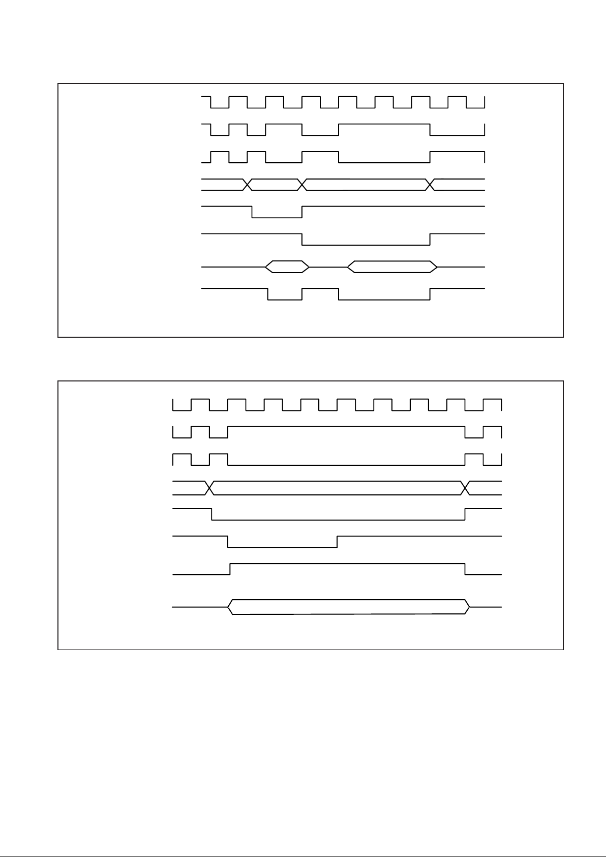
The GP2021 introduces one wait state for accesses to the
Real Time Clock, Dual UART and System Control registers,
as shown in Fig 15. Correlator accesses, as shown in Fig 19
incur one wait state; subsequent accesses being prevented
from contravening the Correlator requirements (see
Correlator Functional Description) by adding several wait
states.
In order to ensure compatibility with variety of memory
devices, the ROM interface is programmable with between
one to three wait states, while the EEPROM and SPARE
interfaces can be programmed with between three to six wait
states via the Wait State Register. For further information on
the Wait State Register, refer to Detailed Description of
Registers. Read and write cycles for the RAM, EEPROM (or
Spare) and ROM interfaces are shown in Figs 16–18.
During a read cycle from Flash Memory, the output disable
to data bus release time, could be greater than 25 ns. Hence
in order to avoid bus contention, the nominal period of MCLK
is stretched by 25 ns during the following cycle.
The ARM60 is able to perform either byte or word ( 4 bytes
wide) writes to memory. All registers within the GP2021 are
word aligned, with only write accesses to external RAM being
either byte or word aligned. The signal NBW is used to indicate
either a byte or word write request, with A<1:0> performing
byte selection.
Decoding of NBW and A<1:0> is performed by the
Microprocessor Interface, with NW<3:0> being the byte write
select outputs to memory. During a word write all four of the
outputs NW<3:0> will be active.
Note that the register addresses for the Correlator and
Support Functions are as shown in the GP2021 Register Map.
18
GP2021
Fig.15 Peripheral functions write/read Cycle
Fig.16 RAM read/write Cycle
20MHz
INTERNAL
MCLK
ARM_ALE
NRW
NMREQ
NBW
DBE
INTERNAL
WRITE
INTERNAL
READ
D<15:0>
VALID
1 W
AIT ST
ATE
VALID
CLOCK
A<22:20>,
A<9:0>
MCLK
NOTE: This diagram assumes NMREQ is Low
.
20MHz
INTERNAL
ARM_ALE
NRAM
NW0
NW3
NW2
NW1
D<15:0>
DBE
NRD
NRW
NBW
VALID VALID VALID VALID VALID
CLOCK
A<22:20>,
A<9:2>
VALID
19
GP2021
Fig.17 ROM (1 wait state) and EEPROM/spare (2+1wait states) Read Cycles
MCLK
NOTE: NRW, NMREQ and DBE are assumed to be Low
20MHz
INTERNAL
CLOCK
ARM_ALE
NEEPROM
NROM
NRD
D<15:0>
A<22:20>,
A<9:0>
Fig.18 EEPROM (or Spare) Write Cycle
MCLK
NOTE: NBW and NR
W are assumed to be High for this cycle
20MHz
INTERNAL
CLOCK
ARM_ALE
A<22:20>,
A<9:0>
NEEPROM
NW<3:0>
DBE
D<15:0>
 Loading...