MITEL DES9208901DGAZ, DES9208901AC Datasheet

1
SP8782A & B
SP8782A & B
1GHz ÷ 16/17, ÷32/33 Multi-Modulus Divider
Description
The SP8782 is a multi-modulus divider which divides by 16/
17 when the Ratio Select input is low and by 32/33 when
theRatio Select input is high. When high, the modulus Control
input selects the lower division ratio (16 or 32) and the higher
ratio (17 or 33) when it is low.
The device uses resynchronisation techniques to reduce the
effects of propagation delays in frequency synthesis.
The SP8782A (ceramic DIL package) is characterised over
the full military temperature range of -55°C to +125°C, the
SP8782B (miniature plastic DIL package) over the industrial
range of -40°C to+85°C.
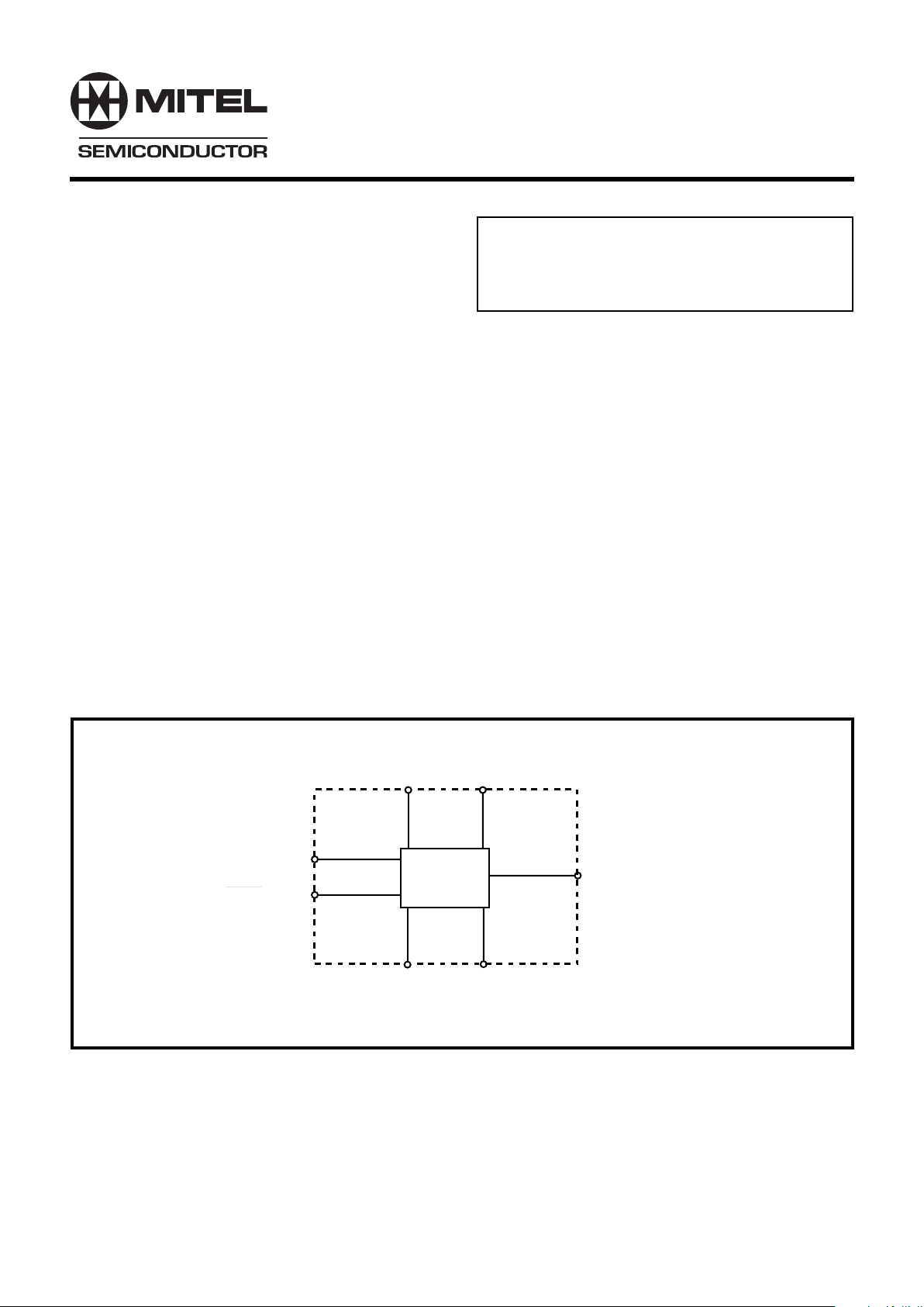
Figure 1 Functional Diagram
Features
● Advanced Resynchronisation techniques to negate
loop delay effects
● CMOS compataible output capability
● Multi-Modulus division
● Available as DESC SMD 5962-9208901MPA
Odering Information
SP8782 A DG
SP8782 B MP
DES9208901/AC/DGAZ(SMD)
DS3651 Issue 2.4 June 1999
Absolute Maximum Ratings
Supply Voltage 6V
Clock input level 2.5V p-p
Junction temperature +175°C
Storage temperature range:
SP8782A -55°C to +150°C
SP8782B -55°C to +125°C
V
RATIO
SELECT
CC
MODULUS
CONTROL
INPUT
CLOCK INPUT
CLOCK INPUT
OUTPUT
V
EE
1
2
2
3
4
5
7
÷ 16/17
÷ 32/33

2
SP8782A & B
Electrical Characteristics
Unless otherwise stated, the Electrical Characteristics are guaranteed over the specified supply, frequency and
temperature range.
Supply Voltage, VCC = +4V to +5.5V, VEE = 0V
Temperature T
amb
= -55°C to +125°C, (SP8782A), -40°C to +85° C (SP8782B)
Characteristic Pin Value Conditions
Min Max Units
Maximum frequency 2, 3 1 GHz Input = 200-1200mVp-p
(sinewave input)
Minimum frequency 2, 3 50 MHz Input = 400-1200mVp-p
Min Slew rate for low frequency operation 2, 3 100 V/µs
Power Supply current, I
CC
8 60 mA Output unloaded, VCC=5.5V
Output low voltage 7 0 1.7 V
Output high voltage 7 V
CC
-1.4 V
CC
V
Modulus control input high voltage 5 0.7V
CC
V
CC
V At driver end of 3kΩ resistor
Modulus control input low voltage 5 0 0.3V
CC
V At driver end of 3kΩ resistor
Modulus control input high current 5 0.6 1.2 mA Via 3kΩ resistor to V
CC
Modulus control input low current 5 -0.6 -1.2 mA Via 3kΩ resistor to V
CC
Ratio select input high voltage 1 0.6V
CC
V
CC
V
Ratio selected input low voltage 1 0 0.4V
CC
V
Ratio select input current 1 -10 10 µA
Clock to output propagation Delay 2,3,7 3 ns
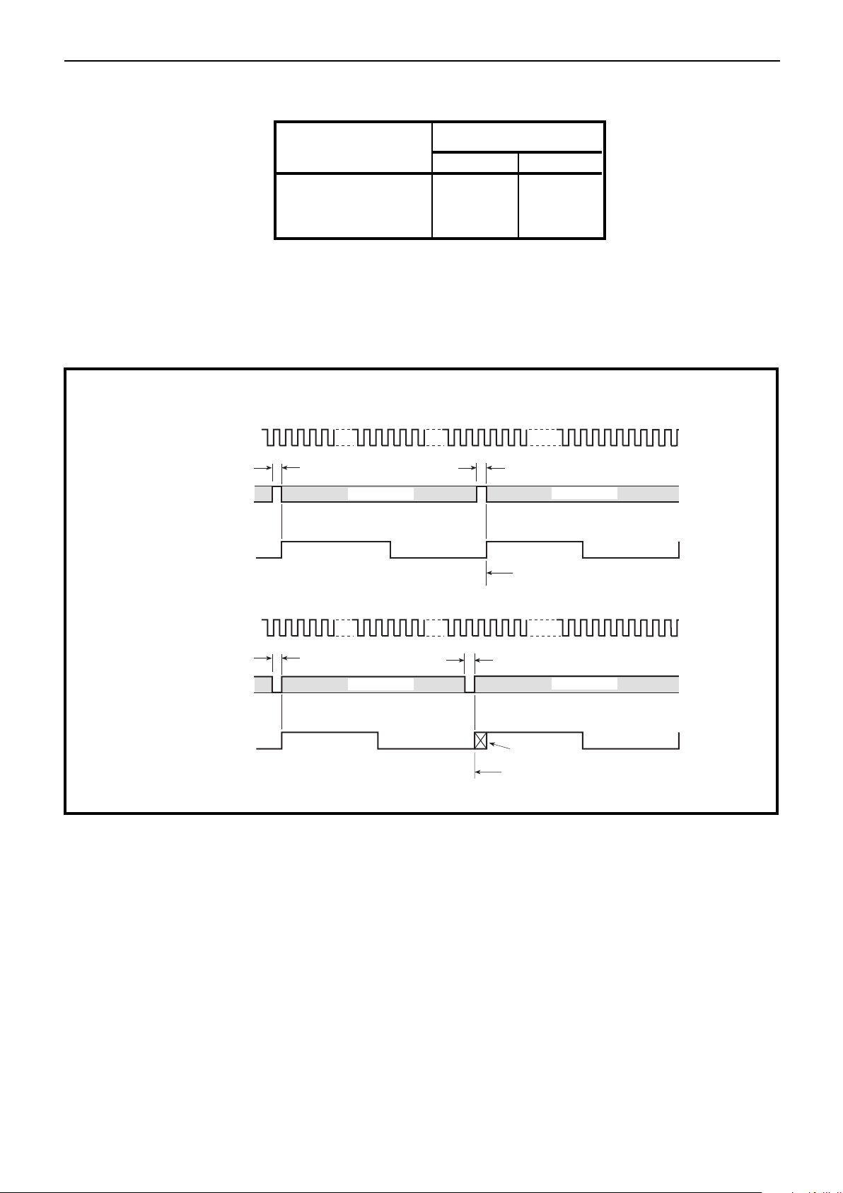
Set-up time, t
s
5,7 3 ns See note 1 and Fig. 3a
Release time,t
r
5,7 3 ns See note 2 and Fig. 3b
Notes: 1. The set-up time ts is defined as the minimum time that can elapse between L→H transition of the
modulus control input and the next L→H output transition to ensure that the ÷ 16 (32) mode is obtained.
2. The release time tr is defined as the minimum time that can elapse between H→L transition of the modulus
control input and the next L→H output transition to ensure that the ÷ 17 (33) mode is obtained.
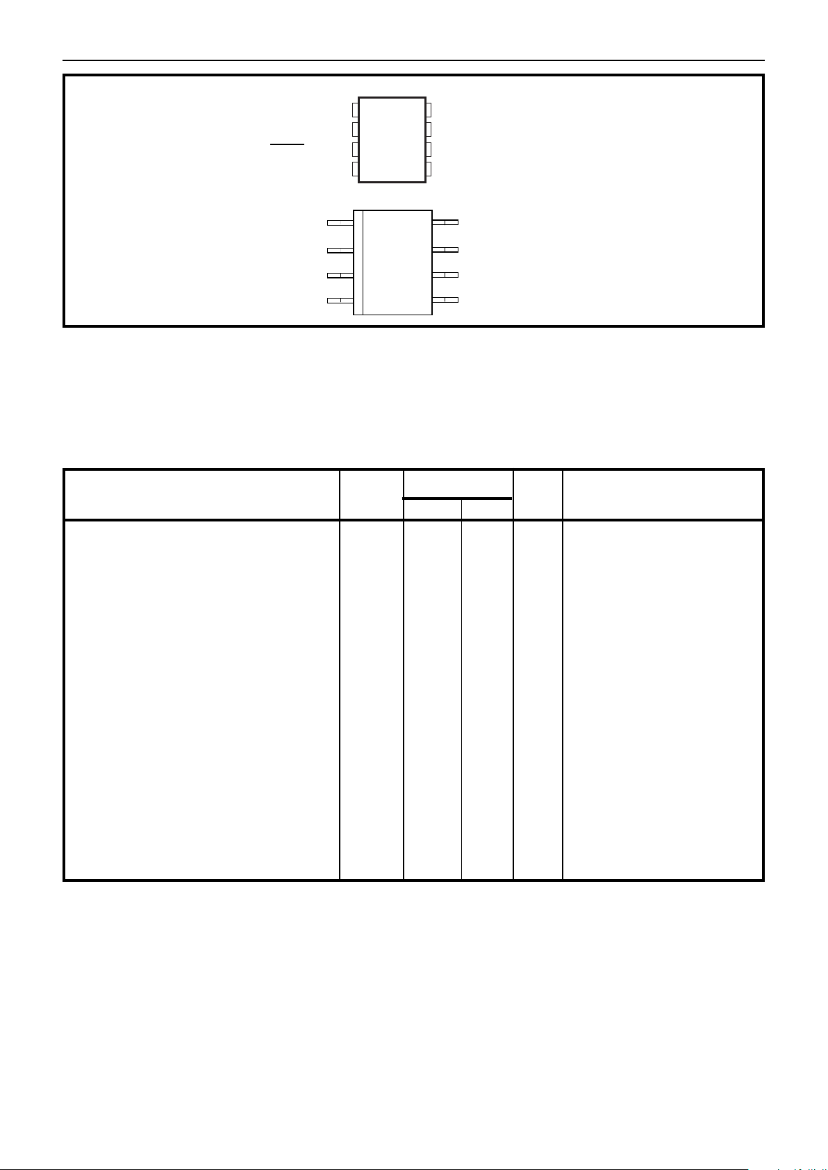
Figure 2 Typical Pin Connections
DG 8
RATIO SELECT
CLOCK INPUT
CLOCK INPUT
V
EE
V
CC
OUTPUT
NC
MODULUS CONTROL
1
2
3
4
8
7
6
5
MP 8
V
CC
OUTPUT
NC
MODULUS CONTROL
1
2
3
4
8
7
6
5
RATIO SELECT
CLOCK INPUT
CLOCK INPUT
V
EE

3
SP8782A & B
DON’T CARE
8 (16)
t
r
t
r
8 (16)
9 (17)
CLOCK INPUT
MODULUS
CONTROL INPUT
OUTPUT
DON’T CARE
8 (16)
DIVIDE-BY-17 (33) MODE
ESTABLISHED
EXTRA
PULSE
Fig. 3a Setting divide-by-16 (32) mode
DON’T CARE
9 (17)
t
s
t
s
8 (16)
8 (16)
CLOCK INPUT
MODULUS
CONTROL INPUT
OUTPUT
DON’T CARE
8 (16)
DIVIDE-BY-16 (32) MODE
ESTABLISHED
Figure 3 Timing diagrams
Table 1 Truth table for control inputs
Modulus control Ratio select input
input 01
0 ÷17 ÷33
1 ÷16 ÷32
Figure 3b Setting divide - by - 17 (33 mode)
Figure 3a Setting divide - by - 16 (32 mode)
 Loading...