MITEL DES9056701DGAZ, DES9056701AC Datasheet

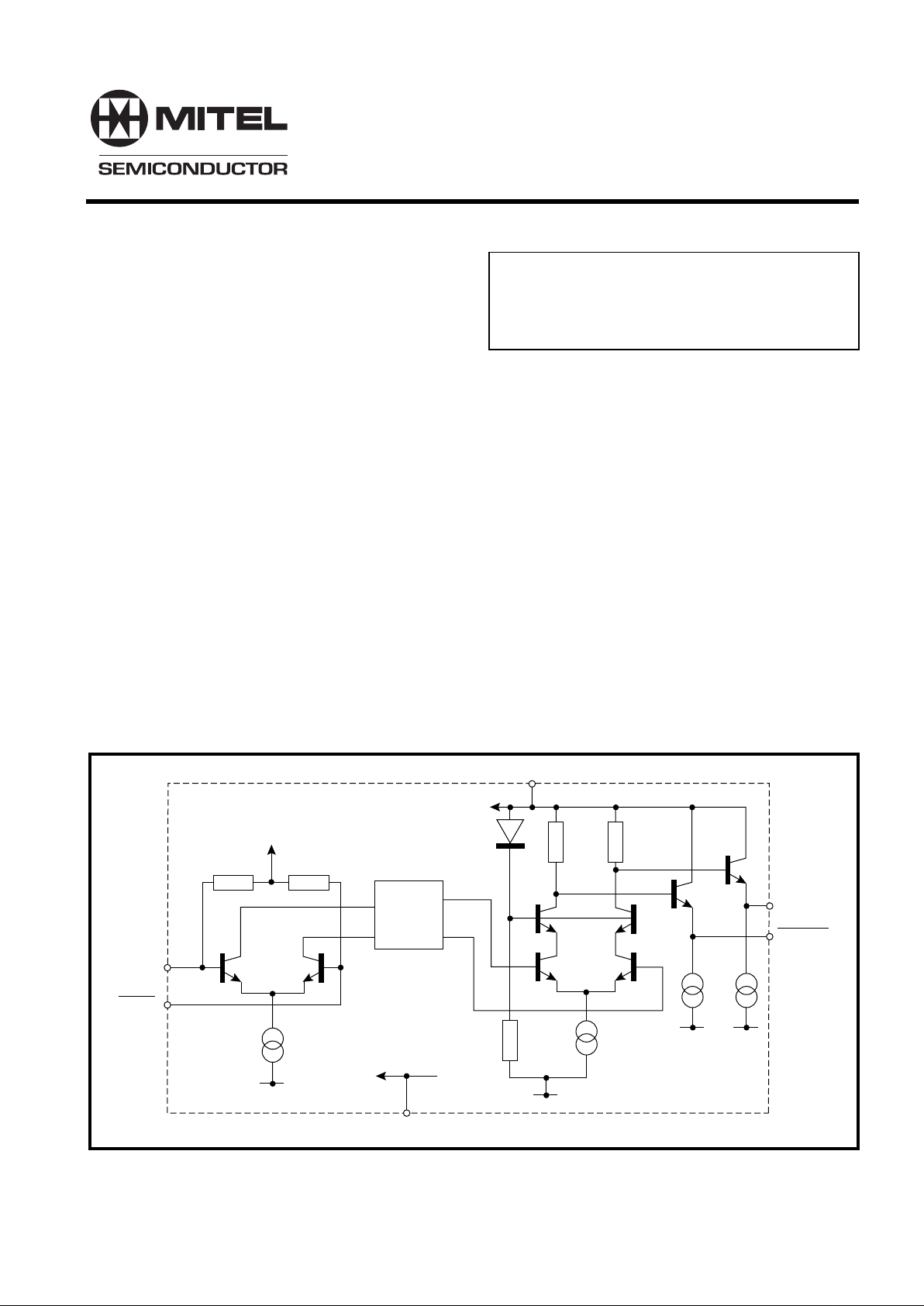
The SP8804 is one of a range of very high speed low
power prescalers for professional and military
applications. The device features a complementary
output stage with on chip current source for the emitter
follower outputs.
Figure 1 SP8804 Block diagram
400 400
500
500
÷4
2mA
5mA
6
7
6.75mA
5
3
2
VCC
1
SUPPLY
INPUT
INPUT
GND
OUTPUT
OUTPUT
V
REF
(2V)
Ordering Information
SP8804/A/DG Military temperature range
DES9056701/AC/DGAZ (SMD)
SP8804
3.3GHz ÷ 4 fixed Modulus Divider
Advance Information
DS2112 Issue 7.3 June 1999
Description
Thermal Characteristics
θja = 150°C/W
θjc = 50°C/W
Absolute Maximum Ratings
Supply voltage V
CC
6.5V
Clock Input voltage 2.5V p-p
Storage temperature range -65°C to +150°C
Junction temperature +175°C
Features
● Very High Speed Operation 3.3GHz
● Silicon Technology for low Phase Noise
(Typically better than -140dBc/Hz at 10kHz)
● Specified Over the Full Military Temperature
Range
● Low Power Dissipation 370mW (typ)
● 5V Single Supply Operation
● High Input Sensitivity
● Very Wide Operating Frequency Range
● Available as DESC SMD 5962-9056701MPA

SP8804 Advance Information
2
Electrical Characteristics
Guaranteed over the temperature range T
amb
-55°C to +125°C (see note) and supply voltage range 4.75V
to 5.25V. Tested at T
amb
= -55°C and +105°C, VCC = 4.75V and 5.25V.
Supply current
Input sensitivity
0.65GHz to 2.8GHz
3.3GHz
Input impedance
(series equivalent)
Output Voltage with fin =1000MHz
Output Voltage with fin = 3GHz
1
2, 3
2, 3
6, 7
6, 7
0.8
74
50
2
1
0.25
mA
mV
mV
Ω
pF
Vp-p
Vp-p
90
175
400
VCC = 5V
RMS sinewave
measured in 50 ohm system.
See Figs. 3 & 4
VCC = 5V
VCC = 5V load as Fig. 4
Pin
Characteristic
Conditions
Min Typ Max
Units
Value
NOTE: Devices must be used with a suitable heatsink to maintain chip temperature below 175°C when operating
at T
amb
>105°C.
500
400
300
200
100
VIN (mV RMS
INTO 50 OHMS)
1 2 3 4
,,
FREQUENCY (GHz)
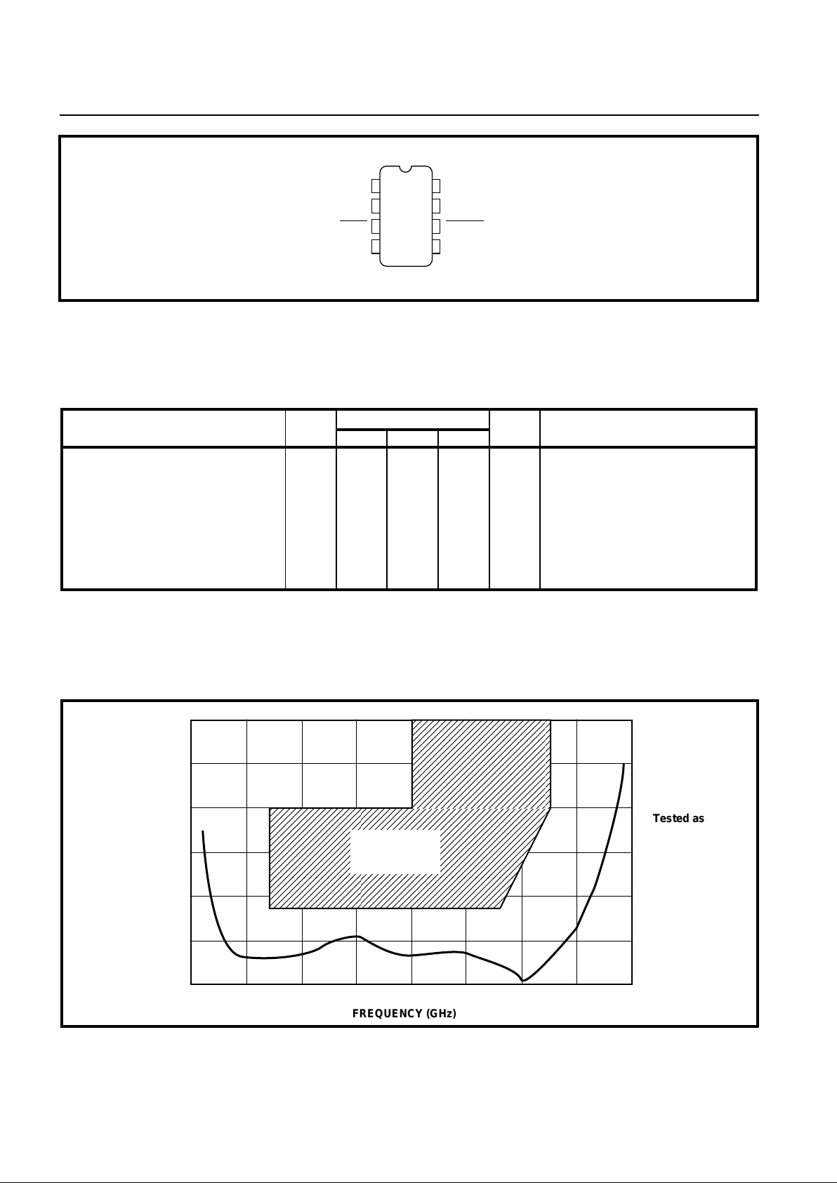
Tested as
specified in Table
of electrical
characteristics
*
GUARANTEED*
OPERATING
WINDOW
Figure 3 Typical input sensitivity
DG8
Figure 2 Pin connections
NC GND
INPUT OUTPUT
INPUT OUTPUT
V
CC
5
6
7
8NC
4
3
2
1
SP8804
 Loading...