

Page 1

(2786)A 1
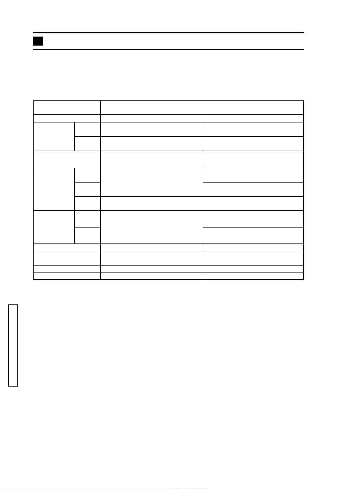
TROUBLESHOOTING CHART
This section consists of the following items.
CONTENTS -------------------------------------------------------------------------------------------------------------------Page
■Precautions --------------------------------------------------------------------------------------------------------------------- 1
■Control Switches --------------------------------------------------------------------------------------------------------------- 2
(1) Control Switches Location ----------------------------------------------------------------------------------------------- 2
(2) Control Switches Functions --------------------------------------------------------------------------------------------- 2
■Block Diagram ----------------------------------------------------------------------------------------------------------------- 3
■Circuit Board Connection Diagram --------------------------------------------------------------------------------------- 4
■Map of Electrical Elements -------------------------------------------------------------------------------------------------- 5
(1) CP-1 Compl PWB (#0408) ------------------------------------------------------------------------------------------------ 5
(2) PW-1 Compl PWB (#0432/-090,-0100,-300,-600)(0452/-090,-630,-650) ------------------------------------------ 6
(3) ST-1 Compl PWB (#0406) ------------------------------------------------------------------------------------------------ 6
(4) ST-2 Compl PWB (#0409) ------------------------------------------------------------------------------------------------ 6
■■
■Precautions
■■
(1)To check voltage, use digital Multimeter or an apparatus which input impedance of 10MΩ or greater.
(2)To check conductivity, use a circuit tester of 3V or less.
(3)Check mainly soldering at lead wires or electrical elements and switch operation, since elements (IC,
diode, transistor, resistor, or condenser) seldom cause the trouble.
(4)When checking, do not push elements or pull lead wires strongly.
(5)When checking voltage at patterns where switch operates, be careful not to prevent switch operation or
to scratch patterns.
(6)Before removing electrical parts, be sure to disconnect Power Supply.
(7)Before soldering, heat the soldering iron to 290 - 340℃. If higher, solder quickly.
(8)When handling ICs avoid static electricity.
TROUBLE-SHOOTING CHART
Page 2
2 (2786)A
Control Switches
(1) Control Switches Location
All control switches are equal in function switches and buttons on the exterior of the camera.
See pg. 2 of the check list in this manual.
(2) Control Switch Function
Names of Switch /
Button
Main switch
Shutterrelease button
S1
S2
Mode dial
Up
Controller
(Up/Down
Down
key)
Center
Controller
Left
(Left/Right
key)
Right
Menu button
Quick View/Delete
button
Display button
Flash-mode button
Function Operation
Activates/deactivates camera. On by pressing Main switch
Starts AE, AF and AWB.
Starts shutter release.
Selects recording, playaback,
movie/audio, or setup mode.
Zooms the lens.
Enlarges the image in playback mode.
Selects the menu to adjust.
Swiches AF area, or sets the options in
the menu.
Selects the frame in playback mode and
the menu to adjust.
In recording mode: Set functions selected
in the key customizing
Selects the menu On/Off. On by pressing Menu button
Recording: Switches to QV display
Playback: Select an image to delete.
Selects the LCD monitor status. On by pressing Display button
Selects a flash mode. On by pressing Flash-mode button
On by pressing Shutter-release button
partway down
On by pressing Shutter-release button
all the way down
On by turning Mode dial
On by pushing key up
On by pushing key down
On by pushing Center button
On by pressing Left key
On by pressing Right key
On by pressing QV/Delete button
TROUBLE-SHOOTING CHART
*: The battery type detection switch is located in the batttery chamber, not on the exterior.
Page 3

MIC
(2786)A 3
SPEAKER
CCD BLOCK
IC903
4Mpixel
CCD
UNIT LENS
Focus
Zoom
Iris
Shutter
Electric
Flash
CP1 BLOCK
IC905
IC951
CDS
AGC
12bit A/D
Motor
Driver
IC103
128Mbit
SDRAM
16Mbit
Flash
AUDIO
Circuit
IC121
IC181
TG
SG
Processor
SDRAM
Flash
I/F
A/D
D/A
Signal
Controller
SRAM SRAM
IC101
System
ASIC
Data Bus(32bit/36MHz)
SRAM
SD
I/F
JPEG
CODEC
NTSC/PAL Y/C
Encoder
SRAM OSD
UART
SIO
USB
UART
PARAREL
PO
U
V
Y
C
4FSC
MIX
NTSC
14.318MHz
PAL
17.734MHz
CLK GEN.
72.MHz
Xtal
28.63636MHz
IC111
X1101
Video
USB
IC171
LCD
Driver
Monitor
Back Light
IC501
DC/DC
Converter
LCD
PW1 BLOCK
PUSH
SW
Lithium
Battery
DC Jack
TROUBLE-SHOOTING CHART
SD CARD
PUSH
SW
CONTROL PANEL BACK
MODE
SW
4MHz
IC301
8bit
CPU
Sub CLKMain CLK
32.768KHz
STROBO
Circuit
ST1
BLOCK
Page 4

4 (2786)A
BACK
FLASH
REFLECTOR
1
1111
W1600
W1500
W1400
XKT
XAN
TRG
GRAY
PINK
BLACK
AL5.0V
VCC
VCC
VCC
GND
GND
GND
ST1
RED
JW541
1
GND
BATTERY
RDY
TRIG
CHG
VMONIT
LED0(SELF)
AL3.2V
SCAN OUT3 SCAN OUT3
SI0
SI1
SI4
GRAY
JW542
1AV4J10QT401G
CN501
DC_IN
PW1
1AV4J10QS201G1AV4J11RX20BG
CN502CN541
2 30
3
4
5
6
7
8
9
10
11
12
13
14
15
16
17
18
19
20
2
3
4
5
6
7
8
9
10
11
12
13
14
15
16
17
18
19
20
STOPSTOP
AL5.0V
VCC
VCC
VCC
GND
GND
GND
GND
BATTERY
RDY
TRIG
CHG
VMONIT
LED0(SELF)
AL3.2V
SI0
SI1
SI4
P ON
P(A) ON
LCD ON
BL ON
+8.5V(L)
+1.8V(D)
+1.8V(D)
MGND
MGND
UNREG-M
UNREG-M
UNREG-SY
-7.6V(A)
+15.0V(A)
+3.3V(D)
+3.3V(D)
GND
GND
+5.0V(D)
+5.0V(A)
GND
GND
LED_CATHODE
LED_ANODE
TRIG
RDY
STOP
CHG
VMONIT
AL3.2V AL3.2V
LED0(SELF)
SCAN OUT3
SI0
SI1
SI4
BAT CHG
BAT DTC
BATTERY
GND
LIGHT
DATA0
DATA1
987654321
DATA2
121110
WP
CARD
COMMON
CP1
(DMA)
(SYA)
(CAA)
IRIS -
CN951
SHUTTER -
SHUTTER +
1AV4J11SL160G
IRIS +
ZOOM A+
ZOOM B+
ZOOM B-
ZOOM A-
987654321
COM
ZOOM SW
2
1
VDD
VSS
CLOCK
COMMAND
VSS
CN107
LED_ANODE
LED_CATHODE
1AV4J10QL020G
1AV4J11RX40AG 1AV4J11NR213G
40
39
38
37
36
35
34
33
32
31
29
28
27
26
25
24
23
22
21
20
19
18
17
16
15
14
13
12
11
10
9
8
7
6
5
4
3
2
1
CN104 CN108
40
DC_IN
39
P ON
38
P(A) ON
37
LCD ON
36
BL ON
35
+8.5V(L)
34
+1.8V(D)
33
+1.8V(D)
32
MGND
31 10
MGND SCAN IN2(A)
30
UNREG-M
29
UNREG-M
28
UNREG-SY
27
-7.6V(A)
26
+15.0V(A)
25
+3.3V(D)
24
+3.3V(D)
23
GND
22
GND
21
+5.0V(D)
20
+5.0V(A)
19
GND
18
GND
17
LED_CATHODE
16
LED_ANODE
15
TRIG
14
RDY
13
STOP
12
CHG
11
VMONIT
10
9
LED0(SELF)
8
SCAN OUT3
7
SI0
6
SI1
5
SI4
4
BAT CHG
3
BAT DTC
2
BATTERY
1
GND
DATA3
CN143
1AV4J11B5970G
FOCUS A-
FOCUS A+
FOCUS B-
16151413121110
PL ANO
PL COL
FOCUS B+
MICLENSSD
2
1
GND
MIC
CN181
1AV4J10QL020G
SCAN OUT 2
SCAN IN0(C)
SCAN IN4(C)
SCAN IN1(C)
SCAN IN2(C)
AL3.2V
VFLED(G)
VFLED(R)
SCAN IN0(A)
SCAN IN1(A)
SCAN OUT 0
SCAN IN3(A)
SCAN OUT 1
SCAN IN3(B)
SCAN IN1(B)
SCAN IN4(B)
SCAN IN0(B)
SCAN IN2(B)
SP+
SP-
1AV4J11B5510G
CN110
GND
USB D-
USB VDD
USB D+
AVJACK
A OUT
V OUT
GND
1
2
3
4
5
6
7
8
9
11
12
13
14
15
16
17
18
19
20
21
1
2
3
4
5
6
7
8
FPC
USB
1AV4J11B2720N
1
11
JW551
JW552
RED
GRAY
BAT +
1
JW501
BAT -
1
JW502
TROUBLE-SHOOTING CHART
ST2
JK501
DC JACK
TERMINAL CHARGE
1AG2TEF0151--
JK502
CRADLE JACK
1
3
2
1
3
2
BNCG
-7V(A)
CN901
+15V(A)
+15V(A)
1AV4J11RX24BG
1
432
1
GND
-7V(A)
432
SUBGT
V5BV6V5A
98765
98765
V4
GND
GND
CCDOUT
GND
V1
V2
V3A
V3B
SUB
H1
RG
GND
GND
H2
242322212019181716151413121110
242322212019181716151413121110
COM
CKV1
CN171
1AV4J11SL240G
242322212019181716151413121110
CKV2
STV
XSTV
VVDD
ENB
XENB
CSV
VBB
DSG
DSD
XDSG
R
STH
VSS
CSH
XSTH
HVDD
987654321
CKH1
CKH2
W1-63000/SX741-JM
LCD
H1
CN931
+15V(A)
+15V(A)
GNDV6V5A
-7V(A)
-7V(A)
SUBGT
V5B
V1
GND
CCDOUT
GND
V2
V3A
SUBRGGND
V3B
V4
GND
GND
H2
CCD
Page 5

(2786)A 5
C9507
C9508
C1806
R1806
R1807
C1807
X3001
R9501
R9502
1
C9513
C9514
R9513
Q9503
R9507
R9508
R1819
R1818
R1809
7
8
IC181
14
15
R1817
C1808
R1820
C1810
C1801
12
13
R9506
R9503
R9504
R9510
24
R9505
25
CN951
C9511
C9512
R9509
R9514
Q9502
C1912
D1001
Q1802
R1808
Q1801
C1818
C1805
C1804
21
R1803
R1824
C1811
C1821
R1811
C1825
IC951
C9509
C9510
L9002
R9016
+
1
R1802
28
C1816
C1815
22
C1814
C1813
R1810
C1824
C1711
C1819
C1823
R1814
R1815
COM
1
36
16
Q9504
IC191
C1911
+
RB102
C9040
C9045
D9001
14
C9010
R9004
R9003
C1066
C1048
C1061
C1063
CL411
24
48
C9506
L1903
C9503
C9505
C9504
37
C1201
R1005
C1910
RB101
13
IC904
C9005
C1053
R1071
R1073
R1037
R1036
R1006
C1067
C1701
R1703
R1711
SIDE-B
SX741_CP1
6
CN302
JSEL
5
R1063
ZFRD
L1201
XF121
C1072
C9502
R1201
IC121
R1008
R1009
C1065
R1012
RB105
R1011
RB104
RB103
1
26
C9006
XF902
C9046
Q1051
C1057
R1052
R1051
C1055
C1054
C1051
R1057
C1052
C1050
R1053
R1712C1056
CN171
R1713
R1701
10
1
ZFWR
C1026 C1028 C1073 C1070
TP301
VDD
1.8
GND
IC103
IC101
R1007
C1046
R1054
15 11
C1101
L1102
R1103
L1103
R1104
IC111
20 16
R1102
L1101
C1114
1
C1312
R1350
C1311
R1359
R1311
1
C1058
XF111
Q1305
Q1705
C1757
R1734
C1702
D1701
1AG4B10E1700AB
TP302
TDI
TDO
R1055
VA131
VA132
TCK
C1032
X1101
C1103
Q1304
TRST
R1502C1076
C1044
R1705
C1703
R1709
C1753
C1718
R1003
Q1508
R1531
R1004
C1075
R1516
RB301
C1704
R1735
C1719
C1709
C1706
C1716
C1715
C1733
R1702
C1717
C1713
R1704
R1706
C1037
R1001
RB171
TMS
R1056
10
6
5
C1104
C1102
R1111
C1105
C1301
C1759
R1302
Q1301
R1301
R1731
R1738
R1732
R1733
C1758
VDD3
D1501
R1528
D3004
L1701
R1707
48
R1710
49
50
60
64
1
CN107
D3003
NTSC/PAL
VSS
CL410
CL415
B
CSYNC
CL416
CL412
Q1541
R1542 R1541
R1072
R1074
D3006
CN108
1
C1729
C1730 C1728
40
C1720
IC171
10
R1708
C1710
C1746
C1743
C1741
IC173
C1754
C1748
XENB
G
CL413
R
CL414
202
21
33
32
17
16
R3004
R1715
L1303
R1529
8
L1302
CN110
C1302
1
C1512
L1304
R1527
C1515
IC152
+
C1513
R1526
Q1504
R1513
L1502
C1508
Q1503
C1511
R1509
C1519
R1508
R1515
812
7
6
3
2
1
9
C2001
Q1501
C1502
Q1502
R1521
R1522
R1514
R1507
R1519
R1066
R1065
5
4
Q1507
R1510
R1512
R1511
R1523
R1064
R1062
R1061
R2033
C2002
R1530
L2001
11
CN143
L1040
C2015R2032
IC203
L1051
C1040
D2007
C2017
Q3006
Q2006
Q1431
RB141
R1435
L1702
C1705
C1779
21
R3032
+
R3034
CN104
40
Q3007
IC303
10
C3017
Q3003
R3018
R3015
R3003
R3016
10
R3017
R3002
R3005
C3005
C3004
C3006
1
4
SX741_CP1
IC308
5
8
C3003
R3006
1AG4B10E1700AB
R1014 R1013
C3009
C3008
SIDE-A
R9038
R9037
R9035
24
CN901
1
C9002
Q9003
Q1432
R1436R1434
R1431
R9012
C9001
R9014
C1778
20
C1030
C1039
C1042
R1601
C1034
R1901
R3031
R3030
VA301
1
64
1
C3030
16
17
RB302
D3002
13
Q3001
C3002
20
C9038
+
R1031
C9037
C3007
C9036
C9035
Q9001
R9005
C9003
R9001
60
20
R3012
C3010
Q3002
12
C9039
24
25
C9032
13
C9047
12
C9019
C9021
R9002
C1904
Q3005
IC301
C9031
R3033
10
IC905
C9028
C9029
C9030
C9033
+
IC909
XF901
C9020
R3022
R3028
R3035
R3025
32
30
L9001
1
36
C9034
C9027
C1812
1
2
CN181
R3024
Q3004
48
40
X3002
C3013
33
R9011
R3008
C3014
R9010
48
RB901
RB902
C9022
40
R9021
C9023
37
C1827
C1817
C1809
R1816
R1813
IC182
IC183
C1822
R3019
C1905
R1902
R3011
C3011
R3010
C3016
R3013
R3014
C3015
NTSC/PAL
R9022
C9025
R1812
TROUBLE-SHOOTING CHART
Page 6

6 (2786)A
11
C5061
R5106
R5103
C5103
R5105
20
10
21
L5007
CN501
C5012
C5002
C5014
13
C5037
C5006
D5011
L5005
40
R5093
C5093
R5095
C5001
R5006
12
R5067
1
R5114
+
Q5102
C5102
Q5101
R5111
R5117
-
R5118
R5115
L5015
L5010
Q5014
R5091
C5092
Q5015
R5023
D5012
R5092
R5005
R5108
C5007
C5011
Q5013
VR501
Q5012
R5017
C5151
R5004
PR503
L5009
C5008
25
R5098
C5004
C5005
36
C5003
PR502
C5094
1
L5008
C5009
24
IC501
37 48
C5013
C5153
C5015
PR501
JW502
PR504
1A
L5013
PR
504
L5014
SIDE-B
1AG4B10E1800BB
D5451
W1400
PINK
JW541
D5451
GRAY
RED
W1500
BLACK
Q5401
SX741_ST1
JW542
JK501
JK501
JK502
CN541
CN541
CN541
R5418
C5409
R5424
T5401
T5402
R5422
T5401
T5401
D5402
D5403
Q5001
R5079
C5071
C5095
CL527
L5006
L5006
Q5010
526
CL
+
D5005
D5003
L5004
C5057
TROUBLE-SHOOTING CHART
T5402
C5410 R5451
R5094
R5096
R5007
CN502
R5008
C5074
R5097
R5013
1
C5056
+
C5084
C5072
+
C5083
R5082
R5085
R5083
R5086
R5087R5088
R5113
R5009
R5002
R5001
R5003
R5015R5016
R5018R5019
R5014
R5011
1A
R5012
PR503
1AG4B10E
SIDE_B
2A
PR501
R5151
R5077
R5074
R5073
R5076
R5075
R5072
C5073
+
C5052
L5001
L5002
C5056
20
20
L5002
C5074
L5001
C5052
C5073
R5075
R5072
R5073
R5076
R5077
R5074
R5010
R5021
R5151
R5022
2A
2A
PR501
PR502
1800AB
SX741_PW1
SIDE_B
1AG4B10E
SX741_PW1
1800AB
PR502
PR503
R5013
R5008
R5012
1A
2A
R5011
R5014
R5022
R5015 R5016
R5021
R5003
R5018 R5019
R5002
R5007
R5001
R5009
R5010
R5087 R5088
R5113
R5097
R5096
R5083
R5086
R5082
R5085
C5083
C5084
C5072
C5084
L5005
L5007
R5094
L5005
+
1
CN502
CL
C5054
R5061
R5062
R5060
C5053
SIDE-A
C5062
Q5008
Q5009
R5066
R5064
R5089
R5063
R5090
R5065
D5006
Q5011
C5057
L5004
C5095
D5003
D5005
+
Q5001
C5071
Q5010
R5079
L5006
D5402
R5422
C5410R5451
D5403
T5402
T5401
R5418
R5424
C5409
C5411
D5405
SX741_ST1
CN541
BLACK
W1500
R5425
S5452
R5426
S5452
C5403
D5452
S5451
R5423
R5408
4
5
R5409
D5404
Q5409
+
R5406
Q5407
R5414
R5419R5420
C5404
C5413
1
8
R5417
C5401
Q5405
D5407
C5407
C5406
R5413
R5070 R5057
T5001
C5051
C5058
R5056
R5055
T5001
D5002
D5001
1AG4B10E1800AB
SX741_PW1
R5112
VA501
C5082
R5107
D5004
D5010
R5104C5104
1AG4B10E1800BB
JK502
JK501
L5014
L5013
1A
PR504
PR
JK501
504
Q5401
JW542
GRAY
RED
JW541
PINK
W1400
1AG4B10E1800BB
D5451
D5451
SIDE-B
S5451
SX741_ST1
Q5410
Z5451
+
Z5451
Q5402
R5401
R5429
R5430
R5431
SIDE-A
Q5411
JK502
JK501
JK501
-+
JK501
JK501
-+
JK502
SIDE-A
Z5451
+
SX741_ST1
R5431
Q5411
Q5402
C5407
C5413
+
C5404
R5419 R5420
Q5409
1
R5430
R5401
R5414
R5409
Q5407
C5403
5
D5404
R5429
D5452
R5406
R5408
R5426
R5423
4
Q5410
S5451
S5451
D5452
S5452
R5425
D5405
C5411
R5006
R5095
R5093
10
R5067
C5037
1
IC501
12
13
C5001
C5002
C5093
40
21
C5061
11
C5006
IC501
L5008
C5014
C5012
CN501
D5011
C5015
C5013
L5008
R5105
R5106
C5153
1
20
PR502
PR501
C5151
3748
C5003
36
C5005
C5004
R5098
25
24
C5009
C5008
Q5012
L5009
C5094
C5103
R5103
PR503
C5011
C5007
R5108
VR501
VR501
R5017
R5004
R5005
Q5012
Q5013
R5092
R5023
Q5015
C5092
R5091
Q5014
L5015
L5015
D5012
D5012
L5010
Q5015
Q5101
Q5101
L5010
R5115
R5118
R5114
-
C5102
R5117
R5111
+
JW502
Q5102
Q5102
JW501
1AG4B10E
1800CB
SIDE-A
C5512
SX741 _ST2
1AG4B10E
1800CB
SIDE-A
C5512
SX741 _ST2
RD
C5512
1800CB
1AG4B10E
_ST2
SX741
GY
RD
C5512
1800CB
1AG4B10E
_ST2
SX741
GY
R5104 C5104
D5010
R5107
D5004
VA501
R5112
C5082
1AG4B10E1800AB
R5089
Q5011
R5090
R5064
Q5011
R5063
D5006
Q5008
R5065
R5066
C5062
SIDE-A
SX741_PW1
C5053
D5001
R5062
R5061
Q5009
R5060
C5054
D5002
R5055
R5056
T5001
C5058
T5001
R5070R5057
C5051
1AG4B10E1800BB
R5413
C5406
D5407
Q5405
C5401
8
R5417
 Loading...