


XBOX 360
Motherboard
Headers
and
Connector
Version 1.4

Disclaimer
The information contained in this document was obtained from the public
domain and/or my own reverse engineering and is provided in good faith
but no warranty can be made for its accuracy. Any opinions expressed are
entirely those of myself and cannot be taken to represent the views of past,
present or future employers.
I do not support piracy or the illegal copying of copyright material. I'm only
seeking the ability to run custom software and push the hardware to it's
maximum potential. Remember that a profitable game industry will
guarantee us all amazing products for the future.
If you notice something incorrect or have any comment, please feel free to
contact me.
Speedy22
xbox.360@rogers.com
Introduction
Most of the information was based on the top and bottom layers of a dechipped 360
motherboard and decapped chips, I will update the information once I gain full knowledge
of the inner layers of the motherboard.
For reference, I have also included some information I have gathered from images of
Development Hardware and XDK hardware found on the net.
Please double-check my information, I am human and I do make mistakes. I have also
attempted to give credit where credit was due. If you find any errors or omissions, please
let me know so that I can correct it on future versions.
Like most, I am doing this as a hobby in my spare time, so I will do my best to keep the
information up to date but I can not make any guarantees.
I am currently looking for a supplier/manufacturer for the following components;
Controller Headset Port
Both the Male and Female
Connector.
Memory Card Port
Male Connector
(On Memory Card)
RF Module Port
Male Connector
(On RF Module)
Hard Drive Port
Male Connector
(On Hard Drive)
My current employment position will be changing in the near future, so I will be open for new
opportunities. I am a Canadian citizen living in Waterloo, ON, Canada with a background in
Electronics Engineering and Management. Feel free to contact me for more details.
Speedy22
xbox.360@rogers.com

Table of Content
Motherboard Block Diagram . . . . . . . . . . . . . . . . 2
J1A1 . . . . . . . . . . . . . . . . . . . . . . . . . . . . . 3
J2A1 . . . . . . . . . . . . . . . . . . . . . . . . . . . . . 4
J3A1 . . . . . . . . . . . . . . . . . . . . . . . . . . . . . 5
J9A1 . . . . . . . . . . . . . . . . . . . . . . . . . . . . . 6
J9A2 . . . . . . . . . . . . . . . . . . . . . . . . . . . . . 7
J2B1 . . . . . . . . . . . . . . . . . . . . . . . . . . . . . 8
J1C1 . . . . . . . . . . . . . . . . . . . . . . . . . . . . . 9
J5C1 . . . . . . . . . . . . . . . . . . . . . . . . . . . . . 10
J5C2 . . . . . . . . . . . . . . . . . . . . . . . . . . . . . 11
J8C1 . . . . . . . . . . . . . . . . . . . . . . . . . . . . . 12
J1D1 . . . . . . . . . . . . . . . . . . . . . . . . . . . . . 13
J1D2 . . . . . . . . . . . . . . . . . . . . . . . . . . . . . 14
J2D1 . . . . . . . . . . . . . . . . . . . . . . . . . . . . . 15
J2D2 . . . . . . . . . . . . . . . . . . . . . . . . . . . . . 16
J1E1 . . . . . . . . . . . . . . . . . . . . . . . . . . . . . 17
J1F1 . . . . . . . . . . . . . . . . . . . . . . . . . . . . . 18
J7F1 . . . . . . . . . . . . . . . . . . . . . . . . . . . . . 19
J3G1 . . . . . . . . . . . . . . . . . . . . . . . . . . . . . 20
J6G1 . . . . . . . . . . . . . . . . . . . . . . . . . . . . . 21
J7G1 . . . . . . . . . . . . . . . . . . . . . . . . . . . . . 22
J7G2 . . . . . . . . . . . . . . . . . . . . . . . . . . . . . 23
J9G1 . . . . . . . . . . . . . . . . . . . . . . . . . . . . . 24
Appendix
Document Changes . . . . . . . . . . . . . . . . . . . . 25
Unique per Console Numbers . . . . . . . . . . . . . . . 26
Retail Motherboard Differences . . . . . . . . . . . . . . 27
Dashboard Updates . . . . . . . . . . . . . . . . . . . . . 28
System Requirements . . . . . . . . . . . . . . . . . . . 29
Retail Block Diagram . . . . . . . . . . . . . . . . . . . . 30
XeDK Block Diagram . . . . . . . . . . . . . . . . . . . . 31
HDK Block Diagram . . . . . . . . . . . . . . . . . . . . . 32
Memory Map . . . . . . . . . . . . . . . . . . . . . . . . 33
CPU Pinout (BGAout) . . . . . . . . . . . . . . . . . . . . 34
GPU Pinout (BGAout) . . . . . . . . . . . . . . . . . . . 35
Southbridge Pinout (BGAout). . . . . . . . . . . . . . . . 36

Detailed Motherboard Block Diagram
Not in this Public Release
2
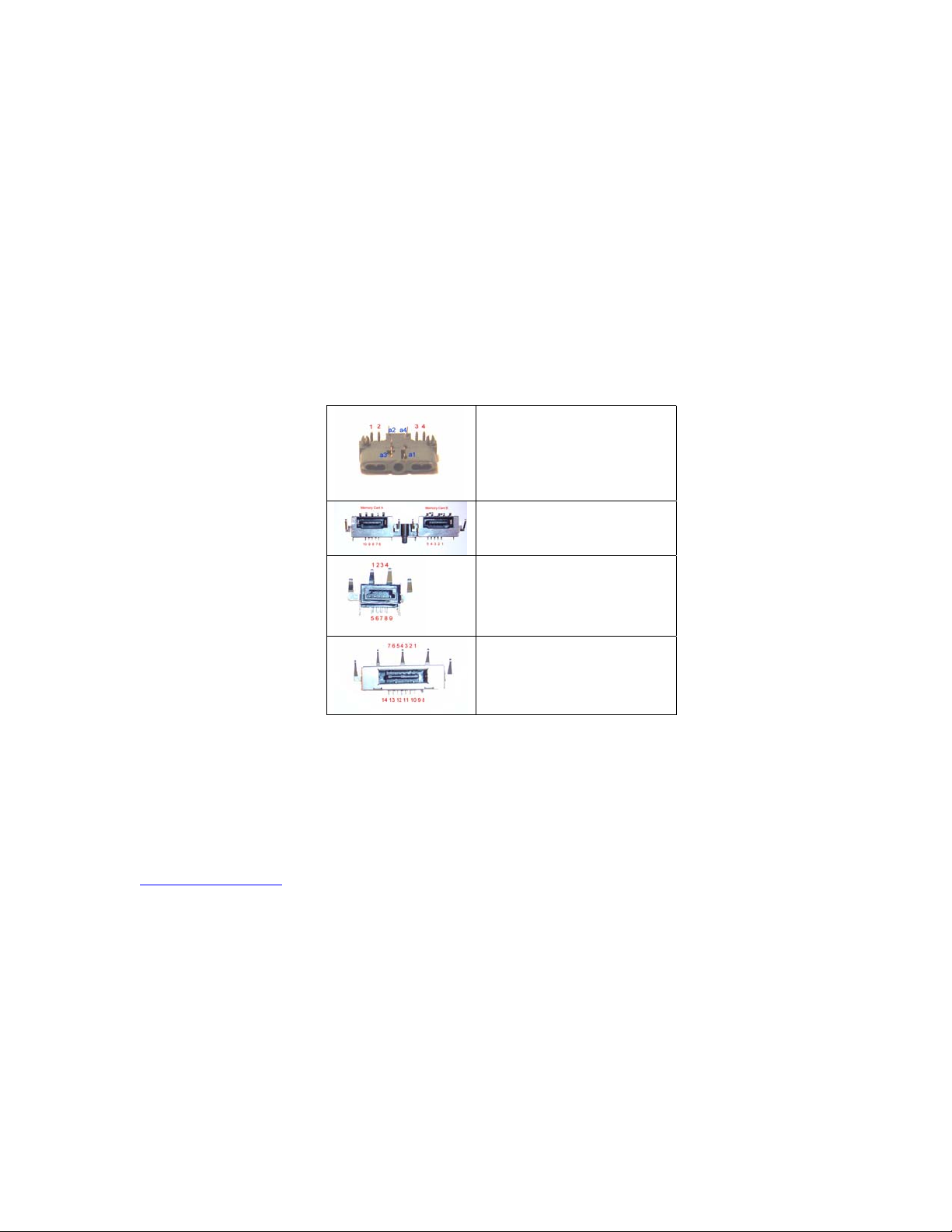
J1A1
10/100 Base-T Ethernet and USB Port
Green LED
1
Green LED
2
Yellow LED
3
Yellow LED
4
5 TD+ 13
6 CT 14
7 TD- 15
Shield GND
8
9 RD+
10 CT
11 RD-
+5 VDC
12
Data -
Data +
GND
16 Pin 9 J6G1
Manufacturer: Bel Stewart Connectors
Product Name and #: Magjack SI-80039-F
Notes:
Green and Yellow LEDs are not present, but all the connection are available on
the 360 Motherboard. (Version 11)
LEDs are present on the 360's XDK motherboard. (Version 9)
Pin 16 connects to Pin 9 of J6G1 the RF Module.
3
J2A1
Video and Audio Port
1 Red Gnd 2 Green Ground
3 Red (Cr in HDTV mode) 4 Green (Y in HDTV mode)
5 Composite Gnd 6 Blue Ground
7 Composite (Sync in RGB mode) 8 Blue (Cb in HDTV mode)
9 H-sync Gnd 10 V-sync Gnd
11 H-sync (VGA Mode) 12 V-sync (VGA Mode)
13 Audio-R Gnd 14 Audio-L Gnd
15 Audio-R 16 Audio-L
17 Switching voltage (for SCART pin-8) 18 CBL-ID1
19 Blanking Signal (for SCART pin-16) 20 CBL-ID1.1
21 Unknown 22 CBL-ID2
23 Unknown 24 CBL-ID2.1
25 Optical - Audio (SPDIF) 26 CBL-ID3
27 Optical - Gnd (SPDIF) 28 CBL-ID3.1
29 Optical - +5V 30 See J2B1 or J8C1
Setting Cable ID:
ID1-1.1 = VGA mode enabled
ID2-2.1 and ID3-3.1 = RGB (SCART) mode enabled
ID3-3.1 = HDTV (Y/Cb/Cr) mode enabled
ID2-2.1 = Composite (TV) mode enabled
Manufacturer: Unknown
Product: Unkown
Note:
Source:
www.free60.org
(corrected Pin#s and added pin 30)
4
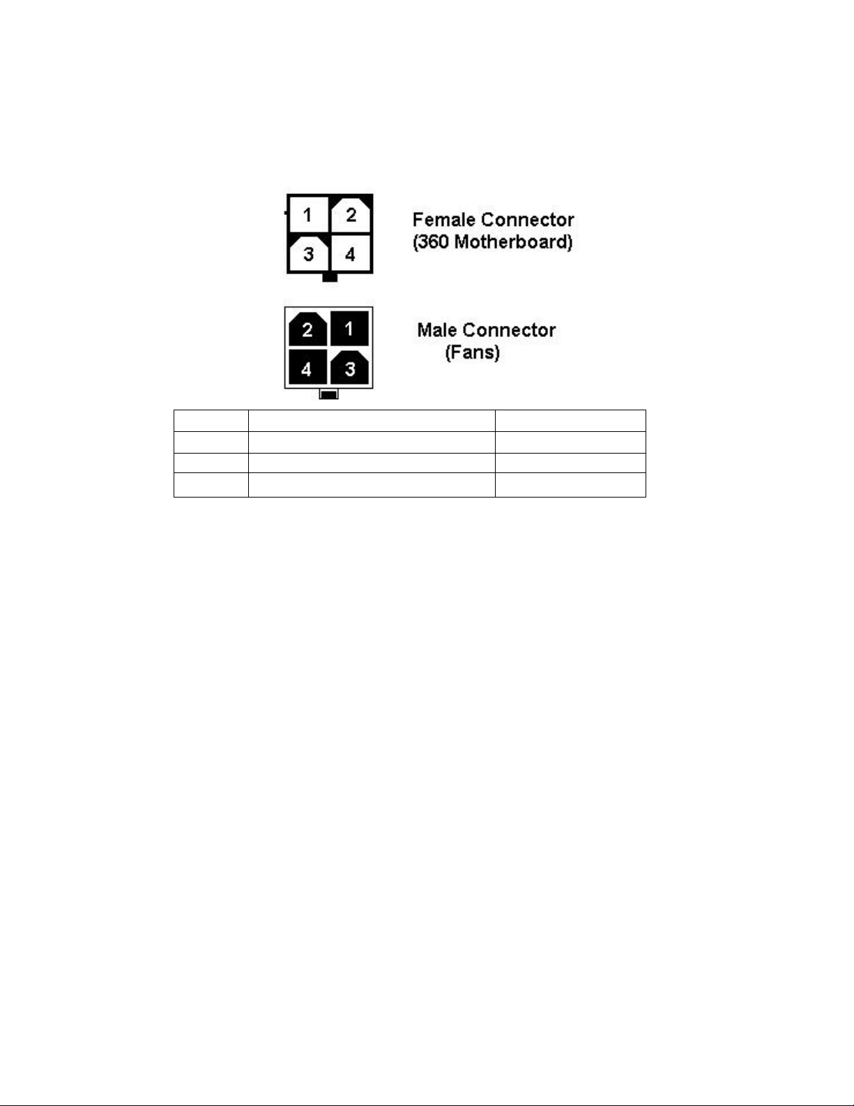
J3A1
Fan Connector
1 GND Blue
2 V+ Brown
3 GND Black
4 V+ Red
Manufacturer: Foxconn
Product:
Note:
V+ Starts at +5.4 VDC and climbs to +11.8 VDC within 30 sec of power on.
5
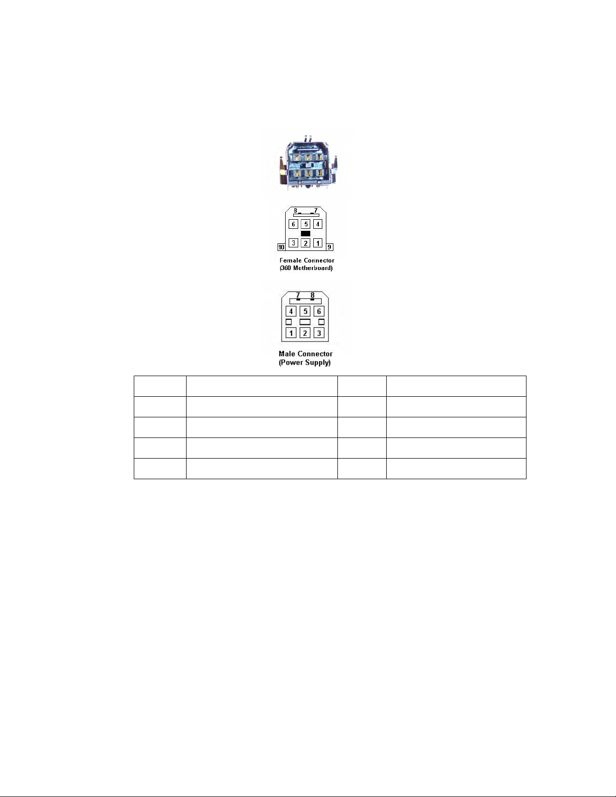
J9A1
DC Power Port
1 GND 6 +12 VDC
2 GND 7 Power Enable
3 GND 8 +5 VDC (Standby)
4 +12 VDC 9 Shield (GND)
5 +12 VDC 10 Shield (GND)
Note:
Pin 7 Turns Pins 4, 5, 6 on when it is tied to ground.
Power Supply is difficult to open up. I would not recommend it.
1) Remove rubber feet (they are glued in place). This will probably destroy them.
2) Dig out all the glue, including the glue in the head of the philips screws.
3) Remove the 4 screws.
4) Remove bottom cover.
5) Remove the two philips screws. One on each side of the heat sink.
6) Gently wiggle circuit board out of the top cover. The DC supply side should lift
up first. Heat sink grease is preventing the easy removal of the circuit board.
Continue to wiggle the circuit board until the grease bond is broken.
6
1 +5 VDC (Standby) 2 GND
Manufacturer: Unknown
Part #: Unknown
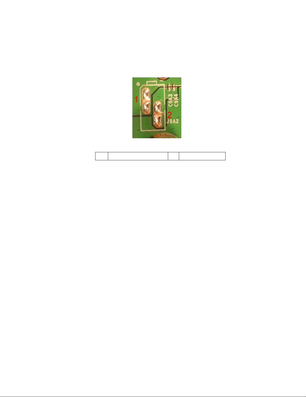
J9A2
XDK DC Power
Note:
This connector is used to supply power to the extra circuitry used in the XDK
(motherboard version 009).
The circuitry is located in the "Sidecar" that attaches to the hard drive side of the
xbox 360.
7

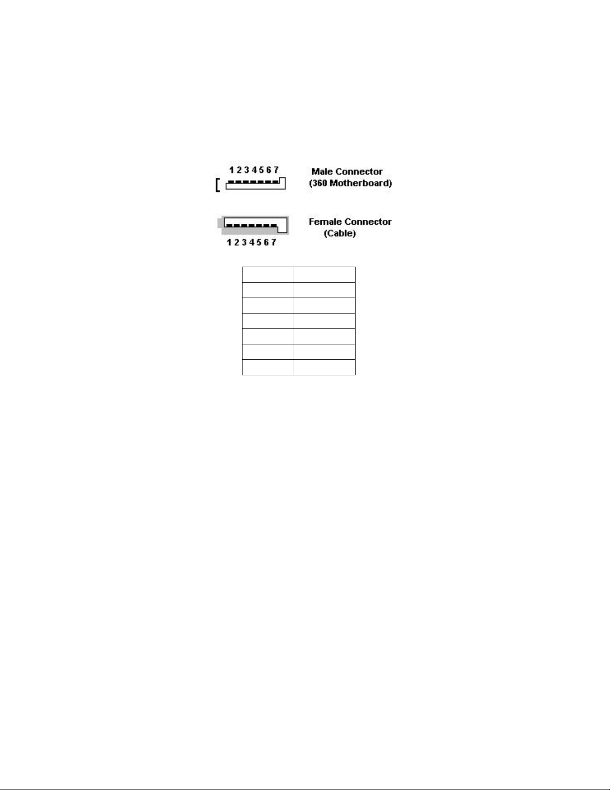
J2B1
XDK Debug Header
1
2
3 NC 0 0 No
4 Connects to U2C1 pin 16B +3.3 VDC +3.3 VDC No
5
6 Connects to U2C1 pin 16C 0 0 No
7 +3.3 VDC (Standby) +3.3 VDC +3.3 VDC No
8 +3.3 VDC +3.3 VDC 0 No
9 SDA +3.3 VDC +3.3 VDC Yes
10 SCL +3.3 VDC +3.3 VDC Yes
11 See Schematics +3.3 VDC +3.3 VDC No
12 GND 0 0 No
13 +5 VDC (Standby) +3.3 VDC +5 VDC No
Note:
1) Speculation: Document posted on xboxhacker.net and free60.org suggests that these pins are UART operating at
115000 bps.
2) Quick pulse Ejects, otherwise 360 immediately shuts down.
RX - U2C1 pin 15D
TX- U2C1 pin 14D
Eject
1
1
2
Power ON Power Off Data Present
+3.3 VDC 0 No
+3.3 VDC 0 No
+3 VDC 0 No
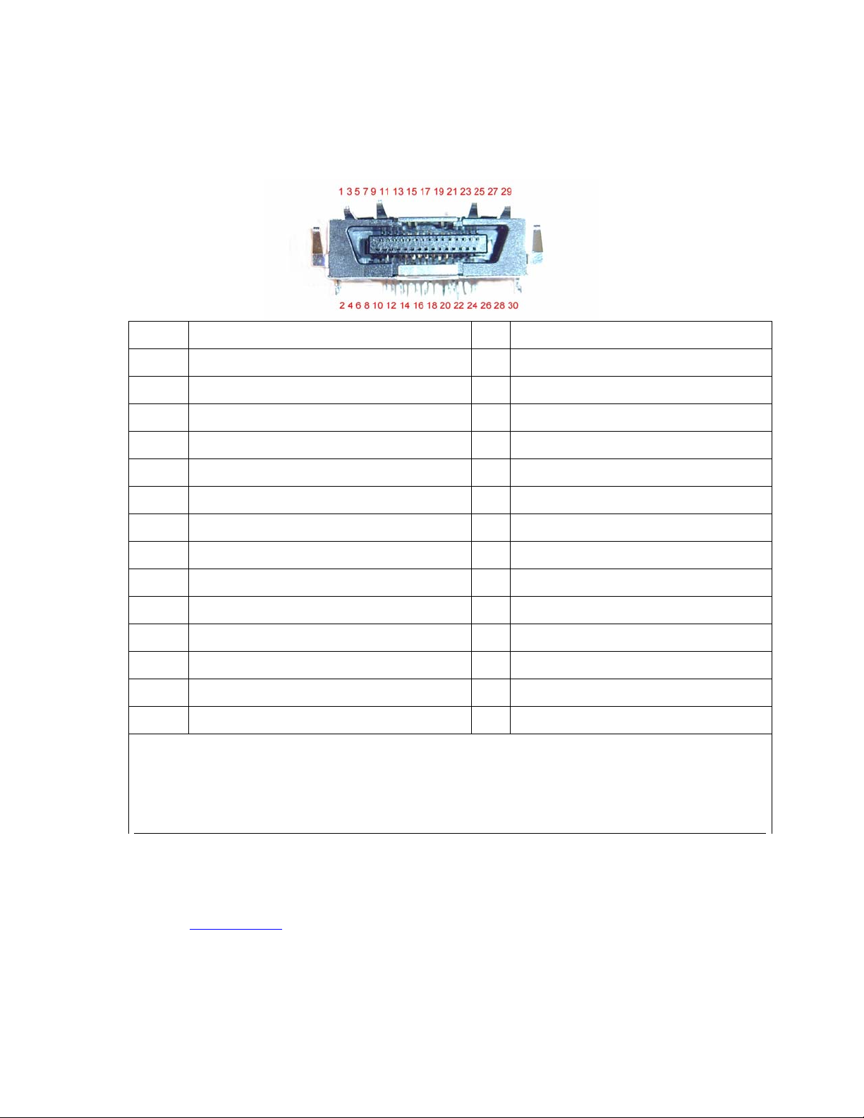
8
J1C1
DVD SATA Connector
1 GND
2 A+
3 A4 GND
5 B6 B+
7 GND
Manufacturer:
Part #:
Note:
Standard SATA interface.
Each DVD drive has a unique ID key. (source: www.xboxhacker.net)
Unkown
Tyco
9

J5C1
ANA Header
Power ON Power Off Data Present
1 Connects to Pin 71 of U4B1 +1.8 VDC +1.8 VDC No
2 Connects to Pin 70 of U4B1 +1.8 VDC +1.8 VDC No
3 Connects to Pin 69 of U4B1 0 0 No
4 Unknown 0 0 No
5 Connects to Pin 72 of U4B1 0 0 No
6 GND 0 0 No
10

J5C2
GPU SPI EEPROM Header
Power ON Power OFF Data Present
1 SCK 0 0 high on startup
2 SO 0 0
3 SI 0 0
4 /WP +1.8 VDC +1.8 VDC
5 /CS +1.8 VDC +1.8 VDC brief activity at startup
6 GND 0 0
Note:
11

J8C1
CPU JTAG Header
Power ON Power OFF Data Present
1 0 0 No
2 +1.1 VDC 0 No
3 +1.8 VDC +1.8 VDC 0 No
4 +1.8 VDC 0 No
5 GND 0 0 No
6 +1.8 VDC 0 No
7 +1.8 VDC 0 No
8 +1.8 VDC 0 No
9 +3.3 VDC +3.3 VDC No
10 +1.8 VDC 0 No
Note:
Images indicate this port was used during hardware development.
Pin 9 was not used in HDK image.
The pin header is also present on the XDK version 9 motherboard.
Speculation: GPULDBG, Inputs - TDI, TMS, TCK, Output -TDO, and RESET
12

J1D1
DVD Power Connector
1 NC 7 GND
2 NC 8 +5 VDC
3 Open/Close 9 GND
4 Tray Status 10 +12 VDC
5 GND 11 GND
6 +3.3 VDC 12 +12 VDC
Manufacturer:
Part #:
Notes:
Open/Close: momentary tied to gnd to open/close drive door.
Tray Status: +3.3 VDC tray is open. 0 v tray is closed.
Source: www.xboxhacker.net
13

J1D2
XDK Debug Header #2
Power ON Power OFF Data Present
1 Connects to U2C1 pin 5Y 0 0 No
2 Connects to U2C1 pin 5AA +3.3 VDC +3.3 VDC No
3 Connects to U2C1 pin 3U 0 0 No
4 Connects to U2C1 pin 5AB +3.3 VDC +3.3 VDC No
5 +5 VDC (Standby) +5 VDC +5 VDC No
6 GND 0 0 No
7 GND 0 0 No
8 Unknown 0 0 No
9 Unknown 0 0 No
Note:
This port is used in the XDK version 9 motherboard. The connector is routed into
the XDK "Sidecar" expansion module.
14

J2D1
Southbridge Header
Power ON Power OFF Data Present
1 Connects to U2C1 pin 21V +1.8 VDC 0 No
2 Connects to U2C1 pin 22W +1.8 VDC 0 No
3 Connects to U2C1 pin 22V 0 0 No
4 Connects to U2C1 pin 21W 0 0 No
5 Connects to U2C1 pin 20W 0 0 No
6 GND 0 0 No
15

J2D2
GPU Header
Power ON Power OFF Data Present
1 Connects to U4D1 pin 12E +1.9 VDC 0 No
2 Connects to U4D1 pin 12F +1.9 VDC 0 No
3 Connects to U4D1 pin 12D 0 0 No
4 Connects to U4D1 pin 11G 0 0 No
5 Connects to U4D1 pin 13E 0 0 No
6 GND 0 0 No
7 See Note +1.9 VDC 0 No
8 Connects to U4D1 pin 13G 0 0 No
Note:
There are images of a XDK motherboard (version 9) on the Internet that shows a
green wire connecting Pin 5 to the Southbridge(21J).
Pin 7 - still working on it.
16

J1E1
Hard Drive SATA Connector
1 GND 8 GND
2 A+ 9 GND
3 A- 10 GND
4 GND 11 +5 VDC
5 B- 12 +5 VDC
6 B+ 13 +5 VDC
7 GND 14 +5 VDC (standby)
Manufacturer:
Part #
: XB00351-002
Unknown-Made in China
17

J1F1
Southbridge LED Header
Power ON Power OFF Data Present
1 +5 VDC +5 VDC 0 No
2 GND 0 0 No
3 Connects to U2C1 pin 20D +3.3 VDC 0 No
4 Connects to U2C1 pin 21D 0 0 No
5 Connects to U2C1 pin 22D +3.3 CLK +3.3 CLK
6 Connects to U2C1 pin 21C 0 0 No
Note:
Some images of the pre version 9 360 motherboard show LEDs connected to
this Port.
OFF- 1.25 hz
ON - Activity
18

J7F1
CPU SPI EEPROM Header
1 SCK 4 /WP
2 SO 5 /CS
3 SI 6 GND
Note:
Header and eeprom is present on 360's XDK (Version 9)
Eeprom is missing on some Version 11 motherboards.
Connects to the SPI serial eeprom (AT25020) then it probably connects to the
Misc I/O bus on the CPU.
19

J3G1
Front Memory Card A & B Connector
A B
6 GND 1 GND
7 +3.3 VDC 2 +3.3 VDC
8 USB Data - 3 USB Data -
9 USB Data + 4 USB Data +
10 GND 5 GND
Note:
USB is 3.3 VDC, Same as RF Module.
20

J6G1
RF Module Connector
1 +3.3 VDC 5 See Note
2 USB Data - 6 Serial Data
3 USB Data + 7 Serial CLK
4 GND 8 GND
9 See Note
Note:
USB is 3.3 VDC, same as memory card port
Pin 5 Power ON/OFF (momentary tied to gnd to power ON/OFF)
Pin 5 goes to southbridge 21E
Pin 9 goes to Pin 16 of J1A1 (extra pin on the back USB port) but is not
connected to anything on the RF Module.
21

J7G1
Aux Power Header
1 GND 2 +12 VDC
Note:
1) This port is not active. A resistor or jumper needs to be added to the bottom
side of the motherboard were R7V7 should be.
Header missing on 360 XDK motherboard Version 9.
Header missing on 360 Retail motherboard Version 11.
1
3 GND
22

J7G2
VID Port
1 VCC 8 VID1
2 VID4 9 PWM1
3 FBRTN 10 VID0
4 VID3 11 PWM2
5 PWRGD 12 VID5
6 VID2 13 PWM3
7 EN 14 GND
Note:
Pure Speculation
The Voltage Identification (VID) port was present on early version(s) of the 360
motherboard. (pre Version 9)
I have speculated what the connections were.
To learn more download the datasheet for the ADP3188. (Analog Devices)
23

J9G1
Front Dual USB Port
Bottom Port Top Port
1 +5 VDC 5 +5 VDC
2 USB Data - 6 USB Data -
3 USB Data + 7 USB Data +
4 GND 8 GND
24

Appendix
Document Version
Version 1.0 Dec 15, 2005 Just Pinouts
Version 1.1 Dec 30, 2005 Added Photos & Diagrams
Version 1.2 Jan 6, 2006 Changed Format
Version 1.3 Feb 2, 2006 Added Schematics
Private Release
Version 1.4 Feb 15, 2006 Corrected Schematics
Added Appendix
Added Block Diagram
Current Document
25

Unique Per Console Numbers
L = Production line in the factory
NNNNNN = Xbox in the week
Y = Year (last digit)
WW = week of the year *
FF = Factory # (05 & 06 are China, 05 appears to supply Europe and 06 supplies North
America)
MM = Month
X = unknown at this time
" " = Actual Text
* Factory 05 is a week ahead of factory 06 for the 2005 year. This means any 360 made
during the last week of December 2005 should have a WW=53 in the serial #.
Serial Number = LNNNNNNYWWFF (Source: www.xbox-linux.org)
Product ID = XXXXXXXXLNNNNNNYWWFF
Motherboard = XXXXXXXXXXXXYWWX
Console ID = XXXXXXXXXXXX
Wired MAC = Unique 12 digit (hex, meaning each digit has the possibility of being a value
of 0-F)
RF Module = XXXXXXXXXXXYWW
DVD Serial # (Hitachi-LG) = YMM"HG"XXXXXX
DVD Serial # (Toshiba- Samsung) = X"RCY"XXXXXX
26

Retail Motherboard Differences
Motherboard Version 011
CPU SPI eeprom: Present or Absent
CPU: Engraved "Canada" or "Taiwan"
Tilt Switch: Surface Mount or Thru Hole Mount
Bios Label: Present or Absent
10/100 base-TX Ethernet Transceiver: "Big" or "Small"
Header Holes: Filled in with solder, partially filled or not filled.
27

Bios/Kernel Versions and Updates
Displayed in the dashboard.
D: = Dashboard
K: = Kernel
BK: = (Backup Kernel, Bios Kernel, Base Kernel, etc) - Not sure
2.0.0198.0
First image of a XDK Launcher Screen. Show version in the right hand corner.
I'm guessing it's an Alpha. (Source Image: I forget)
2.0.1232.0 Alpha 2
Image of a XDK Launcher Screen. Alpha 2 is displayed beside version #.
(Source Image: I forget)
2.0.1839.2
XeDK release Dashboard. (smartxx images)
2.0.1888.0
Sept-Oct Production Line for Retail Release
2.0.2241.0
Late Oct-Early Nov Production Line, Nov 22 available over xbox live.
* Unknown
2.0.2255.0
Jan 30 production line, Jan 30 available over xbox live
* Improved logic around deciding if saved games should be deleted and offer the option to only
delete the profile and to leave all save data.
* Users reporting blank Friends List on the Xbox 360 dash after muting a friend while playing a
game in Backwards Compatibility mode.
* Improved synching of games played to Web and in console.
* Network settings: keyboard does now allow entry of - (dash) character in the keyboard.
* Improvements to the Xbox Guide.
* Increased accuracy of "last time played."
* Network configuration improvements for Xbox Live members in the Netherlands.
* More detailed messaging for unreadable disk or region errors.
* Blocked the Kiosk Disc from being recognized when inserted into the DVD tray.
(Source: I forget, so let me know so I can provide proper credit)
28

System Requirements
Absolute Minimum
Motherboard, Power Supply (12 volt 16amp, 5 volt 1amp), Video Cable, and a
momentary pushbutton switch (for power on/off).
I have tested this with dashboard 1888 and 2241. A dashboard update could
change this.
Absolute Minimum to play games or DVDs
As above, but subtract the push button and add the DVD player and a wired
controller.
Absolute Minimum to play just DVDs
As above, but the remote can be used instead of the wire controller.
Remember that this could change with a dashboard update.
29

Retail
Note:
Flash Bios Version 2.0.1888.0
30

XeDK
Note:
Appears to be a final version of the XeDK.
Flash Bios Version 2.0.1839.2
Also known as XDK.
Used in conjunction with the SDK (Software Development Kit).
Most likely, the XeDK is also connected to a network with various PCs running
SDK.
Source: www.smartxx.com
31

Note:
HDK
No DVD connected.
Source: www.xavbox.com
32

Memory Map
Not in this Public Release
33

CPU Pinout
Not in this Public Release
34

GPU Pinout
Not in this Public Release
35

Southbridge Pinout
Not in this Public Release
36

Left Blank
37
 Loading...