

Page 1

UNO-3074
Celeron M/ Pentium M
Embedded Automation
Computer with Four
PCI-Slot Extensions
User Manual
i
Page 2

Copyright
This document is copyrighted, © 2007. All rights are reserved. The original manufacturer
described
No part
of this manual may be reproduced, copied, translated or transmitted in any form or by
the original manufacturer. Information provided in
to be accurate
no
responsibility for its use, nor for any infringements upon the rights of
third
parties that may result from such use.
reserves the right to make improvements to the products
in this manual at any time without notice.
any means without the prior written permission of
this manual is intended
and reliable. However, the original manufacturer assumes
Acknowledgements
Intel®, Pentium® and Celeron® are registered trademarks of Intel Corpora-
Microsoft® Windows and MS-DOS are registered trademarks of
tion.
Microsoft
®
Corp. All other product names or trademarks are properties of
their respective owners.
Support
For more information on this and other Advantech products, please visit
our websites
at: http://www.advantech.com
For technical support and service, please visit our support website at:
http://www.advantech.com/support/
Part No.
Printed in Taiwan August 2007
UNO-3074 User Manual ii
2003307402
3rd Edition
Page 3

Product Warranty (2 years)
Advantech warrants to you, the original purchaser, that each of its products will be free from defects in materials and workmanship for two years
from the date of purchase.
This warranty does not apply to any products which have been repaired or
altered by persons other than repair personnel authorized by Advantech,
or which have been subject to misuse, abuse, accident or improper installation. Advantech assumes no liability under the terms of this warranty as
a consequence of such events.
Because of Advantech’s high quality-control standards and rigorous testing, most of our customers never need to use our repair service. If an
Advantech product is defective, it will be repaired or replaced at no
charge during the warranty period. For out-of-warranty repairs, you will
be billed according to the cost of replacement materials, service time and
freight. Please consult your dealer for more details.
If you think you have a defective product, follow these steps:
1. Collect all the information about the problem encountered. (For
example, CPU speed, Advantech products used, other hardware
and software used, etc.) Note anything abnormal and list any
onscreen messages you get when the problem occurs.
2. Call your dealer and describe the problem. Please have your man-
ual, product, and any helpful information readily available.
3. If your product is diagnosed as defective, obtain an RMA (return
merchandize authorization) number from your dealer. This allows
us to process your return more quickly.
4. Carefully pack the defective product, a fully-completed Repair and
Replacement Order Card and a photocopy proof of purchase date
(such as your sales receipt) in a shippable container. A product
returned without proof of the purchase date is not eligible for warranty service.
5. Write the RMA number visibly on the outside of the package and
ship it prepaid to your dealer.
iii
Page 4

Declaration of Conformity
CE
This product has passed the CE test for environmental specifications
when shielded cables are used for external wiring. We recommend the use
of shielded cables. This kind of cable is available from Advantech. Please
contact your local supplier for ordering information.
FCC Class A
Note: This equipment has been tested and found to comply with the limits
for a Class A digital device, pursuant to part 15 of the FCC Rules. These
limits are designed to provide reasonable protection against harmful
interference when the equipment is operated in a commercial environment. This equipment generates, uses, and can radiate radio frequency
energy and, if not installed and used in accordance with the instruction
manual, may cause harmful interference to radio communications. Operation of this equipment in a residential area is likely to cause harmful interference in which case the user will be required to correct the interference
at his own expense.
Technical Support and Assistance
Step 1. Visit the Advantech web site at www.advantech.com/support
where you can find the latest information about the product.
Step 2. Contact your distributor, sales representative, or Advantech's cus-
tomer service center for technical support if you need additional
assistance. Please have the following information ready before
you call:
- Product name and serial number
- Description of your peripheral attachments
- Description of your software (operating system, version, application software, etc.)
- A complete description of the problem
- The exact wording of any error messages
UNO-3074 User Manual iv
Page 5

Safety Instructions
1. Read these safety instructions carefully.
2. Keep this user manual for later reference.
3. Disconnect this equipment from DC outlet before cleaning. Do not
use liquid or spray detergents for cleaning.
4. For pluggable equipment, the power outlet shall be installed near
the equipment and shall be easily accessible.
5. Keep this equipment away from humidity.
6. Put this equipment on a reliable surface during installation. Drop-
ping it or letting it fall could cause damage.
7. Make sure the voltage of the power source is correct before con-
necting the equipment to the power outlet.
8. Place the power cord such a way that people can not step on it. Do
not place anything over the power cord. The voltage and current
rating of the cord should be greater than the voltage and current rating marked on the product.
9. All cautions and warnings on the equipment should be noted.
10. If the equipment is not used for long time, disconnect it from the
power source to avoid being damaged by transient over-voltage.
11. When power core is connected, never open the equipment. For
safety reasons, the equipment should be opened only by qualified
service personnel.
12. If any of the following situations arises, get the equipment checked
by service personnel:
A. The power cord or plug is damaged.
B. Liquid has penetrated into the equipment.
C. The equipment has been exposed to moisture.
D. The equipment does not work well or you cannot get it to work
according to user manual.
E. The equipment has been dropped and damaged.
F. The equipment has obvious signs of breakage.
13. CAUTION: The computer is provided with a battery-powered
real-time clock circuit. There is a danger of explosion if battery is
incorrectly replaced. Replace only with same or equivalent type
v
Page 6
recommended by the manufacture. Discard used batteries according to the manufacturer’s instructions.
14. This device complies with Part 15 of the FCC rules. Operation is
subject to the following two conditions:
(1) this device may not cause harmful interference, and
(2) this device must accept any interference received, including
interference that may cause undesired operation.
15. CAUTION:
your chassis whenever you work with the hardware. Do not make
connections while the power is on. Sensitive electronic components
can be damaged by sudden power surges.
16. CAUTION: Always ground yourself to remove any static charge
before touching the motherboard, backplane, or add-on cards. Modern electronic devices are very sensitive to static electric charges.
As a safety precaution, use a grounding wrist strap at all times.
Place all electronic components on a static-dissipative surface or in
a static-shielded bag when they are not in the chassis.
17. CAUTION: Any unverified component could cause unexpected
damage. To ensure the correct installation, please always use the
components (ex. screws) provided with the accessory box.
Safety Precaution - Static Electricity
Follow these simple precautions to protect yourself from harm and the
products from damage.
1. To avoid electrical shock, always disconnect the power from your
PC chassis before you work on it. Don't touch any components on
the CPU card or other cards while the PC is on.
2. Disconnect power before making any configuration changes. The
sudden rush of power as you connect a jumper or install a card may
damage sensitive electronic components.
Always completely disconnect the power cord from
UNO-3074 User Manual vi
Page 7

Contents
Chapter 1 Overview .......................................................... 2
1.1 Introduction ....................................................................... 2
1.2 Hardware Specifications ................................................... 5
1.3 Safety Precautions ............................................................. 7
1.4 Chassis Dimensions........................................................... 8
1.5 Packing List..................................................................... 10
Chapter 2 Hardware Functionality ............................... 12
2.1 Introduction ..................................................................... 12
2.2 RS-232 Interface (COM1~COM2) ................................. 13
2.3 RS-232/422/485 Interface (COM3~COM4) .................. 13
2.4 LAN: Ethernet Connector ............................................... 17
2.5 Onboard Isolated Digital Input........................................ 17
2.6 Onboard Isolated Digital Output ..................................... 21
Figure 1.1:Chassis Dimensions for CeleronM 1GHz .... 8
Figure 1.2:Chassis for Pentium 1.8GHz or Faster CPU 9
Figure 1.3: Accessories ................................................ 10
Figure 2.1:Front Panel of UNO-3074 .......................... 12
2.3.1 16C550 UARTs with 16-byte FIFO Standard ............. 13
2.3.2 RS-422/485 Detection .................................................. 13
2.3.3 Automatic Data Flow Control Function for RS-485 ... 13
2.3.4 RS-232/422/485 Selection ........................................... 14
Figure 2.2:RS-422/485 Jumper Setting ....................... 14
Figure 2.3:RS-232 Jumper Setting ............................... 14
2.3.5 RS-485 Auto Flow/RS-422 Master/Slave Selection .... 14
Table 2.1:Auto Flow & RS-422 Slave/Masters ........... 15
2.3.6 IRQ, I/O Address and Transmission Rate Setting ....... 15
Table 2.2:IRQ Setting via Switch 1 at SW3 ................ 16
Table 2.3:Transmission Rate (Switch 2 at SW3) ......... 16
2.3.7 Termination Resistor (JP6) .......................................... 17
2.5.1 Pin Assignments .......................................................... 17
Figure 2.4:Digital Input Connector Pin Assignments .. 17
Table 2.4:Digital Input Connector Signal Description 18
2.5.2 Isolated Inputs .............................................................. 18
Figure 2.5:Isolated Digital Input Connection .............. 18
2.5.3 Interrupt Function of the DI Signals ............................ 19
2.5.4 IRQ Level .................................................................... 19
2.5.5 Interrupt Control Register ............................................ 19
Table 2.5:Interrupt Control Register Bit Map ............. 19
2.5.6 Interrupt Enable Control Function ............................... 20
Table 2.6:Interrupt Disable/Enable Control ................. 20
2.5.7 Interrupt Triggering Edge Control ............................... 20
Table 2.7:Interrupt Triggering Edge Control ............... 20
2.5.8 Interrupt Flag Bit ......................................................... 20
Table 2.8:Interrupt Flag Bit Values ............................. 20
vii Table of Contents
Page 8

2.6.1 Pin Assignments .......................................................... 21
Figure 2.6:Digital Output Connector Pin Assignments 21
Table 2.9:Digital Output Connector Signals ................ 21
2.6.2 Power On Configuration .............................................. 22
Table 2.10:Digital Output Power On Configuration ... 22
2.6.3 Isolated Outputs ........................................................... 22
Figure 2.7:Isolated Digital Output Connection ............ 23
2.7 Onboard Isolated Counter/Timer .................................... 24
2.7.1 Counter/Timer Control Register .................................. 24
Table 2.11:Counter/Timer Control Register Bit Map .. 24
2.7.2 Counter 0 Function Block ............................................ 25
Figure 2.8:Counter 0 Function Block .......................... 25
2.7.3 Counter 1 Function Block ............................................ 25
Figure 2.9:Counter 1 Function Block .......................... 25
2.7.4 32-bit Counter Function Block (CTR32Set=1) .......... 26
Figure 2.10:32-bit Counter Function Block ................. 26
2.7.5 Counter Clock Source .................................................. 26
Table 2.12:Counter Clock Source Control Bit ............. 26
2.7.6 Counter Internal Clock ................................................. 26
Table 2.13:Counter Internal Clock Control Bit ........... 26
2.7.7 Counter Gate Source .................................................... 26
Table 2.14:Counter Gate Source Control Bit ............... 27
2.7.8 Counter Output Destination ......................................... 27
Table 2.15:Counter Output Destination Control Bit .... 27
2.7.9 Counter Interrupt Flag ................................................. 27
Table 2.16:Counter Interrupt Flag Control Bit ............ 27
2.7.10 Cascaded 32-bit Counter .............................................. 28
Table 2.17:32-bit Counter Control Bit ......................... 28
2.8 Power Input ..................................................................... 28
Figure 2.11:Location of Power P1 and P2 ................... 28
Figure 2.12:LED Locations to Monitor Power Input .. 29
Table 2.18:Power Register Bit Map ............................ 30
2.9 LED and Buzzer for System Diagnosis........................... 30
Figure 2.13:LED Location for System Diagnosis ....... 30
Table 2.19:LED & Buzzer Control Register ............... 31
Table 2.20:Programmable LED Control Bit ................ 31
Table 2.21:Programmable Buzzer Control Bit ............ 32
2.10 USB Connector .............................................................. 32
2.11 PCMCIA: PC Card Slot .................................................. 32
2.12 VGA Display Connector ................................................. 35
2.13 Battery Backup SRAM ................................................... 37
Figure 2.14:LED Location for Battery Backup ........... 37
2.13.1 Lithium Battery Specification ...................................... 38
Figure 2.15:Lithium Battery for SRAM ...................... 38
2.14 Reset Button .................................................................... 38
Chapter 3 Initial Setup.................................................... 40
3.1 Inserting a CompactFlash Card ....................................... 40
3.2 Connecting Power ........................................................... 40
UNO-3074 User Manual viii
Page 9

3.3 Installing a Hard Disk ..................................................... 41
Figure 3.1:IDE Connector (CN1 and CN2) ................. 45
3.4 Installing a PCI-bus Card ................................................ 46
Figure 3.2:1st Anti-Vibration Rubber .......................... 46
Figure 3.3:2nd PCI-bus Card Installation .................... 47
Figure 3.4:Adjust the Anti-Vibration Rubber .............. 47
3.5 Mounting UNO-3074 ...................................................... 48
3.6 Installing Power Cable .................................................... 48
Figure 3.5: Internal Backup Power Source .................. 48
3.7 UNO-3074 Mounting Caution ........................................ 49
Figure 3.6:UNO-3074 Improper Installation (1) ......... 49
Figure 3.7:UNO-3074 Improper Installation (2) ......... 49
Figure 3.8:UNO-3074 Correct Installation .................. 50
3.8 BIOS Setup and System Assignments ............................ 51
Appendix A System Settings and Pin Assignments ......... 54
A.1 System I/O Address and Interrupt Assignments ............. 54
A.2 Board Connectors and Jumpers....................................... 56
A.3 UNO-3074 Control Register ........................................... 62
A.4 RS-232 Standard Serial Port (COM1~COM2) ............... 63
A.5 RS-232/422/485 Serial Port (COM3~COM4) ............... 64
A.6 Ethernet RJ-45 Connector (LAN1~LAN2)..................... 64
A.7 Power Screw Terminal (PWR)........................................ 65
A.8 PS/2 Keyboard and Mouse Connector ............................ 66
A.9 USB Connector (USB1~USB4) ...................................... 66
A.10 VGA Display Connector ................................................. 67
Table A.1:UNO-3074 System I/O Port ........................ 54
Table A.2:UNO-3074 Interrupt Assignments .............. 55
Figure A.1:Backplane Connector & Jumpers .............. 56
Figure A.2:Mainboard Connector & Jumpers (Back) .56
Figure A.3:Mainboard Connector & Jumpers (Front) . 57
Figure A.4:Daughter Connector & Jumpers (Front) .... 58
Figure A.5:Daughter Connector & Jumpers (Back) .... 59
Table A.3:Connector and Jumper Descriptions ........... 60
Table A.4:Connector and Jumper Descriptions ........... 60
Table A.5:Connector & Jumper Descriptions .............. 61
Table A.6:UNO-3074 Control Register ....................... 62
Table A.7:RS-232 Serial Port Pin Assigns .................. 63
Table A.8:RS-232/422/485 Serial Port Pin Assigns .... 64
Table A.9:Ethernet RJ-45 Connector Pin Assigns ....... 64
Table A.10:Power Connector Pin Assignments .......... 65
Table A.11:Keyboard & Mouse Connector Pins ......... 66
Table A.12:USB Connector Pin Assignments ............. 66
Table A.13:VGA Adaptor Cable Pin Assignmen ........ 67
Appendix B Programming the Watchdog Timer ............ 70
ix Table of Contents
Page 10

UNO-3074 User Manual x
Page 11

Overview
CHAPTER
1
This chapter provides an overview of
UNO-3074 specifications.
Sections include:
•
Introduction
•
Hardware specification
•
Safety precautions
•
Chassis dimensions
Page 12

Chapter 1
Overview
1.1 Introduction
Standard PCs and some industrial computers with a standard OS and hardware for the consumer market cannot provide the reliability required by
industrial automation and embedded
ever,
many engineers prefer to use PCs because of their advanced functions such as: analog
based
applications, and communication with third-party devices. UNO3074 combines the best features of
and powerful software, with
nature
of a PLC. UNO-3074 has the compact size and ruggedness of a PLC,
and the
software flexibility and functionality of a PC. It's an ideal platform
for sophisticated
Open Architecture Designed for Automation
For applications demanding customized control, UNO-3074 that uses
more
flexible, off-the-shelf technology is a better option. UNO-3074 uses
off-the-shelf components
CompactFlash and DRAM. System
inputs from sensors via plug-in data acquisition cards and provide outputs
to other devices to
unit
can broadcast the process data through the Ethernet and share the data
with operators
builders
require multiple inputs, optimized control, or Ethernet communication. So,
UNO-3074 offers the I/O connectivity of
100Base-T
pactFlash,
play panels.
can customize the control scheme they use for other machines that
Ethernet, 2 x RS-232, 2 x RS-232/422/485, 4 x USB, Com-
PC Card and PCI extension slots and VGA interfaces for dis-
control and simulation, database connectivity, web-
the reliability, ruggedness, and distributed
control and logging in rugged environments.
such as an x86 processor, an Ethernet chip set,
control the operation. At the same time, the UNO-3074
and managers. By using off-the-shelf components, machine
industrial control applications. How-
a PC, including the processor, RAM,
designers can easily create multiple
PCs with options such as 2 x 10/
UNO-3074 User Manual 2
Page 13

An Industry-Proven Design
Industrial and mobile applications require controllers with high-vibration
specifications and
light industrial environments also require flexible and
Many machine builders underestimate
ler
because their end applications are mounted in an industrial enclosure.
Advantech UNO-3074 has a special design without the weaknesses of a
a wide temperature range. Machines or controllers in
stable mounting.
the need for a more rugged control-
standard PC. No fan and no HDD design prevent dust and vibration problems.
A
battery-backup function secures the last state of the system, mak-
ing
system crashes less problematic. With a smart mechanical design,
UNO-3074 can
perature and almost everything
meet 50G shock, 2G vibration, up to 50° operating tem-
a harsh industrial environment demands.
Off-the-shelf Universal PCI Extensions
From a computing point of view, the UNO-3074 with its PC-based control
CPU is a high-end machine controller. It can be simply operated with the
onboard
are also available.
for plug-in data acquisition and control
GPIB cards,
providing a
Ethernet interface or with a PC Fieldbus card. Two free PCI slots
In addition, Advantech offers a complete product line
I/O cards, motion control cards,
industrial communication and Fieldbus communication cards,
complete PC-based solution.
Front Access Connections
All PC connections are on one side of the housing. The PC can optionally
be
equipped with mounting plates and fastened with screws in a control
cabinet.
plug-in
mance
All mechanical parts have a simple design, and the drivers and
cards are easily accessible without compromising system perfor-
or integrity. The installation options are also well balanced.
Designed to Fit Into Control Cabinets
The fully-fledged UNO-3074 could easily be mistaken for a PLC by its
look and feel. In
sures
180 x 177 x 237 mm (W x H x D). But the UNO-3074 not only deals
with PLC tasks, but also offers all
of a modern PC with its Intel Celeron or
dows Operating System software. So, Adventech UNO-3074 is a
powerful and inexpensive
completely new packaging, the smallest UNO only mea-
the operating and communication power
Pentium III processor and Win-
small,
PLC substitute.
3 Chapter 1
Page 14

Onboard DI/O for Counter, Alarm/Event Handling
UNO-3074 features onboard DI and DO. These DIs and DOs can be used
as
32-bit counters or to handle alarms and events. Any events can be
passed to UNO-3074
UNO-3074 can
notify key
personnel about urgent events.
through DIs with an additional DI plug-in card.
also output alarms through onboard DOs immediately to
Flexible Networking Options
UNO-3074 offers three ways to connect to a network: Ethernet, Wireless
LAN
and Modem. The two built-in Ethernet ports provide high-speed net-
working capability up to 100 Mbps.
The PCMCIA extension with PCMCIA wireless LAN module offers you a mobile and scalable network
without incurring additional cabling costs. And
UNO-3074,
working method by
industrial modems offer the most popular and easiest net-
PSTN.
through COM ports of
Popular Operating Systems and Rapid Application Development
UNO-3074 supports the popular off-the-shelf Microsoft Windows 2000/
NT/XP
operating systems and the Linux operating system. UNO-3074 also
features
tions
ers.
pre-built Microsoft Windows XP embedded or Windows CE solu-
offering a pre-configured image with optimized onboard device driv-
Microsoft Windows CE and XP Embedded are compact, highly
efficient, and real-time operating systems that are designed for embedded
systems
developing onboard device
custom
without a HDD. There is no need to waste time and energy on
drivers or using the Platform Builder to build a
Windows CE image, they have all been done for the Advantech
UNO-3000 series. Through the built-in runtime library and Software
Development Kit
Windows-based
(SDK), the UNO-3000 series leverages your existing
programming skills to rapidly develop applications.
UNO-3074 User Manual 4
Page 15

1.2 Hardware Specifications
•
CPU:
•
System Memory:
• Battery Backup RAM: 512 KB
• Chipset:
Intel 855GME GMCH/ICH4 Chipset 400 MHz PSB
(Celeron M 1G MHz Pentium M 1.4 GHz Pentium M 1.8G Hz)
•
BIOS: Award 4 Mbit Flash BIOS, supports Boot-on-LAN function
•
Interface I/O:
•
Clock:
Battery-backup RTC for time and date
•
Serial Ports: 2 x RS-232 and 2 x RS-232/422/485 with DB-9 connector
and Automatic RS-485
•
RS-232 Speed:
•
RS-422/485 Speed:
•
LAN:
Tw o 10/100Base-T RJ-45 ports
•
USB Interface:
•
CompactFlash Slots:
•
LEDs: Power, Power input 1 & 2, Power fault, IDE and
4 COM ports Tx /Rx, Alarm for battery backup
•
Four PCI-bus Slots support:
• One PC Card-bus Slot:
VGA/Keyboard/Mouse
50 bps ~ 115.2 kbps
Four USB ports, USB UHCI, Rev. 2.0 compliant
Celeron M 1GHz CPU (non-cache) or
Pentium M 1.4GHZ CPU( 2MB cache) or
Pentium M 1.8GHz CPU( 2MB cache)
1x 200 pin SODIMM socket,
supports up to 1GB DDR RAM
(
DB-15 VGA Connector, PS/2
data flow control
50 bps ~ 921.6 kbps
One internal and one external
12 V @ 5 A
-12 V @ 0.8
5 V @ 8 A
3.3 V @ 6 A
CardBus (Card-32) Card and 16-bit
(PCMCIA 2.1/JEIDA4.2) Card
+5V, +3.3V &12V@120mA working power
keyboard & mouse)
A
Diagnosis
5 Chapter 1
Page 16

• 4-ch Isolated Digital Input (DI0~DI3)
- 2,000 VDC isolation
- 2,000 VDC
- 70 VDC
- -50~50 VDC input range and 10 kHz
ESD protection
over-voltage protection
speed
- Input Voltage Range:
Logic 0: -3 ~ 3 VDC
Logic 1: -50 ~ -10 VDC, 10 ~ 50 VDC
- Input Current:
10 VDC: 1.7 mA (typical)
12 VDC:
24 VDC:
48 VDC:
50 VDC:
-
Interrupt handling capability
•
4-ch Isolated Digital Output (DO0~DO3)
2.1 mA (typical)
4.4 mA (typical)
9.0 mA (typical)
9.4 mA (typical)
- 2,000 VDC isolation and 200 mA max / channel sink current
- 2 options after hot reset: Reset all digital output or keep last status
- 5 ~ 40 VDC output range and 10 kHz speed
•
Two 16-bit Counters/Timers:
- Counter source: DI1 & DI3, Pulse output: DO2 & DO3
- Can be cascaded
- Down
- Interrupt
counting, preset counting value
- Internal timer time
•
HDD: HDD extension kit for installation of one standard 2.5” (optional)
•
Anti-Shock:
as one 32-bit counter/timer
handling, speed: 40 kHz
base: 100 kHz, 10 kHz, 1 kHz, 100 Hz
20 G @ Wall mounting, IEC 68 section 2-27, half sine, 11 ms w/HDD
50 G @ Wall mounting, IEC 68 section 2-27,
•
Anti-Vibration:
half sine, 11 ms w/CF
2 Grms w/CF@IEC 68 sec. 2-64, random, 5~500Hz, 1 Oct./min,1hr axis
UNO-3074 User Manual 6
Page 17

1 Grms w/HDD@IEC 68 sec. 2-64, random, 5~500Hz, 1 Oct./min, 1hr axis
•
Power Supply:
•
Operating Temperature:
• Relative Humidity:
•
Power Consumption: 24 W (Typical)
•
Power Requirement: Min 96 W, (16~36 VDC) (e.g. +24 V @ 4A)
•
Chassis Size (WxHxD):
180 x 237 x 179 mm (7.1" x 9.3" x 7.0") for Celeron-M 1GHz CPU
193 x 237 x 179 mm (7.6" x 9.3" x 7.0") Pentium-M 1.8GHz or faster CPU
• Mounting:
• We i g h t :
•
Software OS:
16 ~ 36 VDC
-10 ~ 55° C (14 ~ 131° F)
0~95% @ 40° C (non-condensing)
Wall/Panel/Stand mounting
5.0 kg for Celeron-M 1GHz CPU
6.0 kg for Pentium-M 1.8GHz or faster CPU
Windows XP Embedded/CE 5.0/2000/XP, Linux
1.3 Safety Precautions
The following messages inform how to make each connection. In most
cases,
you will simply need to connect a standard cable.
Note:
Always disconnect the power cord from your chassis whenever you are working on it.
while the power is on. A sudden rush of power can
damage sensitive electronic components. Only
experienced electronics personnel should open the
chassis.
Do not connect
Note: Always ground yourself to
Note:
tric charge
electronic
tric charges. Use
times.
dissipative
If DC voltage is supplied by an external circuit,
please put a protection
input
before touching UNO-3074. Modern
devices are very sensitive to static elec-
a
grounding wrist strap at all
Place all electronic components on a static-
surface or in a static-shielded bag.
device in the power supply
port.
7 Chapter 1
remove any static elec-
Page 18
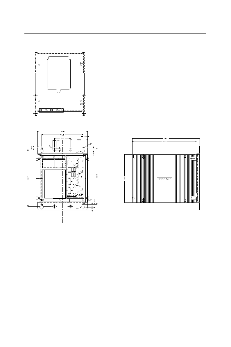
1.4 Chassis Dimensions
Figure 1.1: Chassis Dimensions for CeleronM 1GHz
UNO-3074 User Manual 8
Page 19

Figure 1.2: Chassis for Pentium 1.8GHz or Faster CPU
9 Chapter 1
Page 20

1.5 Packing List
The accessory package of UNO-3074 contains the following items:
(A) Power cable
(B) Keyboard/ Mouse PS/2 cable
(C) Warranty card
(D) Driver and Utility CD-ROM
(E) 4 x nti-vibration rubber
(F) PCI expansion to hold 2nd anti-vibration rubber
(G) Mini Jumper
(H) Paper menu
( I ) Power connector
(J) IDE cable for 2.5" HDD
Figure 1.3:
UNO-3074 User Manual 10
Accessories
Page 21

2
CHAPTER
Hardware Functionality
This chapter shows how to setup the
UNO-3074 hardware functions, including connecting
switches and indicators.
Sections include:
• Introduction
• RS-232 Interface
• RS-232/422/485 Interface
• LAN / Ethernet Connector
• DI/O and Counter
• Power Connector
•
LED and Buzzer
• PS/2 Mouse and Keyboard
• USB Connector
• PCMCIA: PC Card Slot
• VGA Display Connector
• Battery Backup SRAM
• Reset Button
peripherals, and setting
Connector
Page 22
Chapter 2
Hardware Functionality
2.1 Introduction
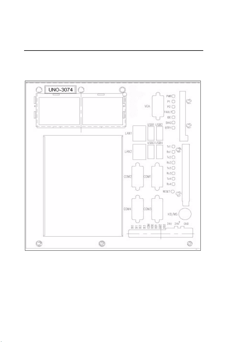
The two figures below show the connectors on UNO-3074, and following
sections give you detailed information about function of each peripheral.
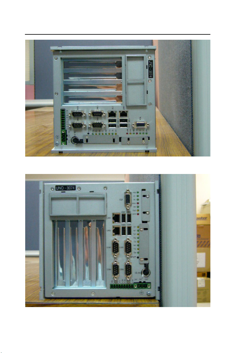
Figure 2.1:
UNO-3074 User Manual 12
Front Panel of UNO-3074
Page 23

2.2 RS-232 Interface (COM1~COM2)
The UNO-3074 offers two industrial standard RS-232 serial communication
interface ports: COM1 and COM2. Please refer to Appendix A.4 for
their pin
The IRQ and I/O address range
COM1: 3F8
assignments.
of
COM1 and COM2 are listed below:
, IRQ4 COM2: 2F8H, IRQ3
H
2.3 RS-232/422/485 Interface (COM3~COM4)
The UNO-3074 offers two industrial RS-232/422/485 serial communication interface
their pin assignments. The default setting of COM3 and COM4 are RS422/485. (Please refer to section 2.3.4 for how to determine RS-232 or
RS-422/485)
2.3.1
Advantech UNO-3074 comes with 16C550 UARTs containing 16 bytes
FIFOs.
2.3.2
In RS-422/485 mode, UNO-3074 automatically detects signals to match
RS-422 or
ports: COM3 and COM4. Please refer to Appendix A.5 for
16C550 UARTs with 16-byte FIFO Standard
RS-422/485 Detection
RS-485 networks. (Refer to section 2.3.5)
2.3.3
Automatic Data Flow Control Function for RS-485
In RS-485 mode, UNO-3074 automatically detects the direction of incoming data
shaking signal
RS-485 network
cation
can be maintained without
and switches its transmission direction accordingly. So no hand-
(e.g. RTS signal) is necessary. This lets you easily build an
with Data+, Data- and Ground. More importantly, appli-
software previously written for full-duplex RS-232 environments
modification.
13 Chapter 2
Page 24
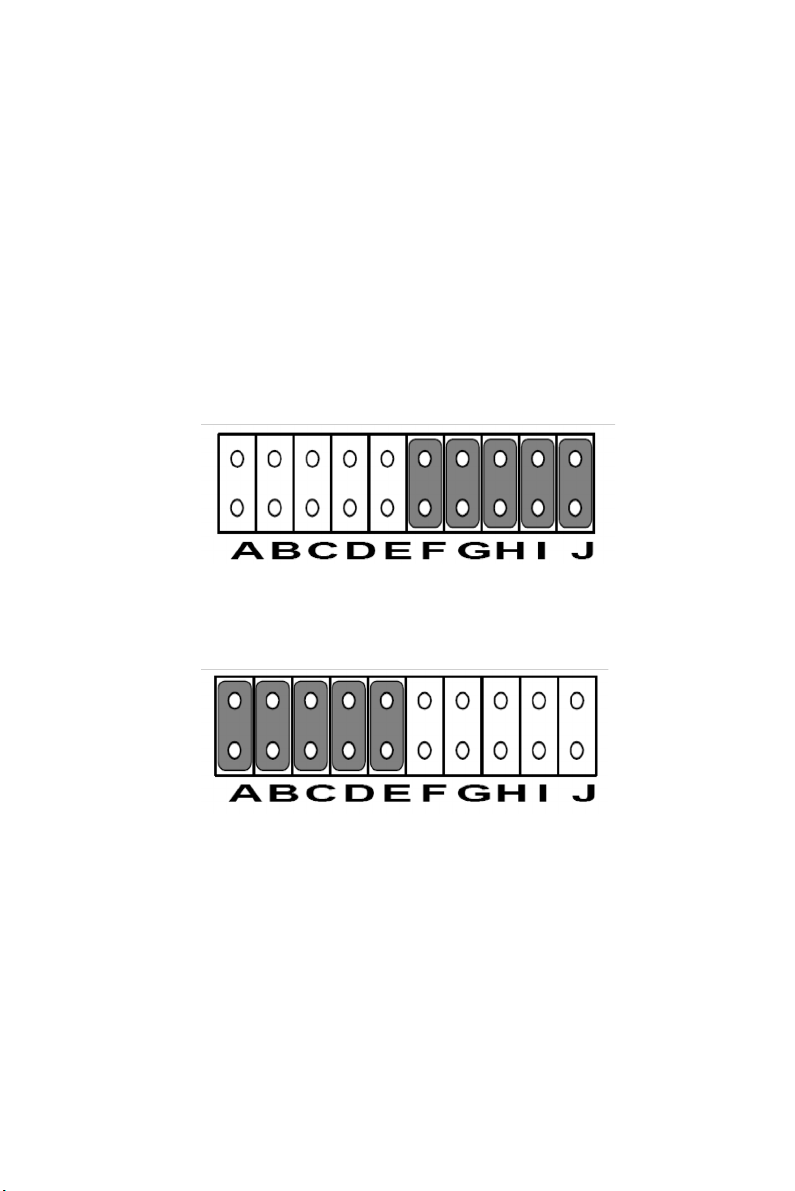
2.3.4
RS-232/422/485 Selection
COM3 and COM4 support 9-wire RS-232, RS-422 and RS-485 interfaces.
The system detects RS-422 or RS-485 signals automatically in RS-422/
485 mode.
To select
select
You can refer to figures below to set the JP4 and JP5.
between RS-422/485 and RS-232 for COM3, adjust JP4. To
between RS-422/485 and RS-232 for COM4, adjust JP5.
Note:
Jumper setting for RS-422/485 interface: (Default setting).
Jumper setting for RS-232 interface:
2.3.5
You can set the “Auto Flow Control” mode of RS-485 or “Master/Slave”
mode of RS-422
(Refer to Figure A.3 for location of SW2).
In RS-485,
the direction of the data
Then no handshaking
the driver
Please refer to Appendix A.2 Figure A.3 for location
of JP4 and JP5 location
Figure 2.2:
Figure 2.3:
RS-422/485 Jumper Setting
RS-232 Jumper Setting
RS-485 Auto Flow/RS-422 Master/Slave Selection
by
using the SW2 DIP switch for each RS-422/485 port.
if the switch is set to “Auto”, the driver automatically senses
flow and switches the direction of transmission.
is necessary. In RS-422, if DIP switch is set to “On”,
is always enabled, and always in high or low status.
UNO-3074 User Manual 14
Page 25

Table 2.1: Auto Flow & RS-422 Slave/Masters
SW2 DIP Switch Setting COM Port Mode Selections
COM3 RS-422: Slave mode
RS-485: Auto flow control
COM4 RS-422: Slave mode
RS-485: Auto flow control
COM3 RS-422: Master mode
RS-485: N/A
COM4 RS-422: Slave mode
RS-485: Auto flow control
COM3 RS-422: Slave mode
RS-485: Auto flow control
COM4 RS-422: Master mode
RS-485: N/A
COM3 RS-422: Master mode
RS-485: N/A
COM4 RS-422: Master mode
RS-485: N/A
2.3.6
IRQ, I/O Address and Transmission Rate Setting
The IRQ and I/O address range of COM3 and COM4 are listed below:
•
COM3:
•
COM4: 2E8H, IRQ5 (Independent IRQ), IRQ10 (Share IRQ)
•
Vector address for share IRQ:
3E8H, IRQ10 (Independent IRQ), IRQ10 (Share IRQ)
1D0
H
Yo u can set “Share IRQ” or “Independent IRQ” by the first switch of SW3
(Refer to Table 2.2 below).
15 Chapter 2
Page 26

Table 2.2: IRQ Setting via Switch 1 at SW3
Switch 1 at SW3 setting Function
1
2
1
2
O
N
O
N
Share IRQ (default)
Independent IRQ
Note: Please Refer to Figure A.3 for location of SW3
Note: After changing the jumper, please also adjust the IRQ
through the device manager software for the new settings to work properly. (Refer to UNO Serial Port Installation Guide in the CD, steps 7 ~ 10)
Table 2.3: Transmission Rate (Switch 2 at SW3)
Switch 2 at SW3 setting Function
1
2
O
N
Speed x 8*
1
2
O
N
Speed x 1 (default)
Yo u can adjust the transmission rate by the second switch of SW3.
* To increase
the normal baud rates by eight times, (e.g. if we set the baud
rate as 115.2K bps in software, then the actual hardware baud rate will be
increased
to 921.6K bps), set switch 2 of SW3 to “on”.
Note: Only COM3 and COM4 can adjust the transmission rate.
UNO-3074 User Manual 16
Page 27

2.3.7 Termination Resistor (JP6)
The onboard termination resistor (120 ohm) for COM3/COM4 can be
used for long distance
COM3 Close A TX3-TR Data+, Data-
COM4 Close C TX4-TR Data+, Data-
Close: Enable termination resistor.
transmission or device matching (Default Open).
RS-422 RS-485
Close B RX3-TR
Close D TX4-TR
Note:
Please refer to Figure A.3 for location of JP6
2.4 LAN: Ethernet Connector
The UNO-3074 is equipped with a Realtek RTL8139C Ethernet LAN controller
that is fully compliant with IEEE 802.3u 10/100Base-T CSMA/CD
standards.
LED indicators on the front side to show its Link (Green LED) and Active
(Yellow LED) status.
The Ethernet port provides a standard RJ-45 jack on board, and
2.5 Onboard Isolated Digital Input
The UNO-3074 has 4 isolated DI channels designated DI0~DI3.
2.5.1
Pin Assignments
The connector type of UNO-3074 is plug-in screw terminal block that
enables
you to connect to field I/O devices directly without additional
accessories. Figure 2.4 and Table 2.4 shows its pin assignment as well as
signal description.
Figure 2.4:
Digital Input Connector Pin Assignments
17 Chapter 2
Page 28

Table 2.4: Digital Input Connector Signal Description
Signal Name Reference Direction Description
DI <0...3> COM Input Isolated DI signal s
COM - - DI, DO isolated
ground
2.5.2
Isolated Inputs
Each of isolated digital input channels accepts 0 ~ 50 VDC voltage inputs,
and
accepts bi-directional input. The voltage range is -3 ~ 3 VDC for logic
0 (low), -50 ~ -10 VDC and 10 ~ 50 VDC for logic 1 (high). It means that
you can apply positive or negative voltage to an isolated input pin (Vin).
All
channels share one common pin (COM). Figure 2.5 shows how to con-
nect an external
input source to one of the UNO-3074 isolated input chan-
nels.
Please note
Counter 0 and Counter 1;
pins of Counter 0
that DI0 and DI2 may be configured as gate control pins of
While DI1 and DI3 may be configured as input
and Counter 1. Please refer to section 2.7 for
details
Note: Refer to Appendix A.3 Table A.6 for command of DI
Figure 2.5:
UNO-3074 User Manual 18
Isolated Digital Input Connection
Page 29

2.5.3
Interrupt Function of the DI Signals
DI0 and DI1 can be used to generate hardware interrupts. Users can setup
the configuration of them
The channels are connected to the interrupt circuitry.
enable interrupt
ting
the Interrupt Control Register of the UNO-3074 (refer to section 2.5.5
below). When
service
these interrupt requests by ISR (Interrupt Service Routine). The
function, select trigger type or latch the port data by set-
the interrupt request signals occur, then the software will
by
programming the interrupt control register.
Users can disable/
multiple interrupt sources provide the card with more capability and flexibility.
2.5.4
IRQ Level
The IRQ level is by default set by the system BIOS. IRQ 7 is reserved for
DI
interrupt and counter interrupt.
2.5.5
Interrupt Control Register
Table 2.5: Interrupt Control Register Bit Map
Base Address 7 6 5 4 3 2 1 0
202H R/W Interrupt Enable Control/Status Register
DI1EN DI0EN
203H R/W Interrupt Triggering Edge Control/Status Register
DI1TE DI0TE
207H R/W Interrupt Flag/Clear Register
DI1F DI0F
The Interrupt Control Register controls the function and status of each
interrupt
trol Register. The register is
ten, it
signal source. Table 2.5 shows the bit map of the Interrupt Con-
readable/writeable register. While being writ-
is used as a control register; and while being read, it is used as a sta-
tus register.
DI0EN & DI1EN: DI0 & DI1
DI0TE & DI1TE: DI0 & DI1 Interrupt triggering edge control
DI0F & DI1F:
DI0 & DI1 interrupt flag bit
Interrupt disable/enable control bit
bit
19 Chapter 2
Page 30
2.5.6
Interrupt Enable Control Function
Table 2.6: Interrupt Disable/Enable Control
DI0EN & DI1EN Interrupt Disable/Enable Control
0 Disable
1 Enable
The user can choose to enable or disable the interrupt function by writing
its corresponding
interrupt control
2.5.7
Interrupt Triggering Edge Control
value to the interrupt disable/enable control bit in the
register, as shown in Table 2.6.
The interrupt can be triggered by a rising edge or a falling edge of the
interrupt signal, as
control
bit in the interrupt control register, as shown in Table 2.7.
determined by the value in the interrupt triggering edge
Table 2.7: Interrupt Triggering Edge Control
DI0TE & DI1TE Triggering edge of interrupt signal
0 Falling edge trigger
1 Rising edge trigger
2.5.8 Interrupt Flag Bit
The interrupt flag bit is a flag indicating the status of an interrupt. It is a
readable/writable bit. To find the status of the interrupt, you
the bit
value. To clear the interrupt, you have to write “1” to this bit. This
bit must first be cleared to
service the next coming interrupt.
Table 2.8: Interrupt Flag Bit Values
DI0F & DI1F Interrupt Status
Read
Write 0 Don’t care
UNO-3074 User Manual 20
0 No interrupt
1 Interrupt occur
1 Clear interrupt
have to read
Page 31

Note: UNO-3074 provides built-in examples to show how to
deliver digital input functionality. Refer to console mode
examples in
C:\Program Files\Advantech\UNO\UNO_IsaDIO\Examples\Console.
(Please install DI/O driver from the UNO CD to use
these examples)
2.6 Onboard Isolated Digital Output
The UNO-3074 has 4 isolated DO channels designated DO0 ~ DO3.
2.6.1
Pin Assignments
The connector type of UNO-3074 is plug-in screw terminal block that
enables
you to connect to field I/O devices directly without additional
accessories. Figure 2.6 and Table 2.9 show its pin assignment as well as
signal description.
Figure 2.6:
Digital Output Connector Pin Assignments
Table 2.9: Digital Output Connector Signals
Signal Name Reference Direction Description
DO <0...3> COM Output Isolated DO signals
COM - - DI, DO isolated
ground
21 Chapter 2
Page 32

2.6.2
Power On Configuration
Default configuration after power on or hardware reset is to set all the isolated digital
sink) so
system
lated digital
the configuration of
output channels to open status (the current of the load can’t be
that users need not worry about damaging external devices during
startup or reset. When the system is hot reset, then the status of iso-
output channels are selected by jumper JP7. Table 2.10 shows
jumper JP7.
Note: Please refer to Figure A.3 for location of JP7
Table 2.10: Digital Output Power On Configuration
JP7
2.6.3
Isolated Outputs
Power on configuration after hot reset
Reset all digital output
(default configuration)
Keep last status after hot reset
Each of isolated output channels comes equipped with a Darlington transistor. All output
Please note
lated output
rent will flow from
take care that the
2.7 below shows how
channels share common emitters.
that if an external voltage (5 ~ 40 VDC) is applied to an iso-
channel while it is being used as an output channel, the cur-
the external voltage source to the UNO-3074. Please
current through each DO pin not exceed 200 mA. Figure
to connect an external output load to the UNO-3074
isolated outputs.
Please
note that DO2 and DO3 may be configured as output pins of
Counter 0 and Counter
1 (please refer to section 2.7 for more details)
UNO-3074 User Manual 22
Page 33

Figure 2.7:
Isolated Digital Output Connection
Note: Please refer to Appendix A.3 Table A.6 for command
of DO
Note: UNO-3074 provides built-in examples to show how to
deliver digital output functionality. Refer to console
mode examples in C:\Program Files\Advantech\UNO\UNO_IsaDIO\Examples\Console. (Please
install DI/O driver from the UNO CD to use these
examples)
23 Chapter 2
Page 34

2.7 Onboard Isolated Counter/Timer
The UNO-3074 uses one 82C54 programmable timer/counter chip that
includes
counter 2.
for
input and pulse output. They can be programmed to count from 2 up to
65535 or cascaded into one 32-bit counter.
The UNO-3074 has two isolated counter input channels designated DI1
and DI3 with two isolated output channels designated DO2 and DO3.
Therefore,
function.
2.7.1
The Counter/Timer Control Register controls the function and status of
each counter/timer signal
Counter/Timer Control Register. The register is readable/writable register.
While being written, it is used as a control register; and while being read,
it
Table 2.11: Counter/Timer Control Register Bit Map
Base
Address
207H R/W Interrupt Flag/Clear Register
208H R/W 82C54 Chip Counter0 Register
three independent 16-bit down counters: counter 0, counter 1 and
Counter 0 and counter 1 are for users, and counter 2 is specified
the system and can’t be used by user. Each counter has clock input, gate
you can set each counter of 82C54 as counter function or timer
Counter/Timer Control Register
source. Table 2.11 shows the bit map of the
is used as a status register.
7 6 5 4 3 2 1 0
CTR1F CTR0F
209H R/W 82C54 Chip Counter1 Register
20BH R/W 82C54 Chip Control Register
20CH R/W Counter0 Start Control / Output Status Register
CTR0
Out
20DH R/W Counter1 Start Control / Output Status Register
CTR1
Out
20EH R/W Counter0 Setting Register
20FH R/W Counter1 Setting Register
CTR3
S1 S0 CTR1
2Set
UNO-3074 User Manual 24
CTR0
IntSet
IntSet
CTR0
OutSet
CTR1
OutSet
CTR0
GateSet
CTR1
GateSet
CTR0
Gate
CTR1
Gate
CTR0
CLKSet
CTR1
CLKSet
Page 35

CTR0F/CTR1F:
CTR0Gate/CTR1Gate:
CTR0Out /CTR1Out:
CTR0CLKSet /CTR1CLKSet: (Counter 0/1) clock source control bit
CTR0GateSet/CTR1GateSet:
CTR0OutSet/CTR1OutSet: (Counter 0 /1) output destination control bit
CTR0IntSet/CTR1IntSet: (Counter 0/1) interrupt control bit
S0/S1:
(Counter 0/1) internal clock control bit
CTR32Set:
(Counter 0/1) interrupt flag bit
(Counter 0/1) gate control bit
(Counter 0/1) output status bit
(Counter 0/1) gate source control bit
Cascaded 32-bit counter control bit
2.7.2 Counter 0 Function Block
Figure 2.8:
2.7.3
Counter 1 Function Block
Figure 2.9:
Counter 0 Function Block
Counter 1 Function Block
25 Chapter 2
Page 36

2.7.4
32-bit Counter Function Block (CTR32Set=1)
Figure 2.10:
32-bit Counter Function Block
2.7.5 Counter Clock Source
There are two clock sources available for the user counters by setting
counter clock control bits -
CTR0CLKSet and CTR1CLKSet.
Table 2.12: Counter Clock Source Control Bit
CTR0CLKSet 0 Internal clock (default)
1 External clock from digital input 1 (DI1) channel
CTR1CLKSet 0 Internal clock (default)
1 External clock from digital input 3 (DI3) channel
2.7.6 Counter Internal Clock
There are four frequency options to choose according to applications, and
it’s set by internal
Table 2.13: Counter Internal Clock Control Bit
S1 S0 Time base
0 0 100 KHz (default)
0 1 10 KHz
1 0 1 KHz
1 1 100 Hz
2.7.7
Counter Gate Source
The gate sources you select determine what kind of gate input signal to
enable your counter/timer when receiving
sources available for the
CTR0GateSet and CTR1GateSet.
clock control bits - S0 and S1.
clock input. There are two gate
user counters by setting gate source control bits -
UNO-3074 User Manual 26
Page 37

Table 2.14: Counter Gate Source Control Bit
CTR0GateSet 0 Gate source from “CTR0Gate” control bit (Default)
1 Gate source from digital input 0 (DI0) channel
CTR1GateSet 0 Gate source from “CTR1Gate” control bit (Default)
1 Gate source from digital input 2 (DI2) channel
2.7.8
Counter Output Destination
Yo u can choose the output destination of counter 0 and counter 1 by setting
“Output
Destination control bits”- CTR0OutSet and CTR1OutSet.
Table 2.15: Counter Output Destination Control Bit
CTR0OutSet 0 Output destination to “CTR0Out” status bit (Default)
1 Output destination to “CTR0Out” status bit and digital output
2 (DO2) channel
CTR1OutSet 0 Output destination to “CTR1Out” status bit. (Default)
1 Output destination to “CTR1Out” status bit and digital output
3 (DO3) channel
2.7.9
Counter Interrupt Flag
The interrupt flag bit is a flag indicating the status of an interrupt. It is a
readable/writable bit. To find the status of the interrupt, you
the bit
value; to clear the interrupt, you have to write “1” to this bit. This bit
have to read
must first be cleared to service the next coming interrupt. Besides, you can
choose if counter 0 or counter 1 generate interrupt signal by configuring
“CTR0IntSet” and “CTR1IntSet” control
bit.
Table 2.16: Counter Interrupt Flag Control Bit
CTR0F, CTR1F Counter Interrupt Status
Read 0 No interrupt
1 Interrupt occur
Write 0 Don’t care
1 Clear interrupt
CTR0IntSet, CTR1IntSet Counter Interrupt Control
0 Disable (Default)
1 Enable
27 Chapter 2
Page 38

2.7.10
You can also cascade counter 0 and counter 1 together as one 32-bit
counter/timer, and it’s
Note: UNO-3074 provides built-in examples to show how
Cascaded 32-bit Counter
configured by control bit - CTR32Set.
Table 2.17: 32-bit Counter Control Bit
0 Disable (Default)
1 Cascade counter 0 and counter 1 into one 32-bit counter
to deliver counter functionality. Refer to console
mode examples in C:\Program Files\Advantech\UNO\UNO_IsaDIO\Examples\Console. (Please
install DI/O driver from the UNO CD to use these
examples)
2.8 Power Input
UNO-3074 comes with a Phoenix connector that carries 16~36 VDC external power input,
not cause any damage to the system
power line. (Please refer to Figure 2.11 for location of power input)
The UNO-3074 supports two
refer to Appendix
and features reversed wiring protection. Therefore, it will
by reversed wiring of ground line and
individual power inputs (P1/P2). (Please
A.7 for wiring of P1 and P2)
Figure 2.11: Location of Power P1 and P2
UNO-3074 User Manual 28
Page 39

You can see the LED indicators to monitor power input situation. (Please
refer to Figure 2.12 for location of LED). If the voltage of power input
P1> 15 VDC, the P1 LED indicator will be enable (means the first power
input is used). It is the same for P2 LED indicator (to show if the voltage
of power input P2 > 15 VDC). When any voltage of P1 and P2 < 15VDC,
the Fault LED will be enable. It means that you don’t use redundancy
power input. When you have two power inputs, the system will use the
power inputs with higher voltage.
Note: UNO-3074 provides built-in examples to show how to
monitor power input status. Refer to console mode
examples in
C:\Program Files\Advantech\UNO\UNO_IsaDIO\Examples\Console.
(Please install DI/O driver from the UNO CD to use
these examples)
Figure 2.12:
LED Locations to Monitor Power Input
29 Chapter 2
Page 40

Table 2.18: Power Register Bit Map
218H R Power Register
PWR P2 P1
PWR =0, Power fail
=1, Power
P1 (24V) =0, Power
=1, Power
P2 (24V*) =0, Power
=1, Power
normal
input 1 fail
input 1 normal
input 2 fail
input 2 normal
2.9 LED and Buzzer for System Diagnosis
In a “headless application” (an application without a monitor display), it is
always
difficult to know the system status. Another PC may be needed to
monitor a headless device's status via RS-232 or
solve this problem, UNO-3074 offers
ure 2.13) and buzzer.
They can be programmed to show a systems status by
a programmable LED indicator (Fig-
LED indicator flickering and buzzer alarm.
Ethernet. In order to
Figure 2.13:
UNO-3074 User Manual 30
LED Location for System Diagnosis
Page 41

Table 2.19: LED & Buzzer Control Register
210H R/W DIAG LED Register
LEDS1 LEDS0 LEDEn
211H R/W Buzzer Register
SPKS1 SPKS0 SPKEn
LEDEn: =0,
DIAG
=1,
DIAG LED
LED disable
enable
LEDS0 and LEDS1: LED flickering speed setting bit (refer to Table 2.20)
SPKEn: =0, Speaker disable
=1,
Speaker enable
SPKS0 & SPKS1: Buzzer alarming
setting bit (refer to Table 2.21)
Note: UNO-3074 provides built-in examples to show how to
configure DIAG LED and Buzzer. Refer to console
mode examples in C:\Program Files\Advantech\UNO\UNO_IsaDIO\Examples\Console.
(Please install DI/O driver from the UNO CD to use
these examples)
Table 2.20: Programmable LED Control Bit
LEDS1 LEDS0
Light on 0 0
Fast flicker 0 1
Normal flicker 1 0
Short flicker 1 1
31 Chapter 2
Page 42

Table 2.21: Programmable Buzzer Control Bit
SPKS1 SPKS0
Beep on 0 0
Short beep 0 1
Normal beep 1 0
Long beep 1 1
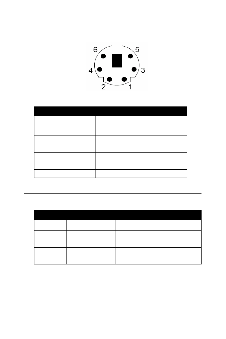
PS/2 Keyboard and Mouse Connector
The UNO-3074 provides a PS/2 keyboard and PS/2 mouse connector. A 6pin mini-DIN
connector is located on the front panel of the UNO-3074.
UNO-3074 comes with an adapter in the accessory package (see section
1.5)
to convert from the 6-pin mini-DIN connector to two 6-pin mini-DIN
connectors for PS/2 keyboard and PS/2 mouse connection. Please refer to
Appendix A.8 for its pin assignments.
2.10 USB Connector
The USB connector is used for connecting any device that conforms to the
USB interface. Many recent digital devices conform to this standard. The
USB interface supports Plug and Play,
disconnect a device whenever
The UNO-3074 provides
interface complies
face can be disabled
A.9 for its pin
with USB UHCI, Rev. 2.0 compliant. The USB inter-
in the system BIOS setup. Please refer to Appendix
assignments.
you want, without turning off the computer.
four connectors of USB interfaces. The USB
which enables you to connect or
2.11 PCMCIA: PC Card Slot
The UNO-3074 provides one PC Card slot that supports CardBus (Card-
32) cards and 16-bit (PCMCIA 2.1/JEIDA
+3.3 V, +5 V
mm
long by 54 mm wide (3.37" x 2.126"), using a 68-pin connector and a
removable module
and +12 V @ 120 mA working voltage. The PC Card is 85.6
standardized by PCMCIA that is known as “PCMCIA
card”
Note:
PCMCIA interrupt assignment is IRQ 9. If you use
Win2000 OS you need to check the IRQ manually.
UNO-3074 User Manual 32
4.2) card standards. It supports
Page 43

Note: Please don’t change the IRQ of PCMCIA adapters. This
is PCMCIA controller. (As shown by figure below) We
need to configure the IRQ of the PCMCIA device,
instead of PCMCIA controller.
For example, if you insert one PCMCIA IDE card, this card will appear in the
IDE ATA/ATAPI controllers (as the figure below). So please pay attention
that the PCMCIA will appear in the difference place of device manager
according to the type of PCMCIA. Please double click on the PCMCIA
device.
33 Chapter 2
Page 44

Make sure the IRQ of PCMCIA device is 09.
UNO-3074 User Manual 34
Page 45

2.12 VGA Display Connector
The UNO-3074 provides a VGA controller (Intel 852/855GME GMCH/
ICH4 Chipset 400 MHz PSB) for
ports CRT mode: 1280 x 1024 @ 32bpp (60Hz), 1024 x 768 @ 32bpp
(85Hz) and supports 8/16/32 MB frame buffer
Note: UNO-3074 also support 16:9 flat screen.
Note: UNO-307x VGA chipsets is similar with commercial lap-
top VGA chipsets. Sometimes if there is no image on
the monitor, it might be that VGA signal doesn’t output to
the monitor, just like when we connect a monitor to laptop VGA connector, we need to manually switch the
VGA output from laptop screen to external monitor. So
you could use hot key “CTRL+ALT+F1” to output the
VGA signal to monitor.
You can set the hot-key and other configuration for the VGA Graphics
(Please refer to the two images below)
a high resolution VGA interface. It sup-
with system memory.
35 Chapter 2
Page 46

UNO-3074 User Manual 36
Page 47

2.13 Battery Backup SRAM
UNO-3074 provides 512 KB of battery backup SRAM. This ensures that
you have a safe place to store
applications
cal
data from the memory.
There is a BTRY LED in the front
Please replace the lithium battery if
without being concerned that system crashes will erase criti-
Figure 2.14: LED Location for Battery Backup
critical data. You can now write software
panel of the UNO-3074 (Figure 2.14).
the BTRY LED is activated.
37 Chapter 2
Page 48

2.13.1
Ty p e :
Output voltage:
Location: Mainboard of UNO-3074. (Figure 2.15)
When
Lithium Battery Specification
BR2032 (Using CR2032 is NOT recommended)
3 V
DC
the voltage of battery < 2.5 VDC, BTRY LED will light up.
Figure 2.15:
Lithium Battery for SRAM
2.14 Reset Button
Press the "Reset" button to activate the reset function.
(SW1 of daughterboard)
Note:
UNO-3074 User Manual 38
Please refer to Figure A.5 for location of SW1.
Page 49

Initial Setup
This chapter introduces how to
initialize the UNO-3074.
Sections include:
•
Introduction
•
Inserting a CompactFlash Card
•
Chassis Grounding
•
Connecting Power
•
Connecting a Hard Disk
•
BIOS Setup and System Assignments
CHAPTER
3
Page 50

Chapter 3
Initial Setup
3.1 Inserting a CompactFlash Card
UNO-3074 provides two CompactFlash slots. One slot (CN4) on the
daughterboard
your
CompactFlash card directly. The other slot (CN3) is inside UNO-
3074
on
the master.
JP2 on mainboard (refer to Figures A.3)
Closed: CN3 CompactFlash on mainboard is the master
Open:
JP1 on daughterboard (refer to Figure A.4)
Closed: CN4 Compact Flash on daughterboard is master
Open: CN4 Compact Flash on daughterboard is slave
Note: Only one CompactFlash can be set as master
is accessible from the front panel, where you can insert
its motherboard. You can set JP1 and JP2 to decide which one is
CN3 CompactFlash on mainboard is slave
Internal & external CompactFlash doesn't support Hot Swap
Needs to use " Fixed Disk Mode" CompactFlash to install OS
Following is the
internal slot (CN3) of your UNO-3074. Please follow these steps carefully:
1.
Remove the power cord
2
. Unscrew the four screws from the top cover of
3.
Remove the top cover
4.
Plug a CompactFlash card with your OS and application program
into a CompactFlash card slot
5.
Screw back the top cover with four screws
procedure for the installing a CompactFlash card in the
.
UNO-3074
.
on mainboard
.
.
3.2 Connecting Power
Connect the UNO-3074 to a 16 ~ 36 VDC power source. The power
source can either be from a power adapter or an in-house
UNO-3074 User Manual 40
power source.
.
Page 51

3.3 Installing a Hard Disk
The procedure for installing a hard disk into the UNO-3074 is listed
below. Please follow these steps carefully.
1. Remove the power cord.
2. Unscrew the eight screws from the upper cover (as shown below)
3. Unscrew the HDD bracket from the upper cover.
4. Install the HDD in HDD bracket and secure with the four screws,
and then fix the HDD bracket on the upper cover.
Please refer to pictures below.
Note: When connecting IDE cable for 2.5” HDD in the
accessories bag (refer to section 1.5) to the
HDD, pay attention to the direction of IDE cable.
The correct way is shown by the first figure below
(notice the pink line).
41 Chapter 3
Page 52

UNO-3074 User Manual 42
Page 53

43 Chapter 3
Page 54

UNO-3074 User Manual 44
Page 55

5. Connect the IDE flat cable to Primary (recommended; CN1 of
mainboard) or secondary IDE connector (CN2 of mainboard), then
connect the other side of the connector to the hard disk. (Refer to
Figure 3.1 for the location of CN1 and CN2)
CN2
CN1
Figure 3.1: IDE Connector (CN1 and CN2)
Note: When you connect HDD IDE cable to the con-
nector on mainboard, please also pay attention
of the direction. The correct connection way is
shown below, notice the pink line)
6. Re-fasten the upper cover with the eight screws.
45 Chapter 3
Page 56

3.4 Installing a PCI-bus Card
The procedure for installing a PCI-bus card into the UNO-3074 is listed
below. Please
1.
2
.Remove the upper cover of UNO-3074.
3. Unscrew the screw of a PCI bracket, and remove it.
4.
5.
follow these steps carefully.
Remove the power cord.
Plug-in PCI-bus card in a PCI-slot of UNO-3074.
Screw the 1st anti-vibration rubber towards the 1st PCI card until
it is
fixed. (Figure 3.2).
Figure 3.2:
6.
Install PCI extension to hold 2nd anti-vibration rubber (Figure 3.3)
and screw the 2nd anti-vibration rubber towards the 2nd
PCI
card until it is fixed.
UNO-3074 User Manual 46
1st Anti-Vibration Rubber
Page 57

Figure 3.3:
7.
Cut off a part of the anti-vibration rubber if it is too long to fit
into the box
2nd PCI-bus Card Installation
when the PCI card is fixed.
Figure 3.4:
8.
Screw back the upper cover with the four screws.
Adjust the Anti-Vibration Rubber
47 Chapter 3
Page 58

3.5 Mounting UNO-3074
There are 3 types of mounting kits for UNO-3000 series:
• Panel mount
• Stand mount
• Wallmount
Pls refer to UNO-3000 Series Accessories Manual
Note: Due to thermal performance issues, Wallmount
will only support specific models
3.6 Installing Power Cable
UNO-3074 provides an internal backup power source so that it can provide power for a
use the power cable from accessory package (see section 1.5).
Yellow +12V
Black GND
Black GND
Red +5V
CD-ROM, DVD-ROM or other external devices. You can
Figure 3.5:
UNO-3074 User Manual 48
Internal Backup Power Source
Page 59
3.7 UNO-3074 Mounting Caution
Figure 3.6: UNO-3074 Improper Installation (1)
Figure 3.7: UNO-3074 Improper Installation (2)
49 Chapter 3
Page 60

Figure 3.8: UNO-3074 Correct Installation
Note: Because the heat transfer mechanism is designed
close to the right side of system, make sure not to
attach the right side of the UNO chassis to the wall or
ground (shown in Figure 3.10 and 3.11). It may cause
the system to hang. Instead, try to allow some space
on the right side of UNO chassis. (Figure 3.12).
Note: The UNO-3000 series is fanless and depends on the
heat sink to transfer heat. The procedure for installing
the heat-sink on the mainboard is complex, so don’t try
to move the mainboard from the chassis and backplane.
(If you uninstall the mainboard and cannot install it correctly back to chassis, the system may not be able
transfer heat and will crash)
UNO-3074 User Manual 50
Page 61

Note Please do not sperate the mainboard (illustrated
by the red circle below) from the chassis
3.8 BIOS Setup and System Assignments
UNO-3074 adapts Advantech’s SOM-4486/4481 CPU module. Further
information about the SOM-4486/4481CPU module can be found in user
manual of SOM-4486/4481.
utility CD of UNO-3074 in the accessory package.
Please note
BIOS Setup manual if
that you can try to “LOAD BIOS DEFAULTS” from the
You can find this manual on the driver and
the UNO-3074 does not work properly.
51 Chapter 3
Page 62

UNO-3074 User Manual 52
Page 63

A
APPENDIX
System Settings and
Pin Assignments
Page 64

Appendix A
System Settings and Pin
Assignments
A.1 System I/O Address and Interrupt Assignments
Table A.1:
Address Range Device
000-01F DMA controller (slave)
020-03F Interrupt controller 1 (master)
040-05F 8254 timer/counter
060-06F 8042 (keyboard controller)
070-07F Real-time clock, non-maskable interrupt (NMI)
080-09F DMA page register
0A0-0BF Interrupt controller 2 (slave)
0C0-0DF DMA controller (master)
0F0 Clear math co-processor
0F1 Reset math co-processor
0F8-0FF Math co-processor
1D0 Vector address; for COM port share IRQ
1E0 Reserved
11E Reserved
1F0-1F8 1st fixed disk
200-218 DI/O and counter
278-27F Reserved
2E8-2EF Serial port 4
2F8-2FF Serial port 2
300-31F Ethernet
360-36F LPT2
378-37F Parallel printer port 1 (LPT1)
380-38F SDLC, bisynchronous 2
3A0-3AF Bisynchronous 1
3B0-3BF Monochrome display
3C0-3CF Reserved
UNO-3074 System I/O Port
UNO-3074 User Manual 54
Page 65

Table A.1:
3D0-3DF Color/graphics monitor adapter
3F0-3F7 Diskette controller
3E8-3EF Serial port 3
3F8-3FF Serial port 1
443 Watchdog timer
DC000-DFFFF Battery backup resource
UNO-3074 System I/O Port
Table A.2: UNO-3074 Interrupt Assignments
Interrupt No. Interrupt Source
IRQ 0 Interval timer
IRQ 1 Keyboard
IRQ 2 Interrupt from controller 2 (cascade)
IRQ 3 COM2
IRQ 4 COM1
IRQ 5 COM4 (Independent IRQ)
IRQ 6 Diskette controller (FDC)
IRQ 7 DIO
IRQ 8 Real-time clock
IRQ 9 PCMCIA
IRQ 10 COM3 (Independent IRQ)/COM3&COM4 Share IRQ
IRQ 11 Reserved for watchdog timer
IRQ 12 PS/2 mouse
IRQ 13 INT from co-processor
IRQ 14 Primary IDE
IRQ 15 Secondary IDE
55 Appendix A
Page 66

A.2 Board Connectors and Jumpers
There are several connectors and jumpers on the UNO-3074 board. The
following sections tell you how to configure the UNO-3074 hardware setting. Figures A.1 to A.5 show the location of the connectors and jumpers.
Figure A.1: Backplane Connector & Jumpers
Figure A.2:
UNO-3074 User Manual 56
Mainboard Connector & Jumpers
(Back)
Page 67

Figure A.3: Mainboard Connector & Jumpers (Front)
57 Appendix A
Page 68

Figure A.4: Daughter Connector & Jumpers (Front)
UNO-3074 User Manual 58
Page 69

Figure A.5: Daughter Connector & Jumpers (Back)
59 Appendix A
Page 70

Table A.3:
Connector and Jumper Descriptions
Location Label Function
Backplane CN1 Phoenix power connector
CN2 Internal power source (Reserved)
CN3 DIO connector
CN4 Communication slot for main board
PICMG1 Communication slot for main board
PCI 1 PCI slot 1
PCI 2 PCI slot 2
PCI 3 PCI slot 3
PCI 4 PCI slot 4
Table A.4:
Mainboard CN1 Primary IDE connector
Connector and Jumper Descriptions
CN2 Secondary IDE connector
CN3 CompactFlash slot 1
CN4 Communication slot for daughterboard)
CN5 VGA DB15 display connector
P1 COM1~COM2 Standard RS-232 port
P2 COM3~COM4 RS-232/422/485 port
CON1 Ethernet1/USB1/USB2 ports
CON2 Ethernet2/USB3/USB4 ports
BH1 Lithium battery for BIOS
BH2 Lithium battery for SRAM
SW2 COM3/COM4 RS-422 master/slave selection
SW3 Share IRQ/Independent IRQ selection and
JP2 CompactFlash 1 master/slave selection
JP4 COM3 RS-232/422/485 selection
JP5 COM4 RS-232/422/485 selection
JP6 COM3/COM4 terminator resistor
JP7 Digital output latch/non-latch
Speed selection
UNO-3074 User Manual 60
Page 71

Table A.5:
Daughterboard CN1 PC card slot
Connector & Jumper Descriptions
CN2 Communication slot for mainboard
CN3 PS/2 keyboard and mouse connector
CN4 CompactFlash slot 2
SW1 Reset button
D1 COM1 Tx LED
D2 Warning LED for battery backup SDRAM
D3 COM1 Rx LED
D4 COM2 Tx LED
D5 COM2 Rx LED
D6 COM3 Tx LED
D7 COM3 Rx LED
D8 COM4 Tx LED
D9 COM4 Rx LED
D10 Diagnostic LED
D11 IDE LED
D12 PWR LED
D13 P1 (Power input 1) LED
D14 P2 (Power input 2) LED
D15 Power fault LED
JP1 CompactFlash 2 master/slave selection
61 Appendix A
Page 72

A.3 UNO-3074 Control Register
Table A.6: UNO-3074 Control Register
Base
Address
200H R Isolated Digital Input Status Register
201H R/W Isolated Digital Output Control/Status Register
202H R/W Interrupt Enable Control/Status Register
203H R/W Interrupt Triggering Edge Control/Status Register
207H R/W Interrupt Flag/Clear Register
208H R/W 82C54 Chip Counter0 Register*
209H R/W 82C54 Chip Counter1 Register*
20BH R/W 82C54 Chip Control Register*
20CH R/W Counter0 Start Control / Output Status Register
20DH R/W Counter1 Start Control / Output Status Register
20EH R/W Counter0 Setting Register
20FH R/W Counter1 Setting Register
210H R/W DIAG LED Control Register
211H R/W Buzzer Control Register
218H R Power Register
* Refer to 82c54 manual
7 6 5 4 3 2 1 0
DI7 DI6 DI5 DI4 DI3 DI2 DI1 DI0
DO7 DO6 DO5 DO4 DO3 DO2 DO1 DO0
CTR1F CTR0F DI1F DI0F
CTR0
Out
CTR1
Out
CTR0
IntSet
CTR
32Set
S1 S0 CTR1
IntSet
DI1EN DI0EN
DI1TE DI0TE
CTR0
Gate
CTR1
Gate
CTR0
CTR0
OutSet
GateSet
CTR1
CTR1
OutSet
GateSet
LEDS1 LEDS0 LEDEn
SPKS1 SPKS0 SPKEn
PWR P2 P1
CTR0
CLKSet
CTR1
CLKSet
UNO-3074 User Manual 62
Page 73

A.4 RS-232 Standard Serial Port (COM1~COM2)
Table A.7:
Pin RS-232 Signal Name
1 DCD
2 RxD
3 TxD
4 DTR
5 GND
6 DSR
7 RTS
8 CTS
9RI
RS-232 Serial Port Pin Assigns
63 Appendix A
Page 74

A.5 RS-232/422/485 Serial Port (COM3~COM4)
Table A.8:
Pin RS-232 RS-422 RS-485
1 DCD Tx- DATA-
2RxDTx+DATA+
3 TxD Rx+ NC
4DTRRx-NC
5GNDGNDGND
6 DSR NC NC
7 RTS NC NC
8 CTS NC NC
9RINCNC
RS-232/422/485 Serial Port Pin Assigns
A.6 Ethernet RJ-45 Connector (LAN1~LAN2)
Table A.9: Ethernet RJ-45 Connector Pin Assigns
Pin 10/100Base-T Signal Name
1XMT+
2XMT-
3 RCV+
4NC
5NC
6 RCV-
7NC
8NC
UNO-3074 User Manual 64
Page 75

A.7 Power Screw Terminal (PWR)
Figure A.8: Power Connector Pin Assignments
Table A.10: Power Connector Pin Assignments
Pin Signal Name
+Vs Power input 1; Range: 16~36 VDC (P1)
+Vs* Power input 2; Range: 16~36 VDC (P2)
GND Ground
65 Appendix A
Page 76
A.8 PS/2 Keyboard and Mouse Connector
Table A.11:
Pin Signal Name
1 KB DATA
2MS DATA
3GND
4VCC
5 KB Clock
6MS Clock
Keyboard & Mouse Connector Pin
s
A.9 USB Connector (USB1~USB4)
Table A.12:
Pin Signal Name Cable Color
1 VCC Red
2DATA+ White
3 DATA- Green
4 GND Black
USB Connector Pin Assignments
UNO-3074 User Manual 66
Page 77

A.10 VGA Display Connector
Table A.13:
Pin Signal Name
1Red
2Green
3Blue
4NC
5GND
6GND
7GND
8GND
9NC
10 GND
11 NC
12 NC
13 H-SYNC
14 V-SYNC
15 NC
VGA Adaptor Cable Pin Assignmen
67 Appendix A
Page 78

UNO-3074 User Manual 68
Page 79

APPENDIX
Programming the
Watchdog Timer
B
Page 80

Appendix B Programming the Watchdog
Timer
Below are samples of code for controlling the Watchdog Timer function.
----------------------------------------------------------------------------------Enter the extended function mode, interruptible double-write |
----------------------------------------------------------------------------------MOV DX,2EH
MOV AL,87H OUT DX,AL OUT DX,AL
-----------------------------------------------------------------------------
Configured logical device 8, configuration register CRF6 |
-----------------------------------------------------------------------------
MOV DX,2EH
MOV AL,2BH OUT DX,AL MOV DX,2FH IN AL,DX
AND AL.OEFH;Setbit 4=0 Pin 89=WDTO OUT DX,AL
MOV DX,2EH
MOV AL,07H; point to Logical Device Number Reg. OUT DX,AL
MOV DX,2FH
MOV AL,08H; select logical device 8
OUT DX,AL; MOV DX,2EH
MOV AL,30H;Set watch dog activate or inactivate
OUT DX,AL MOV DX,2FH
MOV AL,01H; 01:activate 00:inactivate
OUT DX,AL; MOV DX,2EH
MOV AL,F5H; Setting counter unit is second
OUT DX,AL MOV DX,2FH MOV AL,00H OUT DX,AL; MOV
DX,2EH MOV AL,F6H OUT DX,AL MOV DX,2FH
MOV AL,05H; Set 5 seconds
OUT DX,AL
;------------------------------------------
; Exit extended function mode |
;------------------------------------------
MOV DX,2EH
MOV AL,AAH OUT DX,AL
UNO-3074 User Manual 70
 Loading...