Microsemi Corporation SG1644J, SG1644J-883B, SG1644J-DESC, SG1644L-883B, SG1644L-DESC Datasheet
...
SG1644/SG2644/SG3644
DUAL HIGH SPEED DRIVER
DESCRIPTION
The SG1644, 2644, 3644 is a dual non-inverting monolithic high
speed driver. This device utilizes high voltage Schottky logic to
convert TTL signals to high speed outputs up to 18V. The totem
pole outputs have 3A peak current capability, which enables them
to drive 1000pF loads in typically less than 25ns. These speeds
make it ideal for driving power MOSFETs and other large capacitive loads requiring high speed switching.
In addition to the standard packages, Silicon General offers the 16
pin S.O.I.C. (DW-package) for commercial and industrial applications, and the Hermetic TO-66 (R-package) for military use.
These packages offer improved thermal performance for applications requiring high frequencies and/or high peak currents.
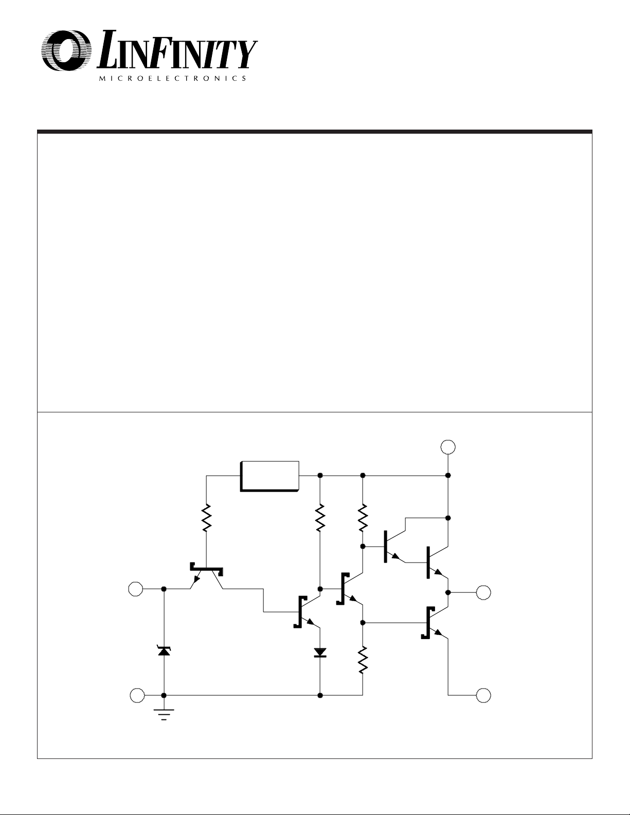
EQUIVALENT CIRCUIT SCHEMATIC
FEATURES
••
• Totem pole outputs with 3.0A peak current
••
capability.
••
• Supply voltage to 22V.
••
••
• Rise and fall times less than 25ns.
••
••
• Propagation delays less than 20ns.
••
••
• Non-inverting high-speed high-voltage Schottky
••
logic.
••
• Efficient operation at high frequency.
••
••
• Available in:
••
8 Pin Plastic and Ceramic DIP
14 Pin Ceramic DIP
16 Pin Plastic S.O.I.C.
20 Pin LCC
TO-99
TO-66
HIGH RELIABILITY FEATURES - SG1644
♦♦
♦ Available to MIL-STD-883
♦♦
♦♦
♦ Radiation data available
♦♦
♦♦
♦ LMI level "S" processing available
♦♦
V
CC
INV. INPUT
LOGIC
GND
(Substrate)
2.5K
6.5V
V
REG
3K3K
OUTPUT
POWER
GND
9/91 Rev 1.2 6/97 LINFINITY Microelectronics Inc.
Copyright 1997 11861 Western Avenue
1 (714) 898-8121
∞ ∞
∞ Garden Grove, CA 92841
∞ ∞
∞∞
∞ FAX: (714) 893-2570
∞∞

ABSOLUTE MAXIMUM RATINGS (Note 1)
SG1644/SG2644/SG3644
Supply Voltage (VCC) ...........................................................
Logic Input Voltage ...............................................................
Source/Sink Output Current (Each Output)
Continuous ...................................................................
Pulse, 500ns ................................................................
Note 1. Exceeding these ratings could cause damage to the device. All voltages are with respect to ground. All currents are positive into the
specified terminal.
22V
7V
±0.5A
±3.0A
Operating Junction Temperature
Hermetic (J, T, Y, R-Packages) ....................................
Plastic (M, DW, L-Packages) ......................................
Storage Temperature Range ............................
-65°C to 150°C
Lead Temperature (Soldering, 10 Seconds) ..................
THERMAL DATA
J Package:
Thermal ResistanceThermal Resistance-
Y Package:
Thermal ResistanceThermal Resistance-
M Package:
Thermal ResistanceThermal Resistance-
DW Package:
Thermal ResistanceThermal Resistance-
T Package:
Thermal ResistanceThermal Resistance-
Junction to Case, θ
Junction to Ambient, θ
Junction to Case, θ
Junction to Ambient, θ
Junction to Case, θ
Junction to Ambient, θ
Junction to Case, θ
Junction to Ambient, θ
Junction to Case, θ
Junction to Ambient, θ
JC
JC
JC
JC
JC
.................. 30°C/W
............... 80°C/W
JA
.................. 50°C/W
............. 130°C/W
JA
.................. 60°C/W
.............. 95°C/W
JA
.................. 40°C/W
............... 95°C/W
JA
.................. 25°C/W
............ 130°C/W
JA
R Package:
Thermal ResistanceThermal Resistance-
Junction to Case, θ
Junction to Ambient, θ
L Package:
Thermal ResistanceThermal Resistance-
Note A. Junction Temperature Calculation: TJ = TA + (PD x θJA).
Note B. The above numbers for θ
resistance of the package in a standard mounting configuration.
numbers are meant to be guidelines for the thermal
The θ
JA
performance of the device/pc-board system. All of the above
assume no ambient airflow.
Junction to Case, θ
Junction to Ambient, θ
are maximums for the limiting thermal
JC
................. 5.0°C/W
JC
.............. 40°C/W
JA
.................. 35°C/W
JC
............ 120°C/W
JA
RECOMMENDED OPERATING CONDITIONS (Note 2)
Supply Voltage (V
Frequency Range ...............................................
) ..................................
CC
4.5V to 20V (Note 3)
DC to 1.5MHz
Peak Pulse Current ............................................................
Logic Input Voltage .................................................
Note 2. Range over which the device is functional.
Note 3. AC performance has been optimized for V
-0.5 to 5.5V
= 8V to 20V.
CC
±3A
Operating Ambient Temperature Range (T
SG1644 .........................................................
)
A
SG2644 ...........................................................
SG3644 ...............................................................
-55°C to 125°C
-25°C to 85°C
0°C to 70°C
150°C
150°C
300°C
ELECTRICAL CHARACTERISTICS
(Unless otherwise specified, these specfiications apply over the operating ambient temperatures for SG1644 with -55°C ≤ TA ≤ 125°C, SG2644 with -25°C
≤ TA ≤ 85°C, SG3644 with 0°C ≤ TA ≤ 70°C, and VCC = 20V. Low duty cycle pulse testing techniques are used which maintains junction and case
temperatures equal to the ambient temperature.)
Test ConditionsParameter
Static Characteristics
Logic 1 Input Voltage
Logic 0 Input Voltage
Input High Current
Input High Current
Input Low Current
Input Clamp Voltage
Output High Voltage
(Note 4)
Output Low Voltage (Note 4)
Supply Current Outputs Low
Supply Current Outputs High
Note 4. VCC = 10V to 20V.
9/91 Rev 1.2 6/97 LINFINITY Microelectronics Inc.
Copyright 1997 11861 Western Avenue
VIN = 2.4V
= 5.5V
V
IN
V
= 0V
IN
= -10mA
I
IN
I
= -200mA
OUT
I
= 200mA
OUT
= 0V (both inputs)
V
IN
V
= 2.4V (both inputs)
IN
2 (714) 898-8121
SG1644/2644/3644
Min. Typ. Max.
2.0
0.7
500
1.0
-4
-1.5
V
-3
CC
1.0
18
27
7.5
12
∞ ∞
∞ Garden Grove, CA 92841
∞ ∞
∞∞
∞ FAX: (714) 893-2570
∞∞
Units
V
V
µA
mA
mA
V
V
V
mA
mA

ELECTRICAL CHARACTERISTICS (continued)
SG1644/SG2644/SG3644
Test Conditions (Figure 1)Parameter
SG1644/2644/3644
TA= 25
°°
°C
°°
Min. Typ. Max.
Dynamic Characteristics
Propagation Delay High-Low
(TPHL)
Propagation Delay Low-High
(TPLH)
Rise Time (TTLH)
Fall Time (TTHL)
Supply Current (I
(both outputs)
Note 5. These parameters, specified at 1000pF, although guaranteed over recommended operating conditions, are not tested in production.
Note 6. VCC = 15V.
)
CC
(Note 6)
CL = 1000pF (Note 5)
CL = 2500pF
= 1000pF (Note 5)
C
L
CL = 2500pF
= 1000pF (Note 5)
C
L
CL = 2500pF
C
= 1000pF (Note 5)
L
CL = 2500pF
C
= 2500pF, Freq. = 200KHz
L
Duty Cycle = 50%
26
18
30
30
30
30
35
25
30
30
40
25
40
35
SG1644
TA=-55
°°
°C to 125
°°
°°
°C
°°
Min. Typ. Max.
40
50
30
40
35
50
30
50
40
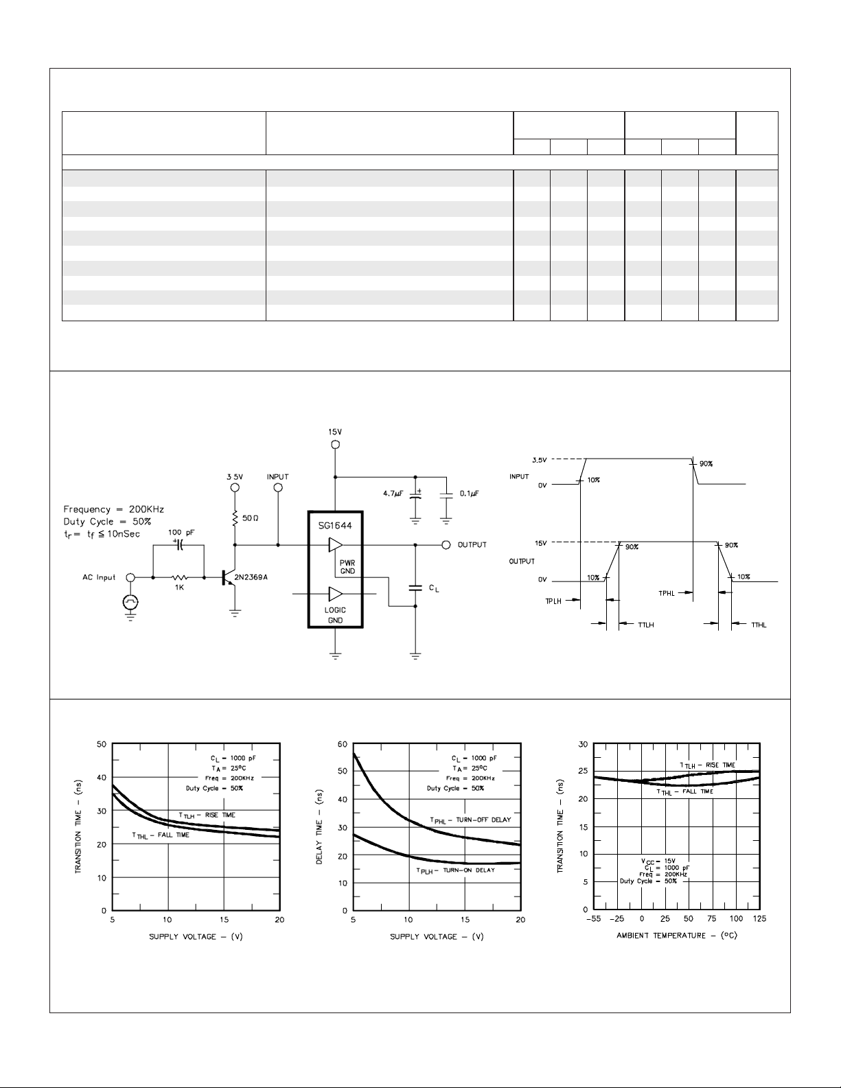
AC TEST CIRCUIT AND SWITCHING TIME WAVEFORMS - FIGURE 1
Units
ns
ns
ns
ns
ns
ns
ns
ns
mA
CHARACTERISTIC CURVES
FIGURE 2.
TRANSITION TIMES VS. SUPPLY VOLTAGE
9/91 Rev 1.2 6/97 LINFINITY Microelectronics Inc.
Copyright 1997 11861 Western Avenue
FIGURE 3.
PROPAGATION DELAY VS. SUPPLY VOLTAGE
3 (714) 898-8121
FIGURE 4.
TRANSITION TIMES VS. AMBIENT TEMPERATURE
∞ ∞
∞ Garden Grove, CA 92841
∞ ∞
∞∞
∞ FAX: (714) 893-2570
∞∞
 Loading...