

MXIC MX23C3210PC-10, MX23C3210TC-12, MX23C3210RC-12, MX23C3210MC-12, MX23C3210MC-10 Datasheet
...
MX23C3210
5 Volt 32-Mbit (4M x 8 / 2M x 16) Mask ROM
FEATURES
• Bit organization
- 4M x 8 (byte mode)
- 2M x 16 (word mode)
• Fast access time
- Random access: 100ns (max.)
• Current
- Operating:60mA
- Standby:100uA
• Supply voltage
- 5V±10%
• Package
- 44 pin SOP (500mil)
- 48 pin TSOP (12mm x 20mm)
- 42 pin DIP (600 mil) (word mode)
- 44 pin TSOP (Type II)
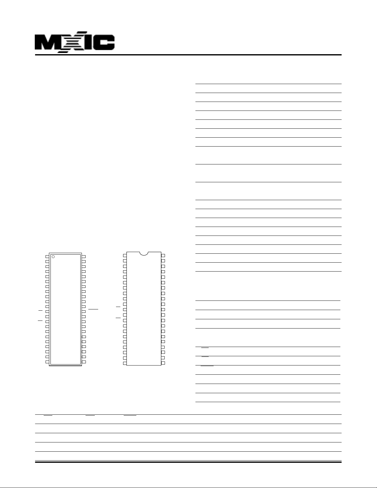
PIN CONFIGURATION
44 SOP/44 TSOP
NC
A18
A17
CE
VSS
OE
D10
D11
2
3
4
A7
5
A6
6
A5
7
A4
8
A3
9
A2
10
A1
11
A0
12
13
14
15
D0
16
D8
17
D1
18
D9
19
D2
20
21
D3
22
44
43
42
41
40
39
38
37
36
35
34
33
32
MX23C3210
31
30
29
28
27
26
25
24
23
42 DIP (For Word Mode Only)
A20
A19
A8
A9
A10
A11
A12
A13
A14
A15
A16
BYTE
VSS
D15/A-1
D7
D14
D6
D13
D5
D12
D4
VCC
A18
A17
A7
A6
A5
A4
A3
A2
A1
A0
CE
VSS
OE
D0
D8
D1
D9
D2
D10
D3
D11
MODE SELECTION
1
2
3
4
5
6
7
8
9
10
11
12
13
14
15
16
17
18
19
20
21
A19
42
A8
41
A9
40
A10
39
A11
38
A12
37
A13
36
A14
35
A15
34
A16
33
A20
32
VSS
31
D15
30
MX23C3210
D7
29
D14
28
D6
27
D13
26
D5
25
D12
24
D4
23
VCC
22
ORDER INFORMATION
Part No. Access Time Package
MX23C3210MC-10 100ns 44 pin SOP
MX23C3210MC-12 120ns 44 pin SOP
MX23C3210MC-15 150ns 44 pin SOP
MX23C3210TC-10 100ns 48 pin TSOP
MX23C3210TC-12 120ns 48 pin TSOP
MX23C3210TC-15 150ns 48 pin TSOP
MX23C3210RC-10 100ns 48 pin TSOP
(Reverse type)
MX23C3210RC-12 120ns 48 pin TSOP
(Reverse type)
MX23C3210RC-15 150ns 48 pin TSOP
(Reverse type)
MX23C3210PC-10 100ns 42 pin DIP
MX23C3210PC-12 120ns 42 pin DIP
MX23C3210PC-15 150ns 42 pin DIP
MX23C3210YC-10 100ns 44 pin TSOP
MX23C3210YC-12 120ns 44 pin TSOP
MX23C3210YC-15 150ns 44 pin TSOP
MX23C3210TI-10* 100ns 48 pin TSOP
MX23C3210TI-12* 120ns 48 pin TSOP
*Note: T emperature:-40°C~85°C
PIN DESCRIPTION
Symbol Pin Function
A0~A20 Address Inputs
D0~D14 Data Outputs
D15/A-1 D15 (Word Mode)/ LSB Address
(Byte Mode)
CE Chip Enable Input
OE Output Enable Input
Byte Word/ Byte Mode Selection
VC C Po wer Supply Pin
VSS Ground Pin
N C No Connection
CE OE Byte D15/A-1 D0~D7 D8~D15 Mode Po wer
H X X X High Z High Z - Stand-by
L H X X High Z High Z - Active
L L H Output D0~D7 D8~D15 Word Active
L L L Input D0~D7 High Z Byte Active
P/N:PM0247 REV. 3.2, SEP. 04, 2001
1
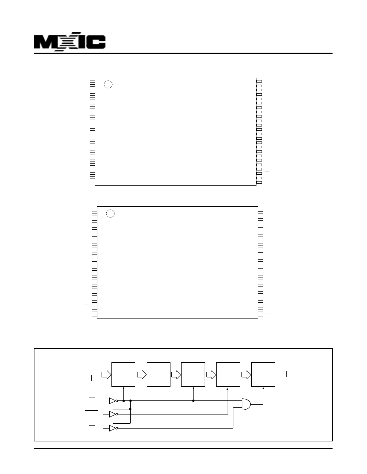
48 TSOP (Normal Type)
BYTE
A16
A15
A14
A13
A12
A11
A10
A9
A8
A19
VSS
A20
A18
A17
A7
A6
A5
A4
A3
A2
A1
A0
CE/CE
48 TSOP (Reverse Type)
MX23C3210
1
2
3
4
5
6
7
8
9
10
11
12
13
14
15
16
17
18
19
20
21
22
23
24
MX23C3210
(Normal T ype)
48
VSS
47
VSS
46
D15/A-1
45
D7
44
D14
43
D6
42
D13
41
D5
40
D12
39
D4
38
VCC
37
VCC
36
NC
35
D11
34
D3
33
D10
32
D2
31
D9
30
D1
29
D8
28
D0
27
OE/OE
26
VSS
25
VSS
VSS
VSS
D15/A-1
D7
D14
D6
D13
D5
D12
D4
VCC
VCC
NC
D11
D3
D10
D2
D9
D1
D8
D0
OE/OE
VSS
VSS
BLOCK DIAGRAM
A0/(A-1)
A20
48
47
46
45
44
43
42
41
40
39
38
37
36
35
34
33
32
31
30
29
28
27
26
25
Address
Buffer
MX23C3210
(Reverse Tp ye)
Memory
Array
Sense
Amplifier
Word/
Byte
1
2
3
4
5
6
7
8
9
10
11
12
13
14
15
16
17
18
19
20
21
22
23
24
Output
Buffer
BYTE
A16
A15
A14
A13
A12
A11
A10
A9
A8
A19
VSS
A20
A18
A17
A7
A6
A5
A4
A3
A2
A1
A0
CE/CE
D0
D15/(D7)
P/N:PM0247
CE
BYTE
OE
REV. 3.2, SEP. 04, 2001
2
MX23C3210
ABSOLUTE MAXIMUM RATINGS
Item Symbol Ratings
V oltage on any Pin Relativ e to VSS VIN -0.5V to 7.0V
Ambient Operating Temperature Topr -40°C to 85°C
Storage T emperature Tstg -65°C to 125°C
DC CHARACTERISTICS (Ta = -40°C ~ 85°C, VCC = 5V±10%)
Item Symbol MIN. MAX. Conditions
Output High Voltage VOH 2.4V - IOH = -1.0mA
Output Low Voltage VOL - 0.4V IOL = 2.1mA
Input High Voltage VIH 2.2V VCC+0.3V
Input Low Voltage VIL -0.3V 0.8V
Input Leakage Current ILI - 5uA 0V, VCC
Output Leakage Current ILO - 5uA 0V, VCC
Operating Current ICC1 - 60mA tRC = 100ns, all output open
Standby Current (TTL) ISTB1 - 1mA CE = VIH
Standby Current (cmos) ISTB2 - 100uA CE>VCC-0.2V
Input Capacitance CIN - 10pF Ta = 25°C, f = 1MHZ
Output Capacitance COUT - 10pF Ta = 25°C, f = 1MHZ
AC CHARACTERISTICS (Ta = -40°C ~ 85°C, VCC = 5V±10%)
Item Symbol 23C3210-10 23C3210-12 23C3210-15
MIN. MAX. MIN. MAX. MIN. MAX.
Read Cycle Time tR C 100ns - 120ns - 150ns Address Access Time tAA - 100ns - 120ns - 150ns
Chip Enable Access Time tACE - 100ns - 120ns - 150ns
Output Enable Time tOE - 50ns - 60ns - 70ns
Output Hold After Address tOH 0ns - 0ns - 0n s Output High Z Delay tHZ - 20ns - 20ns - 20ns
Note:Output high-impedance delay (tHZ) is measured
from OE going high, and this parameter guaranteed by
design over the full voltage and temperature operating
range - not tested.
P/N:PM0247
3
REV. 3.2, SEP. 04, 2001

AC T est Conditions
Note:
No output loading is present in tester load board.
Active loading is used and under software programming control.
Output loading capacitance includes load board's and all stray capacitance.
DOUT
C<100pF
IOL (load)=2.1mA
IOH (load)=-1mA
Input Pulse Levels 0.4V~2.4V
Input Rise and Fall Times 10ns
Input Timing Level 1.5V
Output Timing Le v el 0.8V and 2.0V
Output Load See Figure
TIMING DIAGRAM
RANDOM READ
MX23C3210
ADD
CE
OE
DATA
ADD ADD ADD
tAA
tRC
tOH
tACE
tOE
VALID VALID VALID
tHZ
P/N:PM0247
REV. 3.2, SEP. 04, 2001
4

PACKAGE INFORMATION
42-PIN PLASTIC DIP(600 mil)
MX23C3210
P/N:PM0247
REV. 3.2, SEP. 04, 2001
5

44-PIN PLASTIC SOP
MX23C3210
P/N:PM0247
REV. 3.2, SEP. 04, 2001
6

48-PIN PLASTIC TSOP
MX23C3210
P/N:PM0247
REV. 3.2, SEP. 04, 2001
7

44-PIN TSOP (Type II)
MX23C3210
P/N:PM0247
REV. 3.2, SEP. 04, 2001
8

MX23C3210
REVISION HISTORY
Revision Description Page Date
2.6 DC Characteristics: The input leakage current (ILI) is changed as 5uA
instead of 10uA.
The output leakage current (ILO) is changed as 5uA instead 10uA.
The power down supply current (ISTB2) is changed as 100uA instead of 5uA.
2.7 AC Characteristics: Added 100ns grade item, deleted 200ns grade item. MAR/25/1998
The output enable time (tOE) is changed as 60ns instead of 70ns in 120ns
grade item, and 70ns instead of 80ns grade item.
The output high Z delay is changed as 20ns instead of 70ns.
2.8 AC Characteristics: tOH 10ns --> 0ns P3 FEB/01/1999
2.9 T yping error correction P1 JAN/18/2000
3.0 Modify Package Inf ormation P5~7 JUL/17/2001
Added 44-pin TSOP(Type II) Pac kage P1,8
3.1 Added MX23C3210TI-10 & MX23C3210TI-12 in Order Information P1 JUL/31/2001
3.2 Change Ambient Operating Temperature:0°C to 70°C-->-40°C to 85°C P3 SEP/04/2001
P/N:PM0247
REV. 3.2, SEP. 04, 2001
9

MX23C3210
MACRONIX INTERNATIONAL CO., LTD.
HEADQUARTERS:
TEL:+886-3-578-6688
FAX:+886-3-563-2888
EUROPE OFFICE:
TEL:+32-2-456-8020
FAX:+32-2-456-8021
JAPAN OFFICE:
TEL:+81-44-246-9100
FAX:+81-44-246-9105
SINGAPORE OFFICE:
TEL:+65-348-8385
FAX:+65-348-8096
TAIPEI OFFICE:
TEL:+886-2-2509-3300
FAX:+886-2-2509-2200
MACRONIX AMERICA, INC.
TEL:+1-408-453-8088
FAX:+1-408-453-8488
CHICAGO OFFICE:
TEL:+1-847-963-1900
FAX:+1-847-963-1909
http : //www.macronix.com
MACRONIX INTERNATIONAL CO., LTD. reserves the right to change product and specifications without notice.
10
 Loading...