

Page 1
Service
VC8100 /U1B
Manual
PLAY MODE
STANDBY
POWER
ON/STANDBY
DIGITAL VIDEO
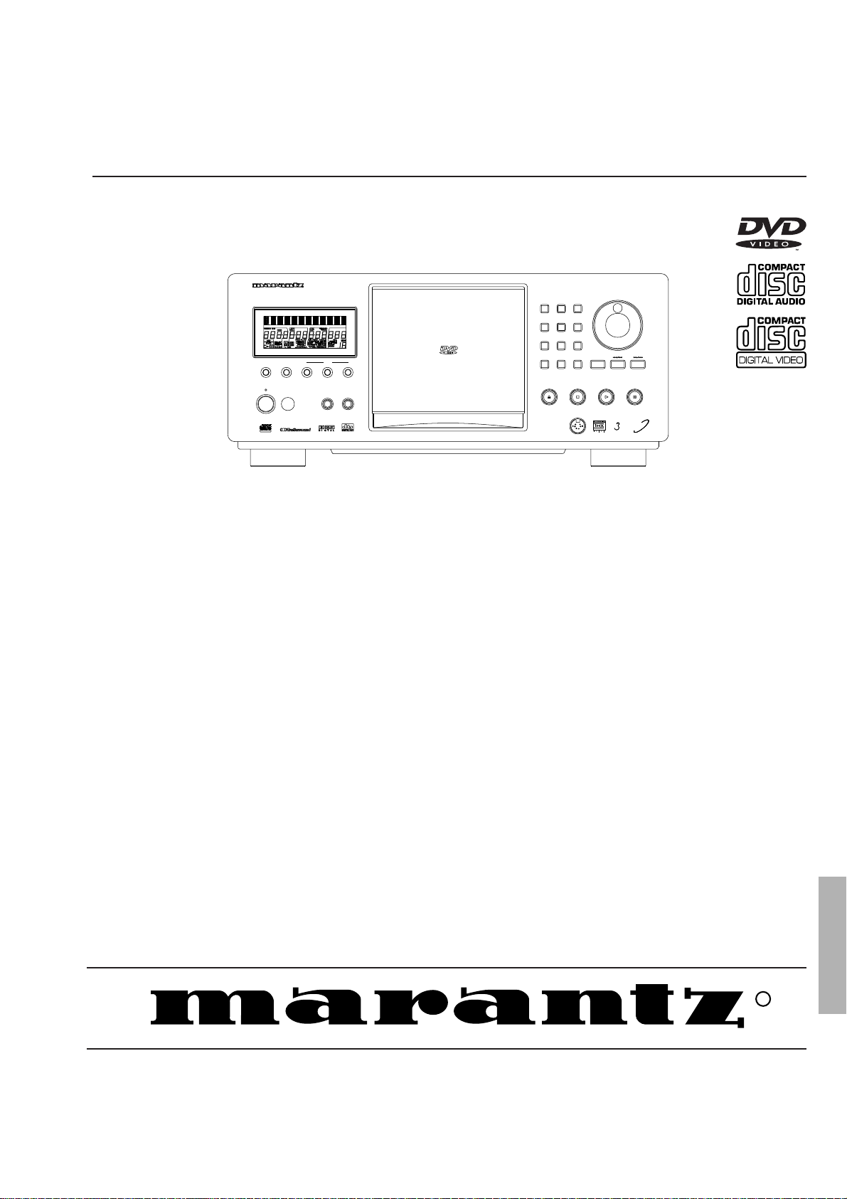
DVD CHANGER VC8100
RANDOM DISPLAY INPUT SEARCH
TEXT
SINGLE LOADER
ACCESS PLAY
KEYBOARD
/MOUSE
DISC/CHARADIRECT CUSTOM
PUSH ENTER
CLEAR
CC+1DVDCC+1DVDCC+1DVDCC+1DVDCC+1DVD
CC+1DVDCC+1DVD
CC+1DVDCC+1DVDCC+1DVD
CC+1DVD
CHANGER
CHANGER
CHANGER
CHANGER
CHANGER
CHANGERCHANGERCHANGER
CHANGERCHANGERCHANGER
CHANGERCHANGERCHANGER
CHANGERCHANGERCHANGER
CHANGERCHANGERCHANGER
CHANGERCHANGER
CHANGERCHANGER
CHANGERCHANGER
CHANGERCHANGER
CHANGERCHANGER
CHANGER
CHANGER
CHANGER
CHANGER
CHANGER
123
456
789
AUDIO/VIDEO UPDATE
10
OPEN/CLOSE STOP PLAY PAUSE
DVD Changer
TABLE OF CONTENTS
SECTION PAGE
1. SPECIFICATIONS...................................................................................................................................... 1
2. SAFETY INFORMATION............................................................................................................................ 2
3. SERVICING PRECAUTIONS ..................................................................................................................... 3
4. INFORMATIONS ........................................................................................................................................ 4
5. SERVICING HINT....................................................................................................................................... 5
6. REGIONAL CODES ................................................................................................................................... 6
7. EXPLODED VIEW AND PARTS LIST........................................................................................................ 7
8. BLOCK DIAGRAM AND SCHEMATIC DIAGRAM ................................................................................... 16
9. PCB CONNECTION DIAGRAM ............................................................................................................... 43
10. PCB PARTS LIST..................................................................................................................................... 59
11. ADJUSTMENT.......................................................................................................................................... 66
12. GENERAL INFORMATION ...................................................................................................................... 70
13. PANEL FACILITIES................................................................................................................................ 100
Please use this service manual with referring to the user guide (D.F.U) without fail.
VC8100
R
Printed in Japan
VC8100
296W855010 ACT
First Issue:2000.07
Page 2
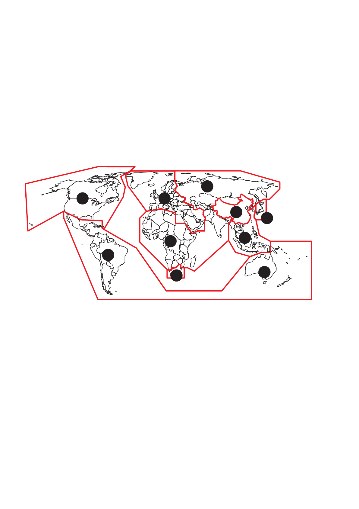
MARANTZ DESIGN AND SERVICE
MARANTZ AMERICA, INC.
Using superior design and selected high grade components, MARANTZ company has created the ultimate in stereo sound.
Only original
it is famous.
Parts for your
ORDERING PARTS :
Parts can be ordered either by mail or by Fax.. In both cases, the correct part number has to be specified.
The following information must be supplied to eliminate delays in processing your order :
1. Complete address
2. Complete part numbers and quantities required
3. Description of parts
4. Model number for which part is required
5. Way of shipment
6. Signature : any order form or Fax. must be signed, otherwise such part order will be considered as null and void.
MARANTZ parts can insure that your MARANTZ product will continue to perform to the specifications for which
MARANTZ equipment are generally available to our National Marantz Subsidiary or Agent.
USA
MARANTZ AMERICA, INC
440 MEDINAH ROAD
ROSELLE, ILLINOIS 60172
USA
PHONE : 630 - 307 - 3100
FAX : 630 - 307 - 2687
AMERICAS
SUPERSCOPE TECHNOLOGIES, INC.
MARANTZ PROFESSIONAL PRODUCTS
2640 WHITE OAK CIRCLE, SUITE A
AURORA, ILLINOIS 60504 USA
PHONE : 630 - 820 - 4800
FAX : 630 - 820 - 8103
AUSTRALIA
JAMO AUSTRALIA PTY LTD
1 EXPO COURT, P.O. BOX 350
MT. WAVERLEY VIC 3149
AUSTRALIA
PHONE : +61 - 3 - 9543 - 1522
FAX : +61 - 3 - 9543 - 3677
NEW ZEALAND
WILDASH AUDIO SYSTEMS NZ
14 MALVERN ROAD MT ALBERT
AUCKLAND NEW ZEALAND
PHONE : +64 - 9 - 8451958
FAX : +64 - 9 - 8463554
EUROPE / TRADING
MARANTZ EUROPE B.V.
P.O.BOX 80002, BUILDING SFF2
5600 JB EINDHOVEN
THE NETHERLANDS
PHONE : +31 - 40 - 2732241
FAX : +31 - 40 - 2735578
AUSTRALIA
TECHNICAL AUDIO GROUP PTY, LTD
558 DARLING STREET,
BALMAIN, NSW 2041,
AUSTRALIA
PHONE : 61 - 2 - 9810 - 5300
FAX : 61 - 2 - 9810 - 5355
THAILAND
MRZ STANDARD CO.,LTD
746 - 754 MAHACHAI ROAD.,
WANGBURAPAPIROM, PHRANAKORN,
BANGKOK, 10200 THAILAND
PHONE : +66 - 2 - 222 9181
FAX : +66 - 2 - 224 6795
TAIWAN
PAI- YUING CO., LTD.
6 TH FL NO, 148 SUNG KIANG ROAD,
TAIPEI, 10429, TAIWAN R.O.C.
PHONE : +886 - 2 - 25221304
FAX : +886 - 2 - 25630415
BRAZIL
PHILIP DA AMAZONIA IND. ELET. ITDA
CENTRO DE INFORMACOES AO
CEP 04698-970
SAO PAULO, SP, BRAZIL
PHONE : 0800 - 123123
FAX : +55 11 534. 8988
(Discagem Direta Gratuita)
CANADA
LENBROOK INDUSTRIES LIMITED
633 GRANITE COURT,
PICKERING, ONTARIO L1W 3K1
CANADA
PHONE : 905 - 831 - 6333
FAX : 905 - 831 - 6936
SINGAPORE
WO KEE HONG (S) PTE LTD
WO KEE HONG CENTRE
NO.23, LORONG 8, TOA PAYOH
SINGAPORE 319257
PHONE : +65 2544555
FAX : +65 2502213
MALAYSIA
WO KEE HONG ELECTRONICS SDN. BHD.
SUITE 8.1, LEVEL 8, MENARA GENESIS,
NO. 33, JALAN SULTAN ISMAIL,
50250 KUALA LUMPUR, MALAYSIA
PHONE : +60 3 - 2457677
FAX : +60 3 - 2458180
JAPAN
Technical
MARANTZ JAPAN, INC.
35- 1, 7- CHOME, SAGAMIONO
SAGAMIHARA - SHI, KANAGAWA
JAPAN 228-8505
PHONE : +81 42 748 1013
FAX : +81 42 741 9190
KOREA
MK ENTERPRISES LTD.
ROOM 604/605, ELECTRO-OFFICETEL, 16-58,
3GA, HANGANG-RO, YONGSAN-KU, SEOUL
KOREA
PHONE : +822 - 3232 - 155
FAX : +822 - 3232 - 154
SHOCK, FIRE HAZARD SERVICE TEST :
CAUTION : After servicing this appliance and prior to returning to customer, measure the resistance between either primary AC
cord connector pins ( with unit NOT connected to AC mains and its Power switch ON ), and the face or Front Panel of product and
controls and chassis bottom.
Any resistance measurement less than 1 Megohms should cause unit to be repaired or corrected before A C po w er is applied, and
verified before it is return to the user/customer.
Ref. UL Standard No. 1492.
In case of difficulties, do not hesitate to contact the Technical
Department at above mentioned address.
991207ACT
Page 3
1. SPECIFICATIONS
General
Power requirements ............................................... AC 120 V, 60 Hz
Power consumption ................................................................. 21 W
Power consumption in standby mode ..................... less than 0.9 W
Weight....................................................................8.0 kg (17.6 lbs.)
Dimensions ....................................440 (W) x 434 (D) x 193 (H) mm
(17 5/16 (W) x 17 1/8 (D) x 7 5/8 (H) in.)
Operating temperature ....................+5°C to +35°C
Operating humidity ........................... 5% to 85% (no condensation)
S-Video input/output
Y (luminance) - Output level .......................................1 Vp-p (75 Ω)
C (color) - Output level ........................................286 mVp-p (75 Ω)
Jacks........................................................................... S-VIDEO jack
Video input/output
Output level ................................................................. 1 Vp-p (75 Ω)
Jacks..................................................................................RCA jack
Component video output
(Y, PB, PR)
Output level .......................................................... Y: 1.0 Vp-p (75 Ω)
Jacks..................................................................................RCA jack
(+36°F to +96°F)
PB, PR: 0.7 Vp-p (75 Ω)
Digital output
Optical digital output ..........................................Optical digital jack
Coaxial digital input/output ................................................RCA jack
Control jacks
MASTER-SLAVE....................................................... Minijack (3.5 ø)
REMOTE CONTROL IN/OUT jack...................................... RCA jack
Other jacks
KEYBOARD/MOUSE jack .......................6-pin DIN connection jack
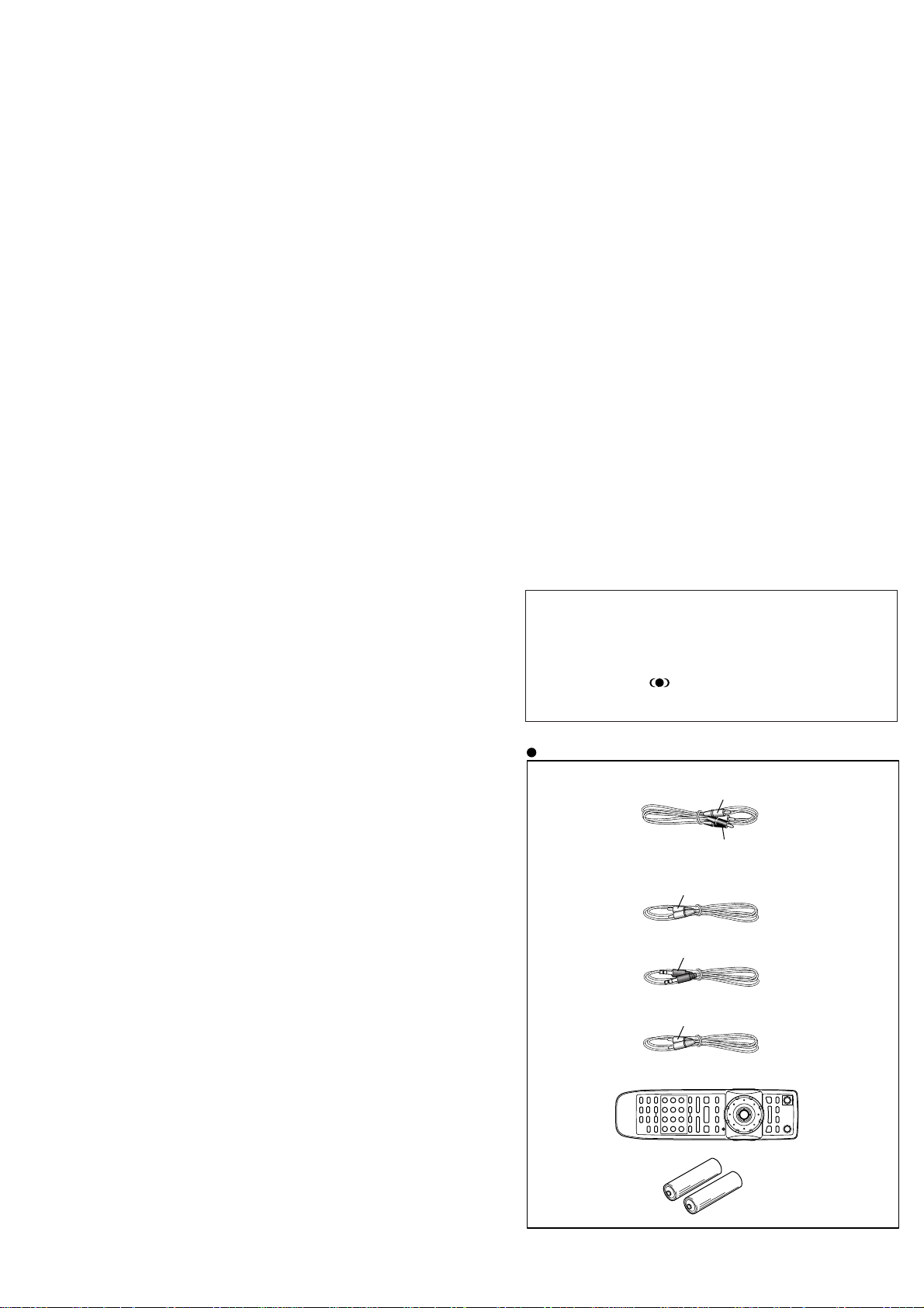
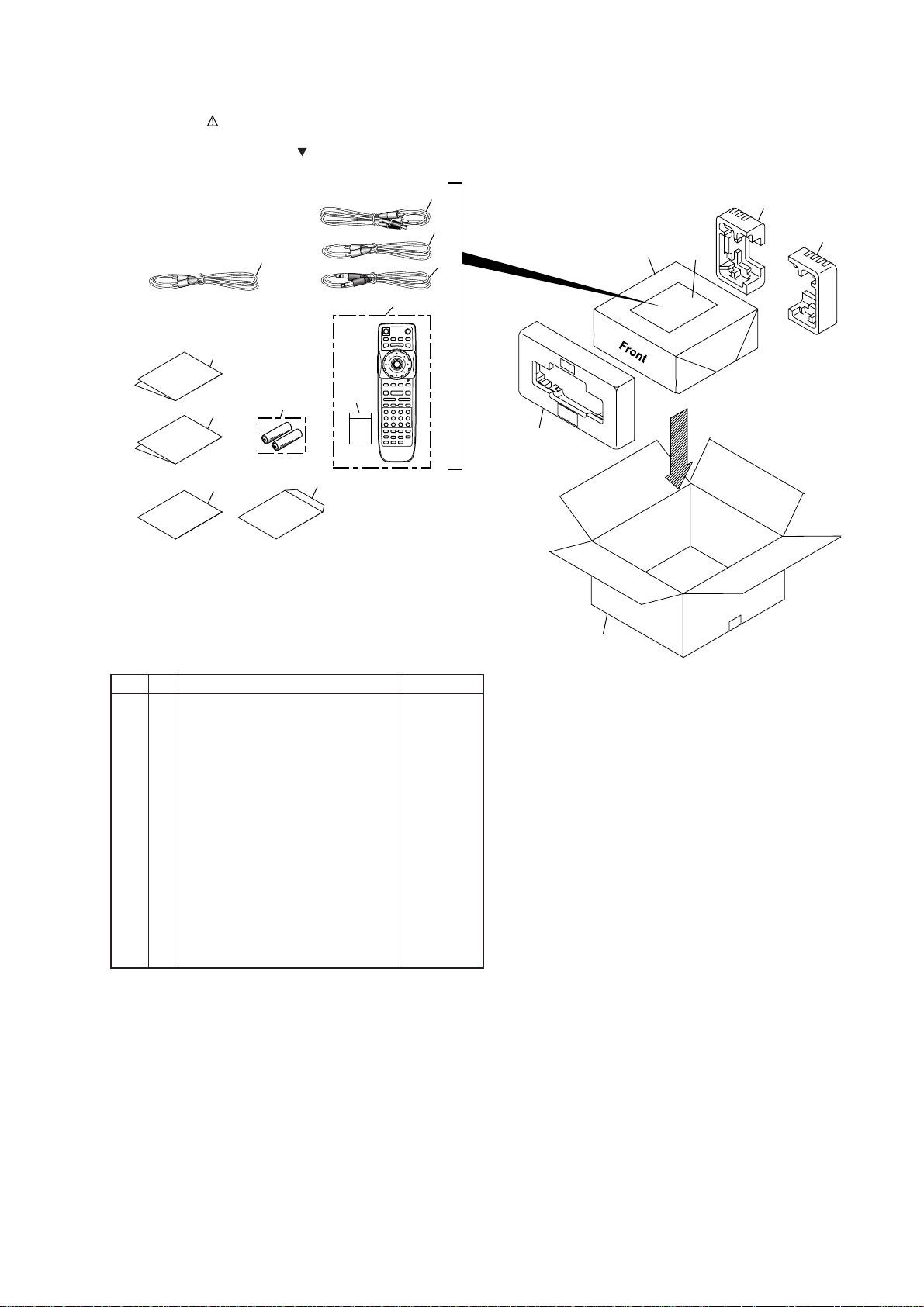
Accessories
Remote control unit .........................................................................1
AA (R6P) dry cell batteries .............................................................2
Audio cord ......................................................................................1
Video cord ......................................................................................1
D-Bus remote cord .........................................................................1
Master-Slave control cord...............................................................1
User guide (English x 1, French x 1) ..............................................2
Warranty Card ............................. (U.S. and Canadian models only)
Note
The specifications and design of this product are subject to change without
notice, due to improvement.
Audio input/output
Output level
During audio output ..............................200 mVrms (1 kHz, –20 dB)
Number of channels .......................................................................2
Jacks..................................................................................RCA jack
Digital audio characteristics
Frequency response..................... 4 Hz to 44 kHz (DVD fs: 96 kHz)
S/N ratio ...............................................................more than 115 dB
Dynamic range .................................................... more than 103 dB
Total harmonic distortion ..................................................... 0.002%
Wow and flutter .............................................. Limit of measurement
(±0.001% W. PEAK) or lower
• Manufactured under license from Dolby Laboratories. “Dolby” and the
double-D symbol are trademarks of Dolby Laboratories. Confidential
unpublished works. © 1992-1997 Dolby Laboratories. All rights
reserved.
• “DTS” is a trademark of Digital Theater Systems, Inc. Manufactured
under license from Digital Theater Systems, Inc.
• TruSurround and the
the United States and selected foreign countries. TruSurround
technology is incorporated under license from SRS Labs, Inc.
symbol are trademarks of SRS Labs, Inc. in
Accessories
Audio Cord (L = 1.5m)
White
Red
Video Cord (L = 1.5m)
Yellow
Master-Slave Control Cord (L = 0.75m)
D-BUS Remote Control Cord
Black
Orenge
Remote Control Unit (RC8100VC)
Dry Cell Battery (R6P, AA)
1
Page 4
2. SAFETY INFORMATION
This service manual is intended for qualified service technicians ; it is not meant for the casual doit-yourselfer. Qualified technicians have the necessary test equipment and tools, and have been
trained to properly and safely repair complex products such as those covered by this manual.
Improperly performed repairs can adversely affect the safety and reliability of the product and may
void the warranty. If you are not qualified to perform the repair of this product properly and safely,
you should not risk trying to do so and refer the repair to a qualified service technician.
WARNING
This product contains lead in solder and certain electrical parts contain chemicals which are known to the state of California to
cause cancer, birth defects or other reproductive harm.
NOTICE
(FOR CANADIAN MODEL ONLY)
Fuse symbols (fast operating fuse) and/or (slow operating fuse) on PCB indicate that replacement parts must
be of identical designation.
REMARQUE
(POUR MODÈLE CANADIEN SEULEMENT)
Les symboles de fusible (fusible de type rapide) et/ou (fusible de type lent) sur CCI indiquent que les pièces
de remplacement doivent avoir la même désignation.
(FOR USA MODEL ONLY)
Health & Safety Code Section 25249.6 – Proposition 65
1. SAFETY PRECAUTIONS
The following check should be performed for the
continued protection of the customer and service
technician.
LEAKAGE CURRENT CHECK
Measure leakage current to a known earth ground (water
pipe, conduit, etc.) by connecting a leakage current tester
such as Simpson Model 229-2 or equivalent between the
earth ground and all exposed metal parts of the appliance
(input/output terminals, screwheads, metal overlays,
control shaft, etc.). Plug the AC line cord of the appliance
directly into a 120V AC 60Hz outlet and turn the AC power
switch on. Any current measured must not exceed 0.5mA.
Reading should
not be above
0.5mA
Earth
ground
Device
under
test
Also test with
plug reversed
(Using AC adapter
plug as required)
AC Leakage Test
Leakage
current
tester
Test all
exposed metal
surfaces
ANY MEASUREMENTS NOT WITHIN THE LIMITS
OUTLINED ABOVE ARE INDICATIVE OF A POTENTIAL
SHOCK HAZARD AND MUST BE CORRECTED
BEFORE RETURNING THE APPLIANCE TO THE
CUSTOMER.
2. PRODUCT SAFETY NOTICE
Many electrical and mechanical parts in the appliance
have special safety related characteristics. These are
often not evident from visual inspection nor the
protection afforded by them necessarily can be obtained
by using replacement components rated for voltage,
wattage, etc. Replacement parts which have these
special safety characteristics are identified in this Service
Manual.
Electrical components having such features are identified
by marking with a
list in this Service Manual.
The use of a substitute replacement component which does
not have the same safety characteristics as the MARANTZ
recommended replacement one, shown in the parts list in
this Service Manual, may create shock, fire, or other
hazards.
Product Safety is continuously under review and new
instructions are issued from time to time. For the latest
information, always consult the current MARANTZ Service
Manual. A subscription to, or additional copies of,
MARANTZ Service Manual may be obtained at a nominal
charge from MARANTZ.
on the schematics and on the parts
2
Page 5

3. SERVICING PRECAUTIONS
CAUTION : Before servicing the DVD covered by this service
data and its supplements and ADDENDUMS, read and follow
the
SAFETY PRECAUTIONS. NOTE
circumstances create conflict between the following servicing
precautions and any of the safety precautions in this
publications, always follow the safety precautions.
: if unforeseen
Remember Safety First:
General Servicing Precautions
1. Always unplug the DVD AC power cord from the AC
power source before:
(1) Removing or reinstalling any component, circuit board,
module, or any other assembly.
(2) Disconnection or reconnecting any internal electrical
plug or other electrical connection.
(3) Connecting a test substitute in parallel with an elec-
trolytic capacitor.
Caution : A wrong part substitution or incorrect
polarity installation of electrolytic capacitors may result
in an explosion hazard.
2. Do not spray chemicals on or near this DVD or any of
its assemblies.
3. Unless specified otherwise in this service data, clean
electrical contacts by applying an appropriate contact
cleaning solution to the contacts with a pipe cleaner,
cotton-tipped swab, or comparable soft applicator.
Unless specified otherwise in this service data, lubrication
of contacts is not required.
4. Do not defeat any plug/socket B+ voltage interlocks with
which instruments covered by this service manual might
be equipped.
5. Do not apply AC power to this DVD and/or any of its
electrical assemblies unless all solid-state device heat
sinks are correctly installed.
6. Always connect test instrument ground lead to the
appropriate ground before connection the test instrument
positive lead. Always remove the test instrument ground
lead last.
Insulation Checking Procedure
Disconnect the attachment plug from the AC outlet and turn
the power on. Connect an insulation resistance meter(500V)
to the blades of the attachment plug. The insulation resistance
between each blade of the attachment plug and accessible
conductive parts (Note 1) should be more than 1M-ohm.
Note 1 : Accessible Conductive Parts including Metal panels,
Input terminals, Earphone jacks, etc.
Electrostatically Sensitive (ES) Devices
Some semiconductor (solid state) devices can be damaged
easily by static electricity. Such components commonly are
called Electrostatically Sensitive (ES) Devices. Examples of
typical ES devices are integrated circuits and some field effect
transistors and semiconductor chip components.
The following techniques should be used to help reduce the
incidence of component damage caused by static electricity.
1. Immediately before handling any semiconductor component or semiconductor-equipped assembly, drain off any
electrostatic charge on your body by touching a known
earth ground. Alternatively, obtain and wear a commercially available discharging wrist strap device, which
should be removed for potential shock reasons prior to
applying power to the unit under test.
2. After removing an electrical assembly equipped with ES
devices, place the assembly on a conductive surface such
as aluminum foil, to prevent electrostatic charge buildup or
exposure of the assembly.
3. Use only a GROUNDED-tip soldering iron to solder or
unsolder ES devices.
4. Use only an anti-static solder removal device. Some
solder removal devices not classified a “anti-static” can
generate electrical charges sufficient to damage ES
devices.
5. Do not use freon-propelled chemicals. These can
generate electrical charge sufficient to damage ES
devices.
6. Do not remove a replacement ES device from its protective package until immediately before you are ready to
install it. (Most replacement ES devices are packaged with
leads electrically shorted together by conductive foam,
aluminum foil, or comparable conductive material).
7. Immediately before removing the protective material from
the leads of a replacement ES device, touch the protective
material to the chassis or circuit assembly into which the
device will be installed.
Caution : Be sure no power is applied to the chassis or
circuit, and observe all other safety precautions.
8. Minimize bodily motions when handling unpackaged
replacement ES devices. (Normally harmless motion such
as the brushing together of your clothes fabric or the lifting
of your foot from a carpeted floor can generate static electricity sufficient to damage an ES device.)
3
Page 6
4. INFORMATIONS
REGION CODE
VERSION REGION CODE COUNTRY
/UXX 1 USA/CANADA
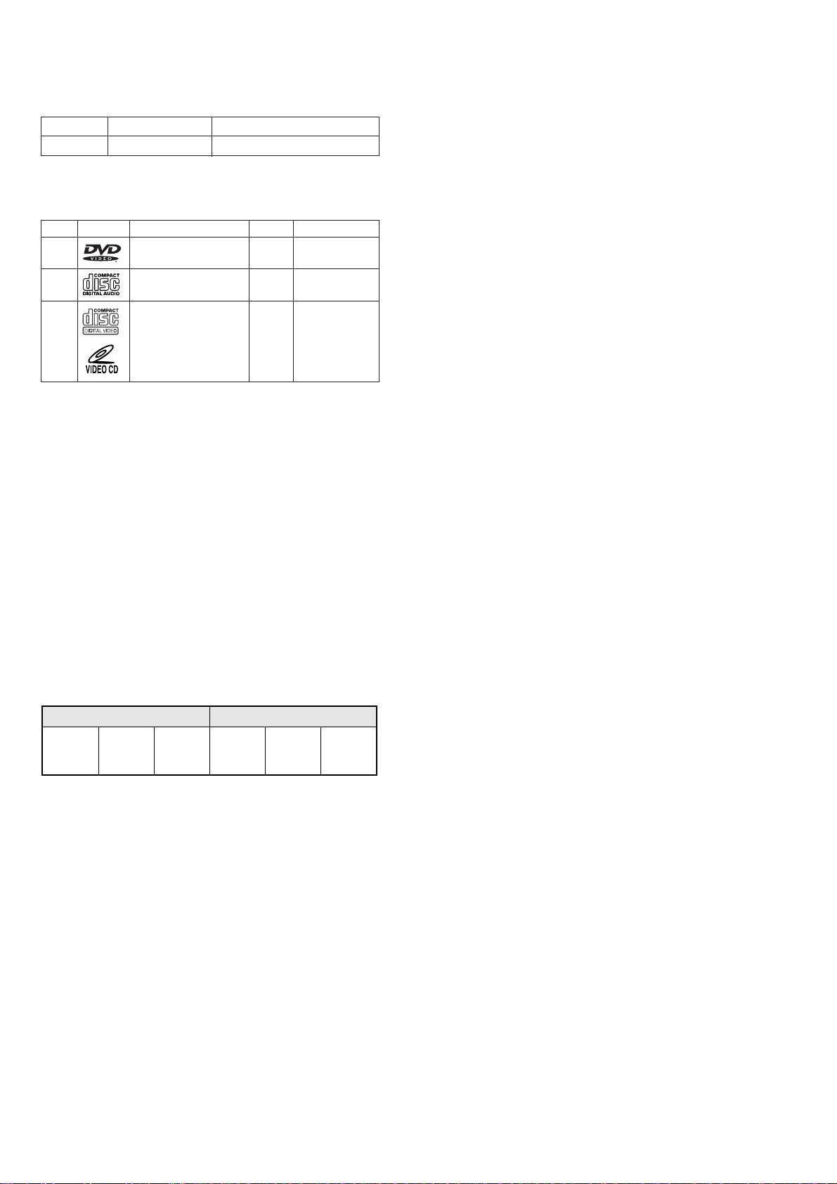
THE DISCS THAT THE DV8100 CAN HANDLE
The following discs can be played back with a DV8100.
disc mark playback capability size side
DVD Audio/Video
CD Audio
VCD Audio/Video single
Note: The regional code of the discs must meet to the regional
code of the DV8100.
12 cm
12 cm
12 cm
single/double
single
DVD INFORMATION
Below is a glossary of the new terms related to DVD.
Multi-angles:
On some DVDs, scenes have been filmed from different angles
(up to a maximum of 9). On these discs, you can select the
angle that you want to watch. Please refer to the DVD’s manual
to see which scenes have multi-angles.
Parental guide:
Some discs have restriction levels that allow you to cut scenes
or prevent playback of discs that have contents that you do
not want children to watch.
Title:
A disc may have more than one story/movie on it, so each
story/movie is called a “title”.
For example, if there are 2 movies on the disc, they are
separated into Title 1 and Title 2.
Chapter:
A title may also be separated into chapters.
For example, a movie (title) may be separated into 3 scenes
(chapters).
Title 1 Title 2
Chapter1Chapter
Subtitles:
DVDs are recorded with up to 32 different subtitle languages.
If a disc has more than one subtitle language, you can select
the subtitle language that you want to read.
Soundtrack language:
DVDs are recorded with up to 8 different soundtrack languages.
If a disc has more than one language, you can select the
soundtrack language that you want to listen to.
Chapter3Chapter1Chapter2Chapter
2
3
4
Page 7
5. SERVICING HINT
SERVICE HINTS
SERVICE TOOLS
Audio signals disc (SBC429) 4822 397 30184
Disc without errors (SBC444)+
Disc with DO errors, black spots and fingerprints (SBC444A) 4822 397 30245
Disc (65 min 1kHz) without no pause 4822 397 30155
Max. diameter disc (58.0 mm) 4822 397 60141
Torx screwdrivers
Set (straight) 4822 395 50145
Set (square) 4822 395 50132
13th order filter 4822 395 30204
DVD test disc 4822 397 10131
Service tool kit *VC8100JIG
– Test disc (GGV1025)
– Remote control unit for service (GGF1067)
– Interface (GGF1348)
– FFC (VDA1681)
5
Page 8
6. REGIONAL CODES
What are "regional codes"?
Motion picture studios want to control the home release of movies in different countries because theater releases arenít
simultaneous (a movie may come out on DVD in the US when itís just hitting screens in Europe). Therefore they have
required that the DVD standard include codes which can be used to lock out the playback of certain discs in certain geographical regions. Players sold in each region will have that regionís code built into the player. The player will refuse to play
these "region coded" discs which are not allowed in the region. However, regional codes are entirely optional. Discs without
codes will play on any player in any country. Some studios have already announced that only their new releases will have
regional codes. There are six regions:
1. United States and Canada
2. Europe and Japan
3. Far East (except Japan & China)
4. South America and Oceania
5. Africa and the Middle East
6. China (except Hong Kong)
5
1 2
6
2
5
3
4
2
Map of DVD Regions
4
6
Page 9
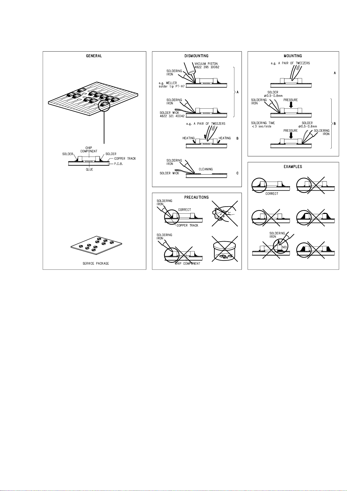
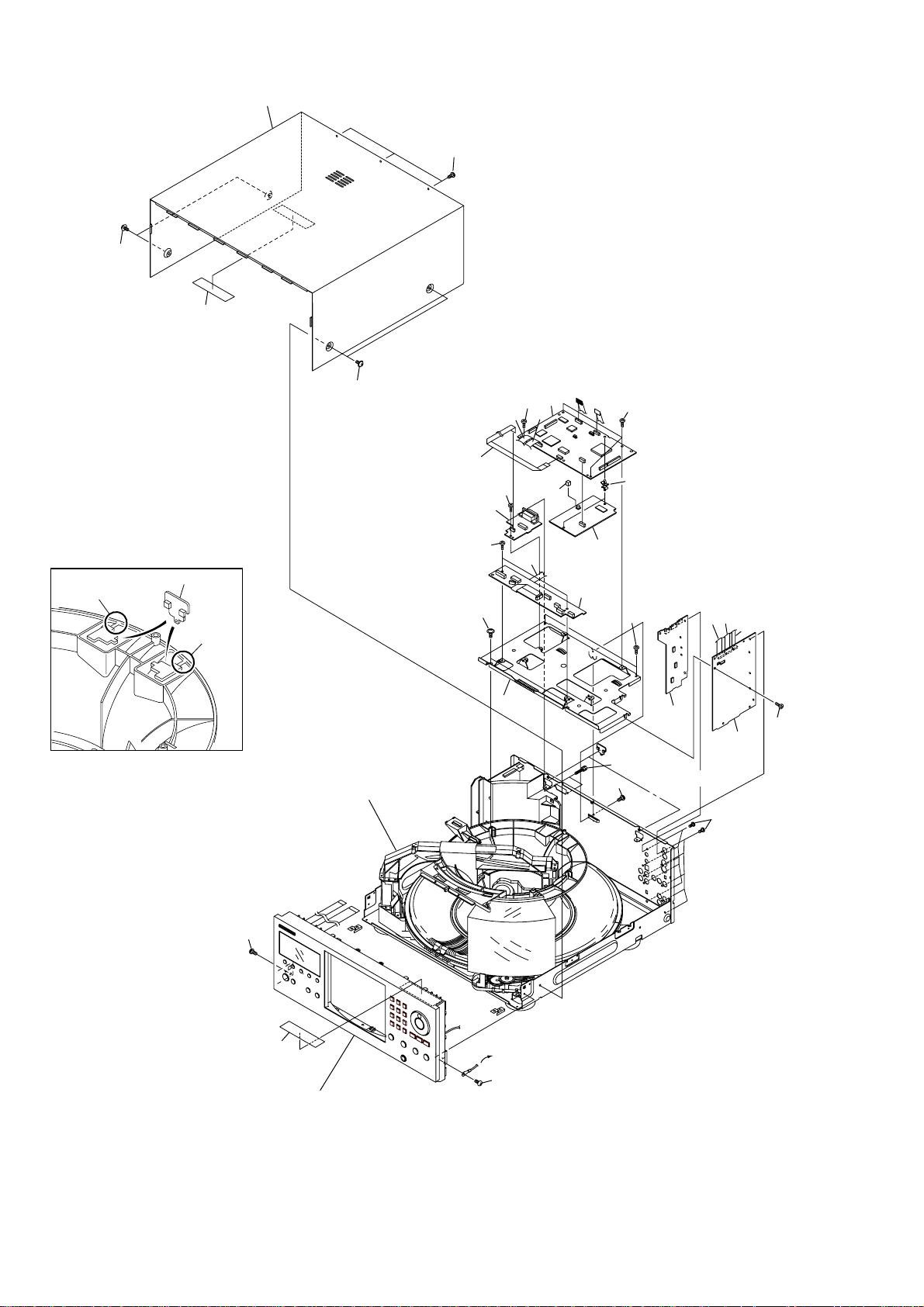
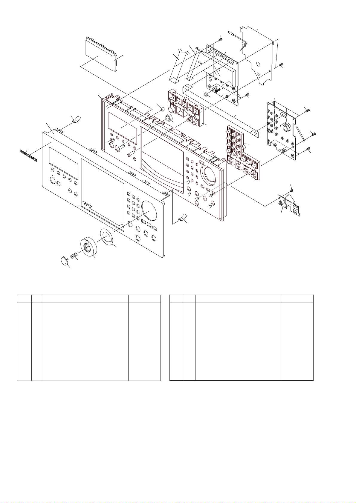
7. EXPLODED VIEWS AND PARTS LIST
NOTES:• Parts marked by "NSP" are generally unavailable because they are not in our Master Spare Parts List.
The mark found on some component parts indicates the importance of the safety factor of the part.
•
Therefore, when replacing, be sure to use parts of identical designation.
Screws adjacent to mark on the product are used for disassembly.
•
7.1 PACKING
13
15
6
16
(1) PACKING PARTS LIST
12
14
9
10
11
7
8
1
4
3
5
2 (1/2)
2 (2/2)
Mark No. Description Part No.
NSP 1 VHA1258, Protector F —
NSP 2 VHA1259, Protector R —
NSP 3 RHC1023, Packing Sheet —
NSP 4 VHG1914, Packing Case —
NSP 5 Z21-038, Polyethylene Bag B5 —
6 VRB1254, User Guide (English) 296W851250
7
VXX2709, Remote Control Unit RC8100VC
NSP 8 VNK4423, Battery Cover —
NSP 9 VDE1033, Audio Cord (L = 1.5m) —
NSP 10 VDE1034, Video Cord (L = 1.5m) —
NSP 11
NSP 12
NSP 13
NSP 14
NSP 16 092J854113, Warranty for USA —
RDE1023, Master-Slave Control Cord (L = 0.75m)
VEM-013, Dry Cell Battery (R6P, AA)
ZD00900100, D-BUS Remote control Cord
183J813502, Envelope Kit (Warranty for CANADA)
15 VRC1119, User Guide (French) 296W851260
ZK296W0010
—
—
—
—
7
Page 10
7.2 EXTERIOR SECTION (1/2)
23
28
22
29
Note ∗1
Cut
Part of Center Pole
Cut
28
Refer to
"7.3 EXTERIOR SECTION (2/2)".
8
30
29
1
29
10
9
29
2
17
15
7
29
16
3
6
29
4
∗1
14
29
29
1213
11
29
5
29
21
Refer to
"7.5 FRONT PANEL SECTION".
from PS2B Assy
29
8
Page 11

(1) EXTERIOR SECTION (1/2) PARTS LIST
Mark No. Description Part No.
1 VWS1396, DVDM Assy *ZZ001510R
NSP 2 VWG2201, 232B Assy —
NSP 3 VWV1669, VQEB Assy —
NSP 4 VWG2200, MSJB Assy —
NSP 5 VWV1720, AVJB Assy —
NSP 6 VWG2199, MDRB Assy —
NSP 7 VDA1779, Flexible Cable (12P) —
NSP 8 VDA1777, Flexible Cable (7P) —
NSP 9 VDA1781, Flexible Cable (11P) —
NSP 10 VDA1778, Flexible Cable (12P) —
NSP 11 VDA1782, Flexible Cable (7P) —
NSP 12 VDA1707, Flexible Cable (14P) —
NSP 13 VDA1784, Flexible Cable (15P) —
NSP 14 DBA1078, Screw (#4-40/M2) —
NSP 15 VEC2079, PCB Support Cushion —
NSP 16 VEC2077, PCB Spacer —
NSP 17 VNE2215, Main Holder —
NSP 21 VRW1817, Caution Label 301 —
NSP 22 ARW7050, 65 Label —
NSP 23 VXX2692, Bonnet Case S —
28 RBA1099, Screw 51260408M0
NSP 29 BBZ30P080FZK, Screw —
NSP 30 IPZ30P080FMC, Screw —
9
Page 12
7.3 EXTERIOR SECTION (2/2)
25
15
2
13
Note ∗3 :
KANTO KASEI FROIL PN-397 (for Service) : GYA1001
Note ∗4 :
KANTO KASEI HANARL PN-955R (for Service) : GEM1016
17
∗4
23
18
19
23
4
∗3
21
20
∗4
16
5
3
7
26
10
24
26
1
11
A
12
Refer to
"7.4 DISC RACK SECTION".
Note ∗2 (Screw Cover)
Part of Trans Cover (No.10)
10
Cut
24
24
22
5
26
28
27
27
28
24
14
A
∗2
24
8
9
24
24
10
Page 13

(1) EXTERIOR SECTION (2/2) PARTS LIST
Mark No. Description Part No. Mark No. Description Part No.
1 VWR1317, POWER SUPPLY Assy *ZZ001520R
NSP 2 VWG2197, LEDB Assy —
NSP 3 VWG2194, DOMB Assy —
NSP 4 VWG2195, DOSB Assy —
5 ADG7024, AC Power Cord *ZC000080R
6 VXM1033, Carriage Motor (DOOR) *MM001070R
7 VNK4630, Hood 296W162010
NSP 8 VNA2125, Under Base DVD —
9 PNW2766, Insulator 296W057010
NSP 10 VNK4542, Trans Cover —
NSP 11 VDA1776, Flexible Cable (26P) —
NSP 12 PNW2816, CR Lens —
NSP 13 VEC2113, Dispersion Sheet —
NSP 14 VNA2178, Rear Base —
NSP 15 PNW2792, Center Pole 301 —
16 PNW1634, Motor Pulley 296W262010
NSP 17 PNW2791, Hood Base 301 —
18 PNW2800, Gear M1 296W058010
19 PNW2906, Gear AW 296W058020
20 VNL1662, Gear Pulley 296W058030
21 PEB1300, Belt 296W264010
22 CM-22C, Cord Stopper 296W259010
NSP 23 IPZ20P080FMC, Screw —
NSP 24 BBZ30P080FZK, Screw —
NSP 25 IPZ30P080FMC, Screw —
NSP 26 PBA1106, Screw C —
NSP 27 296W160010, Earth Bracket —
NSP 28 IPZ20P080FMC, Screw —
11
Page 14
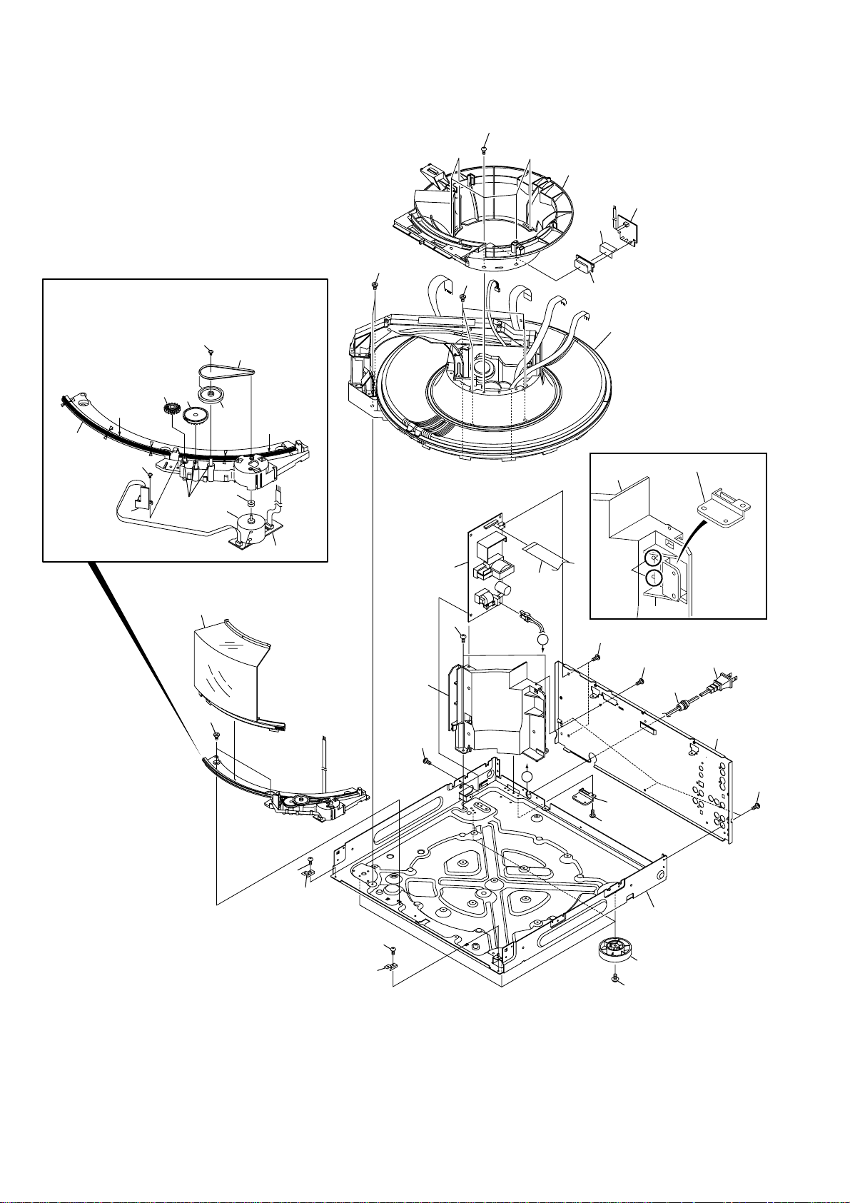
7.4 DISC RACK SECTION
52
53
B
52
Note ∗3 :
KANTO KASEI FROIL PN-397
(for Service) : GYA1001
Note ∗4 :
KANTO KASEI HANARL PN-955R
(for Service) : GEM1016
52
11
44
46
44
45
44
9
10
35
36
52
1
42
32
∗3
∗3
41
55
6
32
50
7
38
52
50
39
51
31
2
43
5
32
C
∗3
∗3
∗4
C
∗3
40
33
44
44
44
A
21
52
52
8
15
28
∗3
32
A
∗3
19
52
B
47
∗3
32
20
32
37
32
12
34
30
Page 15
●
DISC RACK SECTION PARTS LIST
Refer to
"7.6 TRAVERSE MECHANISM ASSY".
13
23
14
27
Note)
Tightening Torque: 2 kg·cm
9
10
49
4
16
a
∗
3
51
48
22
17
Mark No. Description Part No.
NSP 1 VWG2113, SSRB Assy
NSP 2 VWG2114, SEMB Assy
NSP 3 VWG2115, LOMB Assy
NSP 4 VWG2116, LOSB Assy
26
25
∗
3
24
54
51
14
b
29
b
12
a
18
∗
3
31
43
NSP 5 VWG2117, RADB Assy
NSP 6 VWG2118, PHOB Assy
NSP 7 VWG2196, VOLB Assy
8 VBH1318, Clamp Spring 296W115010
9 AEB7029, Loading Belt 296W264020
10 ANW7062, Gear Pulley (B) 296W058040
11 ANW7075, Roller B 296W358010
12 PBH1226, Drive Arm Spring 296W115020
NSP 13 VWT1161, Traverse Mechanism Assy
NSP 14 PED1028, Sheet 301
15 VXA2382, Clamper Assy 301 296W005500
16 PNW2819, Gear 1 296W058050
17 PNW2820, Gear 2 296W058060
NSP 18 PNW2822, Gear Holder
19 PNW2823, Slider Cam 296W054010
20 PNW2826, Clamp Pole” 296W272010
21 PNW2827, Clamper Holder 296W271010
22 PNW2829, Drive Arm 296W002010
23 AEB7063, Float Rubber A 296W130010
NSP 24 VNL1842, Balancer
NSP 25 VDA1785, Flexible Cable (8P)
26 VDA1780, Flexible Cable (24P) *YU000630R
27 VNL1841, Float Base 296W004010
28 PNW2844, Link L 296W121010
29 PNW2873, Drive Cam 296W054020
NSP 30 PNA2438, Lock Plate —
31 PNW1634, Motor Pulley 296W262010
32 PNW2647, Roller 296W358020
33 PNW2790, Disc Rack 296W064010
NSP 34 PNW2835, Rack Base —
35 PNW2836, ST Gear 0.6 296W058070
36 PNW2837, ST Gear 1.0 296W058080
NSP 37 PNW2838, Disc Divider —
NSP 38 PNW2839, Guide Support L —
NSP 39 PNW2840, Guide Support R —
NSP 40 PNW2841, Disc Guard —
NSP 41 PNW2842, Sensor Stay —
42 PNW2843, Guide Roller 296W358030
43
VXM1033, Carriage Motor (SELECT, LOADING)
44 PAM1770, Rack Label 296W861020
45 PAM1771, S Label 296W861030
46 PRW1507, +1 Label 296W861040
NSP 47 BBZ30P080FZK, Screw —
NSP 48 BMZ26P040FZK, Screw —
NSP 49 BPZ26P060FMC, Screw —
NSP 50 BPZ30P100FCU, Screw —
NSP 51 IPZ20P080FMC, Screw —
NSP 52 PPZ30P080FMC, Screw —
53 PXA1615, Arm Assy 296W002500
54 VBH1319, Float Spring 296W115030
NSP 55 IPZ30P080FMC, Screw —
*MM001070R
3
13
Page 16
7.5 FRONT PANEL SECTION
10
17
21
6
7
1
21
14
13
23
8
9
11
18
19
20
12
23
15
24
21
4
16
2
21
21
21
22
3
(1) FRONT PANEL SECTION PARTS LIST
Mark No. Description Part No. Mark No. Description Part No.
NSP 1 VWG2192, FLKY Assy —
NSP 2 VWG2193, KEYB Assy —
NSP 3 VWG2198, PS2B Assy —
NSP 4 VDA1839, Flexible Cable (11P) —
NSP 5 VDA1792, Flexible Cable (7P) —
NSP 6 VDA1786, Flexible Cable (7P) —
NSP 7 VDA1775, Flexible Cable (15P) —
8 296W248010, Front Panel 296W248010
9 185J251012, Marantz Badge 185J251010
10 296W158010, Display Window 296W158010
NSP 11 PEC1042, JOG Sheet —
12 296W355010, IR Lens 296W355010
13 PNW2019, LED Lens 296W355020
14 296W105010, Front Chassis 296W105010
15 296W270010, Mode Button 296W270010
16 296W270020, Play Button 296W270020
NSP 17 PNM1324, PCB Cover —
18 PAC1882, JOG Dial 296W067010
19 PBH1228, Enter Spring 296W115040
20 PAC1883, Enter Button 296W270050
NSP 21 PPZ30P080FMC, Screw —
NSP 22 PPZ30P050FMC, Screw —
NSP 23 VBK1128, Contactor —
NSP 24 296W120010, IR Filter —-
14
Page 17

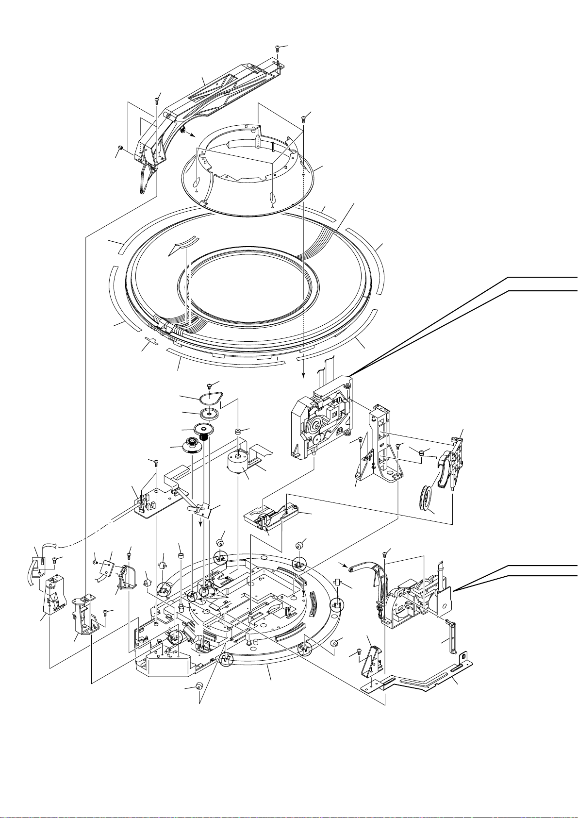
7.6 TRAVERSE MECHANISM ASSY
• Top View
37
18
26
11
25
27
7
29
36
3
22
33
21
33
23
28
10
15
10
5
10
13
37
10
14
7
2
7
18
32
1
35
30
16
*5
31
37
17
24
34
19
8
6
20
12
9
37
4
●
TRAVERSE MECHANISM ASSY PARTS LIST
Mark No. Description Part No. Mark No. Description Part No.
NSP 1 VWG2048, SMEB Assy —
NSP 2 VWG2009, FGSB Assy —
NSP 3 VXM1079, Motor —
NSP 4 VXM1078, Motor —
NSP
5 VWY1055, Pickup Assy —
NSP 6 DEC2040, Table Sheet —
NSP 7 VBA1058, Screw —
NSP 8 VBH1278, Centering Spring —
9 VBH1317, Hook Spring 296W115050
10 VBH1303, Skew Spring 296W115060
11 VBH1308, Gear Spring 296W115070
NSP 12 VEC1959, Reflected Sheet —
NSP 13 VLL1504, Guide Bar —
NSP 14 VLL1505, Sub-guide Bar —
15 VNC1017, Hold Spring 296W115080
NSP 16 VNE2070, Magnet Holder —
NSP 17 VNE2154, Motor Base —
NSP 18 VNE2155, Cover —
NSP 19 VNL1746, Centering Ring —
NSP 20 VNL1747, Disc Table —
21 VNL1770, Hook 296W258010
NSP 22 VNL1802, FFC Holder —
NSP 23 VNL1806, Mechanism Base —
NSP 24 VNL1807, FG Holder —
25 VNL1808, Gear A 296W058090
26 VNL1809, Gear B 296W058100
27 VNL1810, Gear C 296W058110
28 VNL1811, Slider 296W125010
NSP 29 VNL1814, Gear D —
NSP 30 VYM1024, Magnet —
NSP 31 JFZ17P025FZK, Screw —
NSP 32 JGZ17P028FMC, Screw —
NSP 33 VBA1051, Screw —
NSP 34 VXX2507, Magnet Holder Assy —
35 VXX2649, Spindle Motor Assy *ZK000290R
36 VXX2650, Carriage Motor Assy *ZK000300R
NSP 37 PBA1069, Screw —
*5 VXX2653, Traverse Mechanism Assy
(for Service)
*ZK000310R
15
Page 18
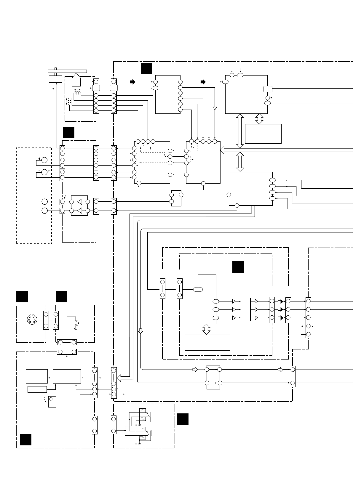
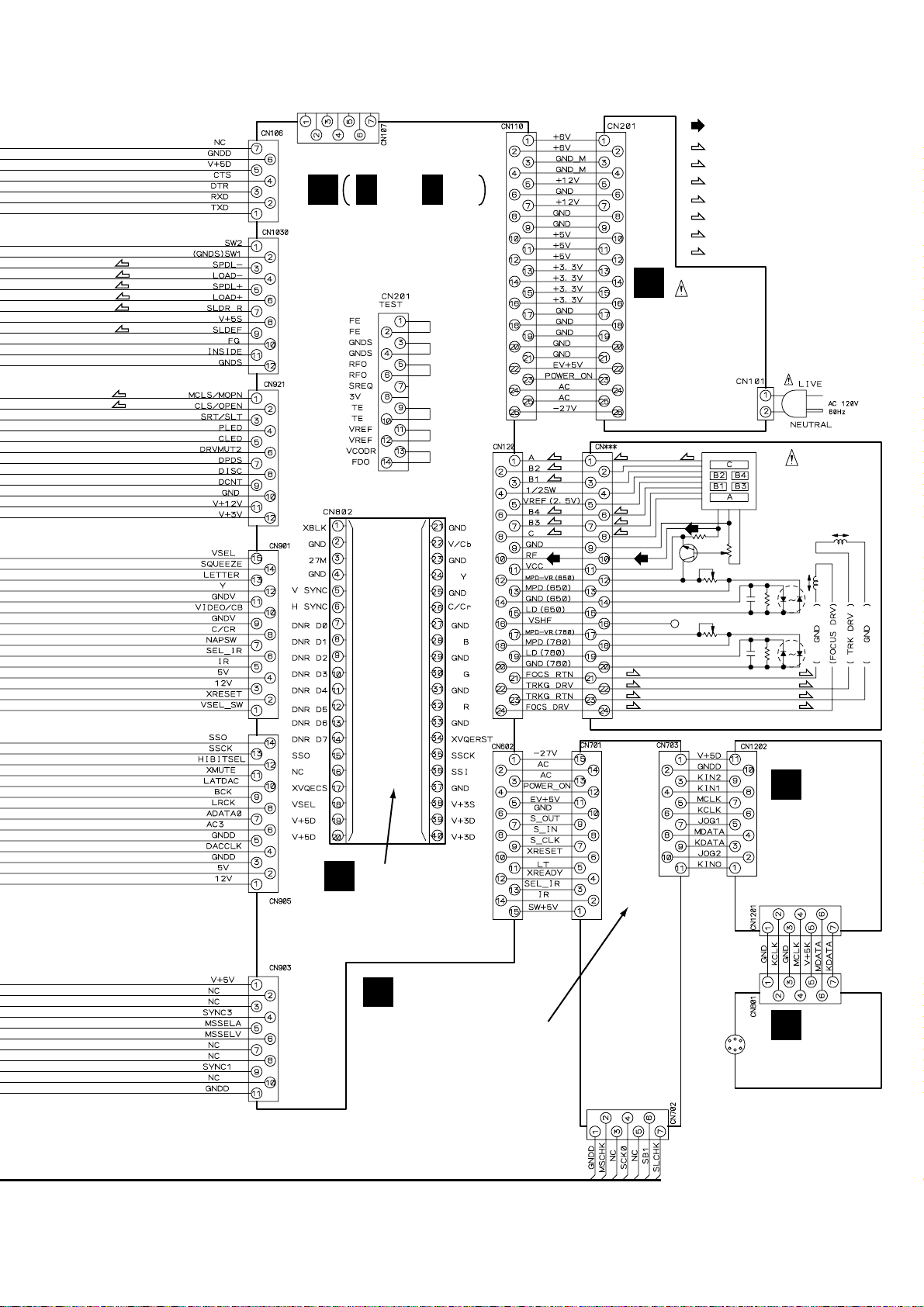
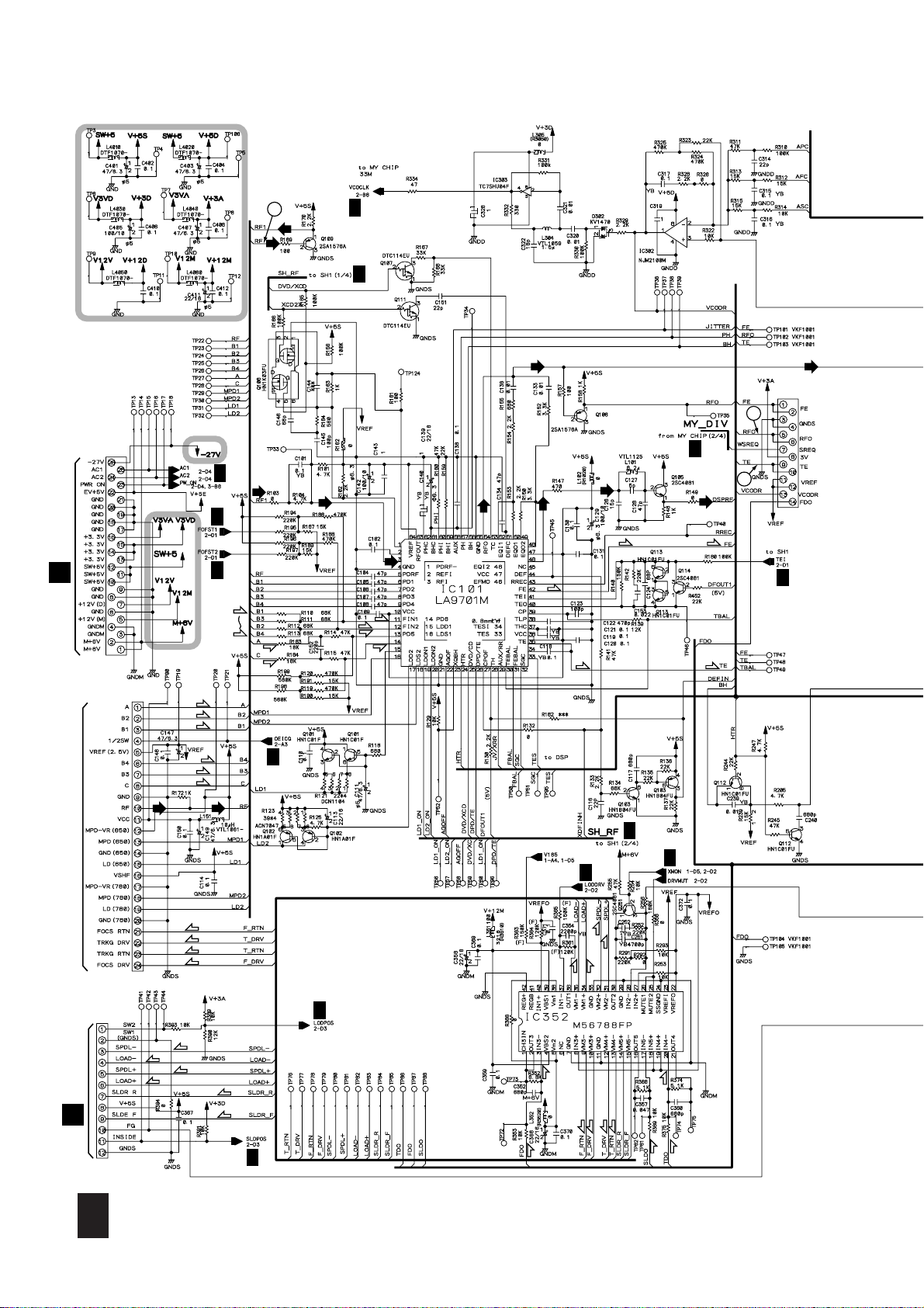
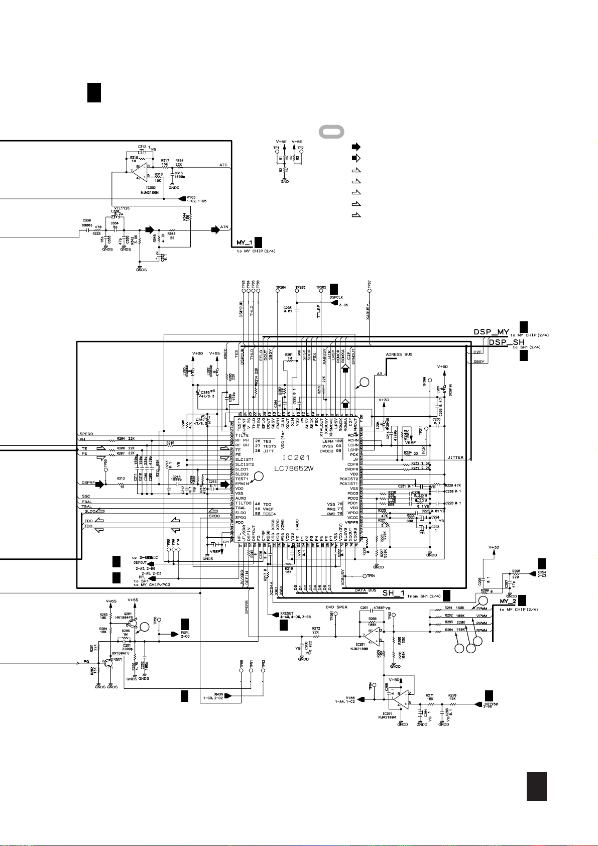
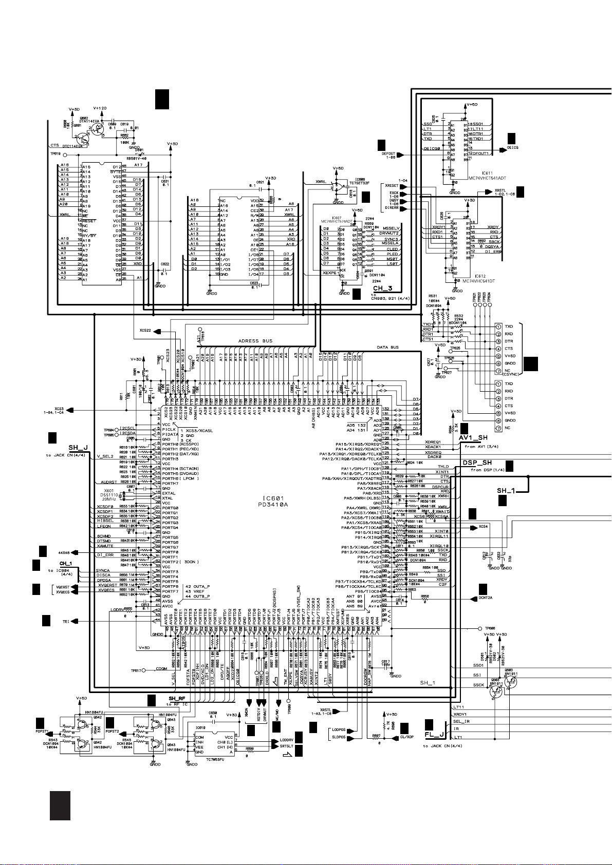
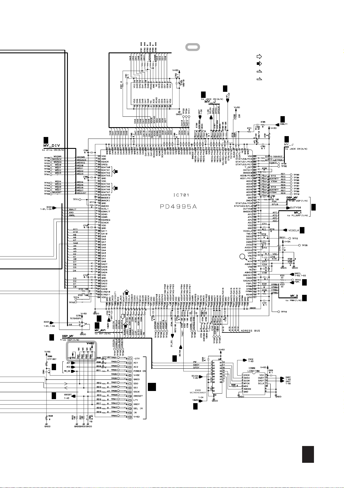
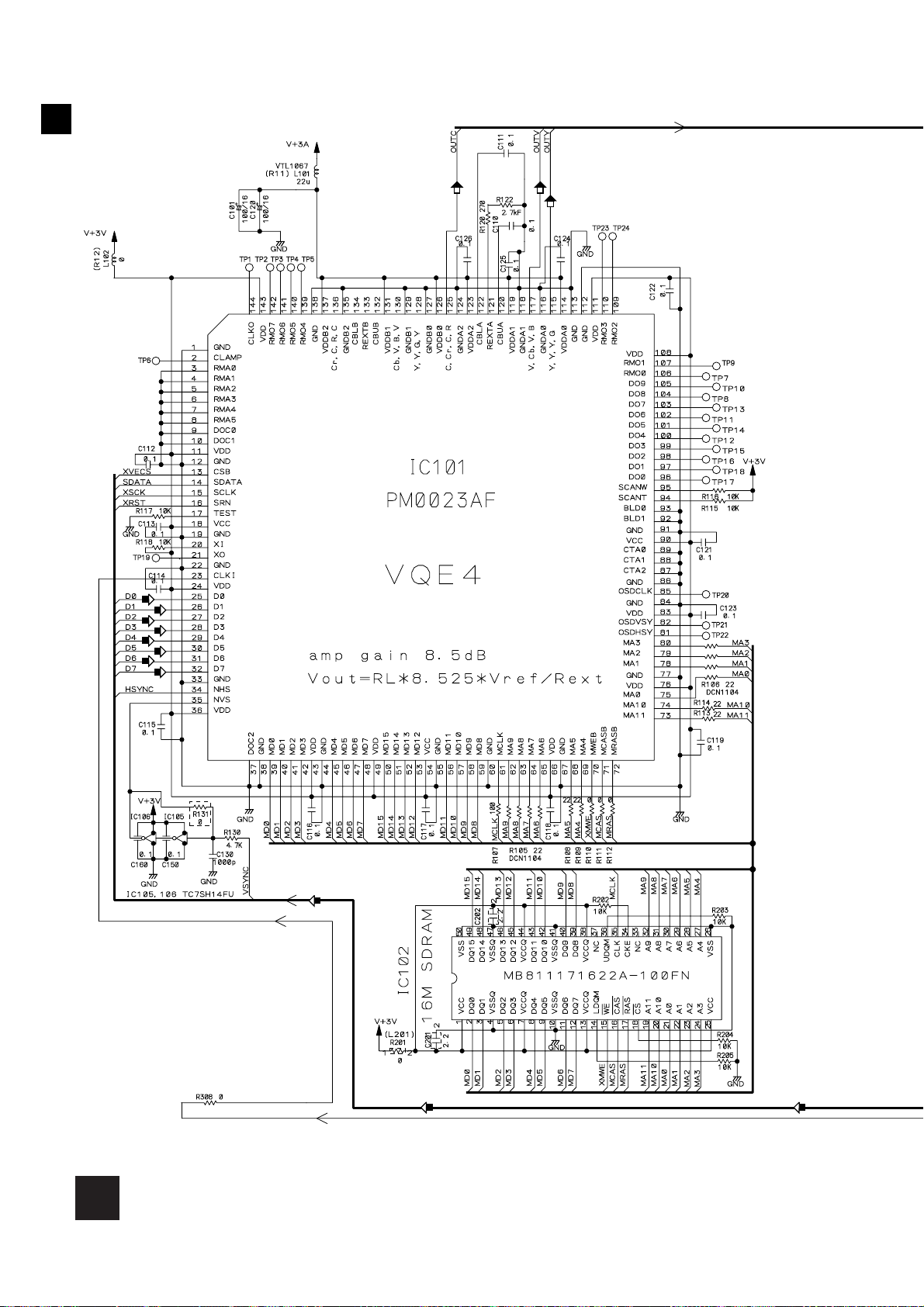
8. BLOCK DIAGRAM AND SCHEMATIC DIAGRAM
8.1 BLOCK DIAGRAM
CARRIAGE
MOTOR
LOADING
MOTOR
SELECT
MOTOR
DOOR
MOTOR
M
M
M
M
301 CHANGER
MECHANISM
SPDL
MOTOR
Q
CN303
7
8
5
3
2
1
CN305
(4P)
CN304
8
4
CN307
(9P)
MOTOR DRIVER
OEIC
FCS
TRKG
PICKUP
ASSY
MDRB
ASSY
(8P)
(5P)
14
SELECT DOOR
3
IC301
LA6531
(12P)
CN302
7
9
(24P)
10
7,6,
3,2
21
24
22
23
10
10
12
8
6
4
7
9
F_RTN
F_DRV
T_DRV
T_RTN
(12P)
CN301
SPDL+
SPDL-
SLDR_R
SLDR_F
LOAD+
LOAD-
SRT/
SLT
MCLS/
MOPH
(24P)
CN120
10
7,6,
3,2
21
24
22
23
(12P)
CN1030
5
3
7
9
6
4
(12P)
CN921
3
1
M
B1-B4
13 12 10 9
31
32
14
15
SPDL & FTS
34
35
37
LODDRV
DVDM ASSY
RFRF
3 54
RF IC
6-9
IC101
LA9701M
3
20
17
DRIVER
IC352
M56788FP
28
SLDO
SPDO
8
RFO
DSPRF
46
56
57
42
35
FDO
47
TDO
48
45
46
17
IC610
TC7W53FU
BH
PH
FE
TE
32 33 30 31 39
SERVO DSP
IC201
LC78652W
14
16M
170
Q105
33M 16M
107
4
DVD
DECODER
MY CHIP
IC701
PD4995A
MN414800CSJ-07
SYSTEM
CONTROL CPU
SH1 BASE ASIC
IC601
42
PD3410A
88
57-60
63-66
56
111
4M DRAM
IC702
SD0-SD7
SREQ
CDDATA
118
102
101
117
DTR
TXD
RXD
CTS
PS2B
U
ASSY
JA801
KEYBOARD
/MOUSE
FL TUBE
V701
VAW1052
KEY SW
REMOTE
SENSOR
S
FLKY ASSY
CN801
CN703
KEYB
T
ASSY
1
CN1201
717
1 11
1 11
FL CONTROL
IC701
PE5184A
CN1202
(15P)
CN701
(7P)
CN702
VIDEO ENCODER
(6ch, DNR)
IC101
CN802
CN101
-1/2
-1/2
7
27
(Y0-Y7) D0-D7
DNR
D0-D7
14
34
PM0023AF
25-32
117
115
125
OUTV
OUTY
OUTC
16M SDRAM
IC102
MB811171622A-100FN
(15P)
CN602
SEL IR
IR
SCK0
SB1
1
12
13
14
(7P)
CN903
4
2
SEL IR
IR
CN904
MASTER
CN905
SLAVE
P
MSJB ASSY
(1/2)
15
4
3
2
4
2
7 14
164
IC807
MC74VHCT541ADT
Q541
Q551
Q531
N
FILTER
VQEB
ASSY
VIDEO
F102
Q542
Q552
Q532
CN101
-2/2
2
4
6
(V)
(Y)
(C)
CN802
-2/2
22
24
26
CN901
SEL IR
CN905
7
6
(15P)
V
Y
C
IR
(14P)
ADATA0
ADAI (AC3)
10
12
8
6
5
16
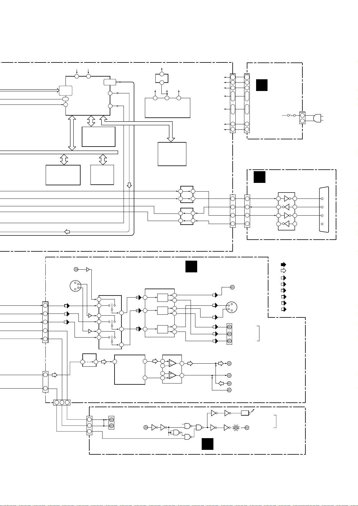
Page 19
149,150,
152-155,
158,159
162
48
WORK SRAM
(1M)
IC604
TC55V1001AF8
27M
36/16M
55 64
MPEG2
DECODER
MITUBISHI
AV-1
IC801
M65773AFP
16M SDRAM
MB811171622A
IC802
-100FN
FLASH
MEMORY
IC603
VYW1701
95-98,
100-103
71
74
YCBR0-7
(Y0-Y7)
AD0
DOUT0
16M
5
IC22
TC7WH74FU
1
27M
33M
36/16M
6
5
1
CLOCK GENERATOR
IC21
CY2081SL-655
EDO DRAM
IC803
M5M4V18165
DTP-6S
IC611
MC74VHCT541ADT
4
16
IC612
MC74VHC541DT
(26P)
CN110
M + 6V
+12V
+12V
+5V
+3.3V
E+5V
– 27V
16
155
4
515
(7P)
CN106
(26P)
CN201
1,2
1,2
5
5
7
7
10
|
POWER
12
SUPPLY
13
|
ASSY
16
22
26
R
(7P)
CN401
7
6
5
4
V
232B ASSY
MAX232EPE
10
9
11
12
IC401
CN101
7
8
14
13
LIVE
1
2
NEUTRAL
JA401
INTERFACE
CONNECTOR
2
3
4
14
AC IN
10
|
12
13
|
16
22
26
TXD
1
RXD
2
DTR
3
CTS
4
COMPOSITE
VIDEO IN
S VIDEO
IN
(15P)
CN501
(V/Cb)
6
4
(C/Cr)
8
10
11
(14P)
CN101
8
AC3/PCM
9
6 3 4
JA504
(2/2)
O
1
7
IC922
AVJB ASSY
JA504
(1/2)
(V)
CN503
(1/2)
(Y)
6
8
(C)
(C/Cr)
(V/Cb)
P
JA505
(Y)
JA201
L
R
L
R
IC901
MSJB ASSY (1/2)
COMPOSITE
VIDEO OUT
S VIDEO
OUT
R
(RED)
P
PB (BLUE)
Y (GREEN)
AUDIO
OUT
AUDIO
IN
ANALOG
COMPONENT
VIDEO
OUT
OPTICAL AC-3/PCM
COAXIAL
CN503
(2/2)
1
3
(Y)
Hi-bit
14 8
PD0236AM
CN502
(7P)
VIDEO
SELECTOR
IC502 BU4551BF
11
12
15
1
6
10
IC241
(7P)
CN902
4
5
2
DIN
JA989
2
(V/Cb)
(C/Cr)
13
14
5
96k,24-bit
2ch DAC
IC201
PE8001A
IN Remote
OUT Control
3IN 6OUT
VIDEO AMP
IC501 LA7135AM
AIN
3
BIN
6
(Y)
CIN
10
VOUTL
16 2
VOUTR
13
COAXIAL
IN
IC931
AMP
AMP
AMP
BA4560F
3
5
6
23
21
19
17
15
13
IC203
DIGITAL
SELECTOR
: RF Signal Route
: Audio Signal Route (L ch)
(V/Cb)
: V Signal Route
(Y)
: Y Signal Route
(C/Cr)
: C Signal Route
(R)
: R Signal Route
(G)
: G Signal Route
(B)
: B Signal Route
DIGITAL
AUDIO
OUT
17
Page 20
8.2 FGSB, SMEB, SSRB, SEMB, LOMB, LOSB, RADB, PHOB, DOMB, DOSB,
VOLB, LEDB, PICKUP ASSYS and OVERALL WIRING DIAGRAM
FGSB ASSY
A
(VWG2009)
CN201
52044-0345
CARRIAGE
MOTOR
ASSY
VXX2656
CN203
SPINDLE
MOTOR
ASSY
VXX2649
DOSB ASSY
J
(VWG2195)
(S)
LEDB ASSY
(VWG2197)
S201
DSG1016
(S)
(SP)
J632
L
CN202
VKN1212
(S)
(S)
(SP)
(SP)
B
DOMB ASSY
I
(VWG2194)
J632
SMEB ASSY
(VWG2048)
J631
(D)
J1601
(S)
(S)
(SP)
(SP)
(D)
R
232B ASSY
(VWG2201)
(SP)
(L)
(SP)
(L)
(S)
(S)
(D) (D)
(SP)
(SP)
(S)
(S)
(SL)(SL)
(L)
(L)
LOMB ASSY
E
(VWG2115)
LOSB ASSY
F
(VWG2116)
LEAF SW
C
SSRB ASSY
(VWG2113)
J652
VOLB ASSY
K
(VWG2196)
CN605
J605J603
J651
CN604
LED
HOLDER
RNK1795
(D)
(L)
(L)
H
PHOB ASSY
(VWG2118)
J604
G
RADB ASSY
(VWG2117)
J601
Q
MDRB ASSY
(VWG2199)
O 1/2, O 2/2
O
AVJB ASSY
(VWV1720)
P
MSJB ASSY
(VWG2200)
SEMB ASSY
(VWG2114)
D
J602
(SL)
(SL)
ININOUT
OUT
REMOTE
CONTROL
INTERNAL
REMOTE
CONTROL SW
EXTERNAL
A B C D E F G H I J K L
18
Page 21
Note : When ordering service parts, be sure to refer to "EXPLODED VIEWS and PARTS LIST" or "PCB PARTS LIST".
: RF SIGNAL ROUTE
(F)
: FOCUS SERVO LOOP LINE
(T)
: TRACKING SERVO LOOP LINE
(S)
: SLIDER SERVO LOOP LINE
V
(SP)
: SPINDLE DRIVE SIGNAL ROUTE
(L)
: LOADING DRIVE SIGNAL ROUTE
(D)
: DOOR DRIVE SIGNAL ROUTE
(SL)
: SELECT DRIVE SIGNAL ROUTE
AC POWER CORD
ADG7024
(D)
(SP)
(L)
(SP)
(L)
(S)
(S)
(SL)
M
M 1/4- M 4/4
DVDM ASSY
(VWS1396)
POWER
SUPPLY ASSY
(VWR1317)
CN101
VQEB ASSY
N
(VWV1669)
CN101
(T)
(F)
(F)
(T) (T)
PICKUP
ASSY
(F)
(F)
(T)
(F)
(F)
(T)
(F)
(T)
(T)
(F)
(VWY1055)
(F)
(T)
(T)
(F)
T
KEYB ASSY
(VWG2147)
S
FLKY ASSY
(VWG2192)
U
PS2B ASSY
(VWG2198)
19
Page 22
8.3 DVDM ASSY (1/4)
CN110
VKN1479
CN201
V
CN120
VKN1464
1
M
2/4
M
2/4
M
2/4
(F)
(F)
(T)
(T)
(T)
(F)
(F)
M
2/4
1/2
M
2/4
(DVD) (DVD)
CN201
VKN1324
2
M
2/4
(CD)
(DVD)
RF IC
(F)
(F)
(T)
(T)
(CD)
(F) (F)
(F)
(T) (T)
(CD)
4
M
2/4
PICKUP ASSY
CN1030
VKN1471
(L)
(L)
CN301
Q
(F)
(T)
(F)
(SP)
(SP)
M
2/4
M
2/4
M
M
2/4
(F)
(T)
(T)
(F)
M
2/4
SPINDLE & FTS
DRIVER
(S)
(S)
M
2/4
(F)
(F)
(SP)
(SP)
(L)
(L)
(F)
(F)
(T)
(T)
2/4
(T)
(S)
(T)
M
1/4
20
Page 23
M 1/4
DVDM ASSY (VWS1396)
2/2
(DVD) (DVD)
FOR CHECKER
E
2/4
: The power supply is shown with the marked box.
: RF SIGNAL ROUTE
: ROM DATA SIGNAL ROUTE
(F)
: FOCUS SERVO LOOP LINE
(T)
: TRACKING SERVO LOOP LINE
(S)
: SLIDER SERVO LOOP LINE
(SP)
: SPINDLE DRIVE SIGNAL ROUTE
(L)
: LOADING DRIVE SIGNAL ROUTE
M
3/4
M
M
6
2/4
2/4
(CD)
2/4
2/4
(T)
(F)
(CD)
(S)
5
DSP IC
M
2/4
M
2/4
M
2/4,4/4
2/2
1/2
8
9
1011
M
2/4
M
2/4
(T)
(F)
(S)
(F)
(T)
M
2/4
M
2/4
7
(F)
(T)
M
M
21
M
1/4
Page 24
8.4 DVDM ASSY (2/4)
PGM 16M FLASH MEMORY
IC603
VYW1701
M 2/4
DVDM ASSY (VWS1396)
WORK SRAM
IC604
TC55V1001FAF8
M
M
4/4
4/4
M
1/4
M
3→5 CONVERTER
5→3 CONVERTER
CN106
VKN1299
1/4
M
3/4
CN401
R
M
M
M
M
4/4
3/4
M
1/4
M
3/4,4/4
3/4
1/4
M
1/4
M
1/4
SH1 BASE ASIC
(D)
M
1/4
4/4
(SL)
M
M
M
1/4
4/4
M
1/4
M
4/4
M
4/4
M
3/4
M
1/4
M
4/4
CN107
VKN1575
M
M
1/4,3/4
1/4
M
2/4
22
Page 25
M
3/4
MN414800CSJ-07
4M DRAM
IC702
(MY CHIP ES2)
DVD ENCODER
: The power supply is shown with the marked box.
: AUDIO SIGNAL ROUTE
: ROM DATA SIGNAL ROUTE
(D)
: DOOR DRIVE SIGNAL ROUTE
(SL)
: SELECT DRIVE SIGNAL ROUTE
M
1/4
M
4/4
M
3/4
M
4/4
M
1/4
M
1/4
M
M
M
1/4
1/4
1/4
M
M
3/4
3/4
CN602
VKN1474
S
CN701
M
4/4
3→5 CONVERTER
M
3/4
3
M
1/4
M
1/4
23
M
2/4
Page 26
8.5 DVDM ASSY (3/4)
16M SDRAM
1M × 16 EDO DRAM (TSOP)
IC801
M65773AFP
AV1
MPEG2 ENCODER
M
2/4
3→5 CONVERTER
M
3/4
M
2/4
24
M
2/4
M
2/4
Page 27
M 3/4
M
2/4
DVDM ASSY (VWS1396)
CLOCK GEN. BLOCK
M
2/4
M
4/4
M
2/4
M
FOR SERVO DSP
1/4
: AUDIO SIGNAL ROUTE
: ROM DATA SIGNAL ROUTE
(V)
: VIDEO SIGNAL ROUTE
(Y)
: Y SIGNAL ROUTE
(C)
: C SIGNAL ROUTE
M
2/4
M
4/4
M
2/4
N
CN101
M
4/4
M
M
M
2/4
2/4
2/4
(V)
(Y)
(C)
25
M
3/4
Page 28
8.6 DVDM ASSY (4/4)
M 4/4
M
2/4
DVDM ASSY (VWS1396)
5→3 CONVERTER
M
2/4
M
2/4
M
2/4
M
2/4
M
3/4
3→5 CONVERTER
M
2/4
M
2/4
CN905
VKN1473
(D)
(SL)
CN921
VKN1471
CN903
VKN1497
(V)
(Y)
(C)
(D)
(SL)
CN302
Q
CN901
P
: AUDIO SIGNAL ROUTE
: VIDEO SIGNAL ROUTE
: Y SIGNAL ROUTE
: C SIGNAL ROUTE
: DOOR DRIVE SIGNAL ROUTE
: SELECT DRIVE SIGNAL ROUTE
M
4/4
M
M
1/4, 2/4
2/4
M
2/4
M
3/4
26
(Y)
(V)
(C)
CN901
VKN1474
O1/2
CN101
O2/2
CN501
Page 29

27
Page 30
8.7 VQEB ASSY
VQEB ASSY (VWV1669)
N
(C) (V)
(6 ch, DNR) VIDEO ENCODER
(Y)
N
28
Page 31

: The power supply is shown with the marked box.
: ROM DATA SIGNAL ROUTE
(V)
: VIDEO SIGNAL ROUTE
(Y)
: Y SIGNAL ROUTE
(C)
: C SIGNAL ROUTE
3 6
,
(C)
1 4
,
(V)
2 5
,
(Y)
Q531, Q532, Q541, Q542, Q551, Q552 : 2PB709A (QR)
F102 : VTF1155
M3/4
CN802
(V)
(C)
(V)
(Y)
(Y)
(C)
29
N
Page 32

8.8 AVJB ASSY (1/2)
O 1/2
M4/4
CN905
AVJB ASSY (VWV1720)
O
2/2
CN101
VKN1190
IC201
PE8001A
DAC
O
2/2
Hi-Bit
O
1/2
30
Page 33

: The power supply is shown with the marked box.
1/2
2/2
O
2/2
: AUDIO SIGNAL ROUTE
JA201
VKB1133
31
O
1/2
Page 34

8.9 AVJB ASSY (2/2)
CN501
VKN1191
O
1/2
M4/4
CN901
P
CN902
CN502
VKN1183
(V)
JA504 (2/2)
VKB1135
(V/PB)
(C/PR)
O
(Y)
1/2
(Y)
(V/PB)
(C/PR)
O
1/2
(V/PB)
(C/PR)
(Y)
(Y)
(C/PR)
(C)
(Y)
(Y)
(Y)
(V/P
(Y)
B)
B)
(V/P
(C/PR)
O
CN503 (2/2)
AKP7023
2/2
(Y)
(C)
(C)
(C)
VIDEO
SELECTOR
32
Page 35

O 2/2
(V/PB)
(C/PR)
(Y)
AVJB ASSY (VWV1720)
: The power supply is shown with the marked box.
VIDEO AMP
(V/PB)
(C/PR)
(Y)
(V)
(PB)
(C)
(PR)
(Y)
(VPB)
(Y)
(C/PR)
(V) (V)
(Y)
(C)
: VIDEO/PB SIGNAL ROUTE
: Y SIGNAL ROUTE
: C/PR SIGNAL ROUTE
JA504 (1/2)
VKB1135
CN503 (1/2)
AKP7023
JA505
VKB1152
(PR)
(Y)
(PB)
(Y)
(PR)
(PB)
(Y)
33
O
2/2
Page 36

8.10 MSJB ASSY
MSJB ASSY (VWG2200)
P
CN903
VKN1267
S
CN702
MSCHK, SLCHK
Normal : Low
Plug in : High
R997
300
R989
300
R998
300
CN904
AKN1028
CN905
AKN1028
M4/4
CN903
O2/2
CN502
JA989
VKB1149-
C989
0.1
R992
10K
10K
R990
Q991
47µ/10
R995
R996
2SC2412K (QRS)
47k
Q990
2SC2412K (QRS)
R994
22
R991
4.7K
R993
47k
18K
R968
CN901
VKN1271
CN902
VKN1267
(D) (D) (D)
0
R967
0
R991
0.1
R990
Q989
2SA1037K (QRS)
D989
1SS355
0
R999
S901
VSH1009-
6
5
4
Remote Control
3
External
2
Internal
1
P
34
Page 37

: The power supply is shown with the marked box.
(D)
: DIGITAL AUDIO SIGNAL ROUTE
JA902
GP1F32T
(D)
(D)
(D)
(D) (D)
(D) (D) (D)
(D)
(D)(D)(D)
JA909
VKB1148
(D)
(D) (D)
(D)
P
35
Page 38

8.11 MDRB ASSY
MDRB ASSY (VWG2199)
Q
CN306
52147-0310
L
J1601
CN303
VKN1239
CN202
B
CN301
VKN1243
J631
I
J651
E
J601
D
CN304
52147-0410
CN305
52147-0510
CN307
52147-0910
CN302
VKN1243
CN1030
M1/4
CN921
M4/4
Q
36
Page 39

8.12 232B ASSY (DV-F07 ONLY)
232B ASSY (VWG2201)
R
M2/4
CN106
CN401
VKN1238
37
R
Page 40

8.13 FLKY, KEYB and PS2B ASSYS
FLKY ASSY
S
(VWG2192)
M2/4
CN701
VKN1246
CN602
S
38
Page 41

CN702
VKN1238
MSCHK, SLCHK
Normal : Low
Plug in : High
CN903
P
: The power supply is shown with the marked box.
KEYB ASSY (VWG2193)
T
CN703
HLEM11S-1
FLKY ASSY
S701 : STYANDBY/ON
S702 : ACCESS
S703 : PLAY
S704 : PLAYMODE
S705 : RANDOM
S706 : DISPLAY
S707 : INPUT
S708 : SEARCH
KEYB ASSY
S1200 : DISC CHARA (MULTI JOG)
S1201 : PUSH ENTER
S1202 : CLEAR
S1203 : 41
S1204 : ¡¢
S1205 : 8 (PAUSE)
S1206 : 7 (STOP)
S1207 : 3
S1208 : 2
S1209 : 1
S1210 : 4
S1211 : 5
S1212 : 6
S1213 : 9
S1214 : 8
S1215 : 7
S1216 : 10
S1217 : AUDIO/VIDEO
S1218 : UPDATE
S1219 : 3(PLAY)
S1220 : 0(OPEN/CLOSE)
SINGLE LOADER
TEXT
DIRECT CUSTOM
CN1202
HLEM11S-1
U
PS2B ASSY (VWG2198)
CN801
VKN1267
CN1201
VKN1267
39
UTS
Page 42

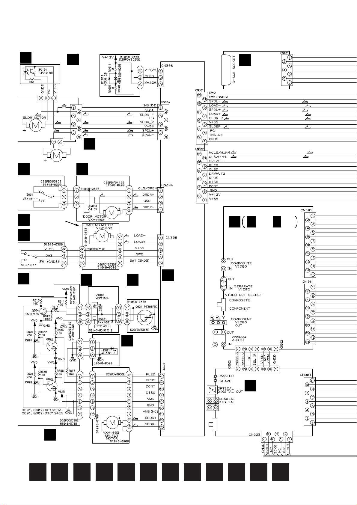
8.14 POWER SUPPLY ASSY
POWER SUPPLY ASSY (VWR1317)
V
R110
T101
TRANS
D201
R101
C102
C104 C103
L101
C101
Z101
D102 D101
D103 D104
C105
C106
PC102
C109
R121
C123
R130
R113
Q103
R114
D110
Q102
R109
PC101
R102
R103
R112
R122
R123
D109
R104
D105
D106
C111
L102
D108
D107
C108
C107
C110
R107 R106
R115
Q101
T102
TRANS
D202
D203
D204
D206
D205
L207 P202
D301
R206
10
C204
3300/10
C205
100/35
REK1078
2A/125V
CN101
AC IN
V
F101
GND
Q121
R124
Q122
C122
C121
R128
PC121
40
R127
D121
R129
R126R125
D302
C301
470/10
Page 43

NOTE OF SPARE PARTS IN POWER SUPPLY (SYPS) ASSY
• In case of repairing, use the described parts only to prevent an accident.
• Please write the red mark on the board when the primary section of POWER SUPPLY (SYPS) Assy is repaired.
• Please take care to keep the space, not touching other parts when replacing the parts.
• NOTE FOR FUSE REPLACEMENT
CAUTION -
C201
1000/16
C202
1000/16
R201
47
PC101
C203
2200/10
IC201
R301
470
R302
PC121
R305
C303
1k
IC301
1k
0.1
FOR CONTINUED PROTECTION AGAINST RISK OF FIRE.
REPLACE WITH SAME TYPE AND RATINGS ONLY.
L201
R205
R303
2.2k
R304
2.7k
0.1/25
1k
R208
5.6k
R209
5.6k
VR301
1k
R202
1k
C213
L301
20µH
R203
3.3k
R204
2.7k
D207
VR201
1k
L205
20µH
20µH
L202
20µH
C302
100/16
C206
100/16
C207
100/16
C210
33/50
IC203
AEK7064
1A
R306
1k
PC102
Q301
C211
100/16
P201
P203
IC202
AEK7066
1.6A
R307
270
R211
R216
1k
100
R215
100
VR202
200
R214
100
C212
100/16
CN201
VKN1202
+M6.0V
1
+M6.0V
2
3
GND
4
GND
5
+12V
6
GND
7
+12V
8
GND
9
GND
10
+5V
11
+5V
12
+5V
13
+3.3V
14
+3.3V
15
+3.3V
16
+3.3V
17
GND
18
GND
19
GND
20
GND
21
GND
22
E+5.0V
23
P. CONT
24
FLAC-A
25
FLAC-B
26
-27V
CN110
1/4
M
41
V
Page 44

WAVEFORMS
Note : The encircled numbers denote measuring point in the schematic diagram.
Measurement condition : No. 1 to 4 and 6 to 11 : Disc MA1, Title 1-chp 1
No. 5 : CD, ABEX-784 Track 1
No. 12 to 14 : MJK1, Title 1-chp 4 or T2-1
No. 15 to 17 : MJK1, Title 1-chp 5 or T2-19
No. 18 to 20 : T2-19, Color-bar (WY and WV Types only)
DVDM ASSY
Foot of R169 (RF)
1
V: 100mV/div. H: 0.2µsec/div.
CN201 - pin 5, 6 (RFO)
2
V: 500mV/div. H: 0.1µsec/div.
IC701 - pin 170 (MY CHIP input)
3
V: 1V/div. H: 0.2µsec/div.
GND
GND
GND
Q281 - Collector (FG)
7
V: 1V/div. H: 5msec/div.
Foot of R261 (FPWM)
8
V: 1V/div. H: 5msec/div.
Foot of R262 (VPWM)
9
V: 1V/div. H: 5msec/div.
GND
GND
GND
VQEB ASSY
Q541 Base (Composite Video output)
1
V: 0.1V/div. H: 10µsec/div.
Q551 Base (Y output)
2
V: 0.1V/div. H: 10µsec/div.
Q531 Base (C output )
3
V: 0.1V/div. H: 10µsec/div.
GND
GND
GND
CN201 - pin 9, 10 (Tracking Error)
4
(AI-Inner Tracking Off)
V: 500mV/div. H: 2msec/div.
IC201 - pin 39 (EFM before slice)
5
V: 1V/div. H: 1µsec/div.
IC201 - pin 1 (EFM)
6
V: 1V/div. H: 0.2µsec/div.
GND
GND
Foot of R263 (PPWM)
10
V: 1V/div. H: 5msec/div.
Foot of R264 (RPWM)
11
V: 1V/div. H: 5msec/div.
GND
GND
B
Q541 Base (C
4
color difference output)
V: 0.1V/div. H: 10µsec/div.
Q551 Base (Y output when selecting
5
color difference output)
V: 0.1V/div. H: 10µsec/div.
Q531 Base (CR output when selecting
6
color difference output)
V: 0.1V/div. H: 10µsec/div.
output when selecting
GND
GND
42
Page 45

NOTE FOR PCB DIAGRAMS :
1. Part numbers in PCB diagrams match those in the schematic
diagrams.
2. A comparison between the main parts of PCB and schematic
diagrams is shown below.
3. The parts mounted on this PCB include all necessary parts for
several destinations.
For further information for respective destinations, be sure to
check with the schematic diagram.
4. View point of PCB diagrams.
Symbol In PCB
Diagrams
Symbol In Schematic
Diagrams
Part Name
BCE
D
DGGSS
BCE
BCE
DGS
BCEBCE
BCE
Transistor
Transistor
with resistor
Field effect
transistor
Resistor array
3-terminal
regulator
Capacitor
Connector
P.C.Board
Chip Part
SIDE A
SIDE B
9. PCB CONNECTION DIAGRAM
43
Page 46

9.1FGSB, SMEB, SSRB, SEMB, LOMB, LOSB, RADB, PHOB,DOMB, DOSB,
VOLB and LEDB ASSYS
FGSB ASSY
A
PC101
R101
SSRB ASSY
C
VOLB
K
ASSY
VR601
Q603
Q601Q602
(VNP1778-A)
Q604
(VNP1661-B)
Q621
(VNP1727-B)
PHOB
H
ASSY
(VNP1727-B)
SMEB
B
ASSY
D
Q
CN306
CARRIAGE
SEMB
ASSY
M
MOTOR
Q
CN303
Q
CN307
(VNP1695-A)
SELECT MOTOR
(VNP1727-B)
G
(VNP1727-B)
L
M
SPINDLE
MOTOR
M
RADB
ASSY
LEDB
ASSY
DOMB ASSY
I
Q
CN304
LOMB ASSY
E
Q
CN305
SIDE A
LOADING
MOTOR
M
(VNP1727-A)
LOSB ASSY
F
(VNP1727-B)
M
DOOR
MOTOR
(VNP1778-A)
DOSB
J
ASSY
(VNP1778-A)
A B C D E F G H I J K L
(VNP1778-A)
44
Page 47

SEMB ASSY
D
(VNP1727-B)
RADB
G
ASSY
LEDB
L
ASSY
(VNP1727-B)
H
PHOB
ASSY
SSRB ASSY
C
(VNP1727-B)
(VNP1727-B)
VOLB ASSY
K
(VNP1778-A)
(VNP1778-A)
LOSB ASSY
F
(VNP1727-B)
DOMB ASSY
I
LOMB ASSY
E
DOSB
J
ASSY
(VNP1727-B)
SIDE B
(VNP1778-A)
(VNP1778-A)
C D E F G H I J K L
45
Page 48

9.2 DVDM ASSY
• This PCB is a four-layered board.
PICKUP
ASSY
DVDM ASSY
M
O
CN101
O
CN501
CN401
R
VR851
VC21
IC23
IC26
IC31
Q810 Q808
IC25
IC54
Q809 Q807 Q811
IC21
IC801
IC807
IC22
IC903
IC261
IC302
Q812
IC806
IC303
IC702
Q
CN301
CN201
V
CN701
S
CN901
P
(VNP1706-B)
Q
Q112
IC101 IC601
Q102
Q281
IC352 IC603
CN302
IC610
Q111
Q107
IC761
IC606
Q601
Q602
M
SIDE A
46
Page 49

N
CN101
DVDM ASSY
M
• This PCB is a four-layered board.
IC905
IC803
IC27
IC805
IC802
IC73
IC201
IC701
Q542
IC608
Q106
IC299
Q543
IC904
IC609
IC611
IC612
IC751
IC792
IC604
IC607
IC231
Q179
Q105 Q237
Q113
Q114
Q101
Q103
IC791
Q106
Q251
SIDE B
47
(VNP1706-B)
M
Page 50

9.3 AVJB ASSY
AVJB ASSY
O
Q120
IC203
IC206
IC202
IC201
IC241
IC150
Q150
Q588
IC501
IC502
Q589
Q592
Q591
Q586
Q587
Q590
O
M
CN901
CN905
M
SIDE A
48
P
(VNP1725-B)
CN902
Page 51

AVJB ASSY
O
Q201
Q257
Q277
Q281
Q151
Q202
(VNP1725-B)
Q582
Q584
Q561
Q583
Q581
Q585
SIDE B
49
O
Page 52

9.4 VQEB ASSY
VQEB ASSY
N
SIDE A
SIDE B
VQEB ASSY
N
VR102
VR101
Q551 Q541
Q531
Q521 Q511
Q501
IC103
(VNP1696-B)
IC106IC1
IC105
N
M
Q1
CN802
Q502 Q512
Q522 IC104
Q532 Q542
Q552
(VNP1696-B)
IC102
50
Page 53

9.5 MSJB ASSY
MSJB ASSY
P
(VNP1778-A)
S
M
O
CN702
CN903
CN502
MSJB ASSY
P
IC921 IC922 IC931 IC901
Q990
Q989
SIDE A
(VNP1778-A)
SIDE B
51
P
Page 54

9.6 MDRB ASSY
MDRB ASSY
Q
I
J631
E
J651
L
J1601
M
CN921
M
CN1030
MDRB ASSY
Q
Q301
Q302
IC301
Q
VR301
Q303
B
CN202
D
J601
(VNP1778-A)
SIDE A SIDE B
52
Page 55

9.7 232B ASSY (DV-F07 ONLY)
232B ASSY
R
M
CN106
IC401
232B ASSY
R
(VNP1778-A)
SIDE A
SIDE B
53
(VNP1778-A)
R
Page 56

9.8 FLKY, KEYB and PS2B ASSYS
FLKY ASSY
S
P
CN903
M
CN602
S
IC701
IC702
SIDE A
54
(VNP1778-A)
Page 57

IC1251
IC1201
KEYB ASSY
T
U
(VNP1778-A)
PS2B
ASSY
(VNP1778-A)
UT
55
Page 58

KEYB ASSY
T
(VNP1778-A)
UT
56
(VNP1778-A)
U
PS2B
ASSY
Page 59

FLKY ASSY
S
SIDE B
57
(VNP1778-A)
Q701Q702
S
Page 60

9.9 POWER SUPPLY ASSY
POWER SUPPLY ASSY
V
AC IN
Q103
Q102
Q101
Q122
Q121
M
CN110
SIDE A
VR201
VR301
VR202
IC201
IC203 IC202
IC301
Q301
V
58
Page 61

10. PCB PARTS LIST
NOTES:•Parts marked by "NSP" are generally unavailable because they are not in our Master Spare Parts List.
The mark found on some component parts indicates the importance of the safety factor of the part.
•
Therefore, when replacing, be sure to use parts of identical designation.
When ordering resistors, first convert resistance values into code form as shown in the following examples.
•
Ex.1 When there are 2 effective digits (any digit apart from 0), such as 560 ohm and 47k ohm (tolerance is shown by J=5%,
and K=10%).
560 Ω→56 × 10
47k Ω→47 × 10
0.5 Ω→R50 ..................................................................................... RN2H
1 Ω→1R0 ..................................................................................... RS1P 1 R 0 K
Ex.2 When there are 3 effective digits (such as in high precision metal film resistors).
5.62k Ω→ 562 × 10
1
→ 561 ........................................................RD1/4PU 5 6 1 J
3
→ 473 ........................................................RD1/4PU 4 7 3 J
R 5 0
1
→ 5621 ...................................................... RN1/4PC 5 6 2 1 F
K
A
FGSB ASSY
Mark No. Description Part No.
SEMICONDUCTOR
PC101 TLP910(O) *HW100480R
RESISTORS
NSP All Resistors RS1/10SxxxJ —
B
SMEB ASSY
Mark No. Description Part No.
SWITCH
S201 DSG1016 *SP001020R
OTHERS
NSP CN201 52044-0345,
3P FFC CONNECTOR —
NSP CN202 VKN1212, 8P
FFC CONNECTOR —
NSP —
C
SSRB ASSY
Mark No. Description Part No.
Q604 2SC1740S HT317402F0
Q601,Q602 DTC124ES BA20003000
D601,D602 GP1S58V HW10036320
NSP All Resistors RD1/4PUxxxJ —
VNP1695, PC BOARD SMEB
SEMICONDUCTORS
RESISTORS
—
E
LOMB ASSY
Mark No. Description Part No.
OTHERS
NSP —
NSP —
NSP J652
NSP J651
F
LOSB ASSY
Mark No. Description Part No.
— VSK1011, LEAF SWITCH *SM000340R
NSP —
G
RADB ASSY
Mark No. Description Part No.
D611 GL381J *HI100870R
NSP —
NSP — RNK1795, LED HOLDER —
H
PHOB ASSY
Mark No. Description Part No.
Q621 PT381FBC *HF000050R
51048-0300, 3P CABLE HOLDER
51048-0500, 5P CABLE HOLDER
D20PDD0310E, JUMPER WIRE 3P
D20PDY0530E, JUMPER WIRE 5P
SWITCH
OTHERS
51048-0300, 3P CABLE HOLDER
SEMICONDUCTOR
OTHERS
51048-0300, 3P CABLE HOLDER
SEMICONDUCTOR
—
—
—
—
—
—
OTHERS
NSP —
NSP —
NSP J603
NSP J602
NSP J605
D
SEMB ASSY
Mark No. Description Part No.
NSP —
NSP —
NSP J601
51048-0300, 3P CABLE HOLDER
51048-0700, 7P CABLE HOLDER
D20PDD0310E, JUMPER WIRE 3P
D20PDD0725E, JUMPER WIRE 7P
D20PDY0310E, JUMPER WIRE 3P
OTHERS
51048-0700, 7P CABLE HOLDER
51048-0900, 9P CABLE HOLDER
D20PDY0930E, JUMPER WIRE 9P
—
—
—
—
—
—
—
—
OTHERS
NSP —
NSP J604
I
DOMB ASSY
Mark No. Description Part No.
NSP All Resistors RS1/10SxxxJ —
NSP —
NSP —
NSP J631
59
51048-0300, 3P CABLE HOLDER
D20PDY0315E, JUMPER WIRE 3P
RESISTORS
OTHERS
51048-0300, 3P CABLE HOLDER
51048-0400, 4P CABLE HOLDER
D20PDY0445E, JUMPER WIRE 4P
—
—
—
—
—
Page 62

J
DOSB ASSY
Mark No. Description Part No.
SWITCH
S631 VSK1011, LEAF SWITCH *SM000340R
OTHERS
NSP —
NSP J632
K
VOLB ASSY
Mark No. Description Part No.
VR601 VCP1158 (22kW) *RA000970R
NSP CN604,CN605 52147-0310, 3P
NSP KN601
L
LEDB ASSY
Mark No. Description Part No.
D1611 HZU6.2B *HZ300030R
D1601 NSPB500-9235 *HI100880R
NSP All Resistors RS1/10SxxxJ —
NSP — 51048-0300, 3P
NSP J1601 D20PDY0325E,
M
DVDM ASSY
Mark No. Description Part No.
IC21 CY2081SL-655 *HC105840R
IC101 LA9701M *HC105850R
IC201 LC78652W *HC105860R
IC609 LC89170M HC10390030
IC352 M56788FP *HC105870R
IC801 M65773AFP *HC105880R
IC802 MB811171622A-100FN *HC105890R
IC803 M5M4V18165DTP-6S *HC106040R
IC612,IC904 MC74VHC541DT *HC700230R
IC608,IC611,
IC807,IC905 MC74VHCT541ADT *HC700240R
IC607 MC74VHCT574ADT *HC700250R
IC702 MN414800CSJ-07 *HC105900R
IC261,IC302 NJM2100M HC10085090
IC601 PD3410A *HU100400R
IC701 PD4995A *HU100410R
IC604 TC55V1001AF8 *HC105910R
IC606 TC7SET32F *HC105920R
IC751 TC7SH32FU *HC105930R
IC24-IC27,IC303
IC610 TC7W53FU HC007105K0
IC22 TC7WH74FU *HC105950R
IC603 VYW1701 *HC105960R
Q106,Q109 2SA1576A HX100012A0
Q105,Q114,Q251
Q602 DTA114EUA *BA000900R
Q107,Q111,Q601
51048-0300, 3P CABLE HOLDER
D20PDD0315E, JUMPER WIRE 3P
RESISTOR
OTHERS
JUMPER CONNECTOR —
PKX1001, JUMPER TERMINAL
SEMICONDUCTORS
RESISTORS
OTHERS
CABLE HOLDER —
JUMPER WIRE 3P —
SEMICONDUCTORS
TC7SHU04F *HC105940R
2SC4081 HX300012A0
DTC114EUA *BA000910R
—
—
—
Mark No. Description Part No.
Q102 HN1A01F BA10011050
Q103,Q281,
Q542,Q543 HN1B04FU *BA000920R
Q101 HN1C01F *BA000930R
Q112,Q113 HN1C01FU *BA000940R
Q108 HN1K03FU *BA000950R
Q503 RN1911 *BA000960R
D302 KV1470 *HZ400010R
D601 RB501V-40 *HZ200100R
D501,D502 RB521S-30 *HZ200110R
COILS AND FILTERS
F5050,F5090 DTF1067, CHIP BEAD *FC900220R
F4010,F4020,
F4030,F4040,
F4050 DTF1070, CHIP BEAD *FC900230R
F4060,F8330,
F9590 DTF1070, CHIP BEAD *FC900230R
NSP L304
L151
L47 VTL1084, CHIP BEAD *FC900240R
L1400 VTL1088, CHIP BEAD *FC900250R
L9490,L9500,
L9510 VTL1105, CHIP BEAD
NSP L101,L330
NSP C612 CCSRCH100D50 —
NSP
C123,C145,C21,
C282,C617 CCSRCH101J50 —
NSP C26 CCSRCH120J50 —
NSP C126,C333 CCSRCH150J50 —
NSP
C206,C210,C211
NSP C322 CCSRCH180J50 —
NSP
C116,C151,C314
NSP C152 CCSRCH221J50 —
NSP C632 CCSRCH330J50 —
NSP C209 CCSRCH331J50 —
NSP
C104-C108,
C128,C134,C297
NSP C335 CCSRCH470J50 —
NSP C122,C208 CCSRCH471J50 —
NSP C127,C334 CCSRCH5R0C50 —
NSP C124,C146 CCSRCH680J50 —
NSP C117,C240,
C352,C360 CCSRCH681J25 —
NSP
C129,C142,
C22,C405,C601
NSP
C701,C763,
C801,C802,C804
NSP
C113,C139,
C358,C368,C411
NSP
C111,C147,
C149,C205,C207
NSP
C401,C403,C407
NSP C502 CKSQYB103K50 —
NSP
C140,C223,
C224,C252,C264
NSP C312 CKSQYB105K10 —
NSP C229 CKSQYB224K16 —
NSP C217 CKSQYF105Z16 —
NSP C216,C313 CKSRYB102K50 —
NSP
C133,C136,
C203,C220,C225
NSP
C239,C320,
C321,C619,C703
NSP C722 CKSRYB103K50 —
VTL1059, CHIP COIL (1.5mH)
VTL1061, CHIP COIL (10mH)
VTL1125, CHIP COIL (8.2mH)
CAPACITORS
CCSRCH151J50 —
CCSRCH220J50 —
CCSRCH470J50 —
CEV101M10 —
CEV101M10 —
CEV220M16 —
CEV470M6R3 —
CEV470M6R3 —
CKSQYB105K10 —
CKSRYB103K50 —
CKSRYB103K50 —
—
*LU000130R
*FC900260R
—
60
Page 63

Mark No. Description Part No.
NSP
C101,C102,
C114,C118,C119
NSP
C121,C130,
C138,C204
NSP
C212,C213,
C227,C228,C231
NSP
C24,C263,
C315-C317,C332
NSP C281,C354 CKSRYB222K50 —
NSP C153,C266 CKSRYB223K25 —
NSP
C214,C251,C261
NSP C357 CKSRYB473K16 —
NSP C330 CKSRYB682K50 —
NSP
C109,C110,
C120,C131,C148
NSP
C150,C202,
C215,C221,C222
NSP
C226,C230,
C235,C265,C29
NSP
C31,C33,
C35,C359,C367
NSP
C369-C372,
C402,C404,C406
NSP C408,C410,
C412,C501 CKSRYF104Z16 —
NSP
C602-C611,
C613-C616,C618
NSP
C621-C631,
C702,C704-C714
NSP C716-C721,
C723-C725 CKSRYF104Z16 —
NSP
C761,C762,
C822,C827,C829
NSP
C832,C833,
C836,C920,C921
NSP
C834,C838,C840
NSP C143,C319,
C806-C819 CKSRYF105Z10 —
NSP
C328,C821,
C824,C825,C828
NSP C830,C837 VCG1030 (2.2mF) —
NSP C23,C299 VCG1032 (0.47mF) —
NSP VC21 VCM1013 (30pF) —
NSP R123 ACN7047 (39W±4) —
NSP R715,R716 ACN7077 (47W±4) —
NSP R531,R543,
R545,R613 DCN1094 (10kW±4) —
NSP
R648,R649,
R706,R707,R748
NSP R751 DCN1094 (10kW±4) —
NSP
R121,R532,
R689,R691,R732
NSP
R736,R785,
R786,R818-R820
NSP
R825,R848,R849
NSP
R1020,R162,
R2010,R2020,R2030
NSP
R2040,R3050,
R3520,R506,R510
NSP
R520,R601,
R701,R801,R8410
NSP R9200,R9210,
R9230,R9240 RS1/10S0R0J —
NSP
R939-R948,
R952-R958,R960
CKSRYB104K16 —
CKSRYB104K16 —
CKSRYB104K16 —
CKSRYB104K16 —
CKSRYB472K50 —
CKSRYF104Z16 —
CKSRYF104Z16 —
CKSRYF104Z16 —
CKSRYF104Z16 —
CKSRYF104Z16 —
CKSRYF104Z16 —
CKSRYF104Z16 —
CKSRYF104Z16 —
CKSRYF104Z16 —
CKSRYF104Z16 —
VCG1030 (2.2mF) —
RESISTORS
DCN1094 (10kW±4) —
DCN1104 (22W±4) —
DCN1104 (22W±4) —
DCN1104 (22W±4) —
RS1/10S0R0J —
RS1/10S0R0J —
RS1/10S0R0J —
RS1/10S0R0J —
Mark No. Description Part No.
NSP
R964,R973-R975,
R979
NSP R361,R364 RS1/16S1203F —
NSP R363,R365 RS1/16S1503F —
NSP R164 RS1/16S5600F —
NSP R3510 VCN1120 (100W) —
NSP Other Resistors RS1/16SxxxJ —
X601
NSP — VDA1681,
NSP CN106 VKN1299,
NSP CN201 VKN1324,
NSP CN120 VKN1464, 24P
NSP CN1030,CN921 VKN1471, 12P
NSP CN905 VKN1473, 14P
NSP CN602,CN901 VKN1474, 15P
NSP CN110 VKN1479, 26P
NSP CN903 VKN1497, 11P
NSP CN802
NSP CN107 VKN1575, 7P
NSP — VRW1773,
X21
N
VQEB ASSY
Mark No. Description Part No.
IC102 MB811171622A-100FN
IC101 PM0023AF
IC105,IC106 TC7SH14FU
Q531,Q532,
Q541,Q542 2PB709A
Q551,Q552 2PB709A
NSP F102 VTF1155, VIDEO FILTER —
NSP L101 VTL1067, CHIP COIL —
NSP C130 CCSRCH102J50 —
NSP C101,C120 CEV101M16 —
NSP
C110-C119,
C121-C126,C150
NSP C160,C532,
C542,C552 CKSRYB104K16 —
NSP C201,C202
(2.2mF) VCG1031 —
NSP R105,R106,
R404,R405 DCN1104 (22W±4) —
RS1/10S0R0J —
OTHERS
DSS1110,
CHIP CERALOCK (20MHz)
FLEXIBLE CABLE 7P —
7P FFC CONNECTOR —
B TO B CONNECTOR 14P
FFC CONNECTOR —
FFC CONNECTOR —
FFC CONNECTOR —
FFC CONNECTOR —
FFC CONNECTOR —
FFC CONNECTOR —
VKN1529,
B TO B CONNECTOR 40P
FFC CONNECTOR —
BARCODE LABEL —
VSS1129, CRYSTAL
RESONATOR (13.824MHz)
SEMICONDUCTORS
COIL AND FILTER
CAPACITORS
CKSRYB104K16 —
RESISTORS
*FQ000450R
—
—
*JX000670R
*HC105890R
*HC105970R
*HC105980R
*HX200080R
*HX200080R
61
Page 64

Mark No. Description Part No. Mark No. Description Part No.
NSP
R12,R201,
R409,R418,R419
NSP R501 RS1/10S0R0J —
NSP R122 RS1/10S2701F —
NSP
R532,R542,R552
NSP
R534,R544,R554
NSP Other Resistors RS1/16SxxxJ —
NSP CN101
O
AVJB ASSY
Mark No. Description Part No.
IC203 BA4560F *HC105990R
IC502 BU4551BF HC10180210
IC501 LA7135AM *HC106000R
IC241 PD0236AM *HC106060R
IC206 NJM78L05A HC38105090
IC150 NJM78M08FA *HC300270R
IC201 PE8001A *HC106050R
IC202 TC7SU04F HC700405Z0
Q202,Q581-Q584
Q151,Q281,Q585
Q150 2SB1260 *HT200240R
Q120 2SC1740S HT317402F0
Q257,Q277 2SD2114K HX421141V0
Q201,Q561,
Q586-Q589 PDTC124EK *BA000970R
D230 HZU5.6B *HZ300040R
D281 MA111 *HZ200120R
NSP L220 DTL1028, CHIP INPEDER —
NSP L202 LAU1R0J-TA —
F201,F241 VTF1096,
S501 VSH1009 *SS000630R
RY281 RSR1029 *LY000240R
NSP C253,C273 CCSQCH221J50 —
NSP C251,C271 CCSQCH330J50 —
NSP C523-C525 CCSQCH470J50 —
NSP C255,C275 CCSQSL331J50 —
NSP
C104,C154,
C211,C232,C501
NSP C526,C528,
C581,C582 CEAT101M10 —
NSP
C102,C121,
C122,C152,C231
NSP C203,C541,
C555,C560 CEAT102M6R3 —
NSP C206,C207 CEAT470M16 —
NSP C250,C252,
C270,C272 CEAT470M25 —
NSP C550,C552 CEAT471M6R3 —
NSP C150 CKSQYB103K50 —
NSP C520-C522,
C561,C585 CKSQYB104K25 —
NSP C587 CKSQYB222K50 —
NSP C583 CKSQYB473K50 —
RS1/10S0R0J —
RS1/16S3300F —
RS1/16S4700F —
OTHERS
B TO B CONNECTOR 40P
SEMICONDUCTORS
2PB709A *HX200080R
2PD601A *HX400120R
COILS AND FILTER
CHIP SOLID INDUCTOR *LU000140R
SWITCH AND RELAY
CAPACITORS
CEAT101M10 —
CEAT101M16 —
—
NSP C
NSP
NSP
NSP C241,C243 CKSQYF104Z25 —
NSP C281,C290,
NSP
NSP
NSP C531 CKSQYF105Z16 —
NSP R597-R599 RN1/10SC18R0D —
NSP
NSP R558,R581,
NSP R250,R270 RN1/10SE1602D —
NSP R251,R271 RN1/10SE2702D —
NSP Other Resistors RS1/10SxxxJ —
NSP CN502 VKN1183, 7P
NSP CN101 VKN1190, 14P
NSP CN501 VKN1191, 15P
NSP —
P
Mark No. Description Part No.
NSP L902 RTF1167, NOISE FILTER —
NSP C932 CCSQCH101J50 —
NSP C902,C912,
NSP C903,C931 CKSQYF103Z50 —
NSP
NSP
101,C103,
C120,C123,C151
C153,C204,
C205,C208,C209
C214,C215,
C230,C233,C234
C502,C527 CKSQYF104Z25 —
C529,C530,C590
C201,C202,
C210,C212,C213
R533,R534,
R542,R551,R555
R585,R589 RN1/10SC62R0D —
CN503 AKP7023, DUAL 4P
JA505 VKB1152, 3P PIN JACK *YT002040R
JA201 VKB1133, 4P PIN JACK *YT002050R
JA504 VKB1135, 2P PIN JACK *YT002060R
CKSQYF104Z25 —
CKSQYF104Z25 —
CKSQYF104Z25 —
CKSQYF104Z25 —
CKSQYF105Z16 —
RESISTORS
RN1/10SC62R0D —
OTHERS
MINI DIN SOCKET *YT002030R
FFC CONNECTOR —
FFC CONNECTOR —
FFC CONNECTOR —
VNE1948, SCREW TERMINAL
—
MSJB ASSY
SEMICONDUCTORS
IC922 TC74HC00AF
IC901,IC931 TC74HCU04AF
Q989 2SA1037K
Q990,Q991 2SC2412K
D989 1SS355 *HZ200130R
COILS AND FILTERS
L901 PTL1003, PULSE TRANS. *TP000040R
F901,F904,
F912,F922 VTF1096,
CHIP SOLID INDUCTOR *LU000140R
SWITCH AND RELAY
S901 VSH1009 *SS000630R
CAPACITORS
C915,C958 CEAT101M10 —
C905,C906,
C913,C916,C922
C933,C936,
C959,C989,C991
CKSQYF104Z25 —
CKSQYF104Z25 —
HC700000Z0
HC700400Z0
HX110373A0
HX324121M0
62
Page 65

Mark No. Description Part No.
Mark No. Description Part No.Mark No. Description Part No.
NSP C990 CEAT470M10 —
RESISTORS
NSP All Resistors RS1/10SxxxJ —
OTHERS
CN904,CN905 AKN1028, MINI JACK *YT002090R
JA902
JA909 VKB1148, 2P PIN JACK *YT002070R
JA989 VKB1149, 2P PIN JACK *YT002080R
NSP CN902,CN903 VKN1267, 7P
NSP CN901 VKN1271, 11P
NSP —
Q
MDRB ASSY
Mark No. Description Part No.
IC301 LA6531 *HC106010R
Q303 2SA1037K
Q301 2SC2412K
Q302 PDTC124EK *BA000970R
NSP C306 CCSQCH101J50 —
NSP C303 CEAT101M10 —
NSP C301 CEAT470M16 —
NSP C302,C304,
C305,C307 CKSQYF104Z25 —
NSP R333 RS1/10S1503F —
NSP R302,R329 RS1/10S1803F —
NSP R311,R312 RS1/10S2202F —
NSP R335,R336 RS1/10S3003F —
NSP R322,R323,
R326,R327 RS1/10S3302F —
NSP R324,R328 RS1/10S3902F —
NSP R334,R338 RS1/10S3903F —
NSP
Other Resistors
NSP CN306 52147-0310, 3P
NSP CN304 52147-0410, 4P
NSP CN305 52147-0510, 5P
NSP CN307 52147-0910, 9P
NSP CN303 VKN1239, 8P
NSP CN301,CN302 VKN1243, 12P
R
232B ASSY
Mark No. Description Part No.
IC401 MAX232EPE
F401-F403 VTH1009, EMI FILTER *FM100080R
GP1F32T, OPTICAL LINK OUT
FFC CONNECTOR —
FFC CONNECTOR —
VNE1948, SCREW TERMINAL
SEMICONDUCTORS
CAPACITORS
RESISTORS
RS1/10SxxxJ —
OTHERS
JUMPER CONNECTOR —
JUMPER CONNECTOR —
JUMPER CONNECTOR —
JUMPER CONNECTOR —
FFC CONNECTOR —
FFC CONNECTOR —
SEMICONDUCTOR
FILTERS
YJ15000090
—
HX110373A0
HX324121M0
*HC106020R
Mark No. Description Part No.
CAPACITORS
NSP C404,C405 CEANP1R0M50 —
NSP C401 CEAT101M10 —
NSP C403 CEAT1R0M50 —
NSP C402 CKSQYF104Z25 —
NSP C406 CEAL1R0M50 —
RESISTORS
NSP All Resistors RS1/10SxxxJ —
OTHERS
JA401
NSP CN401 VKN1238, 7P
S
FLKY ASSY
Mark No. Description Part No.
IC701 PE5184A
IC702 S-806D HC10077530
Q701-Q704 PDTC124EK *BA000970R
D701 SLR-343VC(NP) *HI100890R
L721,L722 VTL1105, CHIP BEAD *FC900260R
SWITCHES
S701-S708 ASG7013 *SP001010R
NSP C710 CEAL100M50 —
NSP
C701,C703,C709
NSP C740-C743,
C751,C753 CKSQYB102K50 —
NSP C707 CKSQYF102Z50 —
NSP
C702,C704-C706,
C708,C714
NSP C711 CKSQYF104Z50 —
NSP R791 RA10T104J —
NSP R792 RA13T104J —
NSP R794 RA4T104J —
NSP R741 RN1/10SE1001D —
NSP Other Resistors RS1/10SxxxJ —
NSP — 51048-1300, 13P
NSP CN703 HLEM1LS-1, 11P
IR701 GP1U28XP,
V701 VAW1052, FL TUBE
NSP CN702 VKN1238, 7P
NSP CN701 VKN1246, 15P
X701 VSS1142, CERAMIC
DKN1111, 15P D-SUB SOCKET
FFC CONNECTOR —
SEMICONDUCTORS
COILS
CAPACITORS
CEAL470M6R3 —
CKSQYF104Z25 —
RESISTORS
OTHERS
CABLE H OLDER —
FFC CONNECTOR —
REMOTE RECEIVER UNIT
FFC CONNECTOR —
FFC CONNECTOR —
RESONATOR (5MHz) *FQ000460R
*YT002100R
*HC106030R
*HW000110R
*HQ300430R
63
Page 66

T
KEYB ASSY
Mark No. Description Part No.
SEMICONDUCTORS
D1201-D1204 DA204K *HZ200140R
SWITCHES
S1201-S1220 ASG7013 *SP001010R
S1200 PSX1002 *SR000140R
CAPACITORS
NSP C1252 CEAL470M6R3 —
NSP C1201,C1202 CKSQYF103Z50 —
NSP C1203,C1251 CKSQYF104Z25 —
RESISTORS
NSP All Resistors RS1/10SxxxJ —
OTHERS
NSP CN1202 HLEM1LS-1, 11P
FFC CONNECTOR —
NSP CN1201 VKN1267, 7P
FFC CONNECTOR —
U
PS2B ASSY
Mark No. Description Part No.
FILTERS
F801-F804 VTH1009, EMI FILTER *FM100080R
CAPACITORS
NSP C801-C804 CCSQCH101J50 —
NSP C813,C814 CKSQYF104Z25 —
RESISTORS
NSP All Resistors RS1/10SxxxJ —
OTHERS
JA801
NSP CN801
V
POWER SUPPLY ASSY
Mark No. Description Part No.
IC203 AEK7064 (1A) *HC300280R
IC202 AEK7066 (1.6A) *HC300290R
— VZF1092, VARISTOR *HV000030R
F101 FUSE (2A) *FS000750R
NSP CN201 26P FFC CONNECTOR —
RKN1038, MINI DIN 6P SOCKET
VKN1267, 7P FFC CONNECTOR
SEMICONDUCTORS
OTHERS
*YT002110R
—
64
Page 67

65
Page 68

11. ADJUSTMENT
11.1 ADJUSTMENT ITEMS AND LOCATION
Note : When the Traverse mechanism adjustment is not properly adjusted, jitter, error rate and play ability are defective.
The noise may come out by the case.
Adjustment Points (PCB Part)
DVDM ASSY
CN703
IC21
IC801
Pin 5
1
VC21
2
VR601
KN601
CN120
IC101
IC601
VOLB ASSY
Adjustment Items
CN1030
[Electrical Part]
CN252
CN110
SIDE A
1
2
11.2 JIGS AND MEASURING INSTRUMENTS
CD TEST DISC
PHILIPS SBC429
Digital multi meter
Frequency counter
Display digit ≥ 8-digit
Jig (Peak hold circuit)
Master Clock Adjustment
Disc-select Rotation Adjustment
A
V
DC power supply
22k
CH1 CH2
(X) (Y)
Oscilloscope
Screwdriver
(small)
Precise screwdriver
Test mode remote
control unit
(GGF1067)
66
INPUT
470
from KN601
(VOLB ASSY)
V+B
0.01
+
33/16
+
M5238(1/2)
–
0.01
33/16
+
SW
V-B
470k
47
0.1 0.1
M5238(2/2)
+
–
CQM or CFTX
OUTPUT
(Peak hold OUT)
Page 69

11.3 NECESSARY ADJUSTMENT POINTS
When
EXCHANGE PCB ASSY
Exchange board
VOLB ASSY, SSRB ASSY,
RADB ASSY, PHOB ASSY
Exchange board
DVDM ASSY
11.4 ELECTRICAL ADJUSTMENT
Mechanical
point
Electric
point
Mechanical
point
Electric
point
Note : is adjusted already.
Adjustment Points
2
1
Master Clock Adjustment
• When not properly adjusted : Uneven color
• Normal mode
• Power ON
Player
START
DVDM ASSY
IC21
DVDM ASSY
33.868800MHz ± 160Hz
VC21
Frequency counter
Pin 5
67
Page 70

2
Disc-select Rotation Adjustment
DC power supply
Connection Diagram for Adjustment
VOLB ASSY
Player
VR601
KN601
JIG
(Peak hold circuit)
SW
INPUT
–8V
GND
+8V
OUTPUT
V
Digital multimeter
GND
(Under Base)
Adjustment Procedure
1. Connect all equipment as shown in the diagram.
2. Turn on the power (Normal mode) and put the test disc in the No. 1 disc slot.
3. Enter the Test mode by pressing the "ESC" → "TEST" button of the test mode remote control unit.
4. Press the "DIG/ANA" button of the test mode remote control unit. (Disc 1 is clamped.)
5. Adjust VR601 on the VOLB Assy so that the voltage becomes 830 ± 5mV.
6. Switch the connection of Digital multimeter from INPUT to OUTPUT of the Jig.
7. Press the "DIG/ANA" button of the test mode remote control unit. (Starts the disc detection and peak hold .)
8. Confirm the voltage during the disc detection.
If voltage is between 920 to 1170mV, go to step 13. If not, go to step 9.
9. Switch the connection of Digital multimeter form OUTPUT to INPUT of the Jig.
10. Press the "DIG/ANA" button of the test mode remote control unit. (Disc 1 is clamped.)
11. Adjust VR601 to become the value for addition (or subtraction) that to have an adjustment voltage.
(Refer to the following table.)
12. Perform steps 6 to 8 again and confirm the voltage during the disc detection.
If voltage is between 920 to 1170mV, go to step 13. If not, repeat steps 9 to 12.
13. Confirm that Disc No. display doesn't become "1" others when you turn the Jog dial.
14. Release the Test mode by pressing the "ESC" button or turn off the power.
A
Adjustment voltage value
Peak hold voltage (mV)
to 859
859 to 879
879 to 920
920 to 1170
1170 to 1309
1309 to 1520
1520 to 1840
1840 to 2220
2220 to
Adjustment voltage (mV)
+20
+10
+ 5
OK
- 5
-10
-20
-30
-40
68
Page 71

Simple Adjustment of Disc Detection
Connection Diagram for Adjustment
Player
VOLB ASSY
VR601
KN601
GND
Stopped
CH2 = 200mV
DC P*10
Go arround
(except for single loader)
CH1 CH2
22 - NOV - 1999 16 46
(X) (Y)
2 s/d
Oscilloscope
Chassis GND
Peak value is
OK with 950 - 1100mV.
Peak
Minimum
Peak
Maximum
VR601
Adjustment Procedure
1. Connect an oscilloscope.
2. Turn the POWER SW to ON.
3. Open the Food.
4. Press the "SINGLE LOADER PLAY" button of the player without putting a disc.
Start the disc detection if loading is come and there is no disc.
5. If the peak value is 950 - 1100mV while a disc detection goes arround the disc, is OK.
6. When peak value is except for OK range, adjust VR601 and repeat steps 3 - 5.
69
Page 72

12. GENERAL INFORMATION
12.1 DIAGNOSIS
12.1.1 TEST MODE SCREEN DISPLAY
Consecutive double-OSD display is supported during test mode. The screen is composed 10 lines with a maximum of 32 characters per line.
It can't be used with the debugging display mode together.
• Screen Composition
Character in bold : Item name
: Information display
Address
Background color
Tracking status
Spindle status and AFB status
AGC setting
FTS servo IC information
C1 error value of CD and DVD
Internal operation mode of
the mechanism control
Disc judgment and
CD 1/3 beam switch
Equalizer value and
jitter value
First Screen Display
Caution :
The first screen and second screen switch by pressing [DISPLAY]
key of the remote control unit.
It is only a version display part on the lower right of the screen
those contents of display change.
ATB : ON/OFF information display and AGC manual setting display
deleted with the second generation.
The displays of Tilt error value, Tilt servo status and pickup
DVD/CLD display deleted with the third generation becomes LD
part is deleted.
Remote control code
Key code
Mechanism position value and
slider position
Output video system and
Skirt terminal output
AV1 chip version
FL controller version and
region setting for the player
FL controller destination setting
Port No. of Flash ROM and
system controller
Flash ROM version and Flash ROM size
System controller revision
DVD mechanism controller revision
(Control and part No. of GUI-ROM)
• Description of Each Item on the Display
(1) Address indication
The address being traced is displayed in number.
DVD : ID indication (hexadecimal number, 8 digits)
[ ∗ ∗ ∗ ∗ ∗ ∗ ∗ ∗ ]
CD : A-TIME (min. sec.) [ 0 0 0 0 ∗ ∗ ∗ ∗ ]
(Note : For DVDs, decimal-number indication is possible.)
(2) Code indication of the remote control unit
[R – ∗ ∗ ∗ ∗]
The code for the key pressed on the remote control unit, which is
received by the FL controller, is displayed while the key is pressed.
In the case of the double code, the second code will be displayed.
(3) Key code indication for the main unit [K – ∗ ∗ ]
The code for the key pressed on the main unit, which is received by
the system controller, is displayed while the key is pressed.
At keyboard code input
K-KBD ∗∗ ∗∗ :
At mouse code input
K-MS ∗∗ ∗∗
(4) Background color indication [C – R∗ ∗ G∗ ∗ B∗ ∗]
(5) Tracking status [TRKG – ∗∗∗]
Tracking on [ON ]
Tracking off [OFF]
(6) 1 Spindle status [SPDL – ∗ ∗ ∗]
Spindle accelerator and brake, free-runnimg [A/B]
FG servo [FG]
Rough, velocity phase servo [SRV]
Offset addition, rough, velocity phase servo [O_S]
2 AFB status [AFB – ∗ ∗]
ON [ON ]
OFF [OFF]
(7) Mechanism position value [M – ∗]
Position code [1] to [3]
(8) Slider position [S – ∗ ∗ ∗ ∗]
CD TOC area [IN ]
CD active area [CD ]
(9) AGC setting [AGC – ∗ ∗]
AGC on [AGC-ON]
AGC off [AGC-OFF]
70
Page 73

(10) Output video system [V – ∗ ∗ ∗ ∗]
NTSC system [NTSC]
PAL system [PAL ]
Auto-setting [AUTO]
Skirt terminal output [SK – ∗ ∗]
VIDEO [00]
S-VIDEO [01]
RGB [02]
∗ : Display only the model which can do the output setting of skirt
terminal.
(19)The part number of the flash ROM and system
controller [∗ ∗ ∗ ∗ ∗ ∗ / ∗ ∗ ∗ ∗ ∗ ∗ ∗ ]
1 Part number of the flash ROM <Front>
(Example) VYW1536-A = W1536A
(Example) PD6256A9 = 6256A9
2 Part number of the system controller <Rear>
(Example) PD3381T1 = 3381T1
(20) 1 Version of the flash ROM [V : ∗ . ∗ ∗ ∗ ]
2 Flash ROM size [FLSH ∗∗ ]
(11) FTS servo IC information
DSP coefficient indication [KS – [∗ ∗ ∗ ∗] ∗ ∗ ∗ ∗ ]
Displays the address (four digits) of the specified coefficient
and the setting value (four digits) with [TEST] and [9] keys.
(12) Error rate indication
1 C1 error value of CD [ER – C1 ∗ ∗ ∗ ∗ ]
2 C1 error value of DVD [ER – ∗ ∗ ∗ ∗ ∗ ∗ ∗ ∗ ]
(13) Internal operation mode of mechanism controller
[MM – ∗ ∗ : ∗ ∗]
Internal mechanism mode (2 digits) and internal mechanism step (2
digits) of the mechanism controller
(14) 1 Disk sensing [DSC – ∗ ∗ ∗]
The type of discs loaded is displayed.
[DVD], [CD ], [VCD], [ ]
2 CD 1/3 beam switch [BM – ∗ ∗]
(15) 1 Equalizer value [E – ∗ ∗]
2 Jitter value [J – ∗ ∗]
nake the jitter four times, and renew it in every one second.
[4 – ∗ ∗]
CD is effective only in the jitter value.
(21) Revision of the system controller
[S : ∗ . ∗ ∗ ∗ / ∗ . ∗ ∗ ]
1 Revision number of the external ROM part (flash ROM) of the
system controller <Front>
2 Revision of the internal ROM part of the system controller
<Rear>
(22) Revision of the DVD mechanism controller
[M : ∗ . ∗ ∗ ∗ ]
Revision number of the external ROM part (flash ROM) of the DVD
mechanism controller
(23) Control and part numbers of the GUI-ROM
[G : ∗ ∗ ∗ ∗ ]
No GUI model displays as "––– / ––––".
OEM model displays the part number of GUI-ROM [G : ∗ ∗ ∗ ∗]
(16) Version of the AV-1 chip [ AV : ∗ . ∗ / ∗ ∗ ∗ ∗ ]
(17) 1 Version of the FL controller
[FL : ∗ ∗ ∗ ∗]
2 Region setting of the player [REG : ∗ ]
Setting value [1] to [6]
(18) Destination setting of the FL controller
[MDL : ∗ ∗ ∗ ∗ / ∗ ∗ ∗ ]
For charactors in front represent the type of model :
There charactors that follow represent the destination code.
J : /J, K : /KU, /KC, /KU/KC, R : /RAM, /RL, /RD, /LB,
WY : /WY
71
Page 74

12.1.2 TROUBLE SHOOTING
• No Power ON
• FL is not turned ON
• FL indication is unusual
START
Turn on the power again
after 2 - 3 minutes.
Is FL turn on ?
Yes
Is the indication
of FL normal ?
Yes
Power ON
No
No
• Blow out fuse (F101) of the primary side.
• Varister (Z101) on the POWER SUPPLY Assy is damaged.
• Blow out micro-fuse (P201, P202, P203) on the POWER SUPPLY Assy.
(Check the each voltage.)
• FL controller IC (IC701) on the FLKY Assy is damaged.
• Check the following connections :
POWER SUPPLY Assy - DVDM Assy (26P flexible cable)
DVDM Assy - FLKY Assy (15P flexible cable)
FLKY Assy - KEYB Assy (11P flexible cable)
• Check each voltage (EV+5V, SW+5V, SW+3.3V, +6V and +12V)
(If above voltage are not supplied, check the micro-fuse.)
• Short or open the zenner diode
on the POWER SUPPLY Assy.
FL indication is dark or flickers.
Indicates the error message
• Blow out micro-fuse (P201) on the POWER
SUPPLY Assy.
(D207)
• Check the values of R761 - R763
on the FLKY Assy.
Refer to the section "7.1.4 ERROR CODE".
Is door open ?
Yes
Do the video and
sound come on ?
Yes
OK
No
No
• Check the following connections :
DVDM Assy (CN1030) - MDRB Assy (CN301) (12P flexible cable)
DVDM Assy (CN921) - MDRB Assy (CN302) (12P flexible cable)
MDRB Assy - SEMB Assy (9P parallel cord)
MDRB Assy - DOMB Assy (4P parallel cord)
MDRB Assy - LOMB Assy (5P parallel cord)
• Check the +6V power supply voltage (above micro fuse).
• Check the following connections :
MDRB Assy - SMEB Assy (8P flexible cable)
DVDM Assy - AVJB Assy (15P flexible cable)
DVDM Assy - AVJB Assy (14P flexible cable)
AVJB Assy - MSJB Assy (7P flexible cable)
DVDM Assy - VQEB Assy (B to B connector)
Indicate the error message.
Refer to the section "7.1.4 ERROR CODE".
72
Page 75

12.1.3 OPERATION FLOWCHART
From power-on till the end of initialization
(Power ON)
Initialization of memory
Setup of the destination and the type of player
according to the data received from the microprocessor
for the FL display.
Process of closing the hood
Process of rejecting a disc
Changing the target address of the selector to the
address of the player
(Park)
Until start of playback of the specified disc
(Playback of the specified disc)
Changing the target address of the selector to the
address of the player
Placing the disc in the player with a load command
and clamping it
(Playback)
Closing the hood
(Closing the hood)
Finishing closing
the hood
It there a command
for playback ?
No
Detection of existence of discs through the selector
Yes
During closing
(Playback of the specified disc)
(End of the playback)
Detection of existence of discs through the selector
(Park)
73
Page 76

12.1.4 ERROR CODE
yalpsiDLFsesuacelbissoPtinuehtfonoitarepO
REV1VA rellortnocmetsysfomargorpehthtiwhctamatonsipihc1-VA
RREAUPC).lausunusierawdraH(rorresserddaUPC noitarepooN
RREAAMD).lausunusierawdraH(rorresserddaAMD noitarepooN
DIHSALF
PRWHSALFMORhsalfehtfororretcetorpetirW noitarepooN
GISHSALF
MUSHSALF
EZISHSALF).tib-M8ro4esU(MORhsalfehtfororreeziS noitarepooN
LAGLLI
EVRESER).lausunusierawdraH(tpurretnidenifednU noitarepooN
TOLS ).lausunusierawdraH(deussidnammoctolsetairporppanI noitarepooN
).desu
).lausunusierawdraH(
).lausunusierawdraH(
)rorrerellortnocmsinahceM(
LF
11tuoemithcraeS
21
91
B1
22
32
33
83
rorre
elihw
rorre
AVLC
noitpircseD
rorrEfo
.sdnoces
yrterhcraeS
tuoemitgnicarT
gnigrevnoc
hcraes0xednI
fotuoemiT
renniredils
ecnerefmucric
fotuoemiT
retuoredils
ecnerefmucric
eslupKOFoN
kcabyalpgnirud
-isnes-epyt-csiD
rorregn
.epytcsideht
DVDahtiwfisesuaCDCahtiwfisesuaCtinUehtfonoitarepO
6(tuoemitfoesacaniro,semit
noitallatsniesreverroeruliafenilsubro,MOR
edocnoitareponanahtrehtoedocadehctefrellortnocmetsysehT
7nihtiwetelpmocebtondluochcraeS
.nacs
3retfadetelpmocebtondluochcraesA
4detucexesawpukcabhcraes,seirter
11gnicartsawtinuehtelihw)sdnoces
elihwtegratehtdnoyeberomroskcart
.gnigrevnocsawnoitarepohcraeseht
tagnicartelihw)sdnoces5.01(tuoemiT
.hcraesafoecnegrevnocfoegatseht
.tniopni
.detelpmocsaw
.sdnoces3nihtiwNOtondluochctiwsedisnI potS
.sdnoces2nihtiwFFOtondluochctiwsedisnI potS
.semit02ylsuounitnocdetaivedsawsucofehtnehW
ehtretnetondluoctidna,sdnoces
02(sdnoces3nihtiwdetelpmoceb
tinulortnocetomerehtgnisutuohtiwyalpsidLFehtnodeyalpsideratahtsedocrorrE
.oiduacificepseht
hsalfehtfodnarellortnocmetsysehtfoMORlanretniehtfosnoisrevniecnereffiD
sawdesuebt'dluochcihwMORehtnehW(MORhsalfehtforebmuntrapniecnereffiD
noitallatsniesreverro).ezisralugerehtsdeecxetI(MORhsalfehtfororremuskcehC
noitarepooN
noitarepooN
noitarepooN
noitarepooN
htiwtuotonyamdnuosehT
tinulortnocetomerehtgnisuybyalpsidLFehtnodeyalpsideratahtsedocrorrE
yalpsidLFehtforetnecfostigidowtehttA:yalpsidehtfonoitacoL;YALPSID+YALPSID+CSE:yalpsidoT
neercsVT:yalpsidehtfonoitacoL;tohsenO+YALPSID+CSE:yrotsihrorreehtyalpsidoT
7nihtiwetelpmocebtondluochcraeS
DCVybsdnoces7nihtiwaerategrat
detucexesawpiksredilstsniagapukcaB
piksredilsro,hcraesagnirudsemit4
-daerehtmorfgnitratsnidetlusereciwt
hcraeseht,hcraeS)xednI(kcarTgniruD
tondluocmargorpafogninnigebehtrof
)hcraeSxednIfoesacehtnisdnoces
atadCOTehtnodesabgninoitisopretfa
lliwgnisnesepyt-csid,sesaceerhtgniwollofehtnielbissopmisawgnitratslamronfI
rorresucofehtnehw,revewoH.rorre5Cgnitpecxeeruccosrorrerehtofideirtereb
:tnemomehtta"rorre83"sadehsinifsiti,semit3ylsuounitnocderuccosaw"33"
csidrehtonahtiwputratsdecrof)2(,tlusergnisnes-epyt-csidtsrifehthtiwputrats)1(
gnitangisedybcsidlanigiroehthtiwputratsdecrof)3(,epytcsidehtgnitangisedyb
,spotS:DC
noitareposeunitnoC:DVD
,spotS:DC
noitareposeunitnoC:DVD
potS
potS
tsomrenniehttasucofstsujdA
otseirtdnaecnerefmucric
ehterehwnoitisopstiotnruter
3rof(detarenegsawrorre
.sneponeht,)semit
retfastsisreprorreemasehtfI
oN(.snepoyarteht,yrtereno
)eslupKOF
nepO
74
Page 77

LF
93
14tuoemiteldnipS .dnammocpotSafoecnaussifosdnoces01nihtiwedompotSretnetondidtinuehT potS
84
94
A4tuoemitkcoleldnipS .BFAehttratserofebsdnoces5.1nahteromkcoltondluoceldnipS
15
25
35
45
55
65
75
85
95
A5
B5
C5
D5
F5
26rorreyrteresuaP
tuoemit
GFeldnipS
noitceted
nwodpmuj
pupmuj
gnisnes
NOovres
fotuoemit
saibsucof
fonoitpircseD
rorrE
egrevnocCGS
.kcikeldnips
tuoemitnoitisnart
LLPeldnipS
tuoemitnoitisnart
ecneuqesotuA
kaepfotuoemit
ecneuqesotuA
sucoffotuoemit
ecneuqesotuA
sucoffotuoemit
ecneuqesotuA
CGAyalpfotuoemit
ecneuqesotuA
-epyt-csidfotuoemit
ecneuqesotuA
2BTAfotuoemit
ecneuqesotuA
gnikcartfotuoemit
ecneuqesotuA
1BTAfotuoemit
ecneuqesotuA
sucoffotuoemit
tnemtsujdaniag
ecneuqesotuA
gnikcartfotuoemit
tnemtsujdaniag
ecneuqesotuA
tesffofotuoemit
tnemtsujda
ecneuqesotuA
rotcafnoitaludom
tnemerusaem
ecneuqesotuA
otuafotuoemit
ecneuqesotuA
ysubydaerla
.sdnocesevifnihtiwnoitator
.sdnocesevifnihtiwnoitator
.tnessawdnammoc)BTA
.tnessawdnammoc
.desaelerneebdahtiretfa
DVDahtiwfisesuaCDCahtiwfisesuaC
kaepehtstcetedgnirudegrevnoctondluocCGS nepO
nihtiwotniegrevnoctondluoceldnipsehT ± fo%21
csidretfaemittsrifeht(putratsretfaemittsrifehT
lamronbaehtstceted,putratsretfaemittsrifehT
Sm06ot04:DC,Sm9ot5:DVD
Sm06ot04:DC,Sm9ot5:DVD
ehtretfadnoces1nihtiwnrutertondidYSUBA
.tnessawdnammoc)noitcetedkaep(TCTDD
.tnessawdnammoc)0ot1pmujsucoF(
.tnessawdnammoc)1ot0pmujsucoF(
ehtretfaSm05nihtiwnrutertondidYSUBA
ehtretfasdnoces2nihtiwnrutertondidYSUBA
.tnessawdnammoc)gnisnes-csid(TRSJD
ehtretfadnoces1nihtiwnrutertondidYSUBA
.tnessawdnammoc)NOovresgnikcart(
.tnessawdnammoc)BTAlanretxe(
.tnessawdnammoc)saibsucofotua(
LBTehtretfaSm002nihtiwnrutertondidYSUBA
.tnessawdnammoc)tnemtsujdaniagsucof(
NGTretfasdnoces2nihtiwnrutertondidYSUBA
.tnessawdnammoc)tnemtsujdaniaggnikcart(
ehtretfadnoces1nihtiwnrutertondidYSUBA
.tnessawdnammoc)tnemtsujdatesffo(EVADMC
retfasdnoces01nihtiwdeepsnoitatorGFtegrateht
tegratehtforebmunehtemocebt'nseodti,)noitcnitsid
.spool3ylsuounitnocdeeps-hgihforebmunnoitator
tegratehtforebmunehtemocebt'nseodti,putratsretfasemitdnocesehtretfA
.snoitatordeeps-wolrodeeps-hgihlamronbaehtstceteD
DPMJFehtretfaSm03nihtiwnrutertondidYSUBA
UPMJFehtretfaSm03nihtiwnrutertondidYSUBA
.tnessawdnammoc)gnirusaem-CGA-yalp(NOMUSG
lanretxefonoitelpmocehtretfaBTAlanretnI(SFOLBT
NOSTehtretfaSm005nihtiwnrutertondidYSUBA
NGFehtretfasdnoces2nihtiwnrutertondidYSUBA
RIMJDAehtretfaSm002nihtiwnrutertondidYSUBA
.tnessawdnammoc)tnemerusaemrotcafnoitaludom(
BFAehtretfasdnoces2nihtiwnrutertondidYSUBA
sawYSUBAesuacebtnesebtondluocdnammocA
VLTretfaSm002nihtiwnrutertondidYSUBA.wol
seirtereerhtnihtiwderotserebtondluocedomesuaP
ehtfonoitarepO
tinU
)tuoemitGF(.spotS
.spotS
.spotS
potS
potS
potS
potS
potS
potS
potS
potS
potS
potS
potS
potS
potS
potS
gniruddeyalpsidsi"37"(
).ssecorpgnitrats
gniruddeyalpsidsi"37"(
).ssecorpgnitrats
noitareposeunitnoC
75
Page 78

LF
17
27
37
47
18
28
1A
2A
3A
4A
1B
2B
3BecartrofrorreyrteR
3C
)5C(
3E
5FdehsupgniebyarT
8FtuoemitgnidaoL
CFsucoF
fonoitpircseD
rorrE
daertonnacDI
gnicartgnirud
kcehcedocbuS
gniruderuliaf
kcabyalp
tadaertonnacDI
putratseht
kcehcedocbuS
putratsgniruderuliaf
foCOT
rellortnoc
rellortnoc
dnammoc
pukcab
pukcab
gnidaerroftuoemiT
msinahcemeht
gnidaerroftuoemiT
metsysehtfoCOT
noitacinummoC
PSDfotuoemit
002 µ .)S
noitacinummoC
gnidaerroftuoemit
tneiciffeocPSD
noitacinummoC
gnitirwroftuoemit
tneiciffeocPSD
noitacinummoC
roftuoemit
gnitirwylsuounitnoc
tneiciffeocPSD
rofrorretuoemiT
rofrorreyrteR
tnerrucrevo
tsettiucric-trohS
tsniaganoitaloiV
draugypoclatigid
.PSD
µ ro,gnitirwtneiciffeocsuounitnocgnirudS
gnikcartfonoitceteD
rorregnidnopserroc
.ylsuounitnoc
.ylsuounitnoc
.)sdnoces5
002tuoba(emitdeificeps µ aretfadnaerofeb)S
.PSDotdeussisaw
.eromrodnoces
.yawanurgnitceted
.ecroflanretxenaybnepO
DVDahtiwfisesuaCDCahtiwfisesuaCtinUehtfonoitarepO
.eromrodnoces1rofdaerebtondluocDInA potS
3rofdaerebdluocemarfoN
.eromrosdnoces
retfadnoces1nihtiwdaerebtondluocDInA
.dehsinifneebdahtnemtsujdaBFAeht
.dehsinifneeb
.erom
metsysehtfoCOTgnidaeR
PSDotdeussiebtondluocdnammocA
nisaw)YSUBCX(ysuBdnammoCesuaceb
tuoba(emitdeificepsarof)L=YSUBCX(ecrof
arofecrofnisaw)YSUBCX(ysuBdnammoC
ro,PSDotdeussisawdnammocdaertneiciffeoc
ecnaussidnammocretfakcab-ohcesserddaeht
.sserddaputesehthctamtondid
arofecrofnisaw)YSUBCX(ysuBdnammoC
retfadnaerofeb)Sm4201tuoba(emitdeificeps
otdeussisawdnammocetirwtneiciffeoceht
002rofecrofnisaw)YSUBCX(ysuBdnammoC
dnammocetirwsuounitnocaretfadnaerofeb
1rofdaerebtondluocsedoc,ecneuqespukcabehtgnirudetatsgnicartehtnI
ebtondluocPSDovresehtfoecneuqesNOgnikcart,ecneuqespukcabehtnI
.deussisawdnammocNOgnikcartehtretfaSm005nahteromfinevedetelpmoc
eromrosm003rofLtasawtropnoitcetedtnerrucrevoeht,kcabyalpgniruD
eromrosm04rofLtasawtropnoitcetedtnerrucrevoeht,nosawrewopehtelihW
.semitthgiederuccororregniwollofehT
.tnessaw)PSDovresehtot(dnammocNOsucofeht
.detelpmoctonsawNIsucofyllautca,dehsinifsawecneuqesNIsucoF)2(
3nihtiwdaerebdluocedocbusoN
dahtnemtsujdaBFAretfasdnoces
rosdnoces03koottuodaerCOT
.ecneuqespukcabehtnisemit3rofNOgnikcartehtgnirterretfaelbissopmignicarT spotS
rofsnoitarepopukcabfosnoitaretieerhtretfadetcetedsawyawanur,gnicartgniruD
nahtrehtoedomaotdegnahcylbicrofsawedomnepOneebdahtahthctiwsyartehT
retfasdnocesowtnahteromfinevedetelpmocebtondluocecneuqesNOsucoF)1(
potS
snepO
.)eruliaf
potS
potS
.eromrosdnoces03kootrellortnoc
spotS
spotS
spotS
sesolC
tuoba(emitdeificepsanihtiwdetelpmocebtondluocgnipmalcrognidaolnu,gnidaoL
.spotstinu
)eruliaftuodaerDI(
tuodaeredocbuS(snepO
noitarepooN
noitarepooN
noitarepooN
noitarepooN
lacinahcemeht(spotS
setareporellortnoc
.)yltnednepedni
rewopehtffosnruT
nonoitacidnioN(yltnatsni
ondnayalpsidLFeht
)yromemhsalfotgnitirw
gnidaolehtsesreveR
situoemittI.noitcerid
eht,yrternopudetaeper
elbissopreverehwspotS
ehtnispots(sneponeht
.)Bedisfoesac
E00, E04-E06, E11, E16, E17, E90-E92, E99
: Refer to page 76.
76
Page 79

)rorreeciveD(
LFrorrEfonoitpircseDDVDahtiwfisesuaCDCahtiwfisesuaCtinUehtfonoitarepO
.cte801=3tib
.cte101=1tibrorresseccaMARS
rorressecca1VA
)GNetirw,daer(
tinulortnocetomerehtgnisuybyalpsidLFehtnodeyalpsideratahtsedocrorrE
yalpsidLFehtfotfelfostigidowtehttA:yalpsidehtfonoitacoL;YALPSID+YALPSID+CSE:yalpsidoT
gniggubedsemocebtironoitarepooN
.NOotelbasirewopehtfinoitacidni.cte401=2tibrorresseccaPIHCYM
77
Page 80

12.1.5 INTERFACE CONNECTOR
TxD
RxD
GND
RxD
TxD
GND
Computer
This Unit
• Communication control
The protocol system is based on a system in which the computer
gives commands and the player returns statuses. The communication
protocol used conforms to that used by industrial and educational
equipment (changers, drives, LD players for educational use, etc.)
of our company, and supports Communication Mode 7 (CM 7).
CM 7 uses a method of proceeding a program by issuing each
execution command and confirming the execution status with a
request command.
First, the controller sends an execution command, and the player
returns the status of having received the command. Then, the
controller sends a request command, and the player returns the
corresponding status data. The controller repeats this operation until
it receives the status data required.
In CM 7, neither Completion of Execution Status nor error messages
are returned. Statuses returned in response to execution commands
are the End of Receive message <R> and Communication Errors
<E 00>. To confirm Completion of Execution or occurrence of
errors, use the request command “?J.” However, note that some
commands have restrictions or conditions, and that some commands
cannot be executed or may not be executed as they should be.
• Format
Serial control interface in conformance with the RS-232C Standards
• Connector
15-pin, D-sub connector
9151413121110
1234567
8
• Specifications of Interface
Signal level : RS-232C level
Data format
Data length : 8 bits
Stop bit : 1 bit
Parity : none
Transmission speed (baud rate):
Selectable between 9600 and 19200 bps, by exclusive command
of the player. Every time the power is turned on, the baud rate
is reset to 9600 bps.
Connection:
The computer and this unit are connected through three lines, as
shown below:
The player can receive commands any time as long as the power is
on. So, even when the RS-232C port of the computer is used,
connection of any control lines other than TxD and RxD is NOT
necessary.
However, some computers need physical CTS input for operation.
In this case, the DTR output, which always outputs positive electric
potential as long as transmission is possible, can be used. Connect
the DTR output to the CTS input of the computer as shown below:
Example of connection (connection with a DOS/V computer)
This Unit (Player)
D-SUB 15P
TxD (2)
RxD (3)
GND (1)
DTR (4)
Computer (DOS/V)
D-SUB 9P
RxD (2)
TxD (3)
GND (5)
CTS (8)
• Signal Line
No. Name I/O Function
1 GND − Ground
2 TxD O Transmission output
3 RxD I Receiving input
4 DTR O Transmission permission
5 Reserved −
6 Reserved −
7 Reserved −
8 Reserved −
9 Reserved −
10 Reserved −
11 GND − Ground
12 Reserved −
13 Reserved −
14 Reserved −
15 GND − Ground
78
Page 81

• List of Commands
cinomenMemaNdnammoCtnemugrAboJ
PO
LU
OC
SZ
JR
RZ
LP
PK
AP
TS
FS
RS
FN
RN
SN
ES
MT
HC
IT
RT
US
UA
GA
PA
PR
SD
LC
MP
PC
DU
CB
DI
OK
IN
IA
ON
OA
J?
P?
Z?
E?
T?
R?
C?
A?
K?
H?
M?
X?
Argument: Argument of a command. The values in parentheses are those when the slave player(s) is(are) connected, and "0"
NEPO
DAOLNU
ESOLC
TCELESCSID
TCEJER
NRUTERCSID
YALP
YALPKCART1
ESUAP
LLITS
DRAWROFPETS
ESREVERPETS
DRAWROFNACS
ESREVERNACS
POTSNACS
HCRAES
TESEDOMEMIT
TESEDOMRETPAHC
TESEDOMELTIT
TESEDOMKCART
ELTITBUSTCELES
OIDUATCELES
ELGNATCELES
TCEPSATCELES
TESEDOMTAEPER
LORTNOCYALPSID
RAELC
TESEDOMYALP
TESYALPMOTSUC
ETADPUOTUA
EGNAHCETARDUAB
TUPTUODI-CSID
TUPTUOEPYTCSID
TUPNITXETCSID
TUPNITXETTSITRA
TUPTUOTXETCSID
TUPTUOTXETTSITRA
TSEUQERSUTATSBOJ
TSEUQERRORRE
TSEUQEREDOCEMIT
TSEUQERRETPAHC
TSEUQEREMITYALP
TSEUQEREPYTCSID
stands for a single loader.
−
003-0
−
)006(003-0
−
−
−
−
−
−
−
−
−
−
−
.wolebeeS
SSMMM
99-1
99-1
99-1
enoN,23-0
8-1
9-0
3-1
3-0
enoN,5-0
−
1-0
02-1
2-1
1-0
)006(003-1
)006(003-1
)006(003-1
)006(003-1
)006(003-1
)006(003-1
TSEUQERSUTATSEVITVAREYALP
TSEUQERREBMUNCSID
TSEUQERREBMUNKCART/ELTIT
TSEUQEREDOMREYALP
TSEUQEREDOMNOITACINUMMOC
TSEUQEREMANLEDOMREYALP
.doohehtsnepO
.doohehtsnepodnatnorfehtotcsiddeificepsehtsevoM
.scsidfoecnetsixeehtstceteddnadoohehtsesolC
.csiddeificepsehtfokcabyalpsetucexE
.kcarehtotcsidehtsnruteR:emitdn2.kcabyalpspotS:emitts1
.kcarehtotdeyalpgniebcsidsnruteR
.kcabyalpsetucexE
.ysubsemocebsutatseht,kcabyalpkcart-enogniruD
.erutcipllitsasyalpsiddnayliraropmetkcabyalpsesuaP
.yliraropmetkcabyalpehtsesuaP
.emarfybemarfdrawroferutcipkcabsyalP
.emarfybemarfesrevernierutcipkcabsyalP
.)dekcolsiedomgninnacs(drawroferutcipsnacS
.)dekcolsiedomgninnacs(esrevernierutcipsnacS
.edomkcabyalplamronehtotsnruterdnagninnacsspotS
).edomotedommorfreffidstnemugrA(.hcraessetucexE
.)dnoces:S,etunim:M(emitybhcraessteS
.retpahcybhcraessteS
.eltitybhcraessteS
.kcartybhcraessteS
)FFO:enonro0(.eltitbusdeificepsehtotsehctiwS
.oiduadeificepsehtotsehctiwS
.elgnadeificepsehtotsehctiwS
.)ediw(3ro,)xoBretteL(2,)nacS&naP(1otrehtiestcepsasehctiwS
.DSOdeificepsehtsyalpsiD
)tinulortnocetomerehtmorftupniyekottnelaviuqe:enon,FFODSO:0(
.redrosihtniedomnoitcnuFdna,edomtaepeR,tupninoitcnufehtslecnaC
.)csiDelgniS(1ro)scsiDllA(0otedomkcabyalpehtsteS
edom01-1oediV:02-11,edom01-1oiduA:01-1
)etadpUllA(1ro)etadpUlanoitiddA(0:gniwollofehtsetucexE
.)spb00291(1ro)spb0069(0otdeepsnoissimsnartehtsehctiwS
.csiddeificepsehtrofatadnoitcnitsidstuptuO
.csiddeificepsehtrofatadepytcsidstuptuO
.csiddeificepsehtrofatadeltitstupnI
.csiddeificepsehtrofatademans'tsitrastupnI
.csiddeificepsehtrofatadeltitstuptuO
.csiddeificepsehtrofatademans'tsitrastuptuO
.)rorre:XXE,ysub:B,dehsinif:R(dnammocnoitucexeehtfosutatslanoitarepoehtsnruteR
.)sutatslanoitarepo=XX:XXP(reyalpehtfosutatslanoitarepoehtsnruteR
.kcabdeyalpgniebcsidehtforebmunehtsnruteR
.)edocrorrE=XX:XXE(edocrorretsetalehtsnruteR
tnioptnerrucehtotCSID/ELTITehtfogninnigebehtmorfemitehtsnruteR
.)dnoces=S,etunim=M:SSMMM(
.kcabdeyalpgnieb.oNKCART/ELTITehtsnruteR
.kcabdeyalpgnieb.oNretpahcehtsnruteR
.)retpahc=C,eltit=T:SSSMMCCTT(emitkcabyalptnerrucehtsnruteR
)DCV:04,DVD:01,DC:20,enon:10,nwonknu:00(epytcsidehtsnruteR
.)edomtaepeR=tigidtsrif,edomyalP=tigiddnoces:XX(edomreyalpehtsnruteR
.)7edoMsyawla:7MC(edomnoitacinummocehtsnruteR
)noisrev=XX:XX0651P(rebmunnoitcnitsidledomreyalpehtsnruteR
.)NOITCNUF(3ro,)CSID(2,)KCART(1,)FFO(0:gniwollofehtfoedomtaepeRetucexE
79
Page 82

• Error List
rorrE
edoC
00ErorrEnoitacinummoC
40ErorrEdnammoC.detcetedsawgnirtsdnammocetairporppaninA
50ErorrEtseuqeR
60ErorrEtnemugrAgnissimtnemugraro,tnemugraetairporppanI gnissimroegnarfotuosawtnemugraehT
11ErorrEcsiDoNcsidoN
61ErorrEtupnIyeK.gnimitetairporppanitatupniyeksawerehT
71ErorrEuneMIUG
09ErorrEtcennoCsreyalpevalsdnaretsamehtfororrenoitcennoC .tcerroctonerasnoitcennoC
19ErorrEreyalPevalS
29ErorrEevalS-retsaM
99ErorrEcinaP
emaNrorrEgninaeM sruccororrenanehwecnatsmucriC
.retupmoctsohehtdnareyalpeht
.gnimit
.detcetedsawreyalpevals
)s(reyalpevalsehtdna
.deunitnoceb
neewtebdetarenegsawrorrenoitacinummocA
.gnimitetairporppanitadeussi
etairporppanitadetcetedsawdnammoctseuqerA
deretnetinuehtro,deyalpsidsiunemIUGehT
.dnammocafonoitucexegnirudedomuneMIUG
aotretupmoctsohehtmorfdnammoctceridA
reyalpretsamehtneewtebrorrenoitacinummoC
tondluockcabyalpdna,detarenegsawrorrenA
.elbissopmiemaceb
.denruterebtondluoclangissutats
.tneserpcsidatuohtiwdeussi
.detpurretnisawdnammoceht
.dnammocafonoitucexegnirudneercsehtot
.demrifnocebtondluoctonroyltcerroc
.ezisreffubdenifedehtdedeecxesdnammocfognirtsA
sawdnammocarodeussisawdnammocdenifednunA
aerehwsecnatsmucricnideussisawdnammoctseuqerA
sawdnammocaro,noitacoldeificepsehtnicsidoN
rof,tinulortnocetomerehthguorhttupniyekafoesuaceB
fonoitucexeeht,dnammocafonoitucexegnirud,elpmaxe
uneMIUGehtelihwdeussisawdnammoclamronehT
tuptuogniebsawuneMIUGehtro,neercs-noydaerlasaw
.reyalpevalsehtotdetcennocsiretupmoctsohehT
deussisaw)s(reyalpevalsehtotdnammocarehtehW
ovresehtrometsyslortnoclacinahcemehtnirorrenA
kcabyalpfonoitaunitnocdna,detarenegsawmetsys
• Notes
Normal operation
• Some operations in Search mode are prohibited for some discs. In such a case, an error is not generated when the mode is specified, but an error
is generated when execution of the SE command is attempted.
• Always use the ZS command at the beginning of a command string.
• To use the ZS command during setup (PLAYER ACTIVE STATUS = P03,) always use the ZR command before the ZS command.
• If a disc does not exist at the location specified by the ZS command, playback of the disc in the next location in numerical sequence is executed
if it is before the location of no-disc detection. If it is after the location of no-disc detection, a “No Disc Error” (E11) is generated.
• If an RJ command is issued during startup of the disc, the disc is returned to the rack, as with the ZR command.
• During GUI Menu mode (during Setup or Sub-Set-up mode,) normal commands, the NI command, or AI command cannot be accepted. If GUI
Menu mode is entered during execution of a command, only normal commands are canceled. Other commands can be accepted during GUI
Menu mode.
• Repeat mode is canceled if the SE command is executed.
• If the KO command is issued before location of no-disc detection, an error is generated, and the error code is displayed.
• The setting of Repeat mode is disabled in playback mode (Status is P1X with ?P).
• If an impossible OSD display item is specified (for example, if time display is specified for a DVD for which time data are not available) with the
DS command, an error is generated, and the error code is displayed.
• The NI and AI commands are effective only when the disc type has been detected (except for NO DISC and UNKNOWN). disc type can be
checked using the KO command.
Operation with master-slave communication
• If the disc is being returned to the rack with the ZS command, etc., while a slave player is operating, the master player will assume success of the
operation.
• The “End of Receive” Status (R) is generated by the master player. If a communication error is generated between the master and a slave player,
only the error data item “E92” is stored, and the error code “E00” will not be returned to the host computer.
• The OP, UL, and CO commands apply to only the master player even during Slave Player Operation mode. That is, opening/closing of the hood
of a slave player cannot be controlled with RS-232C commands.
• Any part of a command string after the ZR and RJ commands sent to a slave player is ignored.
• A request command to the slave player(s) takes 0.5 seconds at maximum. The ?T and ?A commands are exceptions, and return status data
immediately.
• The ?T and ?A commands during Stop mode, etc., will generate errors if issued to the master player. But this is not the case for the slave player(s),
and time data are always transmitted.
• If any connection error is detected between the master and slave players, the player returns a “E92” code once in response to any command.
Afterwards, the players will not accept any commands.
• If the host computer is connected to the slave player, the player returns a “E92” code once in response to any command. Afterwards, the players
will not accept any commands.
• Allow at least 0.5 second (1 second recommended) between commands to the slave player(s), except for the ?A, ?T, NI, AI, NO, AO, KO, and ID
commands.
• No command can be accepted during the first approximately 3 seconds after the power is turned on.
80
Page 83

12.1.6 DISASSEMBLY
Bonnet and Side Panle L, R
1
×2
DVDM Assy
VQEB Assy
2
3
1
×2
×3
DVDM Assy
×2
5
Slit
Diagnosis
• Remove the VQEB Assy when diagnosing the circuit under
the VQEB Assy of DVDM Assy.
There is no hindrance in other actuation though the picture
stops appearing when VQEB Assy is removed.
Remove a Bonnet .
1
Flexible Cable
×2
2
Release
4
DVDM Assy
Traverse Mechanism AssyDVDM Assy
1
Remove Eleven connectors on the DVDM and MDRB Assys.
2
Remove eight screws.
×4
3
2
×2
2
2
×2
3
CN307
CN110
CN602
CN905
CN901
2
CN120
2
2
CN305
CN304
DVDM
ASSY
CN303
CN903
MDRB
ASSY
CN306
81
Page 84

4
×5
Center Pole 301
Float Base
7
6
Unhook
×3
Open
5
Hood
Traverse Mechanism Assy
Clamp pole
Front
11
Clamper Holder
11
Clamp
Spring
9
Remove
Link part.
Arm Assy
8
×3
10
×4
Disc Guard
Float Rubber A
Traverse Mechanism Assy
15
×4
12
PU FFC
12
8P
FFC
17
Float Base
16
Balancer
Unhook
13
14
Float
Spring
82
Page 85

Gear Holder Assy and Disc Rack
Perform the steps
1
1
to 0 of the Traverse Mechanism Assy.
2
×2
Gear Holder Assy
12.1.7 ABOUT SERVICE IN THE
MECHANISM FAILURE
• Draw two discs of CD
• Pin of A portion in the figure deviates from the groove
of cam
• Arm comes off
Disc Rack
3
C
Hood and Hood Base Assy
Perform the steps 1 to 0 of the Traverse Mechanism Assy,
1
and steps
2
and 3 of the Gear Holder Assy and Disc Rack.
When a symptom of the above (mechanism failure, etc.)
was occured, perform the check of following items in the
Check Table with repair of failure section simultaneously.
Check Table
Item
1 Does Roller B installs it justly?
2 Does Disc Divider installs it justly?
3 Does Clamp Spring installs it justly or hang it?
4 Does Drive Arm Spring installs it justly or hang it?
5 Does hook of Link L installs to the Gear Holder justly?
Roller B
Disc
Divider
Check
Clamp Spring
2
Operation
Panel
Hood Base
Assy
5
Hood
Hood Base Assy
Drive Arm
Spring
A
Gear Holder
Link L
4
Unhook
×4
3
×2
6
2
7
83
Page 86

12.2 PARTS
12.2.1 IC
• The information shown in the list is basic information and may not correspond exactly to that shown in the schematic diagrams.
List of IC
•
LC78652W, PD3410A, VYW1668, M65773AFP, PM0023AF, CY2081SL-655
LC78652W (DVDM ASSY : IC201)
• DSP IC
Block Diagram
•
TILTE
RF_PH
RF_BH
JITT
HFLIO
TES
PP2/EVENT
FG
SLCIST1,2
EFMIN
SLCO1,2
EFMOUT
PCKIST1,2
DVDFR
CDFR
PD01-3
DVDSYNC
PCK
LEFM
LEFM2
VPDO
VCOC
XIN
XOUT
XTALOUT
ADRAO
CSB
WRB
RDB
P0-7
BUSYB
LASER
FBUSYB
PP0-3
FE
TE
JV
33
32
29
30
31
28
51
26
56
55
34,35
39
36,37
1
87,88
90
91
83-85
92
96
93
100
97
81
80
14
15
8
94
58
60
59
63-70
73
52
7
53,54
,56
MPX
8bit
A/D
CMP
Track Counter
Event Counter
FG Counter
SLC
PLL
Frame Synchronous
Detection, Protection,
Clock
Generator
Command
Interface
General Purpose Register
Servo
Processor
(16×16+32→32)
CLV
DVD Lock
Detection
Insertion EFM
Demodulation
Error Detect
Correction
C1-Twofold,
C2-Fourfold
Supplement/Mute
D Attenuate
Deemphasis Filter
8bit
D/A
Sub Code
Decode
CRC
For De-Interleave
16k SRAM
Serial Out
DOUT
47
48
45
46
44
43
42
24
22
95
23
21
77
74
75
76
17
12
10
18
11
9
20
5
4
3
2
19
25,27
38,50
57
FDO
TDO
SLDO
SPDO
TBAL
TILTDO
AUXO
DRF
FAST
DVDSYEQ
V_PB
FSEQ
WRQ
SQOUT
CQCKB
RWC
EMPH
PW
SBCK
SBSY
SFSY
FSX
EFLG
LRSY
ROMCK
ROMXA
C2F
DOUT
TEST1-4
RESB
84
Page 87

Pin Function
•
.oNemaNniPO/InoitcnuF
1TUOMFEO MFEeulavdetats-yranibsawtahtetatsehttuptuO
2F2COtuptuogalf2C
3AXMORO tuptuoatadMOR-DC
4KCMORO tuptuoatadMOR-DCroftuptuokcolctfihS
5YSRLO tuptuoatadMOR-DCroftuptuokcolcR/L
63PPO/I tuptuoDO-hcNtupnilangis.cnysDVD/tuptuo/tupnitropesoprup-lareneG
7BYSUBFO tuptuoDO-hcNnoitarepossecorpPSDfotuptuolangisysuB
8TUOLATXO tuptuokcolcmetsyslanretxE
9XSFO tuptuolangis.cnysemarf1DC
01KCBSI tupnikcolctuognidaeredocbuS
11YSFSO edocbusfotuptuolangis.cnysemarF
21WPO tuptuoWdnaV,U,T,S,R,Q,PedocbuS
31SSV
41NIXI )zHM4439.61(rotanoserlatsyrcatcennoC
51TUOXO rotanoserlatsyrcatcennoC
611DDVD
71HPMEO sisahpmeedehtfoniprotinoM
81YSBSO kcolbedocbusehtfotuptuolangis.cnyS
91TUODO tuptuoatadJAIEoiduA
02GLFEO 2Cdna1CnoitcerrocrorreehtforotinometatsnoitcerrocrorrE
12QESFO langis.cnysemarfDVD/DCehtforotinomnoitceteD
22TSAFO tuptuoDO-hcNrotinomdeepskcabyalP
32BP_VO lortnocVLC/ovreshguorehtfotuptuorotinoM
42FRDO rotinomsucofnI
523TSETI3tupnitseT
62SETI tupnilangisrorregnikcarT
722TSETI2tupnitseT
82TTIJI LLPMFEfotupnilangisgnitcetedytitnauqrettiJ
92ETLITI tupnilangisrorretliT
03HP_FRI tupnilangisdlohkaepFR
13HB_FRI tupnilangisdlohmottobFR
23
ET
33EFI tupnilangisrorresucoF
431TSICLS
532TSICLS
631OCLSO CLSrof1tuptuolortnoC
732OCLSO CLSrof2tuptuolortnoC
831TSETI1tupnitseT
93NIMFEI tupni+MFE/MFE
04DDVA
14SSVA
24OXUAO tuptuoyrailixuaAD
34ODTLITO tuptuolangislortnoctliT
44LABTO tuptuolangislortnocecnalabgnikcarT
54ODLSO tuptuolangislortnocdelS
64ODPSO tuptuolangislortnoceldnipS
74ODFO tuptuolangislortnocsucoF
84ODTO tuptuolangislortnocgnikcarT
94FERV
054TSETI4tupnitseT
−
−
ItupnilangisrorregnikcarT
−
−
−
−
−
nipDNG
tiucricnoitallicsoehtfoylppusrewopV3.3
ovresrofA/DdnaD/AfoylppusrewopV5
ovresrofA/DdnaD/AfoDNG
ovresrofA/DfolevelecnerefeR
CLSrofpmupegrahctnerructnatsnocehtfo1nipgnittestnerruC
CLSrofpmupegrahctnerructnatsnocehtfo2nipgnittestnerruC
85
Page 88

.oNemaNniPO/InoitcnuFniP
15OILFHO/Ituptuo/tupnilangisnoitcetedrorriM
25RESALO lortnocFFO/NOresalrofniptuptuO
35BDC_DVD/0PPO/ItuptuolangisnoitanimircsidcsiD/tuptuo/tupnitropesoprup-lareneG
45BRRECRC/1PPO/I tuptuolangistluserCRCedocbuS/tuptuo/tupnitropesoprup-lareneG
55GFItupniretnuocGF
65TNEVE/2PPO/ItupniretnuoctnevE/tuptuo/tupnitropesoprup-lareneG
75BSERItupniteseR
85BSCI tupnitcelespihC
95BDRI tupnilangisgnidaeretatslanretnI
06BRWI tupnilangisgnitirwatad/dnammoC
162DDVD
26SSV
360P
461P
562P
663P
764P
865P
966P
077P
17SSV
271DDVD
37BYSUBO ssecorpdnammocfotuptuolangisysuB
47TUOQSO QedocbusfotuptuolaireS
57BKCQCI tuptuoatadQedocbusroftupnikcolctfihS
67CWRI QedocbusfotupninoissimrepetadpU
77QRWO QedocbusforotinomydaertuodaeR
87SSVA
97RFPRV
08COCVI
18ODPVO
28
DDVA
381ODPO/IkcabyalpMFErof1nipnoitcennocretlifLLP
482ODPO/IkcabyalpMFErof2nipnoitcennocretlifLLP
583ODPO/IkcabyalpMFErof3nipnoitcennocretlifLLP
68SSVA
781TSIKCP
882TSIKCP
98DDVA
09RFDVD
19RFDC
29VJO kcabyalpMFErofkcolcLLPfotuptuorettiJ
39KCPO kcabyalpMFEroftuptuokcolctiB
49OARDAItupnisserddA
59QEYSDVDI tupnieslupezinorhcnysDVD
69CNYSDVDI tupnilangissuonorhcnysDVD
792MFELO 2KCPhtiwMFEeulavdetats-yranibsawhcihwlangisatuodnatuctahtetatsehttuptuO
891DDVD
99SSV
001MFELO 1KCPhtiwMFEeulavdetats-yranibsawhcihwlangisatuodnatuctahtetatsehttuptuO
−
−
O/Ituptuo/tupniatad/dnammoC
−
−
−
−
−
−
−
−
−
−
−
−
−
DNG
DNG
DNG
ylppusrewopV5
lanretnirofylppusrewopV3.3
kcolcmetsyslanretnirofDNGLLP
kcolcmetsysrofretlifLLPatcennoC
kcolcmetsysrofylppusrewopV5LLP
kcabyalpMFErofDNGLLP
kcabyalpMFErofylppusrewopV5LLP
O/IrofylppusrewopV3.3
kcolcmetsysrofLLPfognittesegnarnoitallicsoOCV
kcabyalpMFErofpmupegrahctnerructnatsnocLLPfo1gnittestnerruC
kcabyalpMFErofpmupegrahctnerructnatsnocLLPfo2gnittestnerruC
1kcabyalpMFErofLLPfognittesegnarnoitallicsoOCV
2kcabyalpMFErofLLPfognittesegnarnoitallicsoOCV
86
Page 89

PD3410A (DVDM ASSY : IC601)
• System Control IC
Pin Function
•
.oNkraMemaNniPO/InoitcnuF
1LSACX/3SCX3SCXO tuptuolangistcelespihc)PIHCYM(A5994DP
2DNGDNG
3KCKCUPCHO
4CCVD3+V
5KLCIP
6ATADIP
7DNGDNG
80HTROP0PSSCXO
91HTROPHVM33O
012HTROPHVM63O
113HTROP2LES_VO lanimrettriksehtfotuptuolangisgnihctiwsS/etisopmoC
21CCVD3+V
314HTROPNOATCSO
415HTROPHVM72O
516HTROPDPSSCXO
617HTROP
71DNGDNG
81LATXELATXEI
91LATXLATXO
02CCVD3+V
120GTROP0FDSCXO tuptuolangistcelespihcCAD
221GTROP
322GTROP
423GTROPLESBIHOMA6320DP
524GTROP
62DNGDNG
725GTROP
826GTROP
927GTROP
030FTROP84X44O tuptuolangisgnihctiwsSF84/44CAD
131FTROP
232FTROP
33CCVD3+V
433FTROP
534FTROP
635FTROP
−
−
/TSRDUAX
/FFOPV
OHCE
/1FDSCX
PSADSCX
/2FDSCX
/1TSRFD
NO_CIMX
/NOEFL
0TSRFD
/DMHC6
FFOAMX
/DMSTD
/TSRMX
PSADX
/ETUMAX
MTUMX
/RRE_ID
OIGIDX
/NOD3
/ETUMMX
44X84
/0PSDASCX
1CNYS
/1PSDASCX
/TR_SVAX
CSID
/2PSDASCX
DDO/SOPD
DNG
−
D3+V
−
O/I.C.N
O/I.C.N
DNG
−
D3+V
−
O
DNG
−
D3+V
−
O
O
O
−
OreffuB → rotcelesCADtnorF
O)tiucrichctiwS(WS
OoiduaehtfotuptuolangisetumegatstsaL
I)reviecerecafretnioidualatigiD(0071RID
O
−
ItupnisuonorhcnyskcedDC
ItupninoitcetedcsiD
ItupninoitcetednoitisopcsiD
reffuB → pmaoiduA
DNG
D3+V
metsysoediV
rotanosercimarecatcennoC
)PSAD(229SSY
)hcMrofCAD(FA7485MS
)hcMrofCAD(FA7485MS
)redocedSTDni-tliubPSDoidua,cigolorP/3-CAybloD(229SSY
)redocedSTDni-tliubPSDoidua,cigolorP/3-CAybloD(219SSY
)lellarap/laireS(TF595CHV47CT)rossecorpoiduaD3(3581DA → )hcMrofCAD(FA7485MS
)redocedSTDni-tliubPSDoidua,cigolorP/3-CAybloD(219SSY
87
Page 90

.oNkraMemaNniPO/InoitcnuF
736FTROP
837FTROP
93DNGDNG
04SSVADNG
14CCVAD3+V
24P_ATUOVRDOLO tuptuoevirdgnidaoL
34FERVD3+V
44P_BTUOIETO tuptuolangistesffognikcarT
54SSVADNG
64SSVADNG
740ETROPLES_VO tuptuolangisgnihctiwsetisopmoc/tnenopmoC
841ETROPMGDCI )CIcihparG(A610CDP
942ETROP???MEOI
053ETROP1TSFOFO/I1tuptuotnemtsujdatesffosucoF
154ETROP2TSFOFO/I2tuptuotnemtsujdatesffosucoF
255ETROPHNIFDXO/ItuptuolangistnuhstcefeD
356ETROPDCX/DVDO tuptuolangisgnihctiwsDC/DVD
457ETROPNO_1DLO tuptuolangisNOedoidresalmn056
550DTROPNO_2DLO tuptuolangisNOedoidresalmn087
65CCVD3+V
751DTROPET/DPDO tuptuolangisgnihctiwssmaeb3/maeb1
852DTROPFFOGAO CIFRfotuptuolangisgnihctiwsFFO/NOCGA
953DTROPX2DCXO kcabyalpdeepselbuodehtgnihctiwsroftuptuolangiS
064DTROPGCIEOO tuptuolangisgnihctiwsniagCIEO
16DNGDNG
265DTROPNOMXO rotomeldnipsehtfotuptuognihctiwsFFO/NOtuptuolortnoC
366DTROPACBXO
467DTROP
560JTROPTUMVRDXO tuptuoetumrevirD
661JTROPDLX/RDO )WSgolanA(F35W7CT
762JTROPTSRPSDXO )PSDovreS(W25687CL
863JTROP
96CCVD3+V
074JTROPTNE_MTI tupniedomtseT
175JTROPEPXEXO )reffubetats-3(SF/F475TCHV47CT
276JTROPWS_LESVI tupniWSetisopmoc/tnenopmoC
377JTROPYSQDI TADTXETDCfotupnignimiT
472ACOIT/0BPYSUBCXI tupniysubdnammoC
572BCOIT/1BPYSUBAXI tupniysubecneuqes-otuA
673ACOIT/2BP
77CCVD3+V
873BCOIT/3BP1TLO rellortnocLFehtottuptuolangisesnopsernoitacinummoC
974ACOIT/4BPYSBSI tupni.cnyskcolbedocbuS
08TSETMX
18DMUPCX
28SERXTESERXItupniteseR
−
−
/TSREQVX
RNAX
/EVSCX
EQVSCX
TSR???X
OM_CM
/2TNIX
2QRIVAX
Otuptuoteser4EQV
OredocneoedivehtfotuptuolangiselbanenoitacinummoclaireS
DNG
−
DNG
−
D3+V
−
D3+V
−
DNG
−
DNG
−
D3+V
−
DNG
−
/WS_NEPO
IrotcennocmsinahceM
/KCAJNM
O/I1356AL
−
I)1-VA(2tupnitpurretnI
−
ID3+V
ID3+V
D3+V
D3+V
88
Page 91

.oNkraMemaNniPO/InoitcnuF
38DNGDNG
480NASOPDOLI tupninoitisopgnidaoL
581NASOPDLSI tupninoitisopredilS
682NAWSROODI rotcennoc.ahceM
783NAWS_PANI tupniWSLAP/OTUA/CSTN
884NAI
985NAI
096NAI
197NAWS_PI525I
29fervAD3+V
39CCVAD3+V
49SSVADNG
594BCOIT/5BP
69CKLCT/4AXCOIT/6BPF2CItupnirorre2C
79DKLCT/4BXCOIT/7BPYDRXI rellortnocLFehtmorftupnitseuqeroitacinummoC
890DxR/8BPISSI )rellortnocLF(tupniatadlaireS
990DxT/9BPOSSO )CAD,rellortnocLF(tuptuoatadlaireS
001CCVD3+V
1011DxR/01BPDXRI C232-SRehtfotupniataD
2011DxT/11BPDXTO C232-SRehtfotuptuoataD
3010KCS/4QRIX/21BPKCSSO/I)CAD,rellortnocLF(tuptuokcolclaireS
4011KCS/5QRIX/31BP01LQRIXI )PIHCYM(1tupnitpurretnI
501DNGDNG
6016QRIX/41BP11LQRIXI )PIHCYM(2tupnitpurretnI
7017QRIX/51BP
8010ACOIT/4SCX/0AP4SCXO tuptuolangistcelespihcPSDovreS
901SARX/5SCX/1AP.C.NO noitcennocnoN
0110BCOIT/6SCX/2AP6SCXO tuptuolangistcelespihc1-VA
111TIAWXTIAWXI tupnilangistiaW
211LRWXLRWXO LtuptuoeslupetirW
311DNGDNG
411HRWXHRWXO HtuptuoeslupetirW
511DRXDRXO tuptuoeslupdaeR
611KCABX/7APTEDRUCXI tupnilangisnoitcetedtnerruc-revO
711QERBX/8APSTCI tupnitimreprefsnartC232-SR
811
9111ACOIT/LPD/01AP
0211BCOIT/HPD/11APDLHTI tupnilangisdlohgnikcarT
121CCVD3+V
221
321
4211KCADX/2QRIX/41AP1KCADXO )1-VA(tuptuoesnopserAMD
5211QERDX/3QRIX/51AP1QERDXI )1-VA(tupnitseuqerAMD
6210DA0DO/I0subataD
GRTDAX
AKLCT
/TUOQRIX/HAX/9AP
RTDO tuptuotimreprefsnartC232-SR
/0KCAD/0QRIX/21AP
/1QRIX/31AP
BKLCT/0QERDX
/LFH/KLBID
2TNCD
/0TNIX
0QRIVAX
/1QRIVAX
1TNIX
0KCADO )PIHCYM(tuptuoesnopserAMD
0QERDXI )PIHCYM(tupnitseuqerAMD
−
−
−
−
ItupnitnuoccsiD
−
−
I)1-VA(0tupnitpurretnI
−
I)1-VA(1tupnitpurretnI
−
DNG
D3+V
D3+V
DNG
D3+V
DNG
DNG
D3+V
89
Page 92

.oNkraMemaNniPO/InoitcnuF
721DNGDNG
8211DA1DO/I1subataD
9212DA2DO/I2subataD
0313DA3DO/I3subataD
1314DA4DO/I4subataD
2315DA5DO/I5subataD
3316DA6DO/I6subataD
431CCVD3+V
5317DA7DO/I7subataD
6318DA8DO/I8subataD
7319DA9DO/I9subataD
83101DA01DO/I01subataD
931DNGDNG
04111DA11DO/I11subataD
14121DA21DO/I21subataD
24131DA31DO/I31subataD
34141DA41DO/I41subataD
441CCVD3+V
54151DA51DO/I51subataD
641)SBHX(0A0AO0subsserddA
7411A1AO1subsserddA
8412A2AO2subsserddA
941DNGDNG
0513A3AO3subsserddA
1514A4AO4subsserddA
2515A5AO5subsserddA
3516A6AO6subsserddA
4517A7AO7subsserddA
5518A8AO8subsserddA
6519A9AO9subsserddA
75101A01AO 01subsserddA
85111A11AO 11subsserddA
95121A21AO 21subsserddA
06131A31AO 31subsserddA
16141A41AO 41subsserddA
26151A51AO 51subsserddA
36161A61AO 61subsserddA
46171A71AO 71subsserddA
561CCVD3+V
66181A81AO 81subsserddA
76191A91AO 91subsserddA
86102A02AO 02subsserddA
96112A12AO.C.N
071IMNXIMNXID3+V
171DNGDNG
27101SCX01SCXO )reffubetats-3(SF/F475TCHV
37102SCX02SCXO MORhsalfehtfotuptuolangistcelespihC
47122SCX22SCXO)MORIUG(
57132SCX32SCXO MARSehtfotuptuolangistcelespihC
6712SCXO.C.N
DNG
−
D3+V
−
DNG
−
D3+V
−
DNG
−
D3+V
−
DNG
−
90
Page 93

VYW1701 (DVDM ASSY : IC603)
• 16M bit Flash Memory IC
Block Diagram
•
15
RY/BY
37
V
CC
SS
V
WE
BYTE
RESET
CE
OE
27
11
47
12
26
28
RY/BY
Buffer
State
Control
Command
Register
Erase Voltage
Generator
Program Voltage
Generator
Chip Enable
Output Enable
Logic
Input/Output
STB
DQ0 - DQ
29-36,38-45
Buffers
Data Latch
15
Latch
Y-Decoder
X-Decoder
Pin Function
•
A0 - A
19
A
9,16-25
45
-1
Low VCC Detector
Time for
Program/Erase
STB
Address
.oNemaNniPO/InoitcnuFniP.oNemaNniPO/InoitcnuFniP
151A
241A62
331A72SSV
421A82
511A920QD
IstupnisserddA
601A038QD
79A131QD
88A239QD
991A332QD
01.C.N
11
21
31.C.N
41.C.N
51
−
EW
TESER
IelbaneetirW533QD
I
−
−
YB/YR
OtuptuoysuB/ydaeR9321QD
noitcennocnoN4301QD
rotcesyraropmeT/niptesererawdraH
noitcetorpnu
noitcennocnoN73CCV
noitcennocnoN834QD
6181A
7171A1431QD
817A246QD
916A3441QD
025A447QD
IstupnisserddA
124A541-A/51QDO/ItupnisserddA/stuptuo/stupniataD
223A64SSV
322A74
421A8461AI tupnisserddA
520AI tupnisserddA
EC
IelbanepihC
−
EO
IelbanetuptuO
O/Istuptuo/stupniataD
6311QD
−
045QD
O/Istuptuo/stupniataD
−
ETYB
Iedomtib-61rotib-8stceleS
Y-Gating
Cell Matrix
dnuorG
ylppusrewoP
dnuorG
91
Page 94

M65773AFP (DVDM ASSY : IC801)
• MPEG2 Decoder IC
Block Diagram
•
16M bit SDRAM
SDRAM
Controller
Write BUS
H BUS
Video Decoder
Read BUS
Sub-picture
Decoder
Display
Processor
Special Playback
Processor
Video Output
Interface
Audio Output
Interface
Pin Function
•
Bit Streem
Host CPU
Descrambler
Bit Streem
Input Interface
ROM RAM
Internal
CPU
Host
Interface
.oNemaNniPO/InoitcnuFniP.oNemaNniPO/InoitcnuFniP
1DNGIdnuorG12DDV5I ylppusrewopV5
20DH
31DH32SCI tupnilangistcelespihC
42DH42ERI tupnilangiselbanEdaeR
O/ItroptuptuodnatupniataD
53DH52EWI tupnilangiselbanEetirW
64DH62EHBI tupnilangiselbanEhgiHetyB
7DDV5I ylppusrewopV572YDRO
8DDVI ylppusrewoP82RTNIO
95DH
016DH030AH
117DH131AH
O/ItroptuptuodnatupniataD
218DH232AH
319DH333AH
41DNGIdnuorG434AH
5101DH
6111DH63DDV5I ylppusrewopV5
7121DH735AH
O/ItroptuptuodnatupniataD
8131DH836AH
9141DH937AH
02DDVI ylppusrewoP048AH
2251DHO/ItroptuptuodnatupniataD
sub
92DNGIdnuorG
ItroptupnisserddA
53DDVI ylppusrewoP
ItroptupnisserddA
16M DRAM
Video Output
PCM Audio Output
IEC958 Output
ehtdetacidnisihcihwlangisegdelwonkcA
tsohehtaivgnitirwrognidaeratadfohsinif
ehtottsniagalangistseuqertpurretnI
PF37756MmorfUPClanretxe
92
Page 95

.oNemaNniPO/InoitcnuFniP.oNemaNniPO/InoitcnuFniP
149AHI troptupnisserddA38DDVI ylppusrewoP
24DNGIdnuorG48CNYSVO tuptuolangis.cnyslcaitreV
34KCMDCI dnuorgottcennoC58CNYSHO tuptuolangis.cnyslatnoziroH
44KCRLDCI PSDDCmorftupnikcolckcolcR/L68TRTSCIP
54KCBDCI PSDDCmorftupnikcolctibMCP78TRTSBM
64ATADDCI tupniecafretnioidualatigiD88ATADBM
74DDVI ylppusrewoP98DNGIdnuorG
84NIDDCI PSDDCmorftupniatadoiduaMCP09DWPO
942TNI
053TNI29YEKDSOO tuptuogalfyekDSO
15QERDO refsnartpamtibDSOroflangistseuqerAMD39KLCXPO )kcolcgninnur-eerfzHM72(kcolclexiP
25KCADI
35DNGIdnuorG597DP
45OKLCO tuptuokcolczHM72696DP
55NIKLCI tupnikcolcmetsyS795DP
651DDVAI ylppusrewopgolanA894DP
751DNGA
853DNGA0013DP
953DDVAI ylppusrewopgolanA1012DP
06PACCI dnuorgottcennoC2011DP
162DNGAI dnuorggolanA3010DP
262DDVAI ylppusrewopgolanA401DDVI ylppusrewoP
36OKLCA
46IKLCAI tupnikcolcoiduA601TESERI tupnitesererawdraH
561EDOMHI edomgnitarepoecafretnitsohfonipgnitteS7010TSET
76DDVI ylppusrewoP9012TSET
86DOA
962OA1110DMN
071OA21151DMN
170OA3111DMN
27DNGIdnuorG41141DMN
371TUOD
470TUOD6112DMN
57ADS
67LCS
77DDVI ylppusrewoP91121DMN
87DNGIdnuorG021DDVI ylppusrewoP
97KLCCADO tuptuokcolcgnitarepognilpmas-revO1214DMN
08KLCODO tuptuokcolctibMCP22111DMN
18KLCRLO
280EDOMHI edomgnitarepoecafretnitsohfonipgnitteS42101DMN
O
refsnart
IdnuorggolanA
nepO501DNGIdnuorG
−
OatadoiduafotuptuoMCP
OtuptuoecafretnioidualatigiD
nepO71131DMN
−
nepO8113DMN
−
atadoiduaMCPfo)R/L(
ehtottsniagalangistseuqertpurretnI
PF37756MmorfUPClanretxe
pamtibDSOroflangisegdelwonkcaAMD
19CNYSCI tupnilangisCNYSetisopmoC
49DDVI ylppusrewoP
99DNGIdnuorG
011DDVI ylppusrewoP
511DNGIdnuorG
lennahcehtgnitanimircsidroftuptuokcolC
3215DMN
OatadlexiplatigiD
OatadlexiplatigiD
IyllamrondnuorgottcennoC66DNGIdnuorG8011TSET
O/IMARDhtiwenilrefsnartataD
O/IMARDhtiwenilrefsnartataD
O/IMARDhtiwenilrefsnartataD
noitarepo
.cnyslanretxeroftuptuorotarapmocesahP
93
Page 96

.oNemaNniPO/InoitcnuFniP.oNemaNniPO/InoitcnuFniP
521DNGIdnuorG7615AMO MARDShtiwenilsserddA
6216DMN
7219DMN9611AM
8217DMN0716AM
9218DMN1710AM
031DDVI ylppusrewoP2717AM
1310SACNO
231EWNO MARDfoenillortnocEW47101AM
3311SACNO
431SARNO
531DNGIdnuorG7719AM
6319AMN
7318AMN971SCDO MARDSfotcelespihC
831DDVI ylppusrewoP081SARO
9310AMN
0417AMN281DDVI ylppusrewoP
1411AMN381KLCMO MARDSfokcolcnoitarepO
2416AMN481DNGIdnuorG
341DNGIdnuorG581EWDO MARDSfoenillortnocEW
4412AMN
5415AMN781LMQDO
6413AMN881DDVI ylppusrewoP
7414AMN9817DM
841DDVI ylppusrewoP0918DM
9417DB
0516DB2919DM
151DNGIdnuorG391DNGIdnuorG
2515DB
3514DB59101DM
4513DB6914DM
5512DB79111DM
651DDVI ylppusrewoP891DDVI ylppusrewoP
751DNGIdnuorG9913DM
8511DB
9510DB1022DM
061KLCBI tropDBfo)kcolc(langisebortS20231DM
161NEDBI
261QERDBO
361DDVI ylppusrewoP50241DM
4613AM
5614AM70251DM
6612AM802DDVI ylppusrewoP
O/IMARDhtiwenilrefsnartataD
MARD
MARD
foenillortnoc)ebortSsserddAwoR(SAR
MARD
OMARDhtiwenilsserddA
OMARDhtiwenilsserddA
OMARDhtiwenilsserddA
ItroptupnimaertstiB
ItroptupnimaertstiB
ItroptupnimaertstiB
tropDBmorfdelpmas
ehtottsniagalangisnoissimreptuptuO
tropDBot
OMARDShtiwenilsserddA
861DNGIdnuorG
foenillortnoc)ebortSsserddAnmuloC(SAC
371DDVI ylppusrewoP
foenillortnoc)ebortSsserddAnmuloC(SAC
5718AM
67111AM
871DNGIdnuorG
181SACO
681UMQDO
1916DM
4915DM
00221DM
sihcihwataddilavniroevitceffeehtsetacidnI
302DNGIdnuorG
gnitcennochcihw)redocedlennahc(ecived
4021DM
6020DM
OMARDShtiwenilsserddA
OMARDShtiwenilsserddA
MARDS
MARDSfo
O/IMARDShtiwenilrefsnartataD
O/IMARDShtiwenilrefsnartataD
O/IMARDShtiwenilrefsnartataD
O/IMARDShtiwenilrefsnartataD
foenillortnoc)ebortSsserddAwoR(SAR
enillortnoc)ebortSsserddAnmuloC(SAC
MARDSfoenillortnocMQD
.tuptuoetybreppufoksamrofesU
MARDSfoenillortnocMQD
.tuptuoetybrewolfoksamrofesU
94
Page 97

PM0023AF (VQEB ASSY : IC101)
• VQE4 IC
Block Diagram
•
MPU Interface with
Configuration Register
Sync and Timing
Generator
Input
Interface
SDRAM Interface
Video Processing Engine
NTSC/PAL Video Encoder
Pin Function
•
MPU
MPEG2
Video
Decoder
MPEG2
Video
Decoder
16M bit
SDRAM
.oNemaNniPO/InoitcnuFniP
100_DNG
2PMALCO tuptuoesluppmalC
30AMR
41AMR
52AMR
63AMR
74AMR
85AMR
90COD
011COD
1100_DDV
2110_DNG
31BSCI tupnittimhcStceles:LecafretniretupmocorcimroftupnitcelespihC
41ATADSI tupnittimhcSecafretniretupmocorcimroftupniatadlaireS
51KLCSI tupnittimhcS.egdegnisirtaATADSnidaeLecafretniretupmocorcimroftupnikcolclaireS
61NRSI tupnittimhcSteser:LtupnitesermetsyS
71TSETI .DNGottcennoCtupnilortncedomtseT
810S_CCV
910S_DNG
02IXI .)32nip(KLCgnisunehw)V3.3+(CCVottcennoC)zHM72(rotanoserlatsyrcatcennoC
12OXO .)32nip(KLCgnisunehwnepootteS)zHM72(rotanoserlatsyrcatcennoC
2220_DNG
32IKLCI tupni)zHM72(kcolclanretxE
4210_DDV
−
ItupnisserddarotinomretsigeR
ItupnilortnocatadtuptuO
−
−
−
−
−
−
.V3.3ottcennoCylppusrewoP
.V3.3ottcennoCylppusrewoP
.V3.3ottcennoCylppusrewoP
with
.)V0(egatlovecnereferottcennoCdnuorG
.)V0(egatlovecnereferottcennoCdnuorG
.)V0(egatlovecnereferottcennoCdnuorG
.)V0(egatlovecnereferottcennoCdnuorG
Macrovision
Closed Caption
VBID
WSS
Signal Generator
OSD
Interface
6 ch
D/A
6 ch
75 Ω
Driver
OSD
95
Page 98

.oNemaNniPO/InoitcnuFniP
520IV
621IV
722IV
823IV
924IV
035IV
136IV
237IV
3330_DNG
43SHNO/I
53SVNO/I
6320_DDV
732CODI tupnilortnocatadtuptuO
8340_DNG
9300DM
0410DM
1420DM
2430DM
3430_DDV
4450_DNG
5440DM
6450DM
7460DM
8470DM
9440_DDV
0551DMO/I)BSM(pu-lluphtiwyromemlanretxeroftuptuodnatupniataD
1541DM
3521DM
451S_CCV
551S_DNG
6511DM
7501DM
8590DM
9580DM
0660_DNG
16KLCMO yromemlanretxeroftuptuokcolC
2690AM
3680AM
4670AM
5660AM
6650_DDV
7670_DNG
8650AM
9640AM
07BEWMO yromemlanretxeroftuptuolortnocgnitirW
17BSACMO yromemlanretxeroftuptuoSAC
27BSARMO yromemlanretxeroftuptuoSAR
3711AMO )BSM(yromemlanretxeroftuptuosserddA
4701AMO yromemlanretxeroftuptuosserddA
5700AMO )BSL(yromemlanretxeroftuptuosserddA
I
−
−
−
O/I
−
−
O/Ipu-lluphtiwyromemlanretxeroftuptuodnatupniataD
−
O/Ipu-lluphtiwyromemlanretxeroftuptuodnatupniataD2531DM
−
−
O/Ipu-lluphtiwyromemlanretxeroftuptuodnatupniataD
−
OyromemlanretxeroftuptuosserddA
−
−
OyromemlanretxeroftuptuosserddA
)BSL(
tupniatadoediV
)BSM(
.)V0(egatlovecnereferottcennoCdnuorG
ytiralopevitageN
ytiralopevitageN
.V3.3ottcennoCylppusrewoP
.)V0(egatlovecnereferottcennoCdnuorG
)BSL(
.V3.3ottcennoCylppusrewoP
.)V0(egatlovecnereferottcennoCdnuorG
.V3.3ottcennoCylppusrewoP
.V3.3ottcennoCylppusrewoP
.)V0(egatlovecnereferottcennoCdnuorG
.)V0(egatlovecnereferottcennoCdnuorG
.V3.3ottcennoCylppusrewoP
.)V0(egatlovecnereferottcennoCdnuorG
.smetsys656-RICCro106-RICCfolangislellaraptib-8tupnI
.)retsigerehthtiwtes(edomevalStastupnidnaedomretsaMtastuptuOtupnilangis.cnyslatnoziroH
.)retsigerehthtiwtes(edomevalStastupnidnaedomretsaMtastuptuOtupnilangis.cnyslacitreV
pu-lluphtiwyromemlanretxeroftuptuodnatupniataD
96
Page 99

.oNemaNniPO/InoitcnuFniP
6760_DDV
7780_DNG
8710AM
0830AM
18YSHDSOO ytiralopevitageNDSOlanretxeroftuptuolangis.cnyslatnoziroH
28YSVDSOO ytiralopevitageNDSOlanretxeroftuptuolangis.cnyslacitreV
3870_DDV
4890_DNG
58KLCDSOO DSOlanretxeroftuptuokcolC
6801_DNG
782ATC
980ATC
092S_CCV
192S_DNG
291DLB
390DLB
49T_NACS
59W_NACS
690OD
791OD
892OD
993OD
0014OD
1015OD
2016OD
3017OD
4018OD
5019OD
6010OMR
7011OMR
80180_DDV
9012OMR
0113OMR
11190_DDV
21111_DNG
3110BGA_DNGA .)V0(egatlovecnereferottcennoCdnabdrauGrofdnuorG
4110A_ADDDVA .V3.3ottcennoCCADlennahc0ArofylppusrewoP
5110A_OADA 033atcennoCtuptuotnerruClennahc0AfotuptuoCAD Ω .DNGotrotsiser
6110A_ADDNGA .)V0(egatlovecnereferottcennoClennahc0AfodnuorgCAD
7111A_OADA 033atcennoCtuptuotnerruClennahc1AfotuptuoCAD Ω .DNGotrotsiser
8111A_ADDNGA .)V0(egatlovecnereferottcennoClennahc1AfodnuorgCAD
9111A_ADDDVA .V3.3ottcennoCCADlennahc1ArofylppusrewoP
021A_UBCA 1.0atcennoCCAD_A_puorGrofroticapacnoitasnepmocesahpatcennoC µ .DNGotroticapacF
−
−
OyromemlanretxeroftuptuosserddA9720AM
−
−
−
ItupniatadDSO881ATC
−
−
ItupnilortnocdnelbDSO
I.V3.3ottcennoCtsetnacsroftupnilortnoC
OtuptuoataD
OtuptuorotinomretsigeR
−
OtuptuorotinomretsigeR
−
−
.V3.3ottcennoCylppusrewoP
.)V0(egatlovecnereferottcennoCdnuorG
.V3.3ottcennoCylppusrewoP
.)V0(egatlovecnereferottcennoCdnuorG
.)V0(egatlovecnereferottcennoCdnuorG
.V3.3ottcennoCylppusrewoP
.)V0(egatlovecnereferottcennoCdnuorG
.V3.3ottcennoCylppusrewoP
.V3.3ottcennoCylppusrewoP
.)V0(egatlovecnereferottcennoCdnuorG
97
Page 100

.oNemaNniPO/InoitcnuFniP
121A_TXERA k)0.3(1.3atcennoCCAD_A_puorGrofrotsiserecnereferatcennoC Ω >DNGotrotsiser
221A_LBCA 1.0atcennoCCAD_A_puorGrofroticapacssap-ybatcennoC µ .DNGotroticapacF
3212A_ADDDVA .V3.3ottcennoCCADlennahc2ArofylppusrewoP
4212A_ADDNGA .)V0(egatlovecnereferottcennoClennahc2AfodnuorgCAD
5212A_OADA 033atcennoCtuptuotnerruClennahc2AfotuptuoCAD Ω .DNGotrotsiser
6210B_ADDDVA .V3.3ottcennoCCADlennahc0BrofylppusrewoP
7210B_ADDNGA .)V0(egatlovecnereferottcennoClennahc0BfodnuorgCAD
8210B_OADA 033atcennoCtuptuotnerruClennahc0BfotuptuoCAD Ω .DNGotrotsiser
9211B_ADDNGA .)V0(egatlovecnereferottcennoClennahc1BfodnuorgCAD
0311B_OADA 033atcennoCtuptuotnerruClennahc1BfotuptuoCAD Ω .DNGotrotsiser
1311B_ADDDVA .V3.3ottcennoCCADlennahc1BrofylppusrewoP
231B_UMCA 1.0atcennoCCAD_B_puorGrofroticapacnoitasnepmocesahpatcennoC µ .DNGotroticapacF
331B_TXERA k)0.3(1.3atcennoCCAD_B_puorGrofrotsiserecnereferatcennoC Ω >DNGotrotsiser
431B_LBCA 1.0atcennoCCAD_B_puorGrofroticapacssap-ybatcennoC µ .DNGotroticapacF
5312B_ADDNGA .)V0(egatlovecnereferottcennoClennahc2BfodnuorgCAD
6312B_OADA 033atcennoCtuptuotnerruClennahc2BfotuptuoCAD Ω .DNGotrotsiser
7312B_ADDDVA .V3.3ottcennoCCADlennahc2BrofylppusrewoP
8311BGA_DNGA .)V0(egatlovecnereferottcennoCdnabdrauGrofdnuorG
9314OMR
0415OMR
1416OMR
2417OMR
34101_DDV
441OKLCO tuptuo)zHM72(kcolC
OtuptuorotinomretsigeR
−
.V3.3ottcennoCylppusrewoP
CY2081SL-655 (DVDM ASSY : IC21)
• Clock Generate IC
Block Diagram
•
3
XTALIN
XTALOUT
4
Reference
Oscillator
PLL1
PLL2
PLL3
CE/PD/FS/SUSPEND
EPROM
Configurable
Multiplexer
and
Divide Logic
8
1
5
6
CLKA
CLKB
CLKC
Pin Function
•
.oNemaNniPnoitcnuFniP
1AKLCtuptuokcolcelbarugifnoC
2DNGdnuorG
3NILATX
4TUOLATXkcabdeeflatsyrcecnerefeR
5BKLCtuptuokcolcelbarugifnoC
6CKLCtuptuokcolcelbarugifnoC
7DDVylppusegatloV
8
/SF/DP/EO
DNEPSUS
tupnikcolcecnerefer
lanretxefotupnilatsyrcecnerefeR
HGIH-evitcarehtie;niplortnoctuptuO
,nwodrewopWOL-evitca,elbanetuptuo
WOL-evitcaro,tcelesycneuqerfAKLC
tupnidnepsus
98
 Loading...