

Page 1
Service
ST4000/N1B
Manual
Tuner
TABLE OF CONTENTS
1. TECHNICAL SPECIFICATIONS .............................................................................1
2. WIRING DIAGRAM.................................................................................................2
3. BLOCK DIAGRAM ..................................................................................................3
4. SCHEMATIC DIAGRAM AND PARTS LOCATION .................................................5
5. MICROPROCESSOR AND IC DATA ....................................................................11
6. ADJUSTMENT PROCEDURE ..............................................................................13
7. EXPLODED VIEW AND PARTS LIST...................................................................16
8. ELECTRICAL PARTS LIST...................................................................................17
Please use this service manual with referring to the user guide (D.F.U) without fail.
ST4000
R
Printed in Japan
- ST4000 -
281W855010 AO
3120 785 22013
First Issue:1999.08
Page 2
MARANTZ DESIGN AND SERVICE
Using superior design and selected high grade components, MARANTZ company has created the ultimate in stereo sound.
Only original
it is famous.
Parts for your
ORDERING PARTS :
Parts can be ordered either by mail or by Fax.. In both cases, the correct part number has to be specified.
The following information must be supplied to eliminate delays in processing your order :
1. Complete address
2. Complete part numbers and quantities required
3. Description of parts
4. Model number for which part is required
5. Way of shipment
6. Signature : any order form or Fax. must be signed, otherwise such part order will be considered as null and void.
MARANTZ parts can insure that your MARANTZ product will continue to perform to the specifications for which
MARANTZ equipment are generally available to our National Marantz Subsidiary or Agent.
USA
MARANTZ AMERICA, INCMARANTZ AMERICA, INC.
440 MEDINAH ROAD
ROSELLE, ILLINOIS 60172
USA
PHONE : 630 - 307 - 3100
FAX : 630 - 307 - 2687
SUPERSCOPE TECHNOLOGIES, INC.
MARANTZ PROFESSIONAL PRODUCTS
2640 WHITE OAK CIRCLE, SUITE A
AURORA, ILLINOIS 60504 USA
PHONE : 630 - 820 - 4800
FAX : 630 - 820 - 8103
AMERICAS
AUSTRALIA
JAMO AUSTRALIA PTY LTD
1 EXPO COURT, P.O. BOX 350
MT. WAVERLEY VIC 3149
AUSTRALIA
PHONE : +61 - 3 - 9543 - 1522
FAX : +61 - 3 - 9543 - 3677
EUROPE / TRADING
MARANTZ EUROPE B.V.
P.O.BOX 80002, BUILDING SFF2
5600 JB EINDHOVEN
THE NETHERLANDS
PHONE : +31 - 40 - 2732241
FAX : +31 - 40 - 2735578
CANADA
LENBROOK INDUSTRIES LIMITED
633 GRANITE COURT,
PICKERING, ONTARIO L1W 3K1
CANADA
PHONE : 905 - 831 - 6333
FAX : 905 - 831 - 6936
THAILAND
MRZ STANDARD CO.,LTD
746 - 754 MAHACHAI ROAD.,
WANGBURAPAPIROM, PHRANAKORN,
BANGKOK, 10200 THAILAND
PHONE : +66 - 2 - 222 9181
FAX : +66 - 2 - 224 6795
TAIWAN
PAI- YUING CO., LTD.
6 TH FL NO, 148 SUNG KIANG ROAD,
TAIPEI, 10429, TAIWAN R.O.C.
PHONE : +886 - 2 - 25221304
FAX : +886 - 2 - 25630415
BRAZIL
MARANTZ BRAZIL
CAIXA POSTAL 21462
CEP 04698-970
SAO PAULO, SP, BRAZIL
PHONE : 0800 - 123123
FAX : +55 11 534. 8988
(Discagem Direta Gratuita)
SINGAPORE
WO KEE HONG (S) PTE LTD
WO KEE HONG CENTRE
NO.23, LORONG 8, TOA PAYOH
SINGAPORE 319257
PHONE : +65 2544555
FAX : +65 2502213
MALAYSIA
WO KEE HONG ELECTRONICS SDN. BHD.
NO. 102 JALAN SS 21/35, DAMANSARA
UTAMA, 47400 PETALING JAYA
SELANGOR DARUL EHSAN, MALAYSIA
PHONE : +60 3 - 7184666
FAX : +60 3 - 7173828
JAPAN
MARANTZ JAPAN, INC.
Technical
35- 1, 7- CHOME, SAGAMIONO
SAGAMIHARA - SHI, KANAGAWA
JAPAN 228-8505
PHONE : +81 42 748 1013
FAX : +81 42 748 9190
KOREA
MK ENTERPRISES LTD.
ROOM 604/605, ELECTRO-OFFICETEL, 16-58,
3GA, HANGANG-RO, YONGSAN-KU, SEOUL
KOREA
PHONE : +822 - 3232 - 155
FAX : +822 - 3232 - 154
SHOCK, FIRE HAZARD SERVICE TEST :
CAUTION : After servicing this appliance and prior to returning to customer, measure the resistance between either primary AC
cord connector pins ( with unit NOT connected to AC mains and its Power switch ON ), and the face or Front Panel of product and
controls and chassis bottom.
Any resistance measurement less than 1 Megohms should cause unit to be repaired or corrected before AC power is applied, and
verified before it is return to the user/customer.
Ref. UL Standard No. 1492.
In case of difficulties, do not hesitate to contact the Technical
Department at above mentioned address.
990729A.O
Page 3

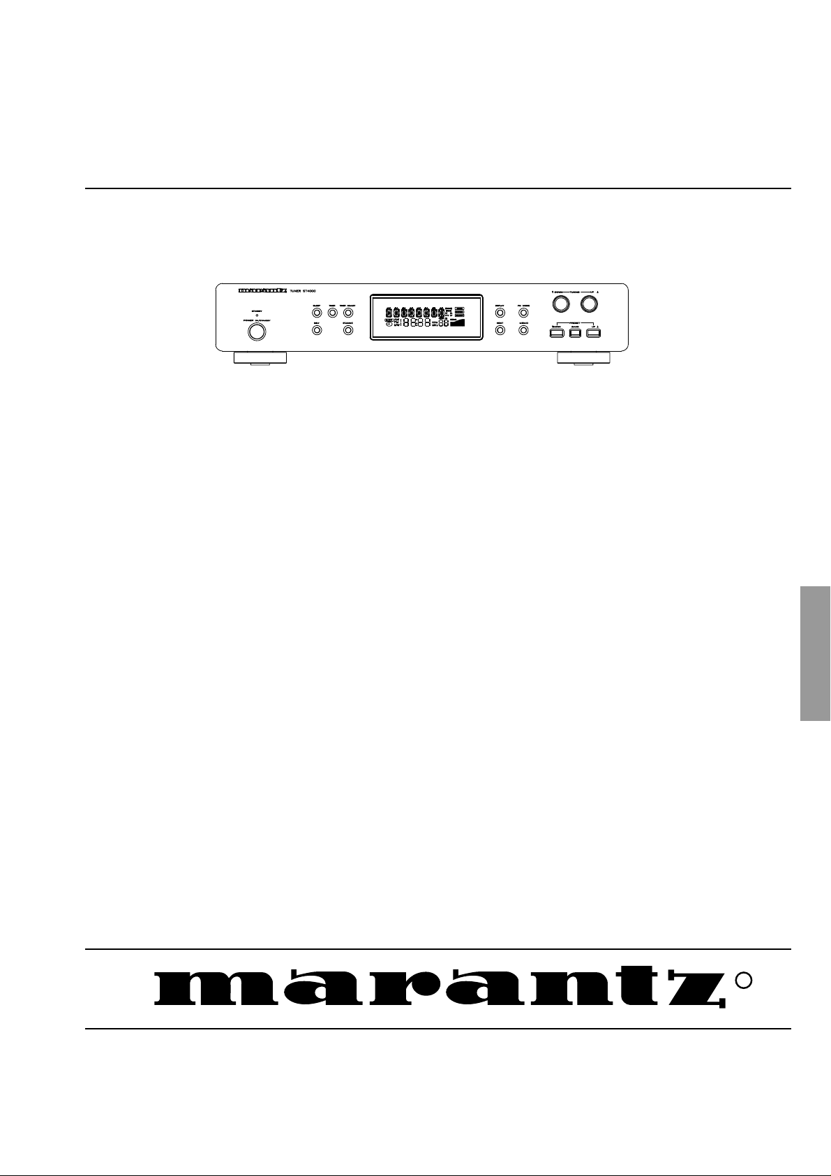
1. TECHNICAL SPECIFICATIONS
FM Section
Tuning Range.....................................................................................................................................87.5 MHz - 108.0 MHz
Usable Sensitivity (IHF) Mono .................................................................................................................................... 10 dBf
50 dB Quieting sensitivity
Mono ................................................................................................................................................................. 17 dBf
Stereo................................................................................................................................................................ 33 dBf
Alternate Channel Selectivity (98 MHz 400 kHz) ...................................................................................................... 65 dB
Image Response Ratio ................................................................................................................................................ 60 dB
Frequency Response ............................................................................................................. 20 Hz - 15 kHz, +0.5 dB/-3 dB
Capture Ratio ................................................................................................................................................... 2 (at 98 MHz)
Distortion (at 65 dBf, 98 MHz)
Mono ...................................................................................................................................................................0.2 %
Stereo..................................................................................................................................................................0.3 %
Signal-to-Noise Ratio (at 65 dBf, 1 kHz)
Mono .................................................................................................................................................................. 70 dB
Stereo................................................................................................................................................................. 65 dB
AM Suppression Ratio ................................................................................................................................................. 80 dB
Stereo Separation (1 kHz) ........................................................................................................................................... 40 dB
Output (Level/Impedance) ........................................................................................................................600 mV/2.2 k ohm
AM Section
Tuning Range.................................................................................................................. 522 kHz - 1,620 kHz (9 kHz steps)
Usable Sensitivity (IHF)................................................................................................. 55 dB/m (562 V/m, Loop Antenna)
Selectivity ..................................................................................................................................................30 dB (at 9 kHz)
Image Response Ratio ................................................................................................................................................ 35 dB
IF Response Ratio ....................................................................................................................................................... 60 dB
Distortion .....................................................................................................................................................1 % (at 85 dB/m)
Signal-to-Noise Ratio ...............................................................................................................................50 dB (at 94 dB/m)
Output (Level/Impedance) ........................................................................................................................170 mV/2.2 k ohm
General
Power Requirements ................................................................................................................................... 230V AC, 50 Hz
Power Consumption........................................................................................................................................................ 6 W
MAX Dimensions (W x H x D) ................................................................................................................. 440 x 86 x 290 mm
Weight (net).................................................................................................................................................................. 3.0 kg
Accessories
AM Loop Antenna x 1, FM Antenna x 1
PCA pin plug cord x 1, Remote control Cable x 1
Improvements may result in specifications and features changing without notice.
1
Page 4
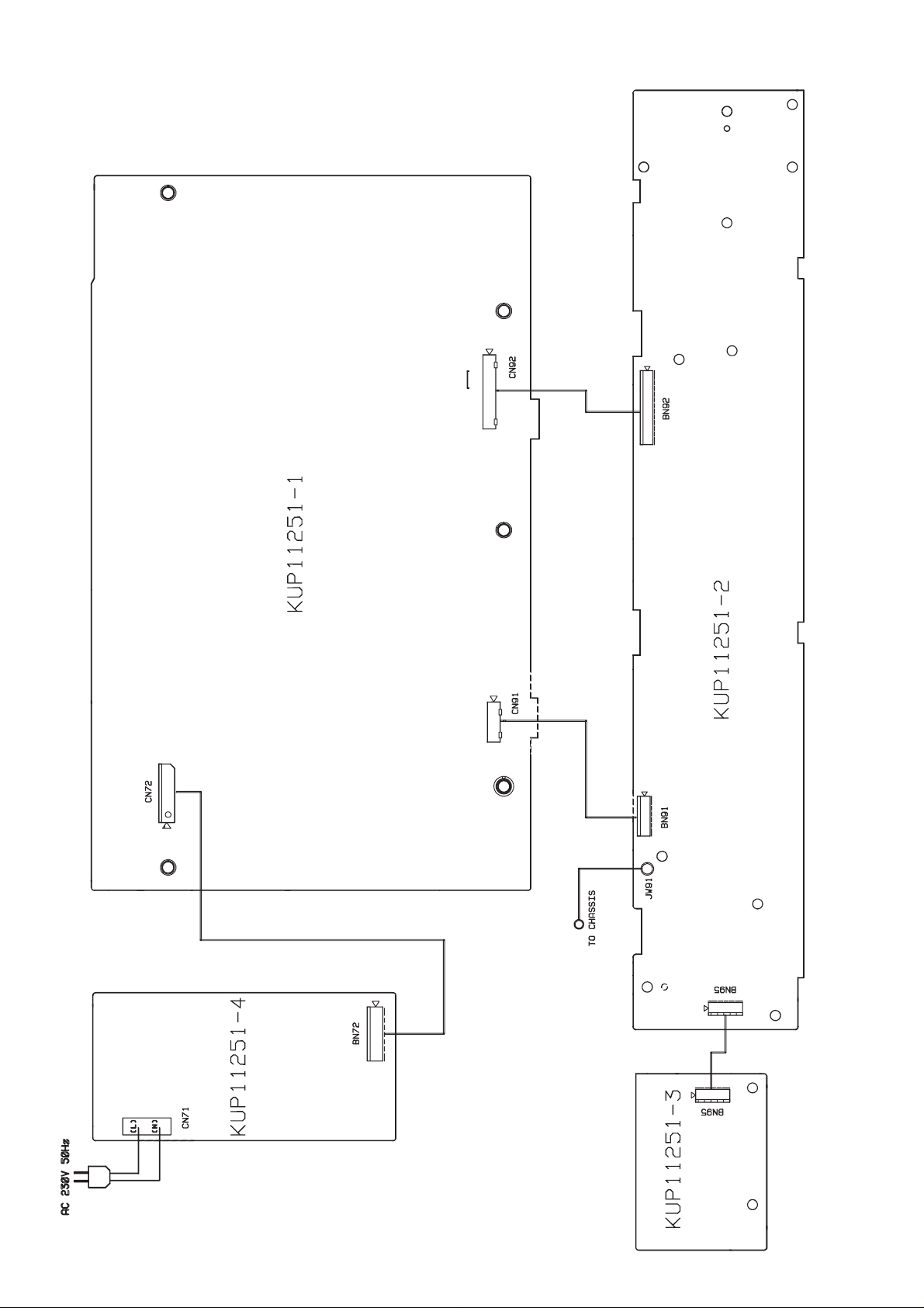
2. WIRING DIAGRAM
RDS-CK
RDS-DR
CE
DI
CK
PLL
DO
ST-IN
TUNED
RESET
GND
5.6V
AM
POWER
GND
REMOTE
FL2
VFIP
FL1
2
Page 5
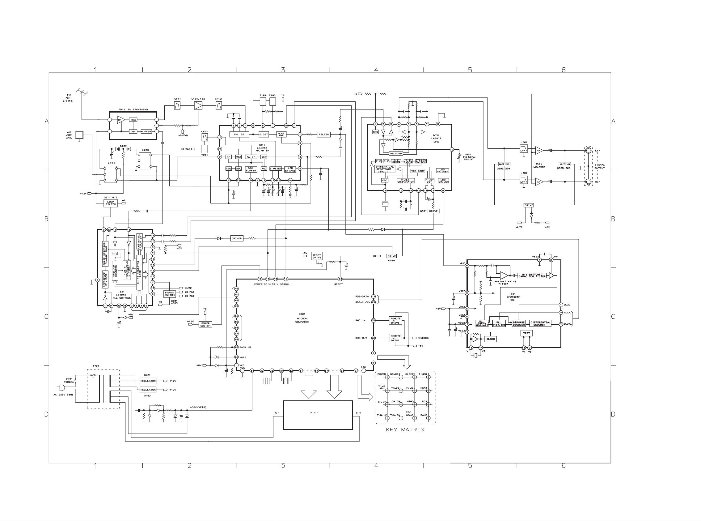
3. BLOCK DIAGRAM
3
4
Page 6

4. SCHEMATIC DIAGRAMS AND PARTS LOCATIONS
5 6
Page 7

7 8
Page 8

Q702
Q701
Q703
Q704
Q307
Q304
Q308
Q303
IC81
Q305
IC31
Q306
Q301
Q503 Q504 IC11 Q502
Q501
Q102
IC51
Q101
Q511
Q512
Q905 Q902 Q901 Q903 IC91
9
Q906
Q908 Q907
10
Page 9

5. MICROPROCESSOR AND IC DATA
1. Block Diagram
IC51 : BVILC7218 (LC7218)
PIN NO. IN/OUT MARK DESCRIPTION OF TERMINAL
1 INPUT XIN Connecting terminal f or crystal oscillator(7.2MHz)
2 INPUT CE Chip enable terminal for seri al data input/output.
3 INPUT DI Data input terminal f or control
4 INPUT CL Clock input terminal for control
5 OUTPUT DO Data output terminal for control
6 INPUT SYS Not used in this unit. ( 0 V )
7 INPUT IN0 Control input for data format
8 INPUT IN1
9 OUTPUT OUT0 Not used in this unit.
10 OUTPUT OUT1 MUTE ON: "H" , MUTE OFF: "L"
11 OUTPUT OUT2 FM : "H" , AM : "L"
12 OUTPUT OUT3 Not used in this unit.
13 OUTPUT OUT4 STEREO : "L" , MONO : "H"
14 OUTPUT OUT5 Signal indicator driver
15 INPUT LCTR Input terminal for IF detector
16 INPUT HCTR
17 OUTPUT OUT6 Output terminal for IF detector
18 INPUT AM IN Input for AM OSC output
19 INPUT FM IN Input for FM OSC output
20 INPUT VDD Power supply terminal
21 OUTPUT PD1 Output terminal for PLL charge pump.
22 OUTPUT PD2 Not us ed i n this unit.
23 - VSS Ground terminal
24 OUTPUT XOUT Connecting terminal for c rystal oscillator(7.2MHz)
IC91 : ANAM 1239T
PIN NO. SYMBOL IN/OUT DESCRIPTION
1 VCC I VDD CONNECTION
2~5 KEY OUT O KEY MATRIX OUTPUT
6~10 N.C NO CONNECTION
11 RDS DA T A I RDS DATA INPUT
12 N.C NO CONNECTION
13 RDS CK I RDS CLOCK INPUT
14~16 GND GROUND
17,18
19 SIGNAL I SIGNAL INPUT
20,21 N.C NO CONNECTION
22,23 GND GROUND
24 VREF I 5V VDD
25 V CC I VDD CONNECTION
26 CE I MICOM CHIP ENABLE
27 GND GROUND
28 TX I
29 TEX O
30 GND GROUND
31 XIN I
32 XOUT O
33 RESET I RESET INPUT
34 RMC-OUT O REMOCON DATA OUTPUT
35,36 RMC-IN I REMOCON DATA INPUT
37~42 N.C NO CONNECTION
43 POWER O TUNER POWER ON/OFF
44 TUNED I TUNED DISPLAY INPUT
45 STEREO I STEREO DISPLAY INPUT
46 PLL DO O PLL SERIAL DATA OUTPUT
47 PLL CK O PLL SERIAL CLOCK OUTPUT
48 PLL DI I PLL SERIAL DATA I NPUT
49 PLL CE O PLL SERIAL CHIP ENA BLE OUTPUT
50 VFIP I FIP VDD : 30V
51~64 G01~G14 O FIP GRIDE SIGNAL OUTPUT
65,66 N.C NO CONNECTION
67~86 P01~P20 O FIP ANODE SIGNAL OUTPUT
87~96 N.C NO CONNECTION
97~100 KEY IN I KEY MATRIX INPUT
AREA
OPTION
I 17(H), 18(H) : EUROPE OPTION
32.768KHz CRISTAL TIME OPERA TOR
8.0MHz CRYSTAL MICOM OPE RA T OR
11
12
Page 10

6. ADJUSTMENT PROCEDURE
(1) ALIGNMENT INSTRUCTIONS
EQUIPMENT NEEDEDIMPORTANT
AM Signal Generator1.Check power-source voltage.
FM Signal Generator2.Set the function switch to band
aligned.
Oscilloscope3.Keep the function input as low as possible
to adjust.
VTVM(AC,DC) accurately.
Test loop antenna (MW Adjustnent) 4.Modulation and
modulation frequency.
Dummy antenna(FM Adjustment)
Stereo signal modulator.
Distortion analyzerModulationModulation Frequency.
EQUIPMENT NEEDEDIMPORTANT
AM Signal Generator1.Check power-source voltage.
FM Signal Generator2.Set the function switch to band
aligned.
Oscilloscope3.Keep the function input as low as possible
to adjust.
VTVM(AC,DC) accurately.
Test loop antenna (MW Adjustnent) 4.Modulation and
modulation frequency.
(3) MW TRACKING ADJUSTMENT
Signal Generator : Connects to the MW Ant.
Coil through the loop antenna.
Adjust for the indication of VTVM of the wave form of
scope to be maximum.
NO STEP
1 612KHz Max sensitivity L102
2 1503KHz Max sensitivity CT01MW
3 Repeat steps 1 and 2 several times.
AM-SG
MHz
60cm
FREQUENCY
AM LOOP antenna
OUTPUT
terminal
ADJUST FOR
AC EVM OSCILLOSCOPE
ADJUS-
MENT
(5) FM MONO DISTORTION ADJUSTMENT
DC VOLTMETER
Connect to TP02 (-),TP03 (+) through the chockcoil
(100 H).
Signal Generator
Connect to FM ANT. Jack (FM IN) through thedummy.
Distortion Meter
Connect to the output.
NO FREQUE NCY ADJUST FOR ADJUSTMENT
1 100.10MHz
2 100.10MHz min T.H.D T102
3 Repeat steps 1 and 2 several times
FM-SG
MHz
OUT
Chassis
DC Voltmeter
0V
UNIT
Choke coil
TP12
TP13
100 H
output
T101
DC EVM
(7) FM/MW TUNED LEVEL ADJUSTMENT
FM Signal Generator : Connect to FM ANT. Jack (FM IN)
through the dummy.
MW Signal Generator : Connect to MW ANT. Coil thriugh
Loop antenna.
BAND STEP SIGNAL GENERATOR ADJUST FOR ADJUSTMENT
FM 1 100.10MHz 30dB TUNED ON VR02
2 100.10MHz 30dB TUNED OFF VR02
MW 1 999KHz 80dB TUNED ON VR01
2 999KHz 80dB TUNED OFF VR01
MODULATION
FREQUENCY
MW
FM
MODULATION
30% 400Hz
100%(75KHz) 400Hz
(2) TUNING FREQUENCY RANGE ADJUSTMENT
(FM) DC VOLTMETER
CONNECT TO TEST POINT TP1 and GND
(MW) DC VOLTMETER
CONNECT TO TEST POINT TP1 and GND
NO BAND
1FM87.50MHz 1.5V L4
2 MW 522KHz 1V L103
FM
AM
GND
FREQUENCY
UNIT
TP11
GND
ADJUST
FOR
ADJUST-
MENT
DC EVM
(4) FM-RF ADJUSTMENT
Signal Generator : Connects to FM ANT. JACK (FM IN)
through the dummy.
NO FREQUENCY ADJUST FOR ADJUSTMENT
1 90.10MHz Max sensitivity L1,L2,L3
2 Repeat step 1 several times
FM-SG
MHz
OUT
75ohm
UNIT
OUTPUT
terminal
FM ANT
AC EVM OSCILLOSCOPE
(6) FM STEREO SEPARATION
PILOT
SIGNAL
ON
FM-SG Dummy UNIT
OUT
EXT
OUT
STEREO
MODULATOR
ADJUST FOR ADJUSTMEN T
Different of R and L
Must be maximum
FM IN OUTPUT
DISTORTION
ANALYSER
VR03
STEREO
OSCILLOSCOPE
VTVM
VR03
13
14
Page 11

ADJUSTMENT POINT
15
Page 12

7. EXPLODED VIEW AND PARTS LIST
(VERS. :VERSION, U:U.S.A. , F:JAPAN, K:FAR EAST, N:EUROPE)
VERS.
POS.
COLOR
NO
1 9965 000 01238 WINDOW FIP 281W158010
2 nsp BADGE MARANTZ nsp
3 9965 000 01242 PANEL FRONT 281W248010
4 9965 000 01243 KNOB POWER 281W270010
5 9965 000 01244 INDICATOR 285W355010
6 9965 000 01245 KNOB TIMER 281W270050
7 9965 000 01246 KNOB TUNING 281W270030
8 9965 000 01247 KNOB DISPLAY 281W270040
9 9965 000 01248 KNOB PRESET 281W270020
10 nsp CABINET TOP nsp
14 nsp HOLDER PCB nsp
15 nsp CHASSIS BOTTOM nsp
16 4822 146 10926 TRANS MAINS 230V *TS000780R
17 nsp BUSHING MAINS CORD nsp
18 nsp MAINS CORD nsp
19 4822 462 10695 FOOT 168W057010
20 nsp RUBBER CUSHION nsp
S1
nsp SCREW nsp
S8
001T 9965 000 01249 MANUAL INSTRUCTION 281W851310
nsp ANT FM WIRE nsp
nsp AM LOOP ANT ASS’Y nsp
PART NO.
(FOR PCS)
PACKING
DESCRIPTION
PART NO.
(MJI)
16
Page 13

8. ELECTRICAL PARTS LIST
ASSIGNMENT OF COMMON PARTS CODES.
RESISTORS
R 1) GD05 x x x 140, Carbon film fixed resistor, 5% 1/4W
R 2) GD05 x x x 160, Carbon film fixed resistor, 5% 1/6W
CAPACITORS
C : CERAMIC CAP.
Examples
:
:
1 Resistance value
Examples
1 Resistance value
0.1 ..... 001 10 ......100 1k ......102 100k ...... 104
0.5 ..... 005 18 ......180 2.7k ......272 680k ...... 684
1 ..... 010 100 ......101 10k ...... 103 1M ...... 105
6.8 ..... 068 390 ......3 9 1 2 2 k ...... 22 3 4.7M ...... 4 7 5
Note : Please distinguish 1/4W from 1/6W by the shape of parts
used actually.
3) DD1 x x x x 370, Ceramic capacitor
Disc type
Temp.coeff. P350~N1000, 50V
3 Capacity value
2 Tolerance
2 Tolerance (Capacity deviation)
0.25 pF ....... 0
0.5 pF ....... 1
5 % .......5
Tolerance of COMMON PARTS handled here are as follows :
0.5 pF - 5 pF ....... 0.25 pF
6 pF - 10 p F ..... 0.5 pF
12 pF - 560 pF ... 5 %
3 Capacity value
0.5 pF .... 0 0 5 3 p F ..... 030 100 pF..... 101
1 pF .... 010 10 p F ..... 100 220 pF..... 221
1.5 pF .... 0 1 5 47 p F ..... 470 560 pF..... 561
NOTE ON SAFETY FOR FUSIBLE RESISTOR :
The suppliers and their type numbers of fusible resistors are as
follows ;
1 . KOA Corporation
Part No.(MJI) Type No.(KOA) Description
NH05 x x x 140 RF25S x x x x
NH05 x x x 120 RF50S x x x x 5% (1/2W)
NH85 x x x 110 RF73B2A x x x x 5% (1/10W)
NH95 x x x 140 RF73B2E x x x x 5% (1/4W)
Resistance value Resistance value(0.1
2. Matsushita Electronic Components Co., Ltd
Part No.(MJI) Type No.(MEC) Description
NF05 x x x 140 ERD-2FCJ x x x ( 5% 1/4W)
RF05 x x x 140
NF02 x x x 140 ERD-2FCG x x x ( 2% 1/4W)
RF02 x x x 140
Examples
Resistance value
0.1 ..... 001 10 ..... 100 1k ..... 102 100k ..... 104
0.5 ..... 005 18 ..... 180 2.7k ..... 272 680k ..... 684
1 ..... 010 100 ..... 101 10k ..... 103 1M ..... 105
6.8 ..... 068 390 ..... 391 22k ..... 223 4.7M ..... 475
5% (1/4W)
J
J
J
J
- 10k )
Resistance value
C : CERAMIC CAP.
Examples
4 Capacity value
C : 5) ELECTROLY CAP.( ), 6)FILM CAP ( )
Examples
5 Capacity value
6 Working voltage
Examples
7 Capacity value
4) DK16 x x x 300, High dielectric constant ceramic
4 Capacity value
100 pF .....101 1000 pF .... 102 10000 pF .... 103
470 pF .....471 2200 pF .... 222
5) EA x x x x x x 10, Electrolytic capacitor
5 Capacity value
0.1 F .... 104 4.7 F .... 47 5 100 F .....10 7
0.33 F .... 334 10 F .... 106 3 3 0 F .....33 7
1 F .... 105 22 F .... 2 2 6 1100 F .....118
2200 F .... 228
6.3 V ...... 0 0 6 2 5 V ..... 0 2 5
10 V ...... 01 0 3 5 V ..... 0 3 5
16 V ...... 01 6 5 0 V ..... 050
6) DF15 x x x 350 Plastic film capacitor
DF15 x x x 310 One-way type, Mylar 5% 50V
DF16 x x x 310 Plastic film capacitor
7 Capacity value
F (1000 pF) ...... 1 0 2 0.1 F ...... 10 4
0.001
0.0018
F........................ 18 2 0.56 F ......564
F........................ 10 3 1 F...... 10 5
0.01
F........................ 15 3
0.015
capacitor
Disc type
Temp.chara. 2B4, 50V
One-way lead type,Tolerance 20%
6 Working voltage
One-way type, Mylar 10% 50V
ABBREVIA
ANT . : ANTENNA BATT . : BATTERY
CAP. : CAPACITOR CER. : CERAMIC
CONN. : CONNECTING DIG. : DIGITAL
HP : HEADPHONE MIC. : MICROPHONE
-PRO : MICROPROCESSOR REC. : RECORDING
RES. : RESISTOR SPK : SPEAKER
SW : SWITCH TRANSF. : TRANSFORMER
TRIM. : TRIMMING TRS. : TRANSISTOR
VAR. : VARIABLE X’ TAL : CRYSTAL
TION AND MARKS
NOTE ON SAFETY:
Symbol Fire or electrical shock hazard. Only original
parts should be used to replaced any part marked with
symbol Any other component substitution ( other than
original type), may increase risk of fire or electrical shock
hazard.
NOTE
1) The above CODES(R ,R ,C ,C
and C ) are omitted on the schematic diagram in
some case.
2) On the occasion, be confirmed the common parts on the
parts list.
3) Refer to “Common Parts List” for the other common
parts(Rl05, DD4, DK4).
17
990521 A.O
Page 14

(VERS. :VERSION, U:U.S.A. , F:JAPAN, K:FAR EAST, N:EUROPE)
POS.
NO
VERS.
COLOR
PART NO.
(FOR PCS)
DESCRIPTION
PART NO.
(MJI)
(VERS. :VERSION, U:U.S.A. , F:JAPAN, K:FAR EAST, N:EUROPE)
POS.
NO
VERS.
COLOR
PART NO.
(FOR PCS)
DESCRIPTION
PART NO.
(MJI)
CF21 4822 242 10853 FILM SFZ450F FF10045290
CF11 4822 242 11039 FILM SFE10.7MS8H-A-T *FF100230R
CF12 4822 242 11039 FILM SFE10.7MS8H-A-T *FF100230R
CG91 4822 124 12129 ELECT 0.1F *EX000030R
CT21 4822 125 11116 TRIM. VARIABLE *CT000110R
C102 nsp CER. 15pF 50V J nsp
C105 nsp CER. 0.01 F 50V Z nsp
C106 nsp CER. 15pF 50V J nsp
C107 nsp CER. 15pF 50V J nsp
C108 nsp CER. 10pF 50V J nsp
C109 nsp CER. 0.01 F 50V Z nsp
C110 nsp CER. 0.1 F 50V Z nsp
C111 nsp CER. 0.1 F 50V Z nsp
C112 nsp ELECT 1 F 50V nsp
C113 nsp CER. 0.01 F 50V Z nsp
C114 nsp ELECT 220 F 16V nsp
C115 nsp ELECT 4.7 F 50V nsp
C116 nsp CER. 33pF 50V J nsp
C117 nsp CER. 390pF 50V K nsp
C118
nsp CER. 100pF 50V K nsp
C121
C123 nsp ELECT 1 F 50V nsp
C201 nsp CER. 0.1 F 50V Z nsp
C202 nsp CER. 15pF 50V J nsp
C203 nsp CER. 470pF 50V K nsp
C204 nsp CER. 0.1 F 50V Z nsp
C205 nsp ELECT 100 F 16V nsp
C206 nsp CER. 0.001 F 50V K nsp
C207 nsp CER. 0.1 F 50V Z nsp
C208 nsp CER. 8.2pF 50V J nsp
C209 nsp CER. 47pF 50V J nsp
C210 nsp ELECT
C211 nsp ELECT
C212 nsp ELECT
C213 nsp CER.
C214 nsp FILM
C215 nsp FILM
C301 nsp ELECT 10 F 50V nsp
C302 nsp ELECT 220 F 16V nsp
C303 nsp CER. 0.1 F 50V Z nsp
C304 nsp ELECT 0.47 F 50V nsp
C305 nsp ELECT 3.3 F 50V nsp
C306 nsp ELECT 10 F 50V nsp
C307 nsp ELECT 1 F 50V nsp
C308 nsp ELECT 1 F 50V nsp
C309 nsp ELECT 100 F 16V nsp
C310 nsp ELECT 10 F 50V nsp
C311 nsp ELECT 1 F 50V nsp
C312 nsp CER. 100pF 50V K nsp
C313 nsp CER. 470pF 50V K nsp
C315 nsp CER. 560pF 50V K nsp
C316 nsp CER. 560pF 50V K nsp
C317 nsp ELECT 4.7 F 50V nsp
C318 nsp ELECT 4.7 F 50V nsp
C319 nsp ELECT 2.2 F 50V nsp
C320 nsp ELECT 2.2 F 50V nsp
C321 nsp ELECT 10 F 50V nsp
C322 nsp ELECT 10 F 50V nsp
C323 nsp ELECT 4.7 F 50V nsp
C324 nsp ELECT 4.7 F 50V nsp
C325 nsp FILM 0.0015 F 50V J nsp
C326 nsp FILM 0.0015 F 50V J nsp
C501 nsp CER. 0.01 F 50V Z nsp
C502 nsp ELECT 470 F 10V nsp
C503 nsp CER. 33pF 50V J nsp
C504 nsp CER. 33pF 50V J nsp
CAPACITORS
4.7
0.0047
0.0015
0.027
F 50V nsp
1
F 50V nsp
F 50V nsp
1
F 50V M nsp
F 50V J nsp
F 50V J nsp
C505
nsp CER. 100pF 50V K nsp
C508
C510 nsp CER. 0.022 F 50V Z nsp
C511 nsp ELECT 4.7 F 50V nsp
C512 nsp CER. 0.022 F 50V Z nsp
C515 nsp CER. 0.01 F 50V Z nsp
C516 nsp CER. 5.6pF 50V K nsp
C531 nsp CER. 0.022 F 50V Z nsp
C532 nsp CER. 0.022 F 50V Z nsp
C701 nsp CER. 680pF 50V K nsp
C702 nsp CER. 680pF 50V K nsp
C703 4822 124 41334 ELECT 470 F 35V EA47703510
C704 4822 124 41334 ELECT 470 F 35V EA47703510
C705 9965 000 01264 ELECT 2200 F 25V EA22802510
C706 nsp CER. 0.01 F 50V Z nsp
C707 nsp ELECT 330 F 25V nsp
C708 nsp CER. 0.01 F 50V Z nsp
C709 nsp ELECT 100 F 16V nsp
C711 nsp ELECT nsp
C712 nsp CER. 680pF 50V K nsp
C713 nsp CER. 680pF 50V K nsp
C714 nsp ELECT 47 F 50V
C715 nsp ELECT 47 F 50V nsp
C716 nsp ELECT 3.3 F 50V nsp
C720 nsp CER. 0.022 F 50V Z nsp
C801 nsp CER. 390pF 50V K nsp
C802 nsp CER. 0.01 F 50V Z nsp
C803 nsp ELECT 100 F 16V nsp
C804 nsp CER. 33pF 50V J nsp
C805 nsp CER. 39pF 50V J nsp
C806 nsp ELECT 10 F 50V nsp
C807 nsp CER. 100pF 50V K nsp
C808 nsp CER. 0.022 F 50V Z nsp
C809 nsp CER. 0.022 F 50V Z nsp
C901 nsp CER. 0.1 F 50V Z nsp
C902 nsp CER. 0.022 F 50V Z nsp
C903 nsp ELECT 100 F 10V nsp
C905 nsp ELECT 1000 F 6.3V nsp
C907 nsp CER. 18pF 50V J nsp
C908 nsp CER. 12pF 50V J nsp
C909 nsp ELECT 22 F 16V nsp
C910 nsp ELECT 10 F 16V nsp
C911 nsp CER. 22pF 50V J nsp
C912 nsp CER. 18pF 50V J nsp
C921 nsp CER. 0.022 F 50V Z nsp
D201 9965 000 01250 1SS131M *HD201290R
D203 9965 000 01250 1SS131M *HD201290R
D302 9965 000 01250 1SS131M *HD201290R
D303 9965 000 01250 1SS131M *HD201290R
D501 9965 000 01250 1SS131M *HD201290R
D202 nsp VARICAP SVC342-L-AA *HD400160R
D502 9965 000 01250 1SS131M *HD201290R
D503 9965 000 01250 1SS131M *HD201290R
D701 4822 130 31878 1N4003 HD200010AR
D702 4822 130 31878 1N4003 HD200010AR
D703 4822 130 11131 ZENER 13V 1/2W *HD301430R
D704 4822 130 11132 ZENER 6.2V 1/2W *HD301450R
D711 4822 130 31878 1N4003 HD200010AR
D712 4822 130 31878 1N4003 HD200010AR
D713 9965 000 01260 ZENER 24V UZ24BMT *HD301700R
D714 4822 130 11132 ZENER 6.2V 1/2W *HD301450R
D801 9965 000 01250 1SS131M *HD201290R
D901 9965 000 01250 1SS131M *HD201290R
D902 4822 130 11608 LED SLR342VCF02 *HI100810R
D903 9965 000 01250 1SS131M *HD201290R
DIODES
47 F 50V
nsp
18
Page 15

(VERS. :VERSION, U:U.S.A. , F:JAPAN, K:FAR EAST, N:EUROPE)
POS.
NO
VERS.
COLOR
PART NO.
(FOR PCS)
DESCRIPTION
PART NO.
(MJI)
(VERS. :VERSION, U:U.S.A. , F:JAPAN, K:FAR EAST, N:EUROPE)
POS.
NO
VERS.
COLOR
PART NO.
(FOR PCS)
DESCRIPTION
PART NO.
(MJI)
D905 9965 000 01250 1SS131M *HD201290R
D906 9965 000 01250 1SS131M *HD201290R
D907 9965 000 01250 1SS131M *HD201290R
IC11 4822 209 71785 LA1266 HC10222030
IC31 4822 209 70261 LA3410 HC10198030
IC32 9965 000 01265 KA4558D *HC105110R
IC51 4822 209 30178 LC7218 HC10211032
IC81 4822 209 17453 BFU1923F *HC104810R
IC91 4822 209 16159 MICROPROCESSOR
F701 nsp HOLDER FUSE nsp
L102 4822 157 11873 COIL *LC107220R
L201 nsp COIL 6.8 H K nsp
L202 9965 000 01253 COIL AM ANT3 *TC000360R
L203 4822 157 11484 COIL AM OSC *LO000060R
L301 4822 157 11487 COIL MPX *LS000060R
L302 4822 157 11487 COIL MPX *LS000060R
L701 9965 000 01235 COIL INDUCTOR *TC000350R
Q101 4822 130 63385 KTC3192O *HT300480R
Q102 4822 130 63385 KTC3192O *HT300480R
Q301 4822 130 62503 DTC114YS *BA000730R
Q303 4822 130 63659 DTC143TS *BA000700R
Q304 4822 130 63659 DTC143TS *BA000700R
Q305 4822 130 63659 DTC143TS *BA000700R
Q306 4822 130 63659 DTC143TS *BA000700R
Q307 4822 130 42682 DTA144ES BA10010210
Q308 4822 130 61187 DTA144TS BA10009210
Q501 4822 130 61189 DTC114TS BA20017210
Q502 4822 130 62787 DTA114YS *BA000190R
Q503 4822 130 62787 DTA114YS *BA000190R
Q504 4822 130 61189 DTC114TS BA20017210
Q511 4822 130 42431 2SC1740SR HT317401L0
Q512 4822 130 42431 2SC1740SR HT317401L0
Q701 4822 130 11135 KSD288Y *HT400350R
Q702 9965 000 01254 KTC3227Y *HT300490R
Q703 4822 130 11136 KTA1274Y *HT100320R
Q704 4822 130 42594 DTC144ES BA20012210
Q901 4822 130 62503 DTC114YS *BA000730R
Q902 4822 130 62787 DTA114YS *BA000190R
Q903 4822 130 62503 DTC114YS *BA000730R
Q905 4822 130 62787 DTA114YS *BA000190R
Q906 4822 130 60107 2SA933SR HT109331S0
Q907 4822 130 62503 DTC114YS *BA000730R
Q908 4822 130 62787 DTA114YS *BA000190R
R103 nsp 47 1/5W J nsp
R104 nsp 390 1/5W J nsp
R105 nsp 1.2k 1/5W J nsp
R106 nsp 820k 1/5W J nsp
R107 nsp 560 1/5W J nsp
R108 nsp 470k 1/5W J nsp
R109 nsp 270 1/5W J nsp
R110 nsp 1.8k 1/5W J nsp
R111 nsp 1.5k 1/5W J nsp
R112 nsp 5.6k 1/5W J nsp
R115 nsp 15k 1/5W J nsp
R116 nsp 2.7k 1/5W J nsp
R117 nsp 15k 1/5W J nsp
R118 nsp 2.7k 1/5W J nsp
INTEGRATED CIRCUITS
ANAM1239T
FUSE
COILS
TRANSISTORS
RESISTORS
*HU243WT0R
R119 nsp 1k 1/5W J nsp
R125 nsp 10 1/5W J nsp
R201 nsp 1k 1/5W J nsp
R202 nsp 100k 1/5W J nsp
R203 nsp 470 1/5W J nsp
R204 nsp 100k 1/5W J nsp
R205 nsp 10k 1/5W J nsp
R206 nsp 22k 1/5W J nsp
R207 nsp 22k 1/5W J nsp
R208 nsp 82 1/5W J nsp
R209 nsp 100k 1/5W J nsp
R301 nsp 3.9k 1/5W J nsp
R302 nsp 47 1/5W J nsp
R303 nsp 1k 1/5W J nsp
R304 nsp 10k 1/5W J nsp
R305 nsp 6.8k 1/5W J nsp
R306 nsp 22k 1/5W J nsp
R307 nsp 270 1/5W J nsp
R308 nsp 10k 1/5W J nsp
R309 nsp 10k 1/5W J nsp
R310 nsp 3.9k 1/5W J nsp
R311 nsp 1k 1/5W J nsp
R312 nsp 560 1/5W J nsp
R313 nsp 220k 1/5W J nsp
R315 nsp 91k 1/5W J nsp
R316 nsp 91k 1/5W J nsp
R317 nsp 150k 1/5W J nsp
R318 nsp 150k 1/5W J nsp
R319 nsp 10k 1/5W J nsp
R320 nsp 10k 1/5W J nsp
R321
nsp 3.3k 1/5W J nsp
R324
R325 nsp 100k 1/5W J nsp
R326 nsp 100k 1/5W J nsp
R327 nsp 3.3k 1/5W J nsp
R328 nsp 3.3k 1/5W J nsp
R329 nsp 1.1k 1/5W J nsp
R330 nsp 1.1k 1/5W J nsp
R331 nsp 100 1/5W J nsp
R332 nsp 100 1/5W J nsp
R333 nsp 100k 1/5W J nsp
R334 nsp 100k 1/5W J nsp
R335 nsp 100 1/5W J nsp
R336 nsp 100 1/5W J nsp
R501 nsp 1k 1/5W J nsp
R502 nsp 10k 1/5W J nsp
R505
nsp 10k 1/5W J nsp
R508
R510 nsp 1k 1/5W J nsp
R511 nsp 560 1/5W J nsp
R512 nsp 5.6k 1/5W J nsp
R513 nsp 10k 1/5W J nsp
R520
nsp 10k 1/5W J nsp
R524
R525 nsp 470k 1/5W J nsp
R527 nsp 10k 1/5W J nsp
R531 nsp 470k 1/5W J nsp
R532 nsp 470k 1/5W J nsp
R533 nsp 10k 1/5W J nsp
R601 nsp 10k 1/5W J nsp
R602 nsp 10k 1/5W J nsp
R701 9965 000 01262 27 1/2W J FUSE *NH000100R
R702 nsp 1k 1/5W J nsp
R703 nsp 100 1/5W J nsp
R704 nsp 1k 1/5W J nsp
R705 nsp 100 1/5W J nsp
19
Page 16

(VERS. :VERSION, U:U.S.A. , F:JAPAN, K:FAR EAST, N:EUROPE)
VERS.
POS.
COLOR
NO
R707 nsp 47k 1/5W J nsp
R708 nsp 18k 1/5W J nsp
R709 nsp 4.7k 1/5W J nsp
R711 nsp 330 1/5W J nsp
R712 nsp 47k 1/5W J nsp
R713 nsp 4.7 1/5W J nsp
R714 nsp 47k 1/5W J nsp
R715 nsp 3.3 1/5W J nsp
R716 nsp 3.3 1/5W J nsp
R801 nsp 10 1/5W J nsp
R802 nsp 470 1/5W J nsp
R805 nsp 1k 1/5W J nsp
R806 nsp 1k 1/5W J nsp
R901 nsp 1k 1/5W J nsp
R902 nsp 470 1/5W J nsp
R903 nsp 100k 1/5W J nsp
R905 nsp 1k 1/5W J nsp
R906 nsp 22k 1/5W J nsp
R907 nsp 47k 1/5W J nsp
R908 nsp 47k 1/5W J nsp
R909 nsp 47k 1/5W J nsp
R910 nsp 100k 1/5W J nsp
R911 nsp 10k 1/5W J nsp
R912 nsp 47k 1/5W J nsp
R913 nsp 47k 1/5W J nsp
R915
nsp 47k 1/5W J nsp
R924
R951 nsp 3.3 1/5W J nsp
PART NO.
(FOR PCS)
DESCRIPTION
PART NO.
(MJI)
(VERS. :VERSION, U:U.S.A. , F:JAPAN, K:FAR EAST, N:EUROPE)
POS.
NO
VERS.
COLOR
PART NO.
(FOR PCS)
DESCRIPTION
PART NO.
(MJI)
S601 4822 276 14107 SW. TACT *SP000880R
S911 9965 000 01263 SW. TACT *SP000890R
S913
9965 000 01263 SW. TACT *SP000890R
S926
CN71 nsp 7.92MM(YUNHO) nsp
CN72 nsp MOLEX 5267-07A nsp
CN91 nsp MOLEX53014-0610 nsp
CN92 nsp WAFER nsp
BN72 nsp WIRE ASS’Y nsp
BN91 nsp WIRE ASS’Y nsp
BN92 nsp WIRE ASS’Y nsp
BN95 nsp WIRE ASS’Y nsp
FIP1 9965 000 01234 FLD SVA-14MM11 *HQ300380R
FP11 4822 210 10802 TUNER PACK FTA4460H *AV000060R
JK11 4822 265 11601 TERMINAL ANT.SC0210392N *YT001500R
JK31 4822 265 11205 RCA JACK 2P KC S436P *YT001170R
JK32 4822 265 11206 RCA JACK 2P ORANGE *YT001180R
JW91 nsp WIRE ASS’Y nsp
T101 4822 157 11861 IFT FM *LA000110R
T102 4822 157 11489 IFT FM *LI000070R
T201 9965 000 01267 IFT AM *TC000370R
T701 4822 146 10926 TRANS MAINS 230V *TS000780R
VR21 4822 101 11853 RES.TRIM EVNDJAA03B24 *RA000790R
VR31 9965 000 01270 RES.TRIM EVNDJAA03B15 *RA000930R
VR11 9965 000 01271 RES.TRIM EVNDJAA03B54 *RA000940R
SWITCHES
MISCELLANEOUS
X201 4822 242 82242 CER. FIL. BFU450C4N *FF100190R
X301 4822 242 81117 RESONATOR CSB456F11 FQ04563010
X501 4822 242 72333 CRYSTAL 7.2MHz JX07001261
X801 4822 242 11042 CRYSTAL 4.332MHz *JX000540R
X901 4822 242 10855 CRYSTAL 8MHz *JX000410R
X902 4822 242 72236 CRYSTAL 32 768kHz DT-38 XO001001T2
20
 Loading...