

Page 1
Service
MD110/F1S / N1S
Manual
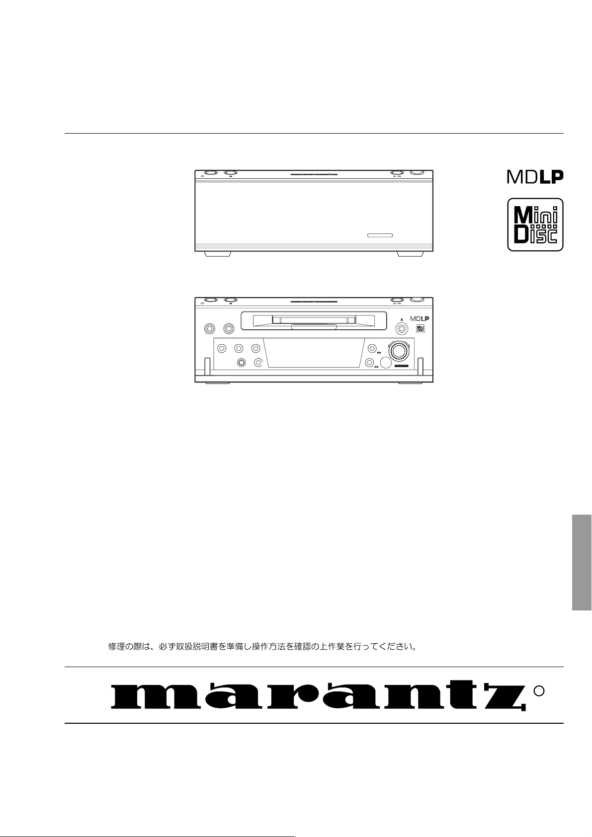
STANDBY OPEN
MD110
STANDBY OPEN
DISPLAY
SOURCE
DUBB.
CHARACTER
REC
EDIT
MULTI JOG
PUSH ENTER
REC MODE
MD Deck
TABLE OF CONTENTS
SECTION PAGE
1. TECHNICAL SPECIFICATIONS ........................................................................... 1
2. SERVICE MODE .................................................................................................. 2
3. WIRING DIAGRAM ............................................................................................... 9
4. BLOCK DIAGRAM .............................................................................................. 11
5. SCHEMATIC DIAGRAM ..................................................................................... 13
6. PARTS LOCATION (Pattern Side) ..................................................................... 15
7. IC DATA .............................................................................................................. 21
8. EXPLODED VIEW AND PARTS LIST ................................................................ 27
9. ELECTRICAL PARTS LIST ................................................................................ 32
Please use this service manual with referring to the user guide ( D.F.U. ) without fail.
MD110
R
MD110
325W855010 MIT
3120 785 22730
First Issue 2001.12
Page 2
MARANTZ DESIGN AND SERVICE
MARANTZ AMERICA, INC.
Using superior design and selected high grade components, MARANTZ company has created the ultimate in stereo sound.
Only original MARANTZ parts can insure that your MARANTZ product will continue to perform to the specifications for which
it is famous.
Parts for your
MARANTZ equipment are generally available to our National Marantz Subsidiary or Agent.
ORDERING PARTS :
Parts can be ordered either by mail or by Fax.. In both cases, the correct part number has to be specified.
The following information must be supplied to eliminate delays in processing your order :
1. Complete address
2. Complete part numbers and quantities required
3. Description of parts
4. Model number for which part is required
5. Way of shipment
6. Signature : any order form or Fax. must be signed, otherwise such part order will be considered as null and void.
USA
MARANTZ AMERICA, INC
1100 MAPLEWOOD DRIVE
ITASCA, IL. 60143
USA
PHONE : 630 - 741 - 0300
FAX : 630 - 741 - 0301
AMERICAS
SUPERSCOPE TECHNOLOGIES, INC.
MARANTZ PROFESSIONAL PRODUCTS
2640 WHITE OAK CIRCLE, SUITE A
AURORA, ILLINOIS 60504 USA
PHONE : 630 - 820 - 4800
FAX : 630 - 820 - 8103
AUSTRALIA
QualiFi Pty Ltd,
24 LIONEL ROAD,
MT. WAVERLEY VIC 3149
AUSTRALIA
PHONE : +61 - (0)3 - 9543 - 1522
FAX : +61 - (0)3 - 9543 - 3677
NEW ZEALAND
WILDASH AUDIO SYSTEMS NZ
14 MALVERN ROAD MT ALBERT
AUCKLAND NEW ZEALAND
PHONE : +64 - 9 - 8451958
FAX : +64 - 9 - 8463554
EUROPE / TRADING
MARANTZ EUROPE B.V.
P.O.BOX 80002, BUILDING SFF2
5600 JB EINDHOVEN
THE NETHERLANDS
PHONE : +31 - 40 - 2732241
FAX : +31 - 40 - 2735578
AUSTRALIA
TECHNICAL AUDIO GROUP PTY, LTD
558 DARLING STREET,
BALMAIN, NSW 2041,
AUSTRALIA
PHONE : 61 - 2 - 9810 - 5300
FAX : 61 - 2 - 9810 - 5355
THAILAND
MRZ STANDARD CO.,LTD
746 - 754 MAHACHAI ROAD.,
WANGBURAPAPIROM, PHRANAKORN,
BANGKOK, 10200 THAILAND
PHONE : +66 - 2 - 222 9181
FAX : +66 - 2 - 224 6795
TAIWAN
PAI- YUING CO., LTD.
6 TH FL NO, 148 SUNG KIANG ROAD,
TAIPEI, 10429, TAIWAN R.O.C.
PHONE : +886 - 2 - 25221304
FAX : +886 - 2 - 25630415
BRAZIL
PHILIPS DA AMAZONIA IND. ELET. ITDA
CENTRO DE INFORMACOES AO
CEP 04698-970
SAO PAULO, SP, BRAZIL
PHONE : 0800 - 123123
FAX : +55 11 534. 8988
(Discagem Direta Gratuita)
CANADA
LENBROOK INDUSTRIES LIMITED
633 GRANITE COURT,
PICKERING, ONTARIO L1W 3K1
CANADA
PHONE : 905 - 831 - 6333
FAX : 905 - 831 - 6936
SINGAPORE
WO KEE HONG DISTRIBUTION PTE LTD
130 JOO SENG ROAD
#03-02 OLIVINE BUILDING
SINGAPORE 368357
PHONE : +65 858 5535 / +65 381 8621
FAX : +65 858 6078
MALAYSIA
WO KEE HONG ELECTRONICS SDN. BHD.
SUITE 8.1, LEVEL 8, MENARA GENESIS,
NO. 33, JALAN SULTAN ISMAIL,
50250 KUALA LUMPUR, MALAYSIA
PHONE : +60 3 - 2457677
FAX : +60 3 - 2458180
JAPAN
MARANTZ JAPAN, INC.
Technical
35- 1, 7- CHOME, SAGAMIONO
SAGAMIHARA - SHI, KANAGAWA
JAPAN 228-8505
PHONE : +81 42 748 1013
FAX : +81 42 741 9190
KOREA
MK ENTERPRISES LTD.
ROOM 604/605, ELECTRO-OFFICETEL, 16-58,
3GA, HANGANG-RO, YONGSAN-KU, SEOUL
KOREA
PHONE : +822 - 3232 - 155
FAX : +822 - 3232 - 154
SHOCK, FIRE HAZARD SERVICE TEST :
CAUTION : After servicing this appliance and prior to returning to customer, measure the resistance between either primary AC
cord connector pins ( with unit NOT connected to AC mains and its Power switch ON ), and the face or Front Panel of product and
controls and chassis bottom.
Any resistance measurement less than 1 Megohms should cause unit to be repaired or corrected before AC power is applied, and
verified before it is return to the user/customer.
Ref. UL Standard No. 1492.
In case of difficulties, do not hesitate to contact the Technical
Department at above mentioned address.
010620MIT
Page 3

1. TECHNICAL SPECIFICATIONS
MAIN UNIT (MD110)
Type ........................................................................................................................... MiniDisc Digital Audio System
Laser ......................................................................................................................................... Semiconductor laser
Recording method ............................................................................... Magnetic field modulation overwrite method
RPMs ......................................................................................................... Approximately 400rpm to 900rpm (CLV)
Sampling frequency .....................................................................................................................................44.1 kHz
Frequency characteristics ........................................................................................................ 20 to 20 kHz (± 1 dB)
S/N .................................................................................................................................................. 85 dB or greater
Total Harmonic Distortion ................................................................................................................. 0.005 % or less
Wow and Flutter............................................................................................................ Less than measurable limits
Line output level.......................................................................................................................................... 2.0 Vrms
Analog Input ........................................................................................................................................... 250 mVrms
GENERAL
Power supply ......................................................................................................... AC 100 V 50 / 60 Hz (F version)
AC 230 V 50 Hz (N version)
Power Consumption <Electric Appliance Control Act> ......................................................................................16 W
Maximum external dimensions (W x H x D)............................................................................. 210 x 71.5 x 310 mm
Weight.............................................................................................................................................................. 3.3 kg
ACCESSORIES
Remote Control Transmitter (RC110DRMD/N1S, RC110DRMDF/F1S) ..................................................................1
External dimensions (W x H x D) ........................................................................................ 50.5 x 154.5 x 25 mm
Weight ............................................................................................................................................................. 60 g
AA type batteries ..................................................................................................................................................... 2
Stereo audio cable ............................................................................................................................................ 1 pair
Coaxial cable ........................................................................................................................................................... 1
Remote control cable ............................................................................................................................................... 1
The specifications and external appearance are subject to change without notice.
Some portions of the illustrations that appear in this manual may differ slightly from the actual product.
This product is licensed under U.S. and foreign patents of Dolby Laboratories.
1
Page 4
2. SERVICE MODE
Service Mode
1. While Mains cord is disconnected, press DISPLAY Button on the unit and plug in the Mains cord.
2. Version number of the front micom software is displayed.
3. Turn JOG dial to either direction then Display segment test begins.
4. First all the segments will light and then a segment turns off one by one.
5. Disconnect Mains cord to quit service mode.
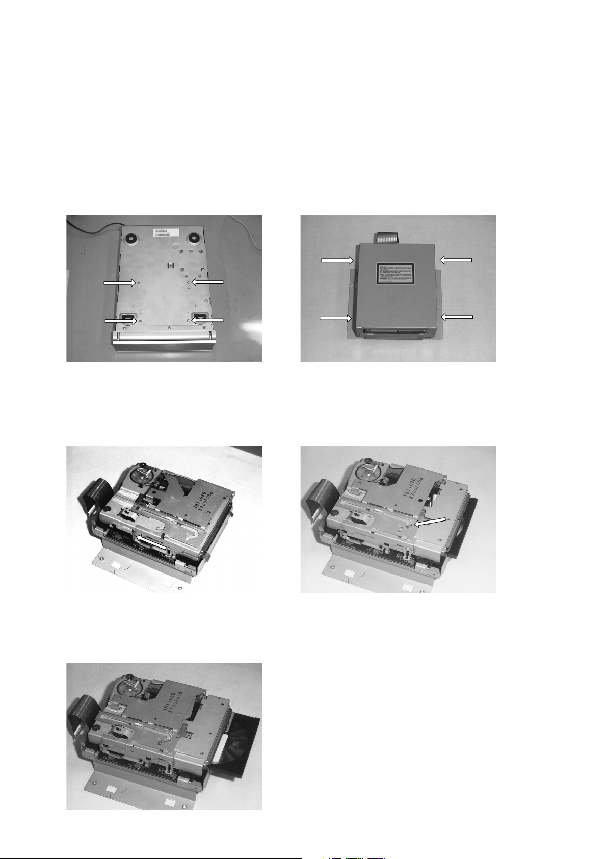
Emargency Eject
1. Remove 5 screws on the top cover and remove 3. Disconnect the flexible wire.
the top cover. 4. Remove the MD mechanism component from the
2. Remove 4 screws on the bottom. (Pointed with unit and remove the 4 screws on the both sides.
the arrows in the picture above.) (Pointed with the arrows in the picture above.)
5. Slide the lever pointed with the arrow to the direction 6. Slide the pin pointed with the arrow to the direction
of the arrow. of the arrow.
7. Disc is ejected.
2
Page 5
TEST MODE
1 How to Setting and Cancel Test Mode
Setting: While pressing the PLAY/PAUSE keys, insert the power cord to the wall outlet.
Cancel: Pull out the power cord.
Key Operation for Adjustment
Key Operation
MULTI JOG Select parameter and mode.
PLAY Fix items. Change of display in every check.
STOP Cancel or back of test mode.
2 Remained Keys Operation
Key Operation
DISPLAY Display changes.
FF Pickup moves outwards when press FF key
FB Pickup moves inwards when press FB key
3 Selection of test mode
13 test modes are selected by pressing UPIDOWN keys.
No. Display Description Section
1 TEMP ADJUST The work of adjustment is unnecessary in this mode 6-5
2 LDPWR ADJUST Laser power adjustment 6-6
3 LDPWR CHECK Laser power check 6-6
4 EFBAL ADJUST Traverse adjustment 6-7
5 TE B. ADJUST Automatic EF balance adjustment
6 FBIAS ADJUST Focus bias adjustment 6-8
7 CPLAY MODE Continuous playback mode 5-4
8 CREC MODE Continuous recording mode 5-5
9 STT-LIMIT SW Check the mechanism start limit SW position 10 JUMP MODE Track jump checking mode 11 SRV DAT READ Servo data reading 12 EEP MODE E2PROM data reading or rewrite -
13 EEP INITIAL E2PROM data initializing For more information on each adjustment mode, refer to each section of 6, "Electrical adjustment".
If other adjustment mode has been entered incorrectly, press the STOP key to exit the mode.
*The number 9 -13 are not used for service. If these modes have been entered incorrectly, press the STOP key
immediately to exit the mode. Specially, do not use EEP INITIAL. (E2PROM data has initialized if used it.)
4 continuous Playback Mode
1. Setting of Continuous Playback Mode
No. Key Display/Function
1 MULTI JOG Select [CPLAY MODE]
2 Load disc
3 PL AY [CPLAY MID]
[c=xxxx a=yy] error
(xxxx=C1 error, yy=ADIP error)
4 DISPLAY [CPLAY (zzzz)] CPLAY address
(MID=0300h, OUT=0700h, IN=0030h cluster)
5 DIS PLAY [h****d@@@@] address
(****=current head address, @@@@=ADIP address
In No.5, Display shows [-] if can't read disc.
3
Page 6
2. Change of Playback Points (In continuous playback mode)
No. Key Display/Function
1 PL AY [CPLAY OUT]
2 Carry out No.4 and 5 in the above table
3 PL AY [CPLAY IN]
4 Carry out No.4 and 5 in the above table
5 ST OP [CPLAY MODE]
6 EJECT Disc out
5 Continuous Recording Mode
1. Continuous Recording Setting
No. Key Display/Function
1 MULTI JOG Select [CREC MODE]
2 Load the recordable disc
3 PLAY [CREC MID]
4 PLAY [CREC (zzzz)] CREC address
(0300h cluster = recording start point)
5 DIS PLAY [h****d@@@@] address
6 DISPLAY [c=xxxx a=yy] error
7 DISPLAY [CREC (zzzz)]
8 STOP [c=xxxx a=yy]
2. Change and End of Recording Points
No. Key Display/Function
1 Carry out No.1 to 3 in the above table Select [CREC MID]
2 MULTI JOG [CREC OUT]
3 PLAY [CREC (zzzz)] CREC address
(0700h cluster = recording start point)
Carry out No.5 to 8 in the above table
4 Carry out No.1 to 3 in the above table
5 PL AY Select [CREC MID]
6 MULTI JOG Select [CREC IN]
7 PLAY [CREC (zzzz)] CREC address
(0300h cluster = recording start point)
Carry out No.5 to 8 in the above table
8 EJ ECT Disc out
Starting address is the followings.
IN=30h cluster, MID=300h cluster, OUT=700h cluster
1. The recording start addresses of IN, MID, and OUT are described below.
IN 30H cluster
MID 300H cluster
OUT 700H cluster
2. An erasure prevention control is not detected in the test mode. Be careful not to enter the continuous recording
mode using a disc containing the data that should not be erased.
3. Do not record continuously for more than five minutes.
4. Take care that no vibration is applied during continuous recording.
Electrical adjustment
1 Precaution during confirmation of Laser Diode emission
During adjustment, do not view the emission of a laser diode from lust above for confirmation. This may damage
your eyes.
4
Page 7
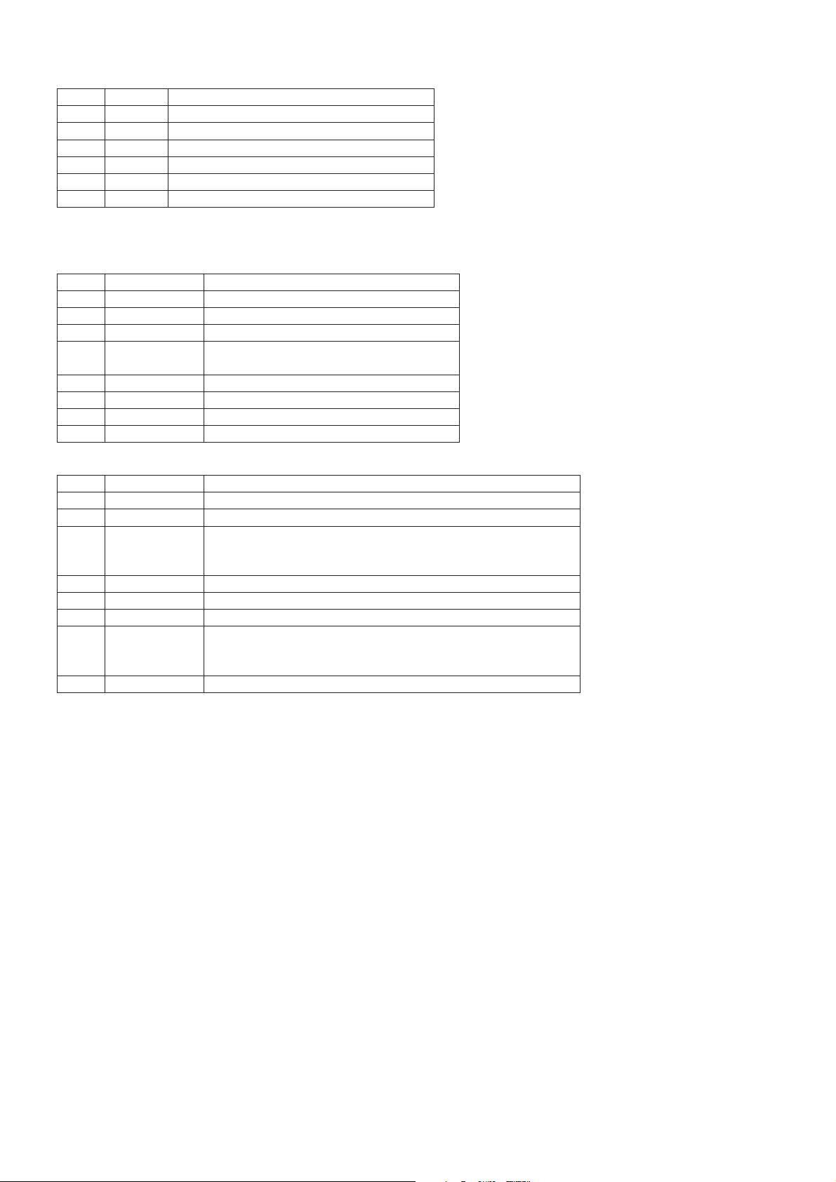
2 Precaution on handling of Optical pick-up (KMS-260B)
The laser diode in an optical pick-up is easy to be subject to electrostatic destruction. Therefore, solder-bridge the
laser tap on the flexible board when handling the optical pick-up.
When removing the flexible board from the connector, make a solder bridge in advance, then remove the board. Be
careful not to remove the solder bridge before inserting the connector. Moreover, take careful measures against
electrostatic destruction. The flexible board is cut easily. Handle the flexible board with care.
3 Precaution during adjustment
1) Perform the adjustment and confirmation marked with "O" in the order shown in the table when the parts below
are replaced.
Optical pick-up
IC6 D101 IC1, IC2, IC10
BD board
1.Temperature compensation offset adjustment X O O O
2. Laser power adjustment O O X O
3.Trtvense adjustment O O X O
4. Focus bias adjustment O O X O
5. Error rate confirmation O O X O
2) In the test mode, perform the adjustment. After adjustment is completed, chancel the test mode.
3) Perform the adjustment in the order described.
4) Use the following tools and measurement equipment.
CD test disc TGYS-1
Laser power meter
Oscilloscope (with bandwidth of more than 40 M Ohms)
(Calibrate the probe before measurement)
Digital voltmeter
Thermometer
5) Take care that VC and GND (ground) are not connected on the oscilloscope when two or more signals are monitored on the oscilloscope. (VC and GND are short-circuited in this case,)
4 Creating the recordable continuous recording disc
This disc is used for focus bias adjustment and error rate confirmation. How to create the recordable continuous
recording disc is 5-5
5 Offset Adjustment
No. Kay Display/Function
1 MULTI JOG Select [TEMP ADJUST]
2 PLAY [TEMP = xx (yy)]
(xx = compensation data, yy = setting temperature
3 MULTI JOG Input "yy" with present temp.
4 PL AY [TEMP=**SAVE]
[TEMP ADJUST] in writing data
5
Page 8
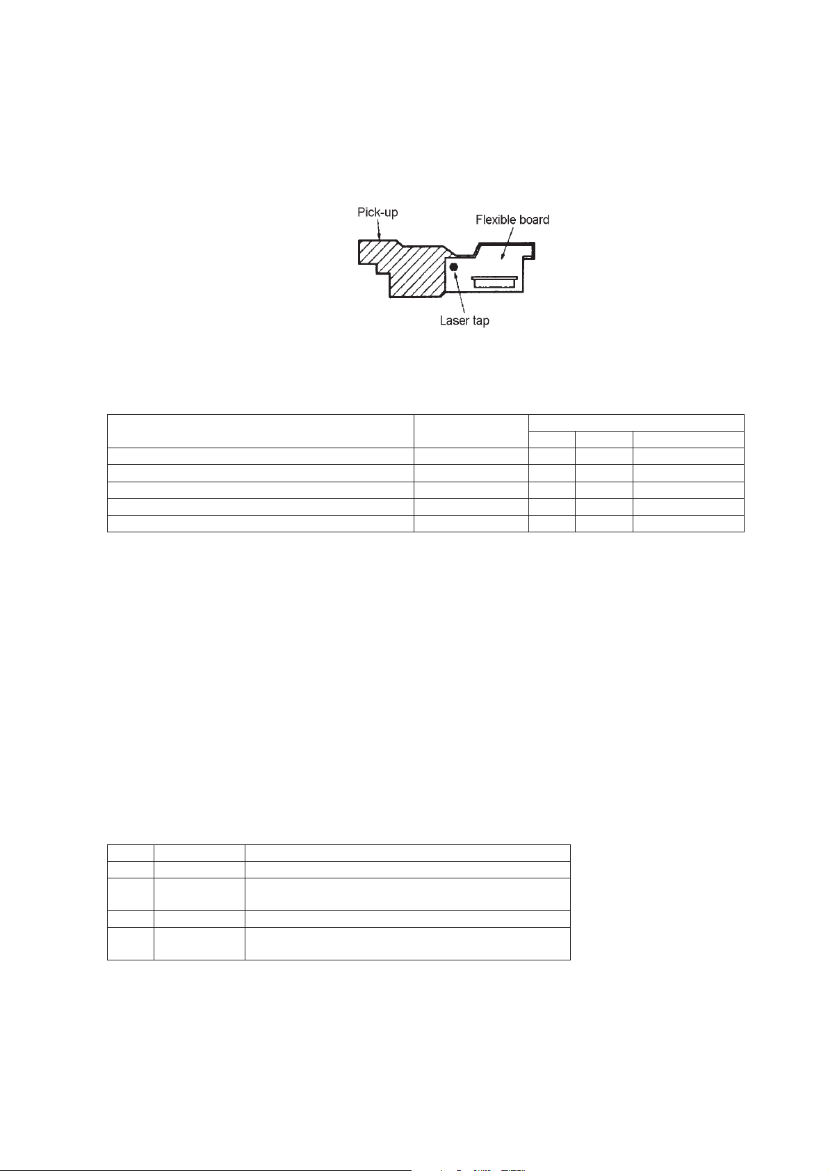
6 Laser Power Check and Adjustment
Laser power setting in playback and recording modes.
Preparation
1. Remove the MD mechanism from the unit
2. Remove the case and bracket.
3. Reconnect the flat cable of MD mechanism to the unit
1. Laser Power Adjustment
No. Key Display/Function
1 MULTI JOG [LDPWR ADJUST]
Load recordable disc
2 Load the disc and laser on [a0.9mW>$xx] read power
(xx = power value)
3 EJECT Unload the disc and laser on
4 FF/FB
(REC)
Move the pickup to check the laser power with laser power meter sensor
(Press the REC key if the pickup is In the proper position)
5 MULTI JOG Adjust “xx” so that the power meter shows 0.9mW.
6 PLAY [a7.0mW>$xx] writing power
7 UPIDOWN Adjust “xx” so that the power meter shows 7.0mW.
This adjustment should be carried out In 15secs.
8 PLAY Laser power off
Display shows [LDPWR ADJUST] after [LDPWR<$xx] to save the data In
E2PROM
Start from No.2 if readjust.
2. Laser Power Check
No. Key Display/Function
1 UP [LDPWR CHECK]
2 PL AY [c0.9mW>$xx]
(xx=0.85 to 0.95mW)
3 PL AY [c7.0mW>$xx]
Laser power meter: 7.0 + - 1.0mW*
7 Traverse Adjustment
V: 0.5V/div H: 10ms/div
INPUT: DC mode
6
Page 9
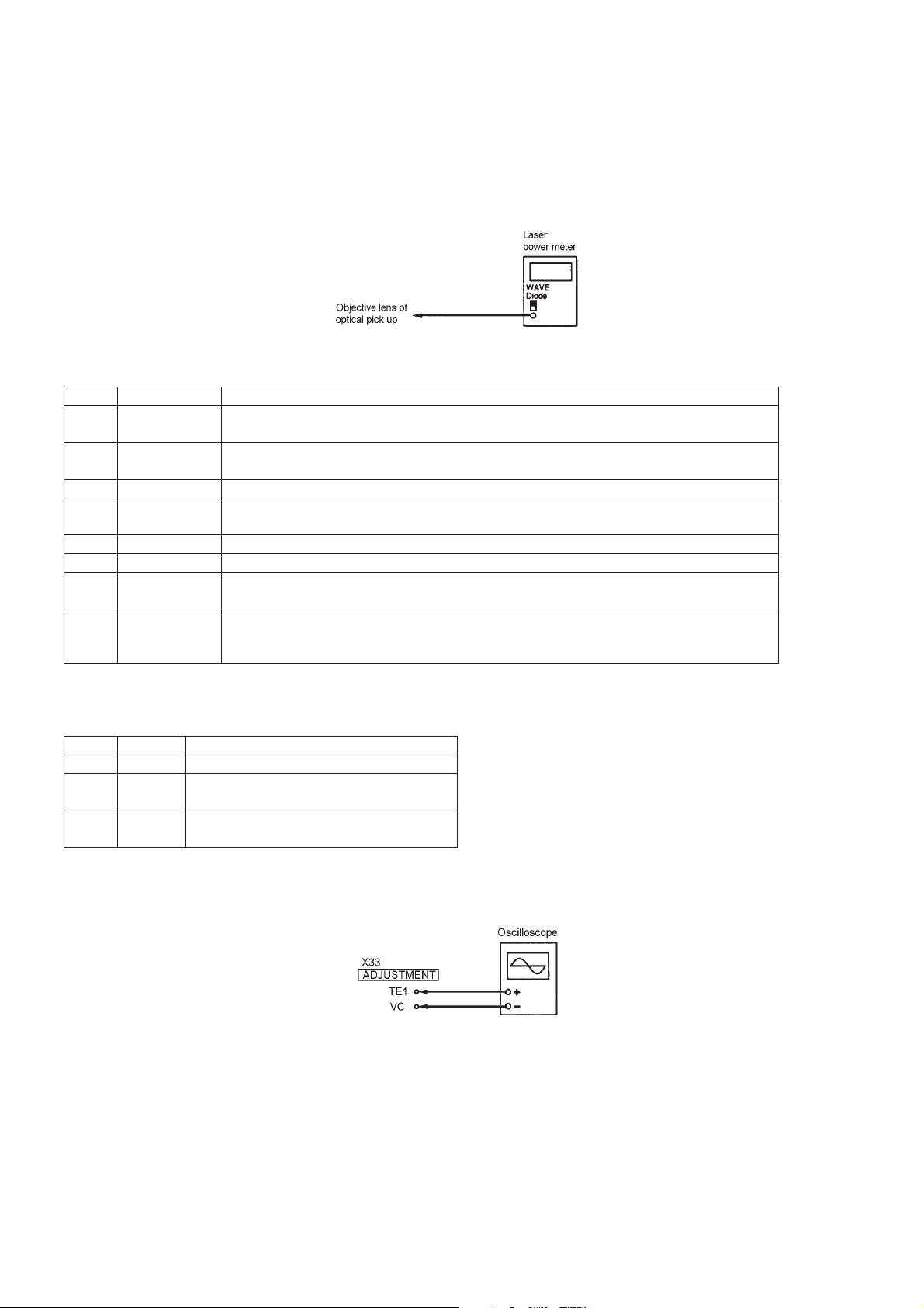
FE Balance
1. Recordable Disc
No. Key Display/Function
1 Connect the oscilloscope to TE1 and VC in X33 PCB
2 MULTI JOG Select [EFBAL ADJUST]
3 Load the recordable disc
4 PL AY [EFBAL MO-W]
5 PL AY [EF=$**MOW]
6 MULTI JOG Write adjustment. Adjust the waveform as follows.
7 PLAY Display shows [EF=$**MOR] after [EFB=**xSAVE] to save the data in
E2PROM.
Mode changes write to read
Focus and disc servo are on. Tracking servo off.
8 MULTI JOG Read power adjustment. Adjust the waveform as follows.
9 PL AY
PLAY
Save the data in E2PROM.
Display shows [EFBAL MO-P]
Display shows [EF=$**MOP]
(Pickup travels to search pits and tune the servo to on.)
10 MULTI JOG Adjust the waveform as follows.
11 PLAY Display shows [EFBAL CHANGE] after [EFB=**xSAVE] to save the data
in E2PROM.
Display shows [EFBAL CHANGE] disc motor stops.
12 EJECT Unload disc.
2. PER Master Test Disc (TGYS-1)
No. Key Display/Function
1 Load the disc (TGYS-1).
2 PLAY [EF=$**CD] servo is on
3 MULTI JOG Adjust the waveform as follows.
4 Save the data in E2PROM.
Display shows [EFB=**xSAVE] in brief time.
[EFBAL ADJUST]
5 EJ ECT Unload disc.
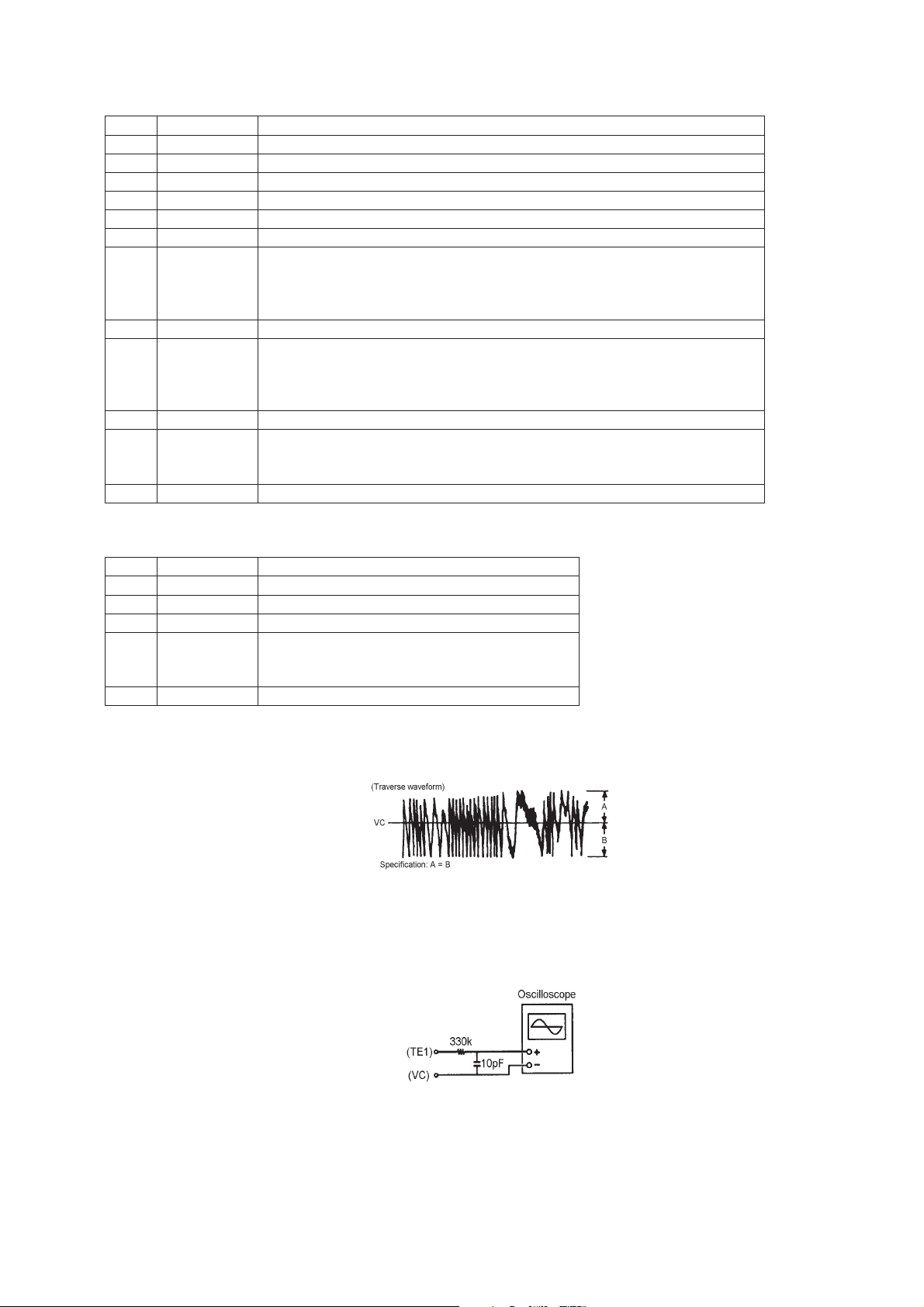
During this adjustment, the oscilloscope changes in units of about 2%. Adjust so that the waveform comes nearest to
the specified value. (MO groove read power traverse adjustment)
Notes:
1. Data is erased during MO write when a recorded disc is used for this adjustment
2. If the traverse waveform is difficult to be monitored, connect an oscilloscope as shown in the figure below.
7
Page 10

8 Focus Bias Adjustment
Use the special disc (continuous recorded disc)
No. Key Display/Function
1 MULTI JOG Select [FBIAS ADJUST]
2 Load the disc.
3 PLAY [a=xx yyyy/zz] point a
(xx = focus bias yyyy = C1error)
4 UP Adjust "yyyy" to 220*
5 PLAY [b=xx yyyy/zz] point b
6 DOWN Adjust "yyyy" to 220*
7 PLAY [xx yyyy/zzc=] point c
Check "yyyy" within 50
8 PLAY Display shows [aa bb cc(xx)] focus bias adjust
(aa = point a, bb=b, cc=c )
Notes:
1. The relation between the C1 error and focus bias value is shown in the figure below. Points "a" and "b" in the
figure are detected by the above adjustment. Focal position "C" is automatically obtained from points "a" and “b”
by calculation.
2. The C1 error rate fluctuates. Therefore, perform the adjustment according to the observed mean value.
9 Error Rate Check
1. CD Error Rate
No. Key Display/Function
1 MULTI JOG [CPLAY MODE]
2 Load the test disc (TGYS-1)
3 PLAY Display shows [CPLAY MID]
Access and
[c=xxxx a=yy] xxxx=C1 error (lower 20) yy = AIDP error
4 ST OP [CPLAY MODE]
5 EJ ECT Unload disc.
2. MO Error Rate
No. Key Display/Function
1 MULTI JOG [CPLAY MODE]
2 Load the recordable disc
3 PLAY Display shows [CPLAY MID]
Access and
[c=xxxx a=yy] xxxx=C1 error (lower 50) yy = AIDP error (00)
4 ST OP [CPLAY MODE]
5 EJ ECT Unload disc.
8
Page 11

3. WIRING DIAGRAM
9 10
Page 12

4. BLOCK DIAGRAM
11 12
Page 13

5. SCHEMATIC DIAGRAM
13 14
Page 14

6. PARTS LOCATION (Pattern Side)
REC BOARD
MAIN BOARD
IC12
Q20
IC9
IC8
Q10
Q12
IC7
Q8
Q9
IC11IC10
15 16
Page 15

MAIN BOARD
IC1
IC3
IC2
REC BOARD
Q2
Q1
Q14 Q15
IC4
Q21
Q4L
Q3L
Q4R
Q3R
Q19
Q16-Q18
Q5-Q7
IC13
17 18
Page 16

FRONT BOARD
Q302
Q303 - Q306
Q300
Q301
Q307
19 20
Page 17

7. IC DATA
IC1/3/4:NJM2068
Pin Configuration
IC7:TL431
Pin Assignment
Functional Block Diagram
REF
LP PACKAGE
(TOP VIEW)
CATHODE
V
ref
CATHODE
ANODE
REF
+
_
ANODE
21
Page 18

IC2:KIC9459N
PIN CONNECTION
PIN DESCRIPTION
22
Page 19

Outline 64P2G-A
out puts
out puts
55
54
53
52
51
50
49
48
47
46
45
44
43
42
39
36
10
11
12
13
14
15
16
17
18
19
20
21
22
23
24
25
27
29
30
31
32
41
40
38
37
35
34
64
63
62
61
59
57
56
XOUT
XIN
DIG12/SEG36
DIG13/SEG37
DIG14/SEG38
DIG15/SEG39
input
bidirectional ports
out puts
segment
out puts
PIN CONFIGURATION
RESET
SCK
SDATA
XIN ,
XOUT
P1, P0
Vcc1
Vcc2
Vss
Vp
Symbol
Pin name
Comment
Reset input
CS
Chip select
When "L", M66005 is initialized.
When "L", communication with the MCU is possible.
When "H", any instruction from the MCU is neglected.
Shift clock input
Serial input data is taken and shifted by the positive edge of SCK.
Serial data input
Clock input
Clock output
When use as a CR oscillator, connect external resistor and
capacitor.
When use an external clock, input external clock to XIN, and
XOUT must be opened.
DIG00~
DIG15
Digit output
Connect to digit (grid) pins of VFD.
Connect to segment (anode) pins of VFD. Pins from SEG00 to
SEG39 correspond to segment pins of VFD as shown in the table
below. SEG36~SEG39 pins are common to DIG12~DIG15 pins.
So, when use SEG36~SEG39, the number of digit to be used is
decreased.
Segment output
Universal port
Generally, use this port as the static output port.
This port also operates as the timing IN/OUT port to control
another M66005.
Positive power supply for internal logic.
Positive power supply for DIG and SEG outputs.
GND (0V)
Negative power supply to pull down.
SEG00~
SEG39
P1 : bidirectional
P0 : output
PIN DESCRIPTIONS
IC300:M66005F
1
DIG11
Digit /
2
DIG10
3
DIG09
4
DIG08
60
5
DIG07
Vcc2
SEG00
6
DIG06
Digit
SEG01
58
7
DIG05
SEG02
8
DIG04
SEG03
9
DIG03
SEG05
SEG04
DIG02
DIG01
SEG06
DIG00
SEG07
RESET
Reset input
SEG08
CS
Chip select input
SEG10
SEG09
SCK
SDATA
Serial data
Shift clock input
Segment
SEG12
SEG11
P1
P0
Universal
SEG13
Vcc1
SEG14
Clock output
SEG16
SEG15
Vss
Clock input
SEG17
SEG35
SEG18
SEG34
SEG19
SEG33
SEG20
26
SEG32
Segment
SEG21
SEG31
SEG22
28
SEG30
SEG23
SEG29
SEG24
SEG28
SEG25
SEG27
SEG26
33
Vp
input
23
Page 20

IC13:74HC04
PIN DESCRIPTION
PIN NO. SYMBOL NAME AND FUNCTION
1, 3, 5, 9, 11, 13 1A to 6A data inputs
2, 4, 6, 8, 10, 12 1Y to 6Y data outputs
7 GND ground (0 V)
14 V
CC
positive supply voltage
Fig.1 Pin configuration.
Fig.4 Functional diagram.
24
Fig.5 Schematic diagram
(one inverter).
Page 21

IC6:CXP84648
25 A_MUTE OUTPUT A_MUTE ACTIVE LOW O
26 D_MUTE OUTPUT D_MUTE ACTIVE LOW O
27 N.C I/O
28 PO_OFF_CONT OUTPUT FOR RLY ACTIVE HIGH O
29 BACKUP_V I
30 RESET INPUT CPU ACTIVE HIGH I
31 EXTAL OUTPUT FOR 12.288MHZ CRYSTAL O
32 XTAL 12.288MHZ CRYSTAL
33 VSS GND
34 32MHZ CRYSTAL
35 TEX OUTPUT FOR 32MHZ CRYSTAL O
36 AVSS AVSS GND
37 AVREF REFERENC VOLTAGE VDD
38 BACKUP_CH OUTPUT BACKUP CHACK O
39 KEY1 DATA INPUT KEY SCAN CHECK PORT for AD KEY INPUT O
40 KEY2 DATA INPUT KEY SCAN CHECK PORT for AD KEY INPUT O
41 KEY3 DATA INPUT KEY SCAN CHECK PORT for AD KEY INPUT O
42-45 N.C I/O
46 FL_RESET OUTPUT RESET FOR M66005 O
47 FL_CS OUTPUT CS FOR M66005 O
48-54 N.C I/O
55 RC5 SY IN/OUT SYSTEM CONTROL "HIGH": SYSTEM MODE, "LOW": INT MODE O
56 RMC OUTPUT FOR REMOCON DATA O
57-59 N.C O
60 PO_OFF_DET OUTPUT FOR POWER DOWN O
61 N.C I/O
62 N.C I/O
63 RC5_OUT OUTPUT FOR CONTROLING RC-5 O
64 RC5_IN INPUT FOR CONTROLING RC-5 I
65 FL_CLK OUTPUT CLK FOR M66005 O
66 N.C I/O
67 FL_DATA OUTPUT DATA FOR M66005 O
68 ENCODER I
69 ENCODER I
70 BACK/PO_ON OUTPUT TO DRIVE POWER ON(GREEN) ACTIVE HIGH O
71 ST-BY OUTPUT TO DRIVE STBY LED(RED) ACTIVE HIGH O
72 VDD VDD +5V
73 VDD VDD +5V
74 RMC-CONTROL OUTPUT FOR RC-5 ON/OFF O
75-80 N.C I/O
VSS
TX
PIN NO PIN NAME OPERATION DESCRIPTION ASSIGN
PIN ASSIGNMENT
PIN FUNCTION
PIN NO PIN NAME OPERATION DESCRIPTION ASSIGN
1-3 N.C I/O
4 ME_CTXD UART Communication O
5 ME_CRXD UART Communication I/O
6-13 N.C I/O
14 ME_BACK_ON O
15 CE O
16 M E_RESET O
17-19 N.C I/O
20 OPTION PULL-UP(ENG) / PUII-DOWN(JAP) I/O
21 N.C I/O
22 VOL_CLK CLK SIGNAL OUTPUT 9459F ELECTRONIC VOLUME CONTROL O
23 VOL_EN EN SIGNAL OUTPUT 9459F ELECTRONIC VOLUME CONTROL O
24 VOL_DA DA SIGNAL OUTPUT 9459F ELECTRONIC VOLUME CONTROL O
25 26
Page 22

8. EXPLODED VIEW AND PARTS LIST
49
E X2
H
A X2
E
B
2
E X2
46
45
L X4
12
K X7
11
K X2
10
8 X3
PD
9
F X2
23
7 X3
6 X3
5
22 X4
21 X3
20
24
M X2
25
26
K
13
K X2
A
27
14
A
A
A
48
18
47
16
15
A
28
D X4
A X4
38 X2
17
C X7
39 X2
4 X2
3
1
36
TL
29
30
TA X2
31
19
J X3
A1
35
34
H
33
32
PF
I
PC
37
44
43
42
41
40
G
27 28
Page 23

POS.
NO
VERS.
COLOR
PART NO.
(FOR PCS)
DESCRIPTION
PART NO.
(MJI)
POS.
NO
VERS.
COLOR
PART NO.
(FOR PCS)
DESCRIPTION
PART NO.
(MJI)
1 9965 000 11414 PANEL DOOR 325W162010
A nsp SCREW +2S 3x8
2 nsp LABEL LASER CAUTION-CD nsp
3 9965 000 10697 ARM DOOR L 323W002010
B nsp SCREW +2S 3x17
4 9965 000 10698 CUSHION DOOR 323W259010
A1 9965 000 11415 FRONT PANEL SUB ASSY 325W248500
5 nsp PANEL FRONT nsp
6 nsp BUTTON POWER B nsp
7 nsp BUTTON POWER A nsp
8 9965 000 11103 BUTTON DISPLAY 325W270040
9 9965 000 10701 DAMPER GEAR (KIFCO) 323W130010
10 9965 000 10702 BRACKET DOOR C 323W160060
11 nsp P.C.B ASSY FRONT nsp
12 nsp CHASSIS MAIN nsp
13 F nsp POWER TRANS
*TS001340R
100V/50HZ 57x27
13 N 9965 000 11416 POWER TRANS
*TS001330R
C nsp SCREW +2S 3x10
D nsp SCREW +3S 4x8
E nsp SCREW +2S 3x8
F nsp SCREW +2S 2x6 BK/PH nsp
G nsp SCREW +2S 3x8 PI9.5
H nsp SCREW +2S 3x5
I nsp SCREW +3S 3x5 BK/FH nsp
J nsp SCREW +2S 3x6
230V/50HZ 57x27
14 nsp BRACKET SIDE nsp
15 nsp SUPPORTER PCB nsp
16 F nsp CHASSIS BACK nsp
16 N nsp CHASSIS BACK nsp
17 F nsp STOPPER 323W259020
17 N 9965 000 11058 STOPPER 323W259030
18 F nsp MAINS CORD ASSY *YC000560R
18 N 9965 000 10705 MAINS CORD ASSY *YC000570R
K nsp SCREW +2S 3x8 ZNY/PH nsp
L nsp SCREW +3S 2.6x4 ZNW/BH nsp
M nsp SCREW 2PS 3x8Y nsp
PACKING
- N 9965 000 11419 USER GUIDE 325W851310
- F nsp USER GUIDE 325W851110
- N 9965 000 11420 REMOTE CONTROLLER
19 9965 000 11202 KNOB SHUTTLE 325W154010
20 9965 000 10708 BADGE MARANTZ 323W251010
- F nsp REMOTE CONTROLLER
21 9965 000 11109 BUTTON MENU 325W270010
22 9965 000 11110 BUTTON REC 325W270020
23 nsp WINDOW DISPLAY MD nsp
24 9965 000 11417 DOOR MD 325W162100
25 9965 000 11418 SPRING MD 325W115010
26 nsp BRACKET MD DOOR nsp
27 nsp SUPPORTER FLT MD nsp
28 nsp SUPPORTER P.C. nsp
29 9965 000 10709 WINDOW REMOCON B 323W158030
30 9965 000 10713 ARM DOOR R 323W002020
31 9965 000 11111 PLATE EARTH A 323W123010
32 9965 000 10714 SPRING DOOR C 323W115010
33 9965 000 10715 KNOB EJECT 323W154020
34 nsp SUPPORTER EJECT nsp
35 nsp WINDOW REMOCON A nsp
36 9965 000 10716 BRACKET DOOR A 323W160010
37 9965 000 10717 SPRING DOOR A 323W115020
38 9965 000 10718 CUSHION FOOT F 323W057010
39 9965 000 10719 CUSHION FOOT B 323W057020
40 9965 000 10720 HOLDER HINGE B 323W271020
41 9965 000 10721 HOLDER HINGE A 323W271010
42 9965 000 10703 SPRING DOOR B 323W115030
43 9965 000 10722 BRACKET DOOR B 323W160020
44 9965 000 10723 RING 323W353100
45 nsp BRACKET MECHA MD nsp
46 nsp MD MODULE MGM-07000A KPJ 325W304500
47 N nsp P.C.B ASSY MAIN nsp
47 F nsp P.C.B ASSY MAIN nsp
48 N nsp P.C.B ASSY REC nsp
48 F nsp P.C.B ASSY REC nsp
NOT STANDARD SPARE
49 9965 000 11113 CABINET TOP 324W257010
PC nsp PLATE EARTH "C" nsp
PF nsp PLATE EARTH "F" nsp
PD nsp PLATE EARTH "D" nsp
TA nsp TAPE ARM nsp
TL nsp TAPE LENS nsp
- N nsp CARD nsp
- F nsp CARD nsp
- F nsp CARD nsp
- nsp BOX,GIFT 325W801010
- nsp CUSHION,SNOW 323W809010
NOTE : "nsp" PART IS LISTED FOR REFERENCE ONLY, MARANTZ WILL NOT SUPPLY THESE PARTS.
29
B-TYPE ZNY/BH
nsp
nsp
B-TYPE ZNY/BH
nsp
B-TYPE(DOT) BK/BH
nsp
P+S-WASHER ZNY/BH
nsp
B-TYPE CR/BH
nsp
B-TYPE ZNY
nsp
B-TYPE BK/FH
nsp
B-TYPE ZNY/BH
ZK326W0010
RC110DRMD
ZK325W0010
RC110DRMDF
PARTS
Page 24

40
13
39
39
39
39
39
1
31
10
41
40
28
19
45
38
38
38
53
46
49
14
B
18
9
A
44
36
54
47
43
30
36
D
35
15
C
48
6
B
23
2
35
37
16
24
31
3
35
42
35
8
27
21
39
22
27
44
5
29
36
20
41
55
17
27
25
32
26
35
11
7
33
59
58
4
34
30
C
35
56
36
36
51
27
12
36
A
50
52
D
57
35
35
Page 25

POS.
NO
VERS.
COLOR
PART NO.
(FOR PCS)
DESCRIPTION
PART NO.
(MJI)
POS.
NO
VERS.
COLOR
PART NO.
(FOR PCS)
DESCRIPTION
PART NO.
(MJI)
1 nsp A10-3531 CHASSIS(TU) nsp
2 nsp J19-6125 BRACKET ASSY nsp
3 nsp G02-1716
nsp
FLAT SPRING(THRUST)
4 nsp D13-2510 RACK(GEAR) nsp
5 nsp D10-3958 LEVER(LIMIT) nsp
6 nsp A11-1189 SUB CHASSIS ASSY nsp
7 nsp D10-3959 ARM ASSY(MAIN) nsp
8 nsp D10-3961 LEVER ASSY(HEAD) nsp
9 nsp D10-3963 SLIDER(MAIN) nsp
10 nsp D13-2511 GEAR(FINAL) nsp
11 nsp J19-6127 HOLDER ASSY nsp
12 nsp A15-0106 FRAME nsp
13 nsp F11-0503 SHIELDING CASE nsp
15 nsp D10-3982 ROD(SUB) nsp
16 nsp D10-3957 ROD nsp
18 nsp A11-1187
nsp
SUB CHASSIS ASSY(TU)
19 nsp D13-2504 GEAR(LOAD A) nsp
20 nsp D13-2505 GEAR(LOAD B) nsp
21 nsp D13-2516 GEAR(LOAD C) nsp
24 nsp D13-2509 GEAR
nsp
(INTERMEDIATE)
25 nsp D10-3964 SLIDER(LOAD) nsp
26 nsp D10-3965 ARM(LOAD) nsp
27 nsp J02-1492 INSULATOR nsp
28 nsp G01-4230
nsp
TORSION COIL SP(SPM)
29 nsp G01-4231
nsp
EXTENSION COIL SPRING
30 nsp G01-4235
nsp
EXTENSION COIL SPRING
31 nsp G01-4233
nsp
TORSION COIL SPRING
32 nsp G01-4234
nsp
EXTENSION COIL SPRING
33 nsp N39-1745
nsp
MACHINE SCREW 1.7*4.5
34 nsp N09-3104
nsp
MECHINE SCREW 1.7*2
35 nsp N09-3279
nsp
MACHINE SCREW 1.7*3
36 nsp N09-5113
nsp
SCREW 1.7*7 (B-TITE)
37 nsp N09-5229 SCREW 1.4*1.8 nsp
38 nsp N09-5230
nsp
SCREW 1.4*2.2 (S-TITE)
39 nsp N09-5231
nsp
SCREW 1.7*4 (B-TITE)
40 nsp N86-2004
nsp
BIND TAPTITE SC 2*4(S-TITE)
41 nsp N19-0366
nsp
FLAT WASHER 2.1*4*0.5CUT
42 nsp N19-1511
nsp
FLAT WS 2.5*0.9*0.25 CUT
43 nsp N19-1171
nsp
FLAT WS 1.6*3.5*0.25 CUT
44 nsp N09-5285
nsp
MACHINE SCREW(B) 1.7*4.5
45 nsp T42-0983 MOTOR ASSY *MM001170R
47 nsp E35-2689
nsp
WIRING HARNESS(SLED)
49 nsp E35-2690 WIRE HARNESS nsp
50 nsp E35-2691 FLAT CABLE L=80MM *YU000960R
51 nsp E35-2348 FLAT CABLE(PU) 21P *YU000970R
52 nsp X33-1260 PCB ASSY *ZZ001870R
53 nsp T42-0984 MOTOR ASSY(LOAD) *MM001180R
54 nsp T42-0985 MOTOR ASSY(SLED) *MM001190R
55 nsp D13-2506 GEAR ASSY nsp
56 nsp G16-1236 SHEET nsp
57 nsp G11-2825 SOFT TAPE nsp
58 nsp T25-0111-05 PICKUP KMS-260E *ZZ001880R
59 nsp T30-0027-05
*LH400180R
REC HEAD RM-21E
NOTE : "nsp" PART IS LISTED FOR REFERENCE ONLY, MARANTZ WILL NOT SUPPLY THESE PARTS.
31
Page 26

9. ELECTRICAL PARTS LIST
ASSIGNMENT OF COMMON PARTS CODES.
RESISTORS
R : 1) GD05 × × × 140, Carbon film fixed resistor, ±5% 1/4W
R : 2) GD05 × × × 160, Carbon film fixed resistor, ±5% 1/6W
Examples ;
Resistance value
➀
0.1 Ω .... 001 10 Ω .... 100 1 kΩ .... 102 100 kΩ .... 104
0.5 Ω .... 005 18 Ω .... 180 2.7 kΩ .... 272 680 kΩ .... 684
1 Ω .... 010 100 Ω .... 101 10 kΩ .... 103 1 MΩ .... 105
6.8 Ω .... 068 390 Ω .... 391 22 kΩ .... 223 4.7 MΩ .... 475
Note : Please distinguish 1/4W from 1/6W by the shape of parts
used actually.
CAPACITORS
C : CERAMIC CAP.
3) DD1 × × × × 370, Ceramic capacitor
Examples ;
Tolerance (Capacity deviation)
➁
±0.25 pF .... 0
Tolerance of COMMON PARTS handled here are as follows :
C : CERAMIC CAP.
Examples ;
C : 5) ELECTROLY CAP. ( ), 6) FILM CAP. ( )
Examples ;
0.5 pF 5 pF .... ±0.25 pF
Capacity value
➂
0.5 pF ....005 3 pF .... 030 100 pF .... 101
1.5 pF ....015 47 pF .... 470 560 pF .... 561
4) DK16 × × × 300, High dielectric constant ceramic
Capacity value
➃
100 pF .... 101 1000 pF .... 102 10000 pF ....103
470 pF .... 471 2200 pF .... 222
5) EA × × × × × × 10, Electrolytic capacitor
Capacity value
➄
0.1 µF.... 104 4.7 µF .... 475 100 µF ....107
0.33 µF.... 334 10 µF .... 106 330 µF ....337
Working voltage
➅
{
➂
{
{
➅
Resistance value
Disc type
Temp.coeff.P350 N1000, 50V
Capacity value
Tolerance
capacitor
Disc type
Temp.chara. 2B4, 50V
Capacity value
One-way lead type, Tolerance ±20%
Working voltage
Capacity value
2200 µF ....228
➀
{
➁
±0.5 pF .... 1
±5% .... 5
6 pF 10 pF .... ±0.5 pF
12 pF 560 pF .... ±5%
1 pF .... 010 10 pF .... 100 220 pF .... 221
➃
{
➄
1 µF....105 22 µF .... 226 1100 µF....118
6.3V.... 006 25V .... 025
10V .... 010 35V ....035
16V .... 016 50V ....050
NOTE ON SAFETY FOR FUSIBLE RESISTOR :
The suppliers and their type numbers of fusible resistors
are as follows;
1. KOA Corporation
Part No. (MJI) Type No. (KOA) Description
NH05 × × × 140 RF25S × × × × ΩJ(±5% 1/4W)
NH05 × × × 120 RF50S × × × × ΩJ(±5% 1/2W)
NH85 × × × 110 RF73B2A × × × × ΩJ(±5% 1/10W)
NH95 × × × 140 RF73B2E × × × × ΩJ(±5% 1/4W)
2. Matsushita Electronic Components Co., Ltd
Part No. (MJI) Type No. (MEC) Description
NF05 × × × 140 ERD-2FCJ × × × (±5% 1/4W)
RF05 × × × 140
NF02 × × × 140
RF02 × × × 140
Examples ;
{
Resistance value
ERD-2FCG
{
Resistance value
Resistance value
0.1 Ω .... 001 10 Ω .... 100 1 kΩ .... 102 100 kΩ .... 104
0.5 Ω .... 005 18 Ω .... 180 2.7 kΩ .... 272 680 kΩ .... 684
1 Ω .... 010 100 Ω .... 101 10 kΩ .... 103 1 MΩ .... 105
6.8 Ω .... 068 390 Ω .... 391 22 kΩ .... 223 4.7 MΩ .... 475
{
Resistance value
(0.1 Ω − 10 kΩ)
× × × (±2% 1/4W)
{
Resistance value
ABBREVIATION AND MARKS
ANT. : ANTENNA BATT. : BATTERY
CAP. : CAPACITOR CER. : CERAMIC
CONN. : CONNECTING DIG. : DIGITAL
HP : HEADPHONE MIC. : MICROPHONE
µ-PRO : MICROPROCESSOR REC. : RECORDING
RES. : RESISTOR SPK : SPEAKER
SW : SWITCH TRANSF. : TRANSFORMER
TRIM. : TRIMMING TRS. : TRANSISTOR
VAR. : VARIABLE X’TAL : CRYSTAL
NOTE ON FUSE :
Regarding to all parts of parts code FS20xxx2xx, replace
only with Wickmann-Werke GmbH, Type 372 non glass type
fuse.
6) DF15 × × × 350 Plastic film capacitor
DF15 × × × 310 One-way type, Mylar ±5% 50V
DF16 × × × 310 Plastic film capacitor
Examples ;
Capacity value
➆
0.001 µF (1000 pF) ....... 102 0.1 µF.... 104
0.0018 µF ........................ 182 0.56 µF.... 564
0.01 µF........................ 103 1 µF.... 105
0.015 µF ........................ 153
: 1) The above CODES ( R , R , C , C and
NOTE
C ) are omitted on the schematic diagram in some
case.
2) On the occasion, be confirmed the common parts on
the parts list.
3) Refer to “Common Parts List” for the other common
parts (RI05, DD4, DK4).
➆
{
One-way type, Mylar ±10% 50V
Capacity value
NOTE ON SAFETY :
Symbol Fire or electrical shock hazard. Only original
parts should be used to replaced any part marked with
symbol . Any other component substitution (other
than original type), may increase risk of fire or electrical
shock hazard.
010728MIT
32
Page 27

VERS.
POS.
COLOR
NO
C6L
C6R
C7L
C7R
C8L
C8R
C9L
C9R
C10L
C10R
C11
C12
C13
C14
C15
C16
C17
C18
9965 000 11120 CER.AC(SAFETY),
PART NO.
(FOR PCS)
DESCRIPTION
MAIN CIRCUIT BOARD
MAIN - CAPACITORS
nsp ELECT,22µF-M/16V,5x5-5RE nsp
nsp ELECT,22µF-M/16V,5x5-5RE nsp
nsp FILM,ST-0.0027µF-J/100V-5RE nsp
nsp FILM,ST-0.0027µF-J/100V-5RE nsp
nsp CER.CHIP,220pF-J/50V-1608 nsp
nsp CER.CHIP,220pF-J/50V-1608 nsp
nsp ELECT,22µF-M/16V,5x5-5RE nsp
nsp ELECT,22µF-M/16V,5x5-5RE nsp
nsp CER.CHIP,470pF-J/50V-1608 nsp
nsp CER.CHIP,470pF-J/50V-1608 nsp
nsp CER.CHIP,0.01µF-K/50V-1608 nsp
nsp CER.CHIP,10pF-D/50V-1608 nsp
nsp CER.CHIP,0.1µF-K/50V-1608 nsp
nsp CER.CHIP,22pF-J/50V-1608 nsp
nsp CER.CHIP,0.1µF-K/50V-1608 nsp
nsp CER.CHIP,0.1µF-K/50V-1608 nsp
nsp CER.CHIP,22pF-J/50V-1608 nsp
DE7150-487F 472MVAI
C19
C20
nsp CER.,0.01µF-Z/500V-5RE nsp
nsp ELECT,1000µF-M/25V(SHL),
10x20L-5RE OEMONLY
C21
C22
nsp ELECT,SHL 10000µF 16V M
nsp CER.CHIP,0.01µF-K/50V-1608 nsp
18x35 P=7.5MM
C23
nsp CER.,0.01µF-Z/500V-5RE nsp
C28
C29
C30
C31
C32
C33
C34
C35
C36
C37
C38
C39
C40
C41
C42
9965 000 11128 DOUBLE LAYER(70),
nsp CER.CHIP,0.01µF-K/50V-1608 nsp
nsp CER.CHIP,100pF-J/50V-1608 nsp
nsp ELECT,10µF-M/50V,5x11-5RE nsp
nsp ELECT,100µF-M/50V,8x11.5-5 nsp
nsp ELECT,10µF-M/50V,5x11-5RE nsp
nsp ELECT,2200µF-M/16V,10x20 nsp
nsp ELECT,2200µF-M/16V,10x20 nsp
nsp CER.CHIP,0.01µF-K/50V-1608 nsp
nsp CER.CHIP,27pF-J/50V-1608 nsp
nsp ELECT,470µF-M/10V,6.3x11-5 nsp
nsp CER.CHIP,100pF-J/50V-1608 nsp
nsp ELECT,1000µF-M/10V,10x12.5 nsp
nsp CER.CHIP,0.1µF-K/50V-1608 nsp
0.047F-70UA/5.5V-5RE
C43
C44
C45
C46
C47
C48
9965 000 11120 CER.AC(SAFETY),DE7150-487F
nsp CER.CHIP,0.1µF-K/50V-1608 nsp
nsp CER.CHIP,220pF-J/50V-1608 nsp
nsp CER.CHIP,220pF-J/50V-1608 nsp
nsp ELECT,1µF-M/50V,3x5-5RE nsp
nsp CER.CHIP,0.1µF-K/50V-1608 nsp
472MVAI
C49
C50
9965 000 11120 CER.AC(SAFETY),
nsp ELECT,10µF-M/50V,5x11-5RE nsp
DE7150-487F 472MVAI
C51
C52
C53
9965 000 11128 DOUBLE LAYER(70),
nsp CER.CHIP,27pF-J/50V-1608 nsp
nsp ELECT,2.2µF-M/50V,5x11-5RE nsp
0.047F-70UA/5.5V-5RE
C55
C56
C57
C58
R10
R11
nsp ELECT,47µF-M/16V,5x11-5RE nsp
nsp CER.CHIP,0.1µF-K/50V-1608 nsp
nsp CER.CHIP,18pF-J/50V-1608 nsp
nsp CER.CHIP,18pF-J/50V-1608 nsp
MAIN - RESISTORS
nsp CHIP,3.3K-J,1/16W-1608REEL nsp
nsp CHIP,3.3K-J,1/16W-1608REEL nsp
PART NO.
(MJI)
DK17472840
nsp
nsp
*EX000090R
DK17472840
DK17472840
*EX000090R
POS.
NO
R12
R13L
R13R
R14L
R14R
R15L
R15R
R16L
R16R
R17L
R17R
R18L
R18R
R19L
R19R
R20L
R20R
R21
R22
R23
R24
R25
R26
R27
R28
R29
R30
R31
R32
R33
R34
R37
R38
R39
R40
R41
R42
R43
R44
R45
R46
R47
R48
R49
R50
R51
R52
VERS.
COLOR
N
F
PART NO.
(FOR PCS)
DESCRIPTION
nsp CHIP,680-J,1/16W-1608REEL nsp
nsp CHIP,4.7K-J,1/16W-1608REEL nsp
nsp CHIP,4.7K-J,1/16W-1608REEL nsp
nsp CHIP,12K-J,1/16W-1608REEL nsp
nsp CHIP,12K-J,1/16W-1608REEL nsp
nsp CHIP,4.7K-J,1/16W-1608REEL nsp
nsp CHIP,4.7K-J,1/16W-1608REEL nsp
nsp CHIP,220-J,1/16W-1608REEL nsp
nsp CHIP,220-J,1/16W-1608REEL nsp
nsp CHIP,220-J,1/16W-1608REEL nsp
nsp CHIP,220-J,1/16W-1608REEL nsp
nsp CHIP,100-J,1/16W-1608REEL nsp
nsp CHIP,100-J,1/16W-1608REEL nsp
nsp CHIP,4.7K-J,1/16W-1608REEL nsp
nsp CHIP,4.7K-J,1/16W-1608REEL nsp
nsp CHIP,4.7K-J,1/16W-1608REEL nsp
nsp CHIP,4.7K-J,1/16W-1608REEL nsp
nsp CHIP,100K-J,1/16W-1608REEL nsp
nsp CHIP,100-J,1/16W-1608REEL nsp
nsp CHIP,75-J,1/16W-1608REEL nsp
nsp CHIP,100K-J,1/16W-1608REEL nsp
nsp CHIP,10K-J,1/16W-1608REEL nsp
nsp CHIP,2.2K-J,1/16W-1608REEL nsp
nsp CHIP,120-J,1/16W-1608REEL nsp
nsp CHIP,120-J,1/16W-1608REEL nsp
nsp 47-J,1/4W-R.REEL nsp
nsp 4.7-J,1/4W,R.REEL nsp
nsp CHIP,2.2K-J,1/16W-1608REEL nsp
nsp 5.6K-J,1/5W-52RE-AX nsp
nsp 22K-J,1/5W-52RE-AX nsp
nsp CHIP,10K-J,1/16W-1608REEL nsp
nsp 150-J,1W-R.REEL nsp
nsp 1.6K-J,1/5W-52RE-AX nsp
nsp 1.5K-J,1/5W-52RE-AX nsp
nsp 4.7K-J,1/5W-52RE-AX nsp
nsp CHIP,100-J,1/16W-1608REEL nsp
nsp CHIP,100K-J,1/16W-1608REEL nsp
nsp CHIP,4.7K-J,1/16W-1608REEL nsp
nsp CHIP,47K-J,1/16W-1608REEL nsp
nsp CHIP,47K-J,1/16W-1608REEL nsp
nsp CHIP,3.9K-J,1/16W-1608REEL nsp
nsp CHIP,1K-J,1/16W-1608REEL nsp
nsp CHIP,2.7K-J,1/16W-1608REEL nsp
nsp CHIP,100K-J,1/16W-1608REEL nsp
nsp CHIP,100K-J,1/16W-1608REEL nsp
nsp CHIP,100-J,1/16W-1608REEL nsp
nsp CHIP,10K-J,1/16W-1608REEL nsp
R57
R58
R59
R60
R65
R66
R67
R68
R69
R70
R71L
R71R
R73
R74
R75
R77
nsp CHIP,12K-J,1/16W-1608REEL nsp
nsp CHIP,12K-J,1/16W-1608REEL nsp
nsp CHIP,12K-J,1/16W-1608REEL nsp
nsp CHIP,47-J,1/16W-1608REEL nsp
nsp CHIP,1K-J,1/16W-1608REEL nsp
nsp CHIP,47-J,1/16W-1608REEL nsp
nsp CHIP,1K-J,1/16W-1608REEL nsp
nsp CHIP,1M-J,1/16W-1608REEL nsp
nsp CHIP,10K-J,1/16W-1608REEL nsp
nsp CHIP,680-J,1/16W-1608REEL nsp
nsp CHIP,680-J,1/16W-1608REEL nsp
nsp 1-J,1/4W-R.TYPE REEL nsp
nsp CHIP,47K-J,1/16W-1608REEL nsp
nsp CHIP,2.2K-J,1/16W-1608REEL nsp
nsp 1-J,1/4W-R.TYPE REEL nsp
PART NO.
(MJI)
NOTE : "nsp" PART IS LISTED FOR REFERENCE ONLY, MARANTZ WILL NOT SUPPLY THESE PARTS.
33
Page 28

VERS.
POS.
COLOR
NO
MAIN - SEMICONDUCTORS
D1
9965 000 11119 D CHIP,1SS355USM *HD201580R
D5
D6
9965 000 10728 DIODE,IN4007 52 1000V 1A *HD201570R
D9
D11
4822 130 32778 DIODE,1SS133T-72-52MM HD20015210
D12
4822 130 83067 D,RECTIFIER BRIDGE,
D13
9965 000 10728 DIODE,IN4007 52 1000V 1A *HD201570R
D20
D23
9965 000 11119 D CHIP,1SS355USM *HD201580R
D24
9965 000 11119 D CHIP,1SS355USM *HD201580R
D27
9965 000 11119 D CHIP,1SS355USM *HD201580R
D28
4822 130 32778 DIODE,1SS133T-72-52MM HD20015210
D29
4822 130 32778 DIODE,1SS133T-72-52MM HD20015210
D30
9965 000 11119 D CHIP,1SS355USM *HD201580R
D31
9965 000 11119 D CHIP,1SS355USM *HD201580R
D32
9965 000 11119 D CHIP,1SS355USM *HD201580R
IC4
5322 209 13406 IC,NJM2068MD-SOP8P *HC107380R
IC7
4822 209 81397 ILINEAR-REGULATOR,
IC8
4822 209 31631 IC,KIA7805PI,
IC9
4822 209 31631 IC,KIA7805PI,
PART NO.
(FOR PCS)
DESCRIPTION
D3SB20/DBF40C 5A-4PIN
TL431CLP 3PIN
20W-TO220IS MOLD
PART NO.
(MJI)
HE20020290
*HC300440R
HC3890509F
HC3890509F
POS.
NO
Q18
Q18
Q18
Q19
Q20
Q21
ZD1
ZD2
ZD3
ZD4
ZD5
CN1
CN2
CN3
20W-TO220IS MOLD
IC10
9965 000 11426 IC,ICP-N15
FU60115020
CN4
T104/PROTEC-REEL
IC11
9965 000 11426 IC,ICP-N15
FU60115020
CN5
T104/PROTEC-REEL
IC12
9965 000 11129 IC,KIA7032P,3.2V/TO92-RELL *HC107390R
IC13
9965 000 10992 IC,INVRTR
MC74HCU04AD SOP14
Q1
9965 000 11427 CHIP TRS.2SA,KRA103S (SOP) *BA001400R
Q2
4822 130 60729 CHIP TRS.2SC,
DTC124EK,0.2W/SMT-REEL
Q3L
9965 000 10744 CHIP TRS.2SC,
KTC2875B 0.15W/LOW-ON-RES
*HC700180R
*BA001080R
*HT300870R
F1
F1
F1L
F1R
GND1
SOT23(RTK)-REEL
Q3R
9965 000 10744 CHIP TRS.2SC,
KTC2875B 0.15W/LOW-ON-RES
SOT23(RTK)-REEL
Q4L
9965 000 10744 CHIP TRS.2SC,
KTC2875B 0.15W/LOW-ON-RES
SOT23(RTK)-REEL
Q4R
9965 000 10744 CHIP TRS.2SC,
KTC2875B 0.15W/LOW-ON-RES
SOT23(RTK)-REEL
Q5
4822 130 60729 CHIP TRS.2SC,
DTC124EK,0.2W/SMT-REEL
Q6
4822 130 60729 CHIP TRS.2SC,
DTC124EK,0.2W/SMT-REEL
Q7
9965 000 11427 CHIP TRS.2SA,KRA103S (SOP) *BA001400R
Q8
4822 130 50437 SEMI,BRT/NPN RC,DTC143ES,
0.3W/TO92M-REEL
Q9
9965 000 10444 SEMI,BRT/NPN RC,KRC107M,
0.4W/TO92M-REEL
Q10
4822 130 11683 SEMI,TR/GE PNP 2SA,
KSA916Y,0.9W/TO92L-REEL
Q12
9965 000 11425 SEMI,TR/GE NPN 2SD,
KTC2026Y TO220IS BULK 2W
Q14
4822 130 60326 CHIP TRS.2SA,
DTA144EK,0.2W/SMT-REEL
Q15
4822 130 60729 CHIP TRS.2SC,
DTC144EK,0.2W/SMT-REEL
Q18
N 9965 000 10753 CHIP TRS.2SC,
*HT300870R
*HT300870R
*HT300870R
*BA001080R
*BA001080R
*BA001300R
*BA001070R
*HT100460R
*HT300780R
*BA001050R
*BA001040R
*BA001220R
J8
J126
JACK1
JACK2
JACK3
JACK4
LT1
RL1
SW1
T1
T1
W1
W2
XTAL1
XTAL2
KRC102S T/P (KEC)
NOTE : "nsp" PART IS LISTED FOR REFERENCE ONLY, MARANTZ WILL NOT SUPPLY THESE PARTS.
34
VERS.
COLOR
N 4822 130 60729 CHIP TRS.2SC,
PART NO.
(FOR PCS)
DESCRIPTION
PART NO.
(MJI)
*BA001040R
DTC144EK,0.2W/SMT-REEL
F 9965 000 10753 CHIP TRS.2SC,
*BA001220R
KRC102S T/P (KEC)
F 4822 130 60729 CHIP TRS.2SC,
*BA001040R
DTC144EK,0.2W/SMT-REEL
9965 000 10753 CHIP TRS.2SC,
*BA001220R
KRC102S T/P (KEC)
4822 130 61227 SEMI,BRT/PNP RA,
*BA001330R
DTA114ES,0.3W/TO92M-REEL
4822 130 90326 CHIP TRS.2SA,
*BA001280R
DTA114TK,0.2W/SMT-REEL
9965 000 11210 D,ZENER,MTZJ20B-0.5W/
*HD301950R
5MA-52MM
4822 130 11627 D,ZENER,MTZJ15B-0.5W/
*HD302000R
5MA-52MM
4822 130 11627 D,ZENER,MTZJ15B-0.5W/
*HD302000R
5MA-52MM
4822 130 10667 D,ZENER,MTZJ4.7B-0.5W/
HD30471000
5MA-52MM
4822 130 80317 D,ZENER,MTZJ5.1B-0.5W/
HD30511000
5MA-52MM
MAIN - MISCELLANEOUS
nsp CN.FPC 1.0MM,
nsp
52806-2610 26P STRAIGHT
nsp CN.WAFER 2.5MM,5267-08A 8P nsp
nsp CN.FPC 1.0MM,
nsp
52806-1910 19P STRAIGHT
nsp CN.WAFER 2.0MM,
nsp
35336-1010 10P
nsp CN.WAFER 2.0MM,
nsp
35336-0510 5P
N 4822 070 31601 FUSE (5.2x20),
*FS000450R
250V-T160MA-S/V/B/R(YARN)
F
nsp FUSE (5.2x20),250V-S1A-U/ *FS000830R
nsp HOLDER,FUSE CLIP,
nsp
PI5.2-REEL
nsp HOLDER,FUSE CLIP,
nsp
PI5.2-REEL
nsp TERMINAL,
nsp
ALL PBST/GND PLATE-REEL
nsp CHIP,0-J,1/8W-3216REEL nsp
9965 000 10734 TER,RCA 4PIN,
*YT002460R
DAERYUNG/JK040131PN
9965 000 11212 MODULE,GP1F37R1/
*YJ002500R
OPTICAL TRANSMITE
9965 000 11127 TER,RCA 1PIN,
*YT002670R
JE010003PN(GND) BLACK
9965 000 11126 TER,RCA 2PIN,JK020130LN
*YJ002490R
(GND PLATE&PIN)/ORINGE
9965 000 11422 COIL,LINE FILTER,
*FN000150R
UU1116 1MH(411B)
9965 000 11424 RELAY,SDT-S-109LMR
*LY000280R
9V 250V/5A
9965 000 10732 SW,SLIDE,SSAF112NA011 *SS000700R
N 9965 000 11027 TRANS ST/BY,230/50 RV5080R
*TS001540R
28x25 Io=22MA 12.5Vx0.1A(DC)
F
nsp TRANS ST/BY,AVC5/
*TS001370R
100V 50HZ 28x15
nsp CN.WAFER 7.92MM,
nsp
YW396-32V 2P
nsp CN.WAFER 3.96MM,35328-0210 nsp
9965 000 11423 CRYSTAL,12.288MHZ,
*JX000890R
HC49U-CL;20pF
9965 000 11124 CRYSTAL,MX-38T(32.768KHZ)
*JX000830R
NDK
Page 29

VERS.
POS.
COLOR
NO
FRONT CIRCUIT BOARD
FRONT - CAPACITORS
C300
C301
nsp CER.CHIP,0.01µF-K/50V-1608 nsp
C304
C305
C306
C308
C309
nsp CER.CHIP,0.1µF-K/50V-1608 nsp
C312
C313
C314
C315
C316
C317
R300
R301
R302
R303
R304
R305
R306
R307
R308
R309
R310
R311
R312
R313
R314
R315
R316
R317
R318
R319
R320
R321
R322
R323
R324
R327
R328
R329
FRONT - SEMICONDUCTORS
D300
9965 000 11119 D CHIP,1SS355USM *HD201580R
D301
9965 000 11119 D CHIP,1SS355USM *HD201580R
IC300
9965 000 10762 IC,M66005FP-SOP64P /
Q300
9965 000 10753 CHIP TRS.2SC,KRC102S T/P
Q301
9965 000 10753 CHIP TRS.2SC,KRC102S T/P
Q302
9965 000 10753 CHIP TRS.2SC,KRC102S T/P
Q303
4822 130 60941 CHIP TRS.2SA,DTA114EK,
Q304
9965 000 11131 CHIP TRS.2SC,KRC104S (SOP) *BA001290R
Q305
4822 130 60941 CHIP TRS.2SA,DTA114EK,
Q306
9965 000 11131 CHIP TRS.2SC,KRC104S (SOP) *BA001290R
Q307
9965 000 10753 CHIP TRS.2SC,KRC102S T/P
NOTE : "nsp" PART IS LISTED FOR REFERENCE ONLY, MARANTZ WILL NOT SUPPLY THESE PARTS.
PART NO.
(FOR PCS)
DESCRIPTION
PART NO.
(MJI)
POS.
NO
ZD300
nsp ELECT,100µF-M/10V,6.3x5-5RE nsp
CP3
nsp CER.CHIP,0.1µF-K/50V-1608 nsp
nsp CER.CHIP,100pF-J/50V-1608 nsp
nsp ELECT,100µF-M/10V,6.3x5-5RE nsp
nsp CER.CHIP,220pF-J/50V-1608 nsp
nsp CER.CHIP,220pF-J/50V-1608 nsp
nsp CER.CHIP,220pF-J/50V-1608 nsp
nsp CER.CHIP,0.047µF-Z/50V-1608 nsp
nsp CER.CHIP,0.047µF-Z/50V-1608 nsp
FRONT - RESISTORS
nsp CHIP,1.5K-J,1/16W-1608REEL nsp
nsp CHIP,1.8K-J,1/16W-1608REEL nsp
nsp CHIP,2.2K-J,1/16W-1608REEL nsp
nsp CHIP,2.7K-J,1/16W-1608REEL nsp
FLT300
LED300
LED301
LED302
RM300
SW300
SW301
SW307
SW308
SW309
SW310
nsp CHIP,1.5K-J,1/16W-1608REEL nsp
nsp CHIP,1.8K-J,1/16W-1608REEL nsp
SW311
nsp CHIP,2.2K-J,1/16W-1608REEL nsp
nsp CHIP,1.5K-J,1/16W-1608REEL nsp
SW311
nsp CHIP,1.8K-J,1/16W-1608REEL nsp
nsp CHIP,2.2K-J,1/16W-1608REEL nsp
nsp CHIP,2.7K-J,1/16W-1608REEL nsp
nsp CHIP,47-J,1/16W-1608REEL nsp
nsp CHIP,270-J,1/16W-1608REEL nsp
nsp CHIP,270-J,1/16W-1608REEL nsp
nsp CHIP,270-J,1/16W-1608REEL nsp
nsp CHIP,1K-J,1/16W-1608REEL nsp
nsp CHIP,100-J,1/16W-1608REEL nsp
nsp CHIP,100-J,1/16W-1608REEL nsp
nsp CHIP,10K-J,1/16W-1608REEL nsp
nsp CHIP,27K-J,1/16W-1608REEL nsp
nsp CHIP,4.7K-J,1/16W-1608REEL nsp
nsp CHIP,4.7K-J,1/16W-1608REEL nsp
nsp CHIP,270-J,1/16W-1608REEL nsp
nsp CHIP,4.7K-J,1/16W-1608REEL nsp
nsp CHIP,1K-J,1/16W-1608REEL nsp
nsp CHIP,1K-J,1/16W-1608REEL nsp
nsp CHIP,1K-J,1/16W-1608REEL nsp
nsp CHIP,1.2K-J,1/16W-1608REEL nsp
SW312
C1L
C1R
C2L
C2R
C3L
C3R
C4L
C4R
C5L
C5R
R1L
R1R
R2L
R2R
R3L
FL DRIVER
*HC107180R
*BA001220R
(KEC)
*BA001220R
(KEC)
*BA001220R
(KEC)
BA10023210
0.2W/SMT-REEL
R3R
R4
R5
R6
R72L
R72R
R76L
R76R
R7L
R7R
R8L
0.2W/SMT-REEL
BA10023210
*BA001220R
(KEC)
R8R
R9L
R9R
35
VERS.
COLOR
4822 130 83142 D,ZENER,MTZJ6.2B-0.5W/
PART NO.
(FOR PCS)
DESCRIPTION
PART NO.
(MJI)
HD30621000
5MA-52MM
FRONT - MISCELLANEOUS
nsp CN.FPC 1.0MM,
nsp
52807-1910 19P ANGLE
9965 000 11421 DISPLAY FLT,
*HQ300480R
14-ST-37GN/MD110
9965 000 10758 LED,PI5-RD,
*HI100980R
GR/HLD50RG,DUAL
9965 000 10757 LED,HL-50CDG GREEN MILKY
*HI100970R
RESIN (MAN,5PI,P=2.5)
9965 000 10757 LED,HL-50CDG GREEN MILKY
*HI100970R
RESIN (MAN,5PI,P=2.5)
9965 000 10754 MODULE,REMOCON,
*HW100520R
NJL64H380A
9965 000 10760 SW,TACT, THVH472GAA *SP001150R
9965 000 10761 SW,TACT,SKHV10920A,
*SP001140R
5MM/260G-REEL
9965 000 10760 SW,TACT,THVH472GAA *SP001150R
9965 000 10760 SW,TACT,THVH472GAA *SP001150R
9965 000 10761 SW,TACT,SKHV10920A,
*SP001140R
5MM/260G-REEL
9965 000 11207 SW,ROTARY,
*SR000170R
EC12B24S2033ZZZ/WITHPUSH
9965 000 10761 SW,TACT,SKHV10920A,
*SP001140R
5MM/260G-REEL
9965 000 10761 SW,TACT,SKHV10920A,
*SP001140R
5MM/260G-REEL
REC CIRCUIT BOARD
REC - CAPACITORS
nsp CER.CHIP,100pF-J/50V-1608 nsp
nsp CER.CHIP,100pF-J/50V-1608 nsp
nsp ELECT,22µF-M/16V,5x5-5RE nsp
nsp ELECT,22µF-M/16V,5x5-5RE nsp
nsp ELECT,22µF-M/16V,5x5-5RE nsp
nsp ELECT,22µF-M/16V,5x5-5RE nsp
nsp ELECT,22µF-M/16V,5x5-5RE nsp
nsp ELECT,22µF-M/16V,5x5-5RE nsp
nsp ELECT,1µF-M/50V,3x5-5RE nsp
nsp ELECT,1µF-M/50V,3x5-5RE nsp
REC - RESISTORS
nsp CHIP,1K-J,1/16W-1608REEL nsp
nsp CHIP,1K-J,1/16W-1608REEL nsp
nsp CHIP,100K-J,1/16W-1608REEL nsp
nsp CHIP,100K-J,1/16W-1608REEL nsp
nsp CHIP,100K-J,1/16W-1608REEL nsp
nsp CHIP,100K-J,1/16W-1608REEL nsp
nsp CHIP,1K-J,1/16W-1608REEL nsp
nsp CHIP,1K-J,1/16W-1608REEL nsp
nsp CHIP,1K-J,1/16W-1608REEL nsp
nsp CHIP,270-J,1/16W-1608REEL nsp
nsp CHIP,270-J,1/16W-1608REEL nsp
nsp CHIP,820-J,1/16W-1608REEL nsp
nsp CHIP,820-J,1/16W-1608REEL nsp
nsp CHIP,100K-J,1/16W-1608REEL nsp
nsp CHIP,100K-J,1/16W-1608REEL nsp
nsp CHIP,100-J,1/16W-1608REEL nsp
nsp CHIP,100-J,1/16W-1608REEL nsp
nsp CHIP,1.5K-J,1/16W-1608REEL nsp
nsp CHIP,1.5K-J,1/16W-1608REEL nsp
Page 30

VERS.
POS.
COLOR
NO
REC - SEMICONDUCTORS
IC1
5322 209 13406 IC,NJM2068MD-SOP8P *HC107380R
IC2
9965 000 01373 IC,KIC9459F/SOP24P HC10449050
IC3
5322 209 13406 IC,NJM2068MD-SOP8P *HC107380R
BKT1
PART NO.
(FOR PCS)
DESCRIPTION
REC - MISCELLANEOUS
nsp BRACKET,AVR3300(E3)
(DENON) SPTE 0.8t/SCREW
BKT2
nsp BRACKET,AVR3300(E3)
(DENON) SPTE 0.8t/SCREW
CP4
nsp CN.WAFER 2.0MM,
35237-1010 10P
CP5
nsp CN.WAFER 2.0MM,
35237-0510 5P
J19
nsp CHIP,0-J,1/8W-3216REEL nsp
J109
PART NO.
(MJI)
nsp
nsp
nsp
nsp
NOTE : "nsp" PART IS LISTED FOR REFERENCE ONLY, MARANTZ WILL NOT SUPPLY THESE PARTS.
36
 Loading...