

Page 1
Service
DV8300 /C1G/F1N/L1G/N1G/S1G
/A1B/N1B/U1B
Manual
STANDBY
ON/OFFPOWE R
SECTION PAGE
1. TECHNICAL SPECIFICATIONS...................................................................................................1
2. CONNECTION FACILITIES.......................................................................................................... 2
3. INFORMATIONS........................................................................................................................... 3
4. SERVICE HINTS AND TOOLS......................................................................................................4
5. WARNING AND LASER SAFETY INSTRUCTIONS..................................................................... 5
6. TAKING THE DISC OUT OF EMERGENCY................................................................................. 7
7. SERVICE MODE AND TROUBLE SHOOTING ............................................................................8
8. WIRING DIAGRAMS................................................................................................................... 11
9. BLOCK DIAGRAMS....................................................................................................................13
10. SCHEMATIC DIAGRAM.............................................................................................................. 15
11. PARTS LOCATION...................................................................................................................... 35
12. MICROPROCESSOR AND IC DATA...........................................................................................40
13. EXPLODED VIEW AND PARTS LIST......................................................................................... 57
14. ELECTRICAL PARTS LIST.........................................................................................................60
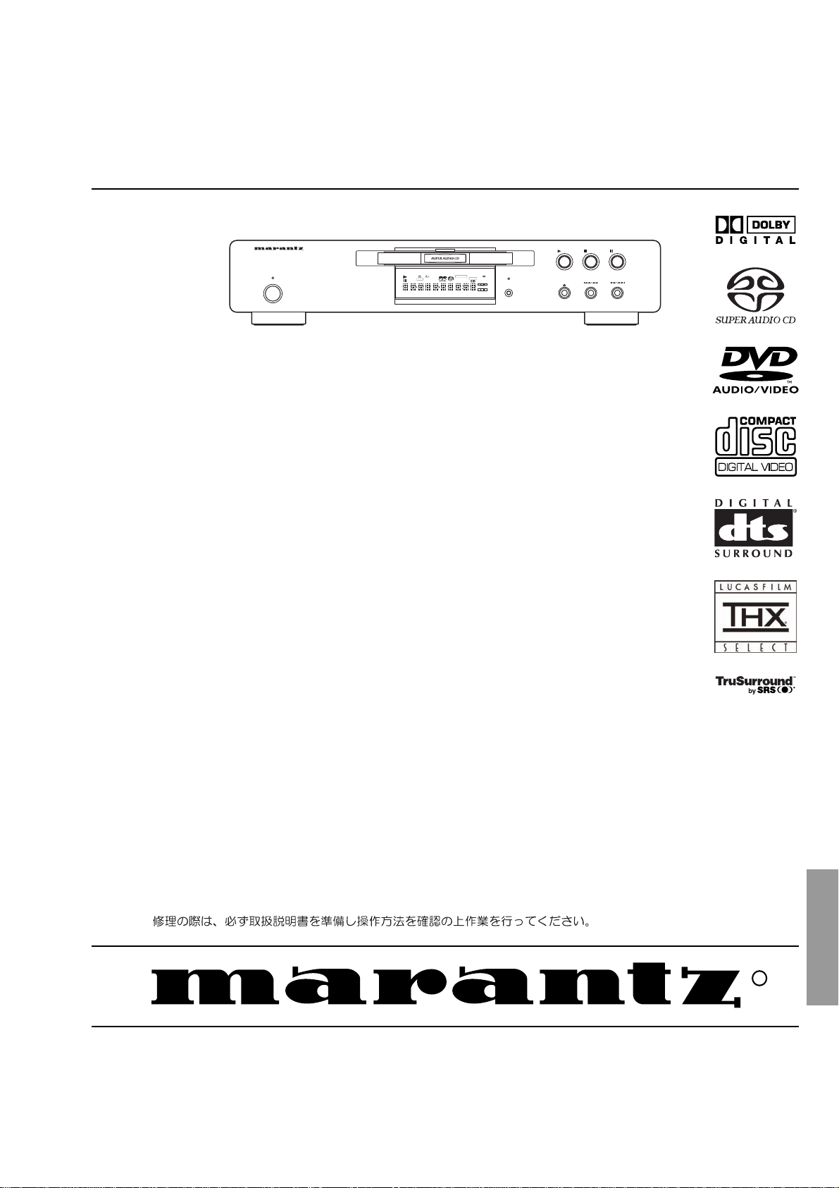
SACD/DVD PLAYER DV8300
V-PART
GRP
TITLE
PROGRESSIVE
Y D
DOLB
LAST
COND
VCD
96kHz
V OFF
TRKD OFF
CHP
5.1CH
TOTAL
REMAIN
DOWN MIX
FL OFF
R
C
L
LFE
S
LS
RS
SURROUND
192kHz
TABLE OF CONTENTS
SACD/DVD Player
STOP
PAUSEPLAY
OPEN/CLOSE
DB-VLD302 (DVD LOADER FOR MARANTZ)
2.1 LOARDING MECHANISM ASS’Y AND LOAB PCB ASS’Y......................................................2-2
2.2 TRAVERSE MECHANISM ASS’Y.............................................................................................2-5
DB-VPB305 (DVD PCB MODULE FOR MARANTZ)
3.1 DIAGRAMS (BLOCK, WIRING, SCHEMATIC, WAVEFORMS) ................................................ 3-2
3.2 PCB CONNECTION DIAGRAM.............................................................................................. 3-15
3.3 GENERAL INFOMATION (ID NUMBER., DISASSEMBLY., IC DATA).....................................3-18
3.4 PCB PARTS LIST.................................................................................................................... 3-45
Please use this service manual with referring to the user guide ( D.F.U. ) without fail.
DV8300
DV8300
R
02AK855010 MIT
First Issue 2002.06
Page 2
MARANTZ DESIGN AND SERVICE
Using superior design and selected high grade components,
Only original
MARANTZ
parts can insure that your
MARANTZ
MARANTZ
product will continue to perform to the specifi cations for which
company has created the ultimate in stereo sound.
it is famous.
Parts for your
MARANTZ
ORDERING PARTS :
equipment are generally available to our National Marantz Subsidiary or Agent.
Parts can be ordered either by mail or by Fax.. In both cases, the correct part number has to be specifi ed.
The following information must be supplied to eliminate delays in processing your order :
1. Complete address
2. Complete part numbers and quantities required
3. Description of parts
4. Model number for which part is required
5. Way of shipment
6. Signature : any order form or Fax. must be signed, otherwise such part order will be considered as null and void.
USA
MARANTZ AMERICA, INC
1100 MAPLEWOOD DRIVE
ITASCA, IL. 60143
USA
PHONE : 630 - 741 - 0300
FAX : 630 - 741 - 0301
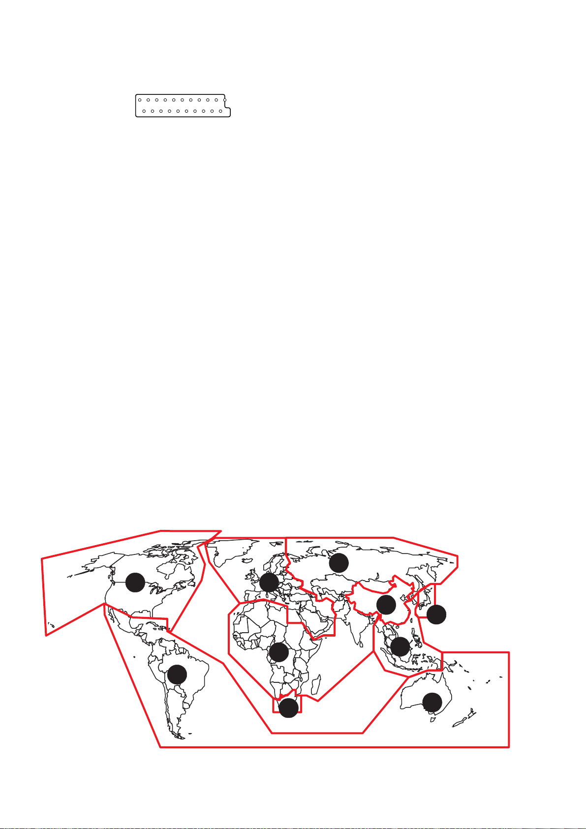
AMERICAS
SUPERSCOPE TECHNOLOGIES, INC.
MARANTZ PROFESSIONAL PRODUCTS
2640 WHITE OAK CIRCLE, SUITE A
AURORA, ILLINOIS 60504 USA
PHONE : 630 - 820 - 4800
FAX : 630 - 820 - 8103
EUROPE / TRADING
MARANTZ EUROPE B.V.
P. O. BOX 8744, BUILDING SILVERPOINT
BEEMDSTRAAT 11, 5653 MA EINDHOVEN
THE NETHERLANDS
PHONE : +31 - 40 - 2507844
FAX : +31 - 40 - 2507860
AUSTRALIA
TECHNICAL AUDIO GROUP PTY, LTD
558 DARLING STREET,
BALMAIN, NSW 2041,
AUSTRALIA
PHONE : 61 - 2 - 9810 - 5300
FAX : 61 - 2 - 9810 - 5355
CANADA
LENBROOK INDUSTRIES LIMITED
633 GRANITE COURT,
PICKERING, ONTARIO L1W 3K1
CANADA
PHONE : 905 - 831 - 6333
FAX : 905 - 831 - 6936
HONG KONG
Jolly ProAudio Broadcast Engineering Ltd.
UNIT 2, 10F, WAH HUNG CENTRE,
41 HUNG TO ROAD, KWUN TONG, KLN.,
HONG KONG
PHONE : 852 - 21913660
FAX : 852 - 21913990
AUSTRALIA
QualiFi Pty Ltd,
24 LIONEL ROAD,
MT. WAVERLEY VIC 3149
AUSTRALIA
PHONE : +61 - (0)3 - 9543 - 1522
FAX : +61 - (0)3 - 9543 - 3677
NEW ZEALAND
WILDASH AUDIO SYSTEMS NZ
14 MALVERN ROAD MT ALBERT
AUCKLAND NEW ZEALAND
PHONE : +64 - 9 - 8451958
FAX : +64 - 9 - 8463554
JAPAN
MARANTZ JAPAN, INC.
35- 1, 7- CHOME, SAGAMIONO
SAGAMIHARA - SHI, KANAGAWA
JAPAN 228-8505
PHONE : +81 42 748 1013
FAX : +81 42 741 9190
Technical
THAILAND
MRZ STANDARD CO., LTD
746 - 754 MAHACHAI ROAD.,
WANGBURAPAPIROM, PHRANAKORN,
BANGKOK, 10200 THAILAND
PHONE : +66 - 2 - 222 9181
FAX : +66 - 2 - 224 6795
TAIWAN
PAI- YUING CO., LTD.
6 TH FL NO, 148 SUNG KIANG ROAD,
TAIPEI, 10429, TAIWAN R.O.C.
PHONE : +886 - 2 - 25221304
FAX : +886 - 2 - 25630415
SHOCK, FIRE HAZARD SERVICE TEST :
SINGAPORE
WO KEE HONG DISTRIBUTION PTE LTD
130 JOO SENG ROAD
#03-02 OLIVINE BUILDING
SINGAPORE 368357
PHONE : +65 6858 5535 / +65 6381 8621
FAX : +65 6858 6078
MALAYSIA
WO KEE HONG ELECTRONICS SDN. BHD.
SUITE 8.1, LEVEL 8, MENARA GENESIS,
NO. 33, JALAN SULTAN ISMAIL,
50250 KUALA LUMPUR, MALAYSIA
PHONE : +60 3 - 21457677
FAX : +60 3 - 21458180
KOREA
MK ENTERPRISES LTD.
ROOM 604/605, ELECTRO-OFFICETEL, 16-58,
3GA, HANGANG-RO, YONGSAN-KU, SEOUL
KOREA
PHONE : +822 - 3232 - 155
FAX : +822 - 3232 - 154
CAUTION : After servicing this appliance and prior to returning to customer, measure the resistance between either primary AC
cord connector pins ( with unit NOT connected to AC mains and its Power switch ON ), and the face or Front Panel of product and
controls and chassis bottom.
Any resistance measurement less than 1 Megohms should cause unit to be repaired or corrected before A C po wer is applied, and
verifi ed before it is return to the user/customer.
Ref. UL Standard No. 1492.
In case of diffi culties, do not hesitate to contact the Technical
Department at above mentioned address.
020326MIT
Page 3

1. TECHNICAL SPECIFICATIONS
General
System.....................................DVD-Video, DVD-Audio, DVD-R/RW,
Video-CD, SACD, CD and MP3 fi les
Power requirements
A Version .............................................................AC 240 V, 50 Hz
C Version .............................................................AC 220 V, 60 Hz
F Version.......................................................AC 100 V, 50 / 60 Hz
K Version .............................................................AC 220 V, 50 Hz
L Version..............................................................AC 110 V, 60 Hz
N Version .............................................................AC 230 V, 50 Hz
S Version ......................................................AC 230 V, 50 / 60 Hz
U Version .............................................................AC 120 V, 60 Hz
Power consumption
F Version................................................................................18 W
L Version................................................................................19 W
Other Version.........................................................................20 W
Weight
N Version ........................................................6.2 kg (13 lb 44 oz)
Other Version..................................................6.1 kg (13 lb 44 oz)
Dimensions.......................................440 (W) x 307 (D) x 89 (H) mm
(17 8/25 (W) x 12 2/25 (D) x 3 1/2 (H) in.)
(Not including protruding cables, etc.)
Operating temperature ...............+5 °C to +35 °C (+41 °F to +96 °F)
Operating humidity .............................5% to 85% (no condensation)
S-Video output
Y (luminance) - Output level.......................................1 Vp-p (75 Ω )
C (color) - Output level : NTSC............................286 mVp-p (75 Ω )
: PAL ...............................300 mVp-p (75 Ω )
Jacks ..........................................................................S-VIDEO jack
Video output (2 individual outputs)
Output level.................................................................1 Vp-p (75 Ω )
Jacks ..................................................................................RCA jack
Component video output (Y, C
B/PB, CR/PB)
Output level.........................................................Y : 1.0 Vp-p (75 Ω )
C
B/PB, CR/PB : 0.7 Vp-p (75 Ω )
Jacks ..................................................................................RCA jack
Audio output (2 individual outputs)
Output level
During audio output.............................. 200 mVrms (1 kHz, –20 dB)
Number of channels ........................................................................2
Jacks ..................................................................................RCA jack
Audio output (multi-channel / L, R, C, SW, LS, RS)
Output level
During audio output.............................. 200 mVrms (1 kHz, –20 dB)
Number of channels ........................................................................6
Jacks ..................................................................................RCA jack
Digital audio characteristics
Frequency response.......................4 Hz to 44 kHz (DVD fs: 96 kHz)
4 Hz to 88 kHz (DVD-Audio fs: 192 kHz)
S/N ratio................................................................ more than 118 dB
Dynamic range ..................................................... more than 108 dB
Total harmonic distortion.......................................................0.001%
Wow and fl utter............... Limit of measurement(–0.001% W. PEAK)
or lower
Digital output
Optical digital output.............................................Optical digital jack
Coaxial digital output..........................................................RCA jack
Accessories
Audio/Video cord.............................................................................1
System Control cord........................................................................1
Power Cord......................................................................................1
Remote control unit .........................................................................1
AA (R6P) dry cell batteries..............................................................2
Operating Instructions .....................................................................1
Note
The specifi cations and design of this product are subject to change
without notice, due to improvement.
R / G / B output
Output level..............................................R / G / B : 0.7 Vp-p (75 Ω )
Jacks (N Version).......................................21 pin SCART connector
D1/D2 video output (except for N, U Version)
Output level.........................................................Y : 1.0 Vp-p (75 Ω )
C
B/PB, CR/PB : 0.7 Vp-p (75 Ω )
Jacks ................................................................................ D terminal
1
Page 4
2. CONNECTION FACILITIES
2.1 Video performance (/N only)
135791113151719
21
2. 1. 1 SCART
2 4 6 8 10 12 14 16 18 20
Pin No. TV (OUT) Pin No. AUX (IN)
Pin 1 Audio R out : 2Vrms Pin 1 Audio R out : 2Vrms
Pin 2 Audio R in : 2Vrms Pin 2 Audio R in : 2Vrms
Pin 3 Audio L out : 2Vrms Pin 3 Audio L out : 2Vrms
Pin 4 GND Pin 4 GND
Pin 5 GND Pin 5 GND
Pin 6 Audio L in : 2Vrms Pin 6 Audio L in : 2Vrms
Pin 7 Blue out/C in Pin 7 Blue in/C out
Pin 8 function switching out <2V : TV Pin 8 function switching in<2V : DVD
Pin 9 GND Pin 9 GND
Pin 10 not connected Pin 10 not connected
Pin 11 Green out:0.7Vpp ±0.1V into 75 Ohm *1 Pin 11 Green in:0.7Vpp ±0.1V into 75 Ohm
Pin 12 not connected Pin 12 not connected
Pin 13 GND Pin 13 GND
Pin 14 GND Pin 14 GND
Pin 15 Red/C out Pin 15 Red/C in
Pin 16 fast switching out <0.4V into 75 Ohm=CVBS/S-Video Pin 16 fast switching in <0.4V into 75 Ohm=CVBS/S-Video
1</<3 into 75 Ohm=RGB 1</<3 into 75 Ohm=RGB
Pin 17 GND Pin 17 GND
Pin 18 GND Pin 18 GND
Pin 19 CVBS/Y out : 1Vpp ±0.1V *1 Pin 19 CVBS/Y out : 1Vpp ±0.1V *1
Pin 20 CVBS/Y in : 1Vpp ±0.1V *1 Pin 20 CVBS/Y in : 1Vpp ±0.1V *1
Pin 21 GND Pin 21 GND
Blue : 0.7Vpp ±0.1V into 75 Ohm *1 Blue : 0.7Vpp ±0.1V into 75 Ohm *1
C : 300mVpp ±30 into 75 Ohm *2 C : 300mVpp ±30 into 75 Ohm *2
>5/<8 : asp.ratio 16 : 9 DVD/AUX >5/<8 : asp.ratio 16 : 9 AUX
>9.5/<12 : asp.ratio 4 : 3 DVD/AUX >9.5/<12 : asp.ratio 4 : 3 AUX
Red : 0.7Vpp ±0.1V into 75 Ohm *1 Red : 0.7Vpp ±0.1V into 75 Ohm *1
C : 300mVpp ±30 into 75 Ohm *2 C : 300mVpp ±30 into 75 Ohm *2
*1 : 100% White *2 : Burst Level *3 : color bar(chroma level : 75%)
What are "regional codes"?
Motion picture studios want to control the home release of movies in different countries because theater releases arenit
simultaneous (a movie may come out on DVD in the US when itis just hitting screens in Europe). Therefore they have
required that the DVD standard include codes which can be used to lock out the playback of certain discs in certain geographical regions. Players sold in each region will have that regionis code built into the player. The player will refuse to play
these "region coded" discs which are not allowed in the region. However, regional codes are entirely optional. Discs without
codes will play on any player in any country. Some studios have already announced that only their new releases will have
regional codes. There are six regions:
1. United States and Canada 2. Europe and Japan
3. Far East (except Japan & China) 4. South America and Oceania
5. Africa and the Middle East 6. China (except Hong Kong)
5
1 2
6
2
5
3
4
2
Map of DVD Regions
2
4
Page 5
y.)
3. INFORMATIONS
REGION CODE
VERSION REGION CODE COUNTRY
/UXX 1 USA/CANADA
/FXX 2 JAPAN
/NXX 2 EUROPE
/CXX 3 KOREA
/LXX 3 TAIWAN
/SXX 3 SINGAPORE/HONGKONG
/AXX 4 AUSTRALIA
/KXX 6 CHINA
DVD INFORMATION
Below is a glossary of the new terms related to DVD.
Title:
A disc may have more than one story/movie on it, so each
story/movie is called a
For example, if there are 2 movies on the disc, they are
separated into Title 1 and Title 2.
Chapter:
A title may also be separated into chapters.
For example, a movie (title) may be separated into 3 scenes
(chapters).
Title 1 Title 2
Chapter1Chapter
2
Subtitles:
DVDs are recorded with up to 32 different subtitle languages.
If a disc has more than one subtitle language, you can select
the subtitle language that you want to read.
Soundtrack language:
DVDs are recorded with up to 8 diff erent soundtrac k languages.
If a disc has more than one language, you can select the
soundtrack language that you want to listen to.
"
title".
Chapter3Chapter1Chapter2Chapter
3
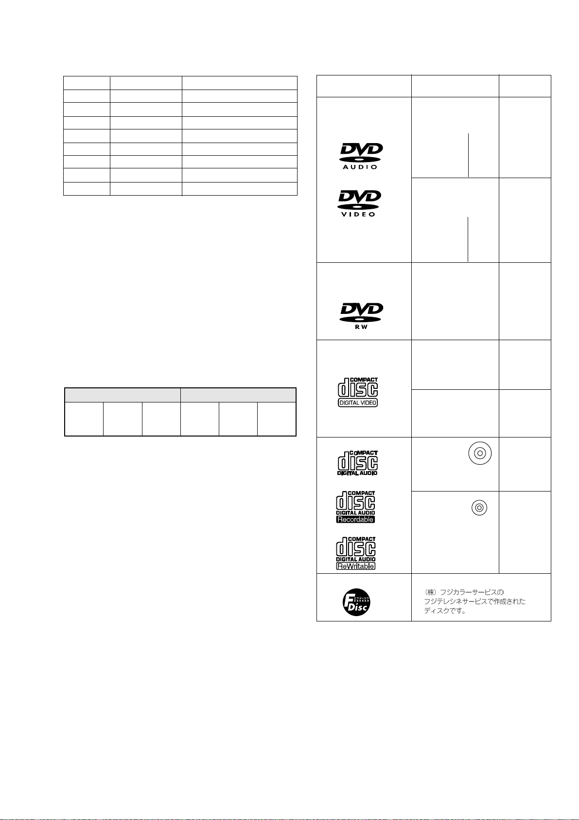
THE DISCS THAT THE DV8300 CAN HANDLE
The following discs can be played back with a DV-12S1
Types of playable
discs and their marks
DVD-Audio
DVD-Video
DVD-RW
(JAPAN & USA model only)
*
VIDEO CD
CD
**
**
F-Disc (F only)
Diameter/
Playable sides
DVD-Audio
DVD-Video
12 cm (5in.)/
single-sided
12 cm (5in.)/
double-sided
DVD-Audio
DVD-Video
8 cm (3 in.)/
single-sided
8 cm (3 in.)/
double-sided
DVD-RW
12 cm (5in.)/
single-sided
8 cm (3 in.)/
single-sided
VIDEO CD
12 cm (5 in.)/
single-sided
VIDEO CD single
8 cm (3 in.)/
single-sided
CD
12 cm (5 in.)/
single-sided
CD single
8 cm (3 in.)/
single-sided
1 layer
2 layer
1 layer
2 layer
1 layer
2 layer
1 layer
2 layer
Playback time
Digital audio
Digital video
(MPEG 2)
133 min.
242 min.
266 min.
484 min.
Digital audio
Digital video
(MPEG 2)
41 min.
75 min.
82 min.
150 min.
Digital audio
Digital video
(MPEG 2)
Max. 360 min.
Max. 100 min.
Digital audio
Digital video
(MPEG 1)
Max. 74
minutes
Digital audio
Digital video
(MPEG 1)
Max. 20
minutes
Digital audio
Max. 74
minutes
Digital audio
Max. 20
minutes
Multi-angles:
On some D
VDs, scenes have been filmed from diff erent angles
(up to a maximum of 9). On these discs, you can select the
angle that you want to watch. Please ref er to the D V D's manual
to see which scenes have multi-angles.
Resetting the Player to System Settings:
To reset the player, press and hold [STOP] button on the front
panel when pressing Power switch to turn the power on.
All program memory, saved settings from functions such as
Last Memory and Condition Memory are cleard, and all Setup
screen menus are returned to factory settings.
Note:The regional code of the discs must meet to the regional
code of the DV8300
The disc format logos shown above are found on disc labels or on disc jackets.
•
To prevent malfunction, do not use an 8 cm (3 in.) adaptor (for CDs).
•
Discs other than the ones indicated above cannot be played on this unit.
•
DVDs that have incompatible region numbers, DVDROM, DVD-RAM, and CD-ROM cannot be
played on this unit. The region number of the player can be found on the rear panel.
* Playing DVD-RW discs (JAPAN & USA model only)
•
You may not be able to play non-finalized DVD-RW discs.
•
Copyrighted content originally provided with the permission of one generation and recorded on
•
DVD discs cannot be played on this player.
•
When playing a DVD-RW disc that was edited on a DVD recorder, you may see scenes from just
before the edited point. This is not a malfunction.
•
Up to 20 characters of a title name can be displayed.
** Playing recordable CDs
•
Note that this unit cannot record onto recordable discs.
•
This unit can play music-use CD-R and CD-RW discs.
However, depending on the condition of the CD-Recorder and the disc, you may find that not all
discs will play successfully. (For example, if the disc is scratched or dirty, or if the player fs pickup
3
lens is dirt
Page 6
4. SERVICE HINTS AND TOOLS
SERVICE HINTS
SERVICE TOOLS
Audio signals disc 4822 397 30184
Disc without errors (SBC444)+
Disc with DO errors, black spots and fingerprints (SBC444A) 4822 397 30245
Disc (65 min 1kHz) without no pause 4822 397 30155
Max. diameter disc (58.0 mm) 4822 397 60141
Torx screwdrivers
Set (straight) 4822 395 50145
Set (square) 4822 395 50132
13th order filter 4822 395 30204
DVD test disc (PAL) 4822 397 10131
DVD test disc (NTSC) ALMEDIO TDV-540
4
Page 7
5. WARNING AND LASER SAFETY INSTRUCTIONS
GB
WARNING
All ICs and many other semi-conductors are
susceptible to electrostatic discharges (ESD).
Careless handling during repair can reduce
life drastically.
When repairing, make sure that you are
connected with the same potential as the
mass of the set via a wrist wrap with
resistance.
Keep components and tools also at this
potential.
F
ATTENTION
D
WARNUNG
I
WAARSCHUWING
AVVERTIMENTO
NL
Alle IC’s en vele andere halfgeleiders zijn
gevoelig voor elektrostatische ontladingen
(ESD).
Onzorgvuldig behandelen tijdens reparatie
kan de levensduur drastisch doen
verminderen.
Zorg ervoor dat u tijdens reparatie via een
polsband met weerstand verbonden bent met
hetzelfde potentiaal als de massa van het
apparaat.
Houd componenten en hulpmiddelen ook op
ditzelfde potentiaal.
Tous les IC et beaucoup d’autres semiconducteurs sont sensibles aux décharges
statiques (ESD).
Leur longévité pourrait être considérablement
écourtée par le fait qu’aucune précaution
n’est prise a leur manipulation.
Lors de réparations, s’assurer de bien être
relié au même potentiel que la masse de
l’appareil et enfiler le bracelet serti d’une
résistance de sécurité.
Veiller a ce que les composants ainsi que les
outils que l’on utilise soient également a ce
potentiel.
Alle IC und viele andere Halbleiter sind
empfindlich gegen elektrostatische
Entladungen (ESD).
Unsorgfältige Behandlung bei der Reparatur
kann die Lebensdauer drastisch vermindern.
Sorgen sie dafür, das Sie im Reparaturfall
über ein Pulsarmband mit Widerstand mit
dem Massepotential des Gerätes verbunden
sind.
Halten Sie Bauteile und Hilfsmittel ebenfalls
auf diesem Potential.
GB
Safety regulations require that the set be restored to its original condition
and that parts which are identical with those specified be used.
NL
Veiligheidsbepalingen vereisen, dat het apparaat in zijn oorspronkelijke
toestand wordt terug gebracht en dat onderdelen, identiek aan de
gespecifieerde worden toegepast.
F
Les normes de sécurité exigent que l’appareil soit remis a l’état d’origine et
que soient utilisées les pièces de rechange identiques à celles spécifiées.
Tutti IC e parecchi semi-conduttori sono
sensibili alle scariche statiche (ESD).
La loro longevita potrebbe essere fortemente
ridatta in caso di non osservazione della piu
grande cauzione alla loro manipolazione.
Durante le riparazioni occorre quindi essere
collegato allo stesso potenziale che quello
della massa dell’apparecchio tramite un
braccialetto a resistenza.
Assicurarsi che i componenti e anche gli
utensili con quali si lavora siano anche a
questo potenziale.
D
Bei jeder Reparatur sind die geltenden Sicherheitsvorschriften zu beachten.
Der Originalzustand des Gerats darf nicht verandert werden.
Fur Reparaturen sind Original-Ersatzteile zu verwenden.
I
Le norme di sicurezza esigono che l’apparecchio venga rimesso nelle
condizioni originali e che siano utilizzati pezzi di ricambiago idetici a quelli
specificati.
SHOCK, FIRE HAZARD SERVICE TEST:
CAUTION: After servicing this appliance and prior to returning to customer, measure the resistance between
either primary AC cord connector pins (with unit NOT connected to AC mains and its Power switch ON), and the
face or Front Panel of product and controls and chassis bottom,
Any resistance measurement less than 1 Megohms should cause unit to be repaired or corrected before AC
power is applied, and verified before return to user/customer.
Ref.UL Standard NO.1492.
NOTE ON SAFETY:
Symbol
: Fire or electrical shock hazard. Only original parts should be used to replace any part with symbol
Any other component substitution(other than original type), may increase risk or fire or electrical shock hazard.
“Pour votre sécurité, ces documents
doivent être utilisés par des
spécialistes agrées, seuls habilités à
réparer votre appareil en panne.”
5
Page 8
LASER SAFETY
This unit employs a laser. Only a qualified service person should remove the cover or attempt to service this
device, due to possible eye injury.
LASER DEVICE UNIT
Type: Semiconductor laser GaAlAs
Wave length: 650 nm (DVD)
780 nm (VCD/CD)
Output Power: 7 mW (DVD)
10 mW (VCD/CD)
Beam divergence: 60 degree
USE OF CONTROLS OR ADJUSTMENTS OR PERFORMANCE OF PROCEDURE OTHER THAN THOSE
SPECIFIED HEREIN MAY RESULT IN HAZARDOUS RADIATION EXPOSURE.
AVOID DIRECT EXPOSURE TO BEAM
WARNING
The use of optical instruments with this product will increase eye hazard.
Repair handling should take place as much as possible with a disc loaded inside the player
WARNING LOCATION: INSIDE ON LASER COVERSHIELD
CAUTION VISIBLE AND INVISIBLE LASER RADIATION WHEN OPEN AVOID EXPOSURE TO BEAM
ADVARSEL SYNLIG OG USYNLIG LASERSTRÅLING VED ÅBNING UNDGÅ UDSÆTTELSE FOR STRÅLING
ADVARSEL SYNLIG OG USYNLIG LASERSTRÅLING NÅR DEKSEL ÅPNES UNNGÅ EKSPONERING FOR STRÅLEN
VARNING SYNLIG OCH OSYNLIG LASERSTRÅLNING NÄR DENNA DEL ÄR ÖPPNAD BETRAKTA EJ STRÅLEN
VARO! AVATTAESSA OLET ALTTIINA NÄKYVÄLLE JA NÄKYMÄTTÖMÄLLE LASER SÄTEILYLLE. ÄLÄ KATSO SÄTEESEEN
VORSICHT SICHTBARE UND UNSICHTBARE LASERSTRAHLUNG WENN ABDECKUNG GEÖFFNET NICHT DEM STRAHL AUSSETSEN
DANGER VISIBLE AND INVISIBLE LASER RADIATION WHEN OPEN AV OID DIRECT EXPOSURE TO BEAM
ATTENTION RAYONNEMENT LASER VISIBLE ET INVISIBLE EN CAS D'OUVERTURE EXPOSITION DANGEREUSE AU FAISCEAU
6
Page 9
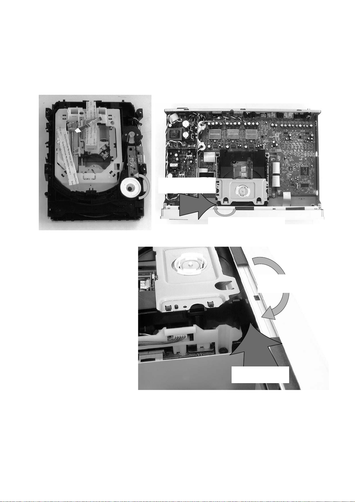
6. TAKING THE DISC OUT OF EMERGENCY
1. Remove 6 screws on the top cover and remove the top cover.
2. Put a fi nger is under the mechanism and Turn the gear to the direction with your fi nger.
3. The disc tray will opened.
Put a fi nger is under
the mechanism
Turn the gear to the direction
with your fi nger
Turn the gear to the direction
Put a fi nger is under
the mechanism
with your fi nger
7
Page 10
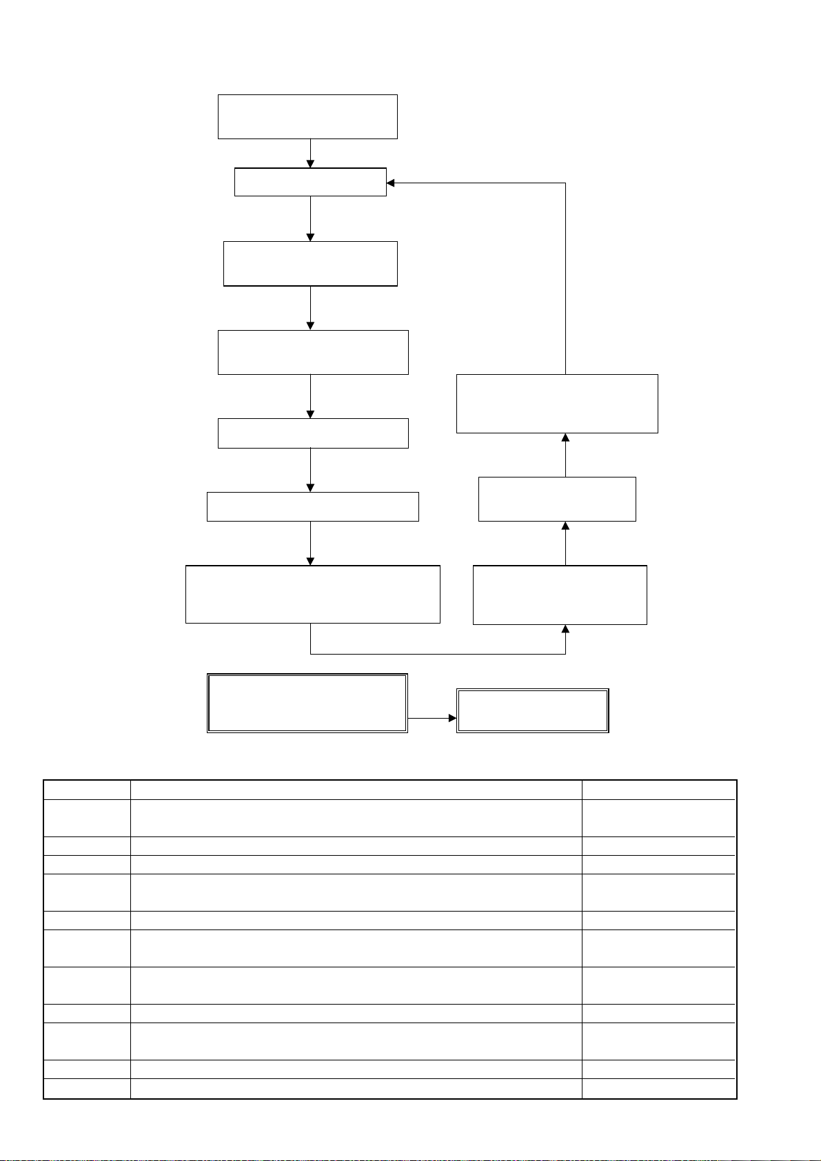
7. SERVICE MODE AND TROUBLE SHOOTING
SERVICE MODE
Press<POWER>while pressing
<PAUSE>and<STOP>
“TEST 1” is displayed
Press<NEXT >
STANDBY LED Light on RED
“
STB_LED” is displayed
Press<NEXT >
FL OFF LED Light on RED
“FL_OFF_LED ” is displayed
Press<NEXT >
All parts of LED is turned on
Press<NEXT >
Each Segment is displayed one by one
Press< NEXT >
STANDBY LED and FL OFF LED Light on RED
ILM LED light on Blue Check of key When key is
depressed,key name is displayed
Press<PAUSE>and<STOP>
Power on without Disc
after
<Fast Forward>and<Fast Reverse>
Press<NEXT >
MS code is displayed
“MSO X” is displayed
MS code is not necessary for service
Press<NEXT >
Region code is displayed
“XXX X” is displayed
Press<NEXT >
Version of Front uP
(SYM No.QF01)is displayed
“M VERXXXX” is displayed
Region code is displayed
“XXX X” is displayed
ERROR CODE
Error codes are displayed on the FL display.
FL Display Possible causes Operation of the unit
AV1 VER AV-1 chip is not a match with program of system controller.
The sound may not out
with the specific audio.
CPU AERR CPU address error. (Hardware is unusual.) No operation.
DMA AERR DMA address error. (Hardware is unusual.) No operation.
FLASH ID
Difference in versions of the internal ROM of the system controller and of the
flash ROM, or bus line failure or reverse installation.
No operation.
FLASH WRP Write protect error of the flash ROM. No operation.
FLASH SIG
FLASH SUM
Difference in part number of the flash ROM.
(When the ROM which couldn't be used was used.)
Check sum error of the flash ROM (It exceeds the regular size.) or
reverse installation. (Hardware is unusual.)
No operation.
No operation.
FLASH SIZE Size error of the flash ROM. (Use 4 or 8 M-bit.) No operation.
ILLGAL
The system controller fetched a code other than an operation code.
(Hardware is unusual.)
No operation.
RESERVE Undefined interrupt. (Hardware is unusual.) No operation.
SLOT Inappropriate slot command issued. (Hardware is unusual.) No operation.
8
Page 11
• T o Confi rm version of System uP. on DVDM.
Press Basic icom under the General item in the Setup Menu
Press Power ON
Press SETUP key on R.C.
Press DISPLAY key on R.C.
Version of System uP. is displayed
"Region : X / Ver : XXXX(XX) / AV1 : x.x / x.x" is displayed
The version displayed here is a version written in the system microprocessor of DVDM (002A).
Change of this version by external operation cannot be performed.
9
Page 12
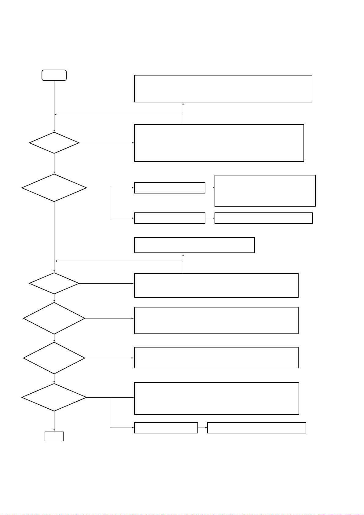
TROUBLE SHOOTING
• No Power ON
• FL is not turned ON
• FL indication is unusual
START
Turn on the power again
after 2 - 3 minutes.
Is FL turn on ?
Yes
Is the indication
of FL normal ?
Yes
Power ON
No
No
• Blow out fuse of the primary side (FP01)
• Blow out micro-fuse on the PS01. (Check the each voltage.)
(FP02, FP02)
• FL controller IC (QF01) on the PF01 is damaged.
• Check the following connections :
PS01-PS02, PS01-PD01, PD01-DVDM Assy, PD01-PM01, PM01-PF01
Check each voltage (EV+5V, SW+5V, SW+3.3V, SW+12V, M+6V, -28V
•
DC+3.5V and Heater)
(If above voltage are not supplied, check the micro-fuse FP02, FP03.)
• Short or open the zenner diode
FL indication is dark or flickers.
Indicates the error message
• Blow out micro-fuse on the PS01.
(FP03)
on the PS01.
(DP05, DP06, DP08 - DP10, DP19, DP20)
• Check the values of RP29
on the PS01.
Refer to the section "ERROR CODE".
Is tray open ?
Yes
Spindle
does not turn.
Carriage does
not move.
Yes
Laser diode
does not light.
Focus does
not in.
Yes
Do the video and
sound come on ?
Yes
OK
No
No
No
No
• Check the following connections :
DVDM Assy - LOAB Assy (5P connector assy)
• Check the voltage of +6V and +12V power supply
• Check the following connections :
DVDM Assy - Spindle motor (12P flexible cable)
DVDM Assy - Stepping motor (4P flexible cable)
• Check the voltage of +6V and +12V power supply
• Check the following connection :
DVDM Assy - Pickup Assy (26P flexible cable)
• Check the voltage of +6V and +12V power supply and SW+5V
• Check the following connection :
PD01-DVDM Assy, PD01-PM01, PS01-PM01
• Check each voltage. (EV+5V, SW+5V, SW+3.3V, SW+12V,+8VA, -8VA)
(If above voltage are not supplied, check the micro-fuse FP03, FP50,
FP51)
Indicate the error message.
Refer to the section "ERROR CODE".
10
Page 13
8. WIRING DIAGRAM
JP50 J202
1
+3.3VD
2
A-GND
3
A-GND
4
+5VA
5
P_MUTE
6
-8VA
JP51 J208
121
-8VA
+8VA
JP52 J207
1
+8VA
2
A-GND
3
A-GND
4
-8VA
ONLY N
J851
V
12
V-GND
V-MUTEV_MUTE
123456789101112131415
V-GND
V-GND
V-GND
RGB SW
F-SW
+12VV
A-GND
11
V/Y
10
9
R/C
8
7
G
6
5
B
4
3
2
1
J204
1
SAL
2
3
SAR
1
+3.3VDD
2
DAC-GND
3
DAC-GND
4
+5VDA
5
PMUTE
6
-8VDA
PM01
-8VAA
2
+8VAA
1
+8VA
2
GND
3
GND
4
-8VA
GND
XCSDF0
MCLK1
DSDCLKOUT1
LRCKOUT1
BCK/DSD-R
DATA0/DSD-L
XAMUTE
XFRSTO
GND
MCLK2
DSDCLKOUT2
LRCKOUT2
BCK/DSD-RS
DATA1/DSD-LS
XMMUTE
GND
XCSDF1
XDFSCK
MCLK3
XDFS0
DSDCLKOUT3
LRCKOUT3
BCK/DSD-SW
DATA2/DSD-C
XFRST1
GND
GND
GND
212223
24
20
101112
13251426152716281729183019
123456789
SW+5V
D_OUT
D-GND
VSEL2
SQUEEZE
LETTER
VSEL1
D-GND
SDA0
SCL0
D-GND
D-GND
AV1CLK
D-GND
D-GND
XVQERST
VSYNC
HSYNC
PD0
PD1
PD2
PD3
PD4
PD5
PD6
PD7
XCSPRO2
VQESSO
VQESCK
JE01J705
212223
24
20
101112
13251426152716281729183019
D-GND
123456789
D-GND
CTS
DTR
RXD
TXD
XREADY
SSCK
S(FtoM)
S(MtoF)
XRESET
LT1
D-GND
SW+12V
SW+12V
V-GND
V-GND
E+5V
E+5V
V-GND
V-GND
SW+3.3V
SW+3.3V
D-GND
D-GND
STB_CTL
E+5V
HEATER
DC+3.5V
-28V
D-GND
101112
212223
24
20
13251426152716281729183019
123456789
D-GND
-28V
DC+3.5V
HEATER
E+5V
STB_CTL
D-GND
P_TRG
LT1
XRESET
S(MtoF)
S(FtoM)
SSCK
XREADY
D-GND
/TEST
D-GND
IR_SW
1617181920
D-BUS
AC Inlet
LIVE
NEUTRAL
BCK/DSD-RS
DATA1/DSD-LS
CN401
1
3
5
7
9
LRCKOUT2
2
4
6
8
10
12
14
16
18
20
22
24
26
28
30
32
34
36
38
40
DSDCLKOUT2
MGND
SW+5V
MGND
GND
M+6V
GND
M+6V
SW+3.3V
12V
SW+3.3V
GND
SW+2.5V
GND
SW+2.5V
GND
GND
GND
DACCLK
NC
GND
NC
XCSAQE
GND
XAQRST
D_OUT
XDFSO
XAMYTE
XDFSCK
XMMUTE
GND
DATA1
BCK
DATA2
GND
XCSDF1
DATA0
XFRST1
LRCK
XFRST0
XCSDF0
MCLK2
20
GND
212223
XAMUTE
24
XFRSTO
LRCKOUT1
BCK/DSD-R
DATA0/DSD-L
Carriage motor
CN104
GND
GND GND
MCLK1
XCSDF0
DSDCLKOUT1
DB-VLD302
ST1-
4
123
ST1-
ST2-
ST1+
ST1+
ST2-
V+3D
SW2
GNDS
ST2+
123
4
CN103 CN601
SW2
ST2+
GNDS
V+3D
123456789
VSEL2
D-GND
D_OUT
SW+5V
SQUEEZE
LETTER
DB-VPB305
DVDM
MECHA
A2
A3
LOAB-
LOAB+
LOAB+
LOAB-
H1+
A1
Spindle motor
12345
101112
12345
123456789
CN105
A3A2A1
H1+
VSEL1
H1-
H1-
D-GND
H2+
H2+
SDA0
H2-
H2-
101112
SCL0
H3+
H3+
13251426152716281729183019
D-GND
D-GND
D-GND
AV1CLK
H3-
INSIDE
V+5S
GNDS
101112
H3-
GNDS
V+5S
INSIDE
D-GND
123456789
CN101 CN0000
123456789
J703 J201
GND
GND
GND
XFRST1
JP01
J001
1
1
LIVE
2
2
NEUTRAL
PS01
JP05 J701
-28V -28V
DC+3.5V
HEATER
E+5V
STB_CTL
SW+3.3V
SW+3.3V
JP10
1
2
SW+3.3V
SW+3.3V
JP11
1
2
LIVE LIVE
NEUTRAL NEUTRAL
SW+5V
SW+5V
M+6V
M+6V
M+6V
M-GND
M-GND
M-GND
SW+12V
SW+12V
1
2
JP02
1
2
JP08
1
30
2
DC+3.5V
29
3
HEATER
28
4
E+5V
27
5
STB_CTL
26
6
GND
GND
GND
GND
GND
GND
GND
GND
GND
GND
GND
GND
25
7
SW+3.3V
24
8
SW+3.3V
23
9
SW+3.3V
22
10
SW+3.3V
21
11
GND
20
12
GND
19
13
GND
18
14
GND
17
15
SW+5V
16
16
SW+5V
15
17
GND
14
18
GND
13
19
GND
12
20
GND
11
21
M+6V
10
22
M+6V
9
23
M+6V
8
24
M-GND
7
25
M-GND
6
26
M-GND
5
27
GND
4
28
GND
3
29
SW+12V
2
30
SW+12V
1
DATA2/DSD-C
BOARD TO BOARD CONNECTOR
MGND
2
SW+5V
MGND
4
GND
M+6V
6
GND
M+6V
8
SW+3.3V
12V
10
SW+3.3V
GND
12
SW+2.5V
GND
14
SW+2.5V
GND
16
GND
GND
18
DACCLK
NC
20
GND
NC
22
XCSAQE
GND
24
XAQRST
D_OUT
26
XDFSO
XAMYTE
28
XDFSCK
XMMUTE
30
GND
DATA1
32
BCK
DATA2
34
GND
XCSDF1
36
DATA0
XFRST1
38
LRCK
XFRST0
40
XCSDF0
XMSLAT2
2
GND
33MSACD
4
GND
BCLK
6
GND
XSAK
8
BD0
BD1
10
BD2
BD3
12
BD4
XDFSO
14
XDFSCK
XDFSI
16
XSRQ
XMSLAT
18
DSPA2
GND
20
GND
VCOSCD
22
GND
GND
24
RFSACD
GND
26
RD1
RD2
28
RD3
RD4
30
RD5
RD6
32
RD7
RD8
34
XSHD
BD7
36
BD6
BD5
38
XMSREADY
XMRST
40
XSACDSL
101112
XDFS0
MCLK3
XDFSCK
LRCKOUT3
BCK/DSD-SW
DSDCLKOUT3
J702
1
3
5
7
9
11
13
15
17
19
21
23
25
27
29
31
33
35
37
39
J601 CN602
1
1
3
3
5
5
7
7
9
9
11
11
13
13
15
15
17
17
19
19
21
21
23
23
25
25
27
27
29
29
31
31
33
33
35
35
37
37
39
39
13251426152716281729183019
GND
XCSDF1
XMMUTE
11
13
15
17
19
21
23
25
27
29
31
33
35
37
39
XMSLAT2
2
GND
33MSACD
4
GND
BCLK
6
GND
XSAK
8
BD0
BD1
10
BD2
BD3
12
BD4
XDFSO
14
XDFSCK
XDFSI
16
XSRQ
XMSLAT
18
DSPA2
GND
20
GND
VCOSCD
22
GND
GND
24
RFSACD
GND
26
RD1
RD2
28
RD3
RD4
30
RD5
RD6
32
RD7
RD8
34
XSHD
BD7
36
BD6
BD5
38
XMSREADY
XMRST
40
XSACDSL
PS02
VSYNC
XVQERST
TRKG DRV
FCCS RTN
FCCS RTN
TRKG DRV
HSYNC
TRKG RTN
24
24
TRKG RTN
20
212223
24
PD1
PD0
PD5
PD4
PD3
PD2
PD7
PD6
D-GND
VQESSO
VQESCK
XCSPRO2
123456789
J706 JE02
CTS
DTR
TXD
RXD
D-GND
XREADY
SSCK
S(FtoM)
101112
S(MtoF)
XRESET
S(M-TO-F)
S(F-TO-M)
SSCK
XREADY
GND
XCSVE5
VQESCK
VQESSO
XCSPRO2
PD(7)
PD(6)
PD(5)
PD(4)
PD(3)
PD(2)
PD(1)
PD(0)
HSYNC
VSYNC
XVQERST
GND
AV1CLK
GND
SCL0
SDA0
P/XN
GND
VSEL1
LETTER
SQUEEZE
VSEL2
GND
XRESET
LT1
TXD
RXD
DTR
CTS
GND
GND
LT1
D-GND
2
4
6
8
10
12
14
16
18
20
22
24
26
28
30
32
34
36
38
40
13251426152716281729183019
V-GND
SW+12V
SW+12V
1
3
5
7
9
11
13
15
17
19
21
23
25
27
29
31
33
35
37
39
V-GND
E+5V
E+5V
20
212223
24
V-GND
V-GND
D-GND
D-GND
SW+3.3V
SW+3.3V
BOARD TO BOARD CONNECTOR
J704CN501
1
LT1
2
XRESET
3
TXD
4
S(M-TO-F)
5
RXD
6
S(F-TO-M)
7
DTR
8
SSCK
9
CTS
10
XREADY
11
GND
12
N.C.
13
VQESCK
14
VQESSO
15
XCSPRO2
16
PD(7)
17
PD(6)
18
PD(5)
19
PD(4)
20
PD(3)
21
PD(2)
22
PD(1)
23
PD(0)
24
HSYNC
25
VSYNC
26
XVQERST
27
GND
28
GND
29
AV1CLK
30
GND
31
GND
32
SCL0
33
SDA0
34
N.C.
35
GND
36
VSEL1
37
LETTER
38
SQUEEZE
39
VSEL2
40
GND
STB_CTL
123456789
JF01 JE03
-28V
E+5V
D-GND
DC+3.5V
HEATER
D-GND
-28V
E+5V
Heater
DC+3.5V
D-GND
STB CONT
P_TRG
LT1
1011121314
XRESET
S(MtoF)
S(FtoM)
SSCK
15
D-GND
XREADY
1617181920
IR_SW
/TEST
D-GND
D-BUS
PF01
STB_LEDSTB_LED
GNDGND
1
2
1
2
JF03 JF02
PF02
J803
+12VV
12
F-SW
11
RGB SW
10
B
9
V-GND
8
G
7
V-GND
6
R/C
5
PE01
RF-
B1
B2
1/2SW
A
FCCS DRV
212223
20
20
212223
A
B2
B1
1/2SW
FCCS DRV
C
VRREF(2.5V)
C
VRREF(2.5V)
GND
B3
B4
B4
B3
GND
GND
GND
RF+
GND
132514261516171819
132514261516171819
RF-
GND
RF+
GND
LD(780)
VCC
101112
101112
GND
GND
VCC
GND
LD(780)
MPD(780)
VSHF
VSHF
MPD(780)
MPD-VR
MPD-VR
LD(650)
LD(650)
MPD(650)
123456789
123456789
MPD(650)
(ONLY N)
PD01
V-GND
V-GND
A-GND
4
V/Y
3
2
V
1
J950
1
SAL
2
3
SAR
11 12
Page 14

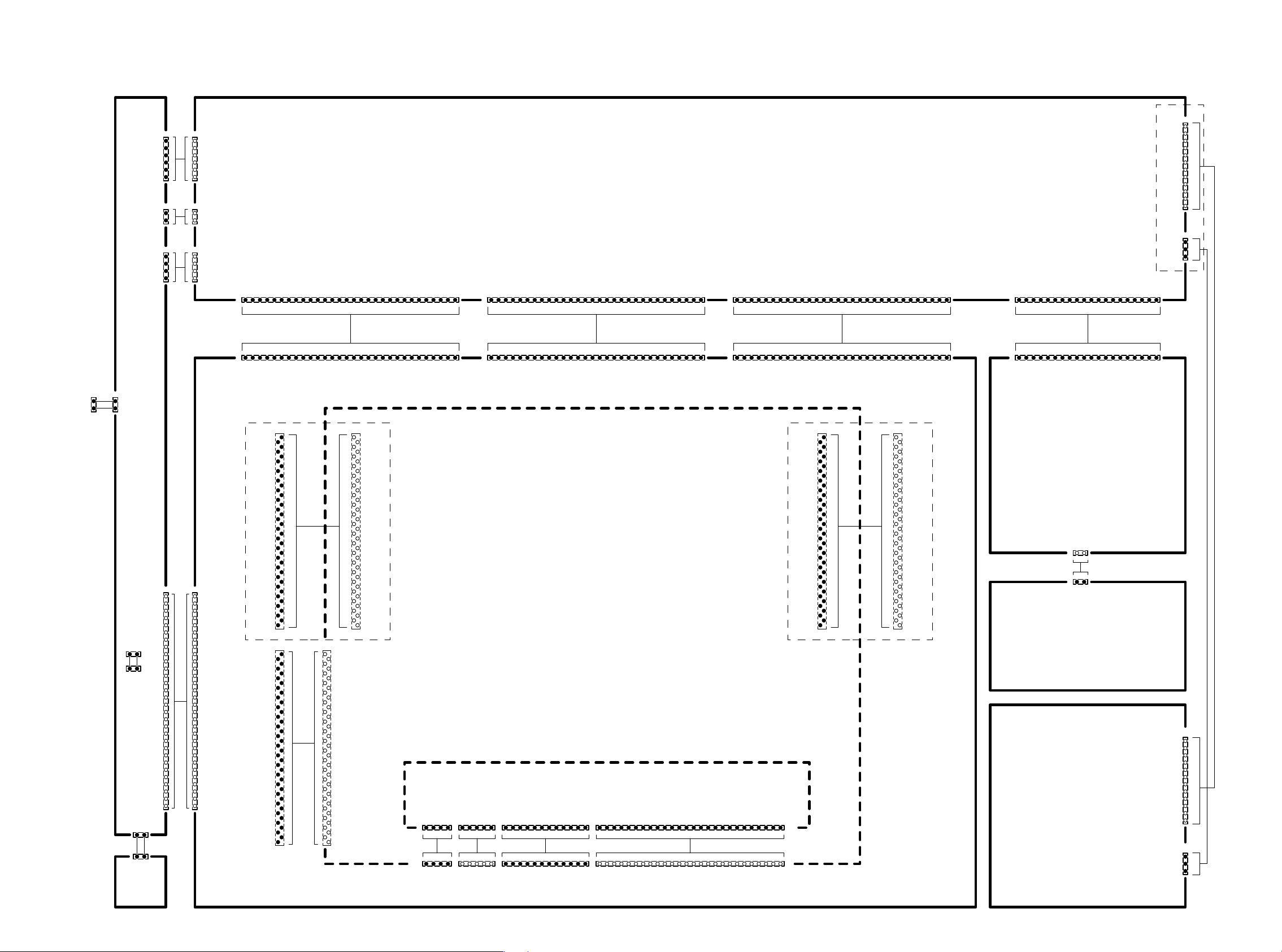
9. BLOCK DIAGRAM
DB-VLD302
LOADING MECHA BLOCK
PICK UP
SPDL-M
DISPLAY BLOCK (PF01)
KEY NETWORK
PLAY STOP PAUSE
OPEN/
PREV NEXT FL OFF
CLOSE
DB-VPB305
DVDM : DVD MECHA MODULE BLOCK
RF IC
LA9701M LC78652W
VF01
FL DISPLAY
RESET
IC
QF04
SERVO DSP
DVD DECODERFTS DRIVER
PE5220AM56788AFP
OF01
TMP87PM74F
MAIN CPU
SYSTEM CONTROL CPU
PD6345A
MPEG2 DECODER
M65774BFP
DVD AUDIO DSP
XCA56367PV150
OF08
EEP-ROM
IR
8MHz
SACD BLOCK
(PD01)
Q602
16M SDRAM
Q601
SACD
DECODER
ZF01
XF01
Q711
Q712
Q713
SELECTOR
VIDEO & AUDIO BLOCK (PM01)
V
Y
QA01
12BIT
VIDEO
ENCODER
QE01
PROGRESSIVE
HI-QUALITY
VIDEO
ENCODER
QE02
64M SDRAM
C
QA02
Y/G
QA03
CB/B
QA04
CR/R CR
N
QY01
Y
&
QB01
CB
QC01
CR
EXCEPT N
RA44 &
RY25
RA46 &
RB25
RA48 &
RC25
RA45
RA47
RA49
RY23
RB23
RC23
QV04
QV08
QV06
QD01
AUDIO DAC
QD21
AUDIO DAC
LPF
LPF
LPF
LPF
LPF
LPF
LPF
LPF
LPF
QV05
QV09
QV07
QY02
QB02
QC02
Q852
Q855
Q858
V
QV11
Y
VIDEO
AMP
V
JV01
COMPOSITE
V
Y
JV02
S1/S2
C
ASPECT
Y
QY04
VIDEO
CB
AMP
Q861
V
6dB
V
Q860
Y
6dB
Q853
G
6dB
Q856
B
6dB
C
Q859
R
6dB
L801
L802
L803
L804
L950
L951
RELAY
Y
CB
CR
Y
CB
CR
ASPECT
I/P
C
JY01
COMPONENT
JY02
D2
Terminal
for F,A,C,
L,S
J802
AUX-
SCART
J801
TV-
SCART
for N
J203
LPF
L/FL
HDAM
LPF
LPF
R/FL
J205
SURRL
HDAM
SURRR
LPF
WO01
SP01
POWER SUPPLY BLOCK
(PS01)
TP50
AUDIO TRANS.
LP01,CP01,CP02 DP01
AC LINE FILTER
DP50,DP51,DP52,DP53
CP50,CP51,QP55,QP63
RECTIFIERS &
RECTIFIER
QP01,QP02
SWITCHING
CIRCUIT
VOLTAGE REGULATORS
DP02,CP06,RP06,RP11
SNUBBER CIRCUIT
DP04,CP14,DP07,CP16,DP11,DP12,CP19,DP14
CP21,DP17,CP24,QP06,QP07,QP08
RECTIFIERS & VOLTAGE REGULATORS
TP01
SWITCHING TRANS
QP03
PHOTO CUPPLER
VOLTAGE
QP04
DETECTOR
STB_CTL
HEATERDC+3.5V-28VE+5VM+6VSW+5VSW+12VSW+3.3V+3.3VD+5VA+8VA -8VA
LPF
QD41
AUDIO DAC
HDAM
CENTER
SUB WOOFER
LPF
JI01
REMOTE
CONTROL
QI03
JI03
DIG OUT
COAX
JI04
DIG OUT
OPT
1413
Page 15
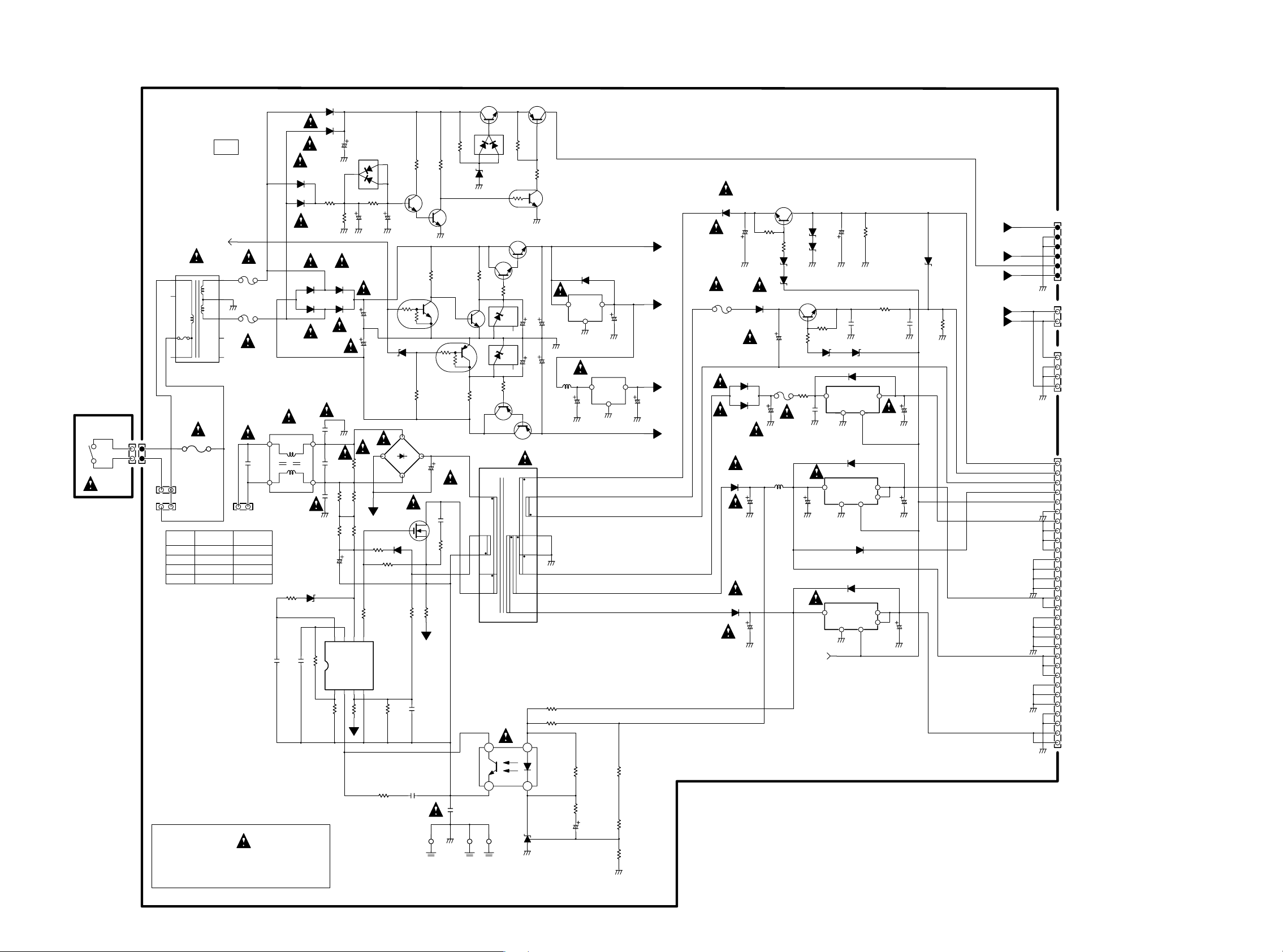
10. SCHEMATIC DIAGRAM
PS02
SP01
JP02JP08
2
1
1
2
PS01
LPS
DP56
1D3
DP57
1D3
STB_CTL
STB_CTL
TP50
1
2
3
4
12
JP03
NL
JP01
21
JP10 JP11
2121
NLNL
FP01 2A/125V T2AL/250V
CP03,04 470p/250V 220p/250V
CP05 220/200V 120/400V
RP01 2.2M/1/2W 1M/1W
NOTE ON SAFETY:
The parts marked with are important
parts on the safety.
Please use the parts having the designated parts
number without fail.
5
6
A-GND
7
8
9
FP01
JP04
F,L,U A,C,N,S
FP50
FP51
250VT500mA
250VT500mA
CP01
4
0.1/250v
1
CP08
0.33
LP01
LF-4D-223
RP08
10
CP09
0.22
DP52
1D3
DP53
1D3
DP03
22V
RP13
+7.3V
330k
DP54
1D3
DP55
1D3
RP56
1k
3
2
GND
RP14
+10.4V
CP57
DP62
2200/16V
1SS301
A-GND
2
RP58
3.3M
+6.7V
10k
CP58
RP57
GND
0.1/250V
RP02
RP05
QP02
FA3647
0.1/50V
CP50CP51
2200/16V
2200/16V
34
RP01
120K
120K
RP03
HOT
120K
RP06
68
RP07
RP09
47 1W
100
RP15
RP16
HOT
100
A-GND A-GND A-GND
DP50
1D3
DP51
1D3
CP02 CP03CP04
120K
RP04
CP07
22/50V
+14.2V
8765
1234
56k
31
QP56
2SC4081
+1.2V
2
B
CP59
+0.6V
10/50V
QP50
DTC114EU
2
DP58
3.9V
RP53
1
DP01
2
QP01
2SK2943
1
G
DP02
1SS254
10k
150
CP10
4700p
CP11RP17
0.1
RP60RP59
+2.4V
1
C
2
3
E
B
+0.6V
47k
S1WB(A)60
2
D
3
S
120k
RP10
HOT
EARTH
47k47k
+0V
1
C
2SC4081
3
E
A-GND
RP50
47k 15k
+0V
1
3
2
DTA114EU
CP05
CP06
RP11
RP12
0.22 2W
JP09
GND
22k
RP61
+5.4V
QP57
+8.8V
2
QP52
2SC4081
QP51
RP54
15k
150P 2kV
10 1W
CP12
220/250V
EARTH EARTH
QP58
2SC4081
+7.2V
CBE
+7.5V
2
31
DP63
1SS301
5.6V
DP64
A-GND
RP51
B
3
QP03
JP06 JP07
2
DTC114TUA
+10.0V
213
C
123
CBE
+8.8V
RP52
220
2
1
C
31
3
E
2
DP60
9.1V
31
1
-8.6V
RP55
220
-8.6V
B
C
123
-10.4V
TP01
1
2
3
4
5
6
41
PC123F2
32
QP04
TL431
QP60
QP53
2SD1762
B
QP61
2SC4081
DP59
9.1V
QP62
2SA1586
E
B
C
213
QP54
2SB1453
GND
QP59
2SA1586
3123
E
47k
RP62
A-GND
E
+8.2V
CP53 CP52
-8.0V
2
1
2
+7.5V
E
+5.2V
+4.2V
3
1
C
B
+7.4V
RP63
10k
+7.4V
1
3
CP54CP55
47/16V
220/16V220/16V
A-GND
47/16V
LP50
10
D-GND D-GND
7
9
8
10
11
GND
12
13
14
RP24
N.C.
RP18
470
RP19
1k
RP20
3.3k
CP13
1
50V
78M05
GND
A-GND
+5.0V
DP61
1D3
QP55
2
CP60
OUTIN
NJU7200L33
100/10V
D-GND
31
A-GND
QP63
GND
1
RP21
1k
RP22
5.6k
RP23
4.7k
OUTIN
GND
CP56
220/10V
+2.5V
+5.0V
32
+3.3V
CP61
47/10V
+8VA
+5VA
+3.3VD
-8VA
DP04
AG01
FP02
T250mA/250V
DP14
RK46
DP17
EK19
V: PLAY
CP14
DP11
RK33
DP12
RK33
-29.0V
47/50V
CP24
220/25V
GND
DP07
AG01
+4.7V
+6.1V
CP21
RP25
4.7k
-28.4V
-14.7V
CP16
T2.5A/250V
CP19
1000/16V
1000/10V
+12.7V
QP09
2SC1740
3
E
B
RP32
680
-14.0V
220/10V
FP03
LP03
47
24
2
DP20 DP19
1
C
DP05
9.1V 20V
QP05
2SC1627
1
C
RP28
RP33
0.47
+4.1V
GND
20V
GNDGND
2
B
330
2W
0.1
CP27
GND
CP22
STB_CTL
3
E
RP27
4.7k
470/10V
CP15
47/50V
DP06
9.1V
GND GND
-14.9V
GND
DP08 DP09
10V 5.1V
1
QP06
PQ3RF33
34
GND
DP15
1D3
5
QP07
SI-3050C
12
GNDGND
1SS254
DP18
1D3
5
QP08
SI-3120F
12
GND
STB_CTL
CP17
DP16
0.01
DP21
1D3
RP26
TO PM01
JP50
GND
JP05
1
2
3
4
5
6
1
2
1
2
3
4
30
29
28
27
26
25
24
23
22
21
20
19
18
17
16
15
14
13
12
11
10
9
8
7
6
5
4
3
2
1
+3.3VD
A-GND
A-GND
+5VA
P_MUTE
-8VA
JP51
-8VA
+8VA
JP52
+8VA
A-GND
A-GND
-8VA
TO PD01
SACD
-28V
DC+3.5V
HEATER
E+5V
STB_CTL
GND
SW+3.3V
SW+3.3V
SW+3.3V
SW+3.3V
GND
GND
GND
GND
SW+5V
SW+5V
GND
GND
GND
GND
M+6V
M+6V
M+6V
M-GND
M-GND
M-GND
GND
GND
SW+12V
SW+12V
AUDIO
+5VA
-8VA
-8VA
+8VA
+5.0V
+6.1V
+12.2V
-29.0V
-15.4V
-19.0V
+5.3V
+3.4V
+3.3V
+3.3V
+5.0V
-8.9V
-7.4V
A-GND
+7.5V
A-GND
GND
GND
GND
M-GND
10k
DP10
13V
RP29
3.3
0.01
CP18
GND
2
CP20
GNDGND
3
4
CP23
GND
3
4
CP25
100/16V
GND
RP31
GND
470/10V
220/10V
+3.3VD
10k
15 16
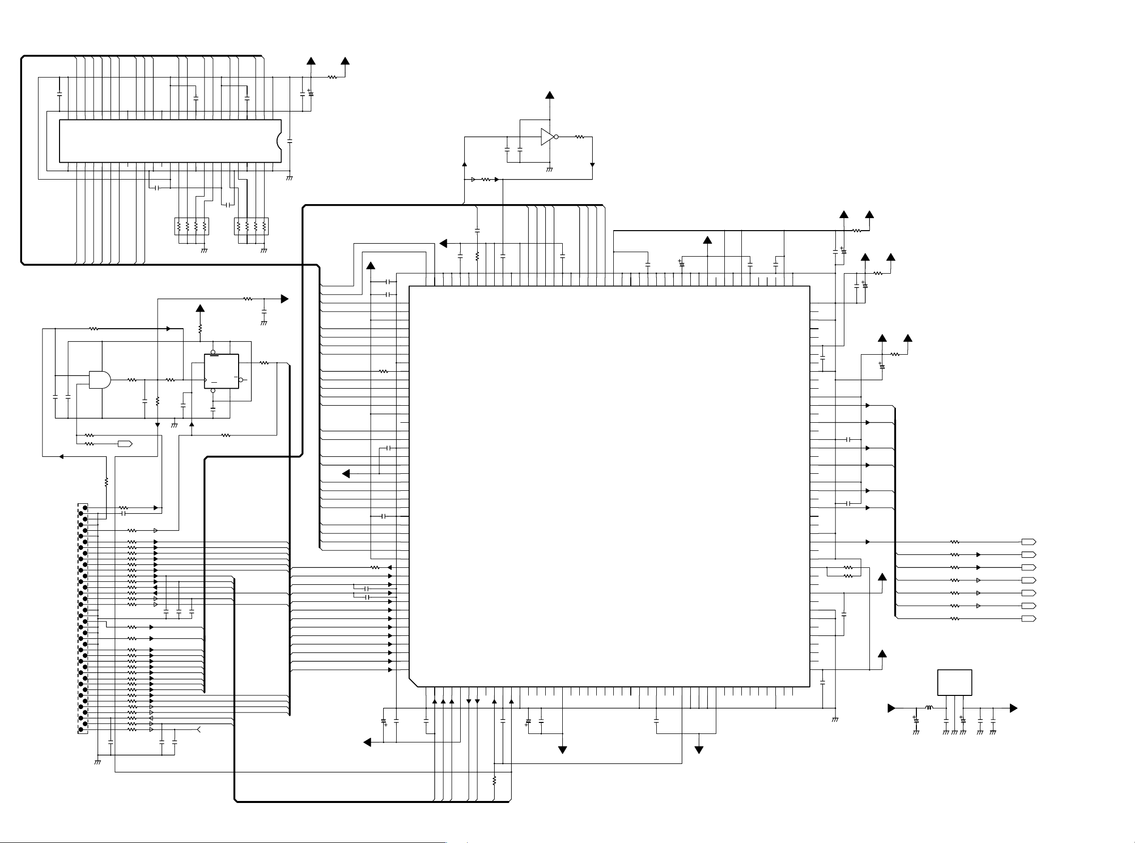
Page 16
A[0]
A[1]
A[2]
A[3]
0.47
C639
A2
A3
VCCVSS
A4A5A6A7A8A9NC
26 27 28 29 30 31 32 33 34 35 36 37 38 39 40 41 42 43 44 45 46 47 48 49 50
A[5]
A[4]
Q603
TS7SH08FU
2
1
1
N.C.
C642
C662
R614
R615
N.C.
FROM
XMSLAT2
GND
33MSACD
GND
BCLK
GND
XSAK
BD0
BD1
BD2
BD3
BD4
XDFSO
XDFSCK
XDFSI
XSRQ
XMSLAT
DSPA2
GND
GND
VCOSCD
GND
GND
RFSACD
GND
RD1
RD2
RD3
RD4
RD5
RD6
RD7
RD8
XSHD
BD7
BD6
BD5
XMRST
XSACDSL
J601
2
4
6
8
10
12
14
16
18
20
22
24
26
28
30
32
34
36
38
40
DVDM
XMSREADY
R613
N.C.
0
1
3
5
7
9
11
13
15
17
19
21
23
25
27
29
31
33
35
37
39
D-GND
A[6]
A1
R632
A0
A[7]
SACDSL
0
C659
A[11]
A[10]
A11
A10
A[9]
A[8]
5
4
3
R631
C654
N.C.
R633
R634
R635
R636
R637
R638
R639
R640
R641
R642
R643
R644
R645
R646
R647
R648
R649
R650
R651
R652
R653
R654
R655
R656
R657
R658
R659
R660
R661
R662
N.C.
22
XCS
R616
XRAS
DCKE
22
SACDSL
47
XWE
XCAS
XWE
XCAS
XRAS
CKE
C643
0
0
0
0
0
0
0
22
22
22
0
22
0
0
N.C.
N.C.
N.C.
N.C.
N.C.
N.C.
N.C.
N.C.
0
0
0
0
22
22
22
N.C.
VCCQ
LDQM
Q602
HY57V161610DTC-8
CLK
UDQMNCVCCQ
C640
0.47
R611 R612
10k 10k
x4 x4
DCLK
R618
0
0
R617
D-GND
N.C.
C657
C656
N.C.
C660
DQ[4]
DQ[5]
DQ[6]
DQ[7]
0.47
C638
DQ4
DQ5
DQ6
DQ7
VSSQ
DQ8
DQ9
VSSQ
DQ10
DQ11
1357
2 4 6 8
D-GND D-GND
SW+3.3V
+3.3V
R663
0
Q604
TC74VHC74FT
1
CLR
2
D
3
CLK
PR GND
4
N.C.
C645
N.C.
SACDSL
C661
N.C.
N.C.
C658
WCK
WAREFI
WAD[0]
WAD[1]
WAD[2]
WAD[3]
WAD[4]
WAD[5]
WAD[6]
WAD[7]
C646
MSDATAO
SACDSL
0.47
MSDATAI
XMSLAT1
MSREADY
VCCQ
VCCQ
C641
R621
N.C.
MSCK
XRST
DQ[3]
0.47
14
VCC
7
DQ[2]
0.47
C637
DQ2
DQ3
VSSQ
DQ12
DQ13
VSSQ
1357
2468
R619
0
C644
N.C.
5
Q
6
Q
DQ[1]
DQ1
DQ14
DQ[0]
DQ0
DQ15
D-GND
R620
22
12345678910111213141516171819202122232425
VCC
VSS
SDCK
XSAK
SD[0]
SD[1]
SD[2]
SD[3]
SD[4]
XSRQ
XSDEF
XSHD
SD[7]
SD[6]
SD[5]
D-GND
V+3_SDRAM SW+3.3V
R610
0.47
C634
C635
100/6.3V
0.47
C636
DQ[7]
33M
DQ[6]
DQ[5]
DQ[4]
DQ[3]
DQ[2]
DQ[1]
DQ[0]
DCLK
DCKE
XWE
XCAS
XRAS
A[11]
A[10]
A[9]
A[8]
A[7]
A[6]
A[5]
A[4]
A[3]
A[2]
A[1]
A[0]
XSRQ
XSHD
SDCK
XSAK
XSDEF
SD[0]
SD[1]
SD[2]
SD[3]
SD[4]
SD[5]
SD[6]
SD[7]
0
V+2C
+3.3V
V+2C
C632
C633
V+3IO
R609
47p
N.C.
PD01-1/2
C627
0.47
C628
N.C.
133
DQ5
134
DQ4
135
VDIO
136
DQ3
137
DQ2
138
DQ1
139
DQ0
140
22
C630
N.C.
VSIO
141
DCLK
142
DCKE
143
XWE
144
XCAS
145
XRAS
146
VDIO
147
TEST0
148
A11
149
A10
150
VSC
151
A9
152
A8
153
DVDC
154
A7
155
A6
156
A5
157
A4
158
VSIO
159
A3
160
A2
161
A1
162
A0
163
VDIO
164
VSRQ
165
VSHD
166
SDCK
167
XSAK
168
XSDEP
169
SD0
170
SD1
171
SD2
172
SD3
173
SD4
174
SD5
175
SD6
176
SD7
0.47
C602
R608
C631
22
C601
N.C.
100/6.3V
WCK
WAREFI
V+2C
132
131
130
DQ6
DQ7
VSIO
VSC
XMSLAT
MSCK
123456789
N.C.
C603
XMSLAT1
MSCK
129
MSDATAI
C626
WAVSS
MSDATI
0.47
47
R607
128
127
126
WARFI
WAVSS
WAVRB
VDC
MSDATO
MSREADY
MSREADY
MSDATAO
SW+3.3V
+3.3V
Q605
5
N.C.
R623
3
WAD5
LRCK
C606
WAD[4]
117
0.47
116
WAD4
FRAME
V+3IO
VSC
VDIO
+3.3V
C623
115
N.C.
0.47
VSIO
MNT0
WAD[3]
114
WAD3
MNT1
WAD[2]
113
WAD2
MNT2
WAD[0]
WAD[1]
112
111
WAD1
Q601
CXD2753R
MNT3
WAD0
TESTO
C622
0.47
110
109
108
107
VDIO
TESTI
TESTI
TESTI
TESTO
TESTO
TESTO
TCK
24
10p
N.C.
C648
C647
R622
0
C625
0.01
0.01
C624
125
124
123
122
WCK
TESTI
WAVDD
WAVDD
XMSDOE
XRST
SMUTE
MCKI
1011121314151617181920212223242526272829303132
N.C.
C604R601
0
MCK
XRST
D-GND
WAD[5]
WAD[6]
WAD[7]
121
120
119
118
VDC
WAD7
WAD6
VSIO
EXCKO1
EXCKO2
C605
100/6.3V
V+3IO SW+3.3V
R606
+3.3V
C618
C614
0.47
C608
D-GND
0.47
0.47
R603
C611
0.47
C610
0.47
R602
N.C
0
V+2C V+2V
C617
100/6.3V
0.47
C616
0
C609
0.47
R605
0
C615
100/6.3V
V+3DSD SW+3.3V
R604
0
C612
100/6.3V
DSARS
DSALS
DSALFE
DSAC
DSAR
DSAL
DSAC
DSALFE
V+2C
DSALS
DSARS
DSAL
DSAR
V+3IO
+3.3V
+3.3V
SW+3.3V
+3.3V
R624
22
R625
22
R626
22
R627
22
R628
22
R629
22
R630
22
Q606
BA25BC0FP
123
L601
0
0.47
C649
C650
100/6.3V
D-GND D-GND D-GNDD-GND D-GND
D-GND
C651
100/6.3V
C652
0.47
DSDCLK
DSD-SW
DSD-LS
DSD-RS
0.47
C653
DSD-C
DSD-L
DSD-R
DSDCLK
DSD-C
DSD-SW
DSD-LS
DSD-RS
DSD-L
DSD-R
V+2V
V+2C
C621
100/6.3V
106
105
104
103
VSIO
TESTI
TESTI
TESTI
TDI
VSC
TDO
TMS
C607
0.47
9998979695949392919089
102
101
100
VDC
TESTI
TESTI
TRST
TESTI
TEST1
V+2C
TESTI
TESTO
TEST2
TEST3
VDC
TESTO
3334353637383940414243
TESTI
XBIT
VSC
TESTI
SUPDT0
SUPDT1
C620
0.47
C619
TESTO
TESTO
SUPDT2
SUPDT3
0.47
TESTO
VSIO
VDIO
VDDSD
DSALFE
ZDFLFE
VDDSD
PHREFO
PHREFI
BCKAO
BCKASL
XSUPAK
SUPDT7
SUPDT6
SUPDT4
44
TESTI
TESTI
TESTO
VSIO
TESTO
TESTO
VDC
TESTO
TESTO
VSC
TESTO
TESTO
DSARS
ZDFRS
DSALS
ZDFLS
VSDSD
DSAC
ZDFC
DSAR
ZDFR
DSAL
ZDFL
BCKAI
VSDSD
TESTO
TESTO
TESTO
TESTO
TESTI
TESTI
TESTO
VSC
VDIO
SUPDT5
88
87
86
85
84
83
82
81
80
79
78
77
76
75
74
73
72
71
70
69
68
67
66
65
64
63
62
61
60
59
58
57
56
55
54
53
52
51
50
49
48
47
46
45
1817
Page 17
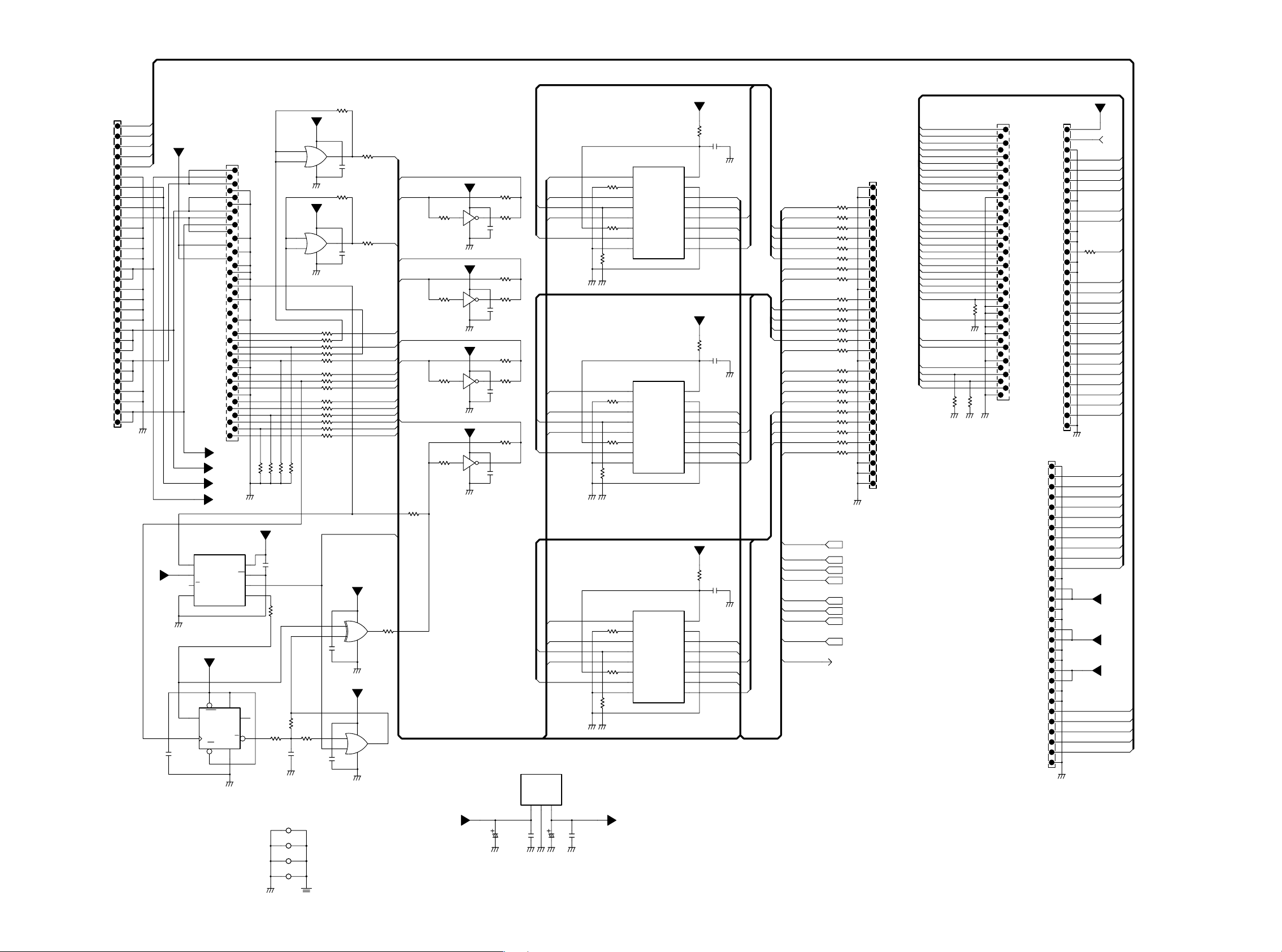
FROM PS01
-28V
DC+3.5V
HEATER
E+5V
STBCTL
GND
SW+3.3V
SW+3.3V
SW+3.3V
SW+3.3V
GND
GND
GND
GND
SW+5V
SW+5V
GND
GND
GND
GND
M+6V
M+6V
M+6V
MGND
MGND
MGND
GMD
GND
SW+12V
SW+12V
10
11
12
13
14
15
16
17
18
19
J701
21
22
23
24
25
26
27
28
29
30
1
2
3
4
5
6
7
8
9
20
-28V
DC+3.5V
HEATER
E+5V
STBCTL
D-GND
33M
C704
0.1
PD01-2/2
SW+2.5V
+3.3V
+5.0V
D-GND
TC7WH74FU
+12.2V
+6.1V
1
2
3
4
2
1
Q704
FROM MECHA
MGND
SW+5V
MGND
GND
M+6V
GND
M+6V
SW+3.3V
12V
SW+3.3V
GND
SW+2.5V
GND
SW+2.5V
GND
GND
GND
DACCLK
NC
GND
NC
XCSAQE
GND
XAQRST
D_OUT
XDFSO
XAMYTE
XDFSCK
XMMUTE
GND
DATA1
BCK
DATA2
GND
XCSDF1
DATA0
XFRST1
LRCK
XFRST0
XCSDF0
M+6V
SW+3.3V
SW+5V
Q703
TC7WH157FU
A
B
Y
GND
SW+3.3V
+3.3V
8
CLR
D
CLK
PR GND
7
2
4
6
8
10
12
14
16
18
20
22
24
26
28
30
32
34
36
38
40
SW+12V
6
VCC
4
D-GND
J702
VCC
SEL
Q
Q
1
3
5
7
9
11
13
15
17
19
21
23
25
27
29
31
33
35
37
39
D-GND
ST
Y
5
3
+3.3V
8
7
6
5
10k
R715
SW+3.3V
10k
R716
C703
R724
10k
0.1
R723
R725
10k
R717
22
33k
Q701
TC7SH32FU
1
2
Q702
TC7SH32FU
1
2
10k
R718
R726
0
C705
0.1
D-GND
SW+3.3V
5
3
D-GND
SW+3.3V
5
3
D-GND
R701
R702
R703
R704
R705
R706
R707
R708
R709
R710
R711
R712
R713
R714
C707
0.1
VDD
XST
VDD
XST
VDD
XST
4A
4B
4Y
3A
3B
3Y
+3.3V
4A
4B
4Y
3A
3B
3Y
+3.3V
4A
4B
4Y
3A
3B
3Y
R741
+3.3V
R745
R749
SW+3.3V
0
16
15
14
13
12
11
10
9
SW+3.3V
0
16
15
14
13
12
11
10
9
SW+3.3V
0
16
15
14
13
12
11
10
9
C712
0.1
D-GND
DSD-L
DATA0/DSD-L
BCK
DSD-R
BCK/DSD-R
C713
0.1
D-GND
DATA1
DSD-LS
DATA1/DSD-LS
BCK
DSD-RS
BCK/DSD-RS
C714
0.1
D-GND
DSD-C
DATA2/DSD-C
BCK
DSD-SW
BCK/DSD-SW
XCSDF0
MCLK1
DSDCLKOUT1
LRCKOUT1
BCK/DSD-R
DATA0/DSD-L
XFRST0
XAMUTE
MCLK2
DSDCLKOUT2
LRCKOUT2
BCK/DSD-RS
DATA1/DSD-LS
XMMUTE
XCSDF1
XDFSO
XDFSCK
MCLK3
DSDCLKOUT3
LRCKOUT3
BCK/DSD-SW
DATA2/DSD-C
XFRST1
SACDSL
DSDCLK
DSD-C
DSD-SW
DSD-LS
DSD-RS
DSD-L
DSD-R
D_OUT
TO PM01 AUDIO
30
29
0
R756
R757
R758
R759
R760
R761
R762
R763
R764
R765
R766
R767
R768
R769
R770
R771
R772
R773
R774
R775
R776
R777
R778
D_OUT
0
0
0
0
0
0
0
0
0
0
0
0
0
0
0
0
0
0
0
0
0
0
D-GND
SACDSL
DSDCLK
DSD-C
DSD-SW
DSD-LS
DSD-RS
DSD-L
DSD-R
28
27
26
25
24
23
22
21
20
19
18
17
16
15
14
13
12
11
10
J703
9
8
7
6
5
4
3
2
1
GND
GND
XCSDF0
MCLK1
DSDCLKOUT1
LRCKOUT1
BCK/DSD-R
DATA0/DSD-L
XFRST0
XAMUTE
GND
MCLK2
DSDCLKOUT2
LRCKOUT2
BCK/DSD-RS
DATA1/DSD-LS
XMMUTE
GND
XCSDF1
XDFS0
XDFSCK
MCLK3
DSDCLKOUT3
LRCKOUT3
BCK/DSD-SW
DATA2/DSD-C
XFRST1
GND
GND
GND
LT1
XRESET
TXD
S(M-TO-F)
RXD
S(F-TO-M)
DTR
SSCK
CTS
XREADY
VQESCK
VQESSO
XCSPRO2
PD[7]
PD[6]
PD[5]
PD[4]
PD[3]
PD[2]
PD[1]
PD[0]
HSYNC
VSYNC
XVQERST
AV1CLK
SCL0
SDA0
VSEL1
LETTER
SQUEEZE
VSEL2
R753
D-GND
10k
10k
R755
R754
D-GND D-GND
FROM DVDM
J704
2
4
6
8
10
12
14
16
18
20
22
24
26
28
10k
30
32
34
36
38
40
D-GND
1
LT1
XRESET
3
TXD
S(M-TO-F)
5
RXD
S(F-TO-M)
7
DTR
SSCK
9
CTS
XREADY
11
GND
13
VQESCK
VQESSO
15
XCSPRO2
PD[7]
17
PD[6]
PD[5]
19
PD[4]
PD[3]
21
PD[2]
PD[1]
23
PD[0]
HSYNC
25
VSYNC
XVQERST
27
GND
GND
29
AV1CLK
GND
31
GND
SCL0
33
SDA0
35
GND
VSEL1
37
LETTER
SQUEEZE
39
VSEL2
GND
SW+12V
SW+12V
TO PM01
MAIN
10
11
12
13
14
15
16
17
18
19
J706
1
2
3
4
5
6
7
8
9
20
21
22
23
24
25
26
27
28
29
30
TO PM01
MAIN
10
11
12
13
14
15
16
17
18
19
20
21
22
23
24
25
26
27
28
29
30
D-GND
R719
N.C
R720
0
0
0
0
0
0
0
0
0
0
0
0
0
0
R721
N.C
+3.3V
1
2
C706
1
2
C701
0.1
C702
0.1
SW+3.3V
0.1
SW+3.3V
5
3
D-GND
5
3
D-GND
+3.3V
22
XDFSO
R722
22
XDFSCK
D_OUT
XAMUTE
XMMUTE
DATA1
DATA2
XCSDF1
DATA0
XFRST1
LRCK
XFRST0
XCSDF0
SACDSL
Q705
TC7SH86FU
4
4
Q706
TC7SH32FU
BCK
R727
Q711
TC74VHC157FT
MCLK1
DACCLK
MCLK2
DACCLK
MCLK3
DACCLK
DACCLK
R728
N.C.
22
+3.3V
R732
22
2
Q708
TC7SHU04FU
+3.3V
R735
22
Q709
TC7SHU04FU
+3.3V
R738
22
254
Q710
TC7SHU04FU
+3.3V
R729
N.C.
254
Q707
N.C.
SW+3.3V
5
3
D-GND
SW+3.3V
254
3
D-GND
SW+3.3V
3
D-GND
SW+3.3V
3
D-GND
R733
N.C
R734
22
4
C709
0.1
R736
N.C.
R737
22
C710
0.1
R739
N.C.
R740
22
C711
0.1
R730
0
C708
N.C.
SACDSL
DSDCLK DATA0
DSDCLKOUT1
LRCK
LRCKOUT1
D-GND
SACDSL
DSDCLK
DSDCLKOUT2
LRCK
LRCKOUT2
D-GND
SACDSL
DSDCLK DATA2
DSDCLKOUT3
LRCK
LRCKOUT3
D-GND
Q714
BA25BC0FP
R742
R744
D-GND
R748
D-GND
R752
D-GND
R743
10k
R746
R747
10k
R750
R751
10k
0
0
0
0
0
0
1
SELECT
2
1A
3
1B
4
1Y
5
2A
6
2B
7
2Y
8
GND
TC74VHC157FT
1
SELECT
2
1A
3
1B
4
1Y
5
2A
6
2B
7
2Y
8
GND
TC74VHC157FT
1
SELECT
2
1A
3
1B
4
1Y
5
2A
6
2B
7
2Y
8
GND
Q712
Q713
4
4
SW+5V
J705
1
+5.0V
2
D_OUT
+12.2V
+6.1V
+3.3V
+3.4V
+5.3V
-19.0V
-15.4V
-29.0V
R731
0
D_OUT
VSEL2
SQUEEZE
LETTER
VSEL1
SDA0
SCL0
AV1CLK
XVQERST
VSYNC
HSYNC
PD[0]
PD[1]
PD[2]
PD[3]
PD[4]
PD[5]
PD[6]
PD[7]
XCSPRO2
VQESSO
VQESCK
CTS
DTR
RXD
TXD
XREADY
SSCK
S(F-TO-M)
S(M-TO-F)
XRESET
LT1
SW+12V
M+6V
SW+3.3V
STBCTL
E+5V
HEATER
DC+3.5V
-28V
3
4
5
6
7
8
9
D-GND
J707
J708
J709
J710
D-GND EARTH
SW+3.3V
+3.3V
0.47
C715
C716
100/6.3V
D-GND D-GND
D-GND
D-GND
C717
100/6.3V
D-GND
C718
0.47
SW+2.5V
123
19 20
Page 18
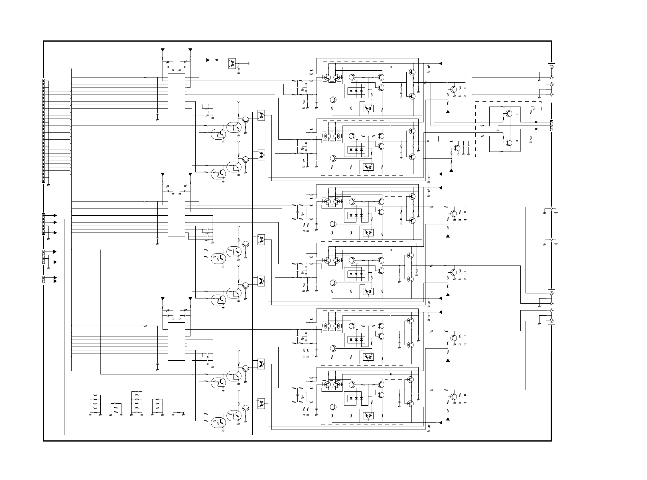
FROM
PD01
FROM
PS01
-8VDA
PMUTE
+5VDA
DAC-GND
DAC-GND
+3.3VDD
PM01-1/5
J201
30
29
28
27
26
25
24
23
22
21
20
19
18
17
16
15
14
13
12
11
10
9
8
7
6
5
4
3
2
1
DAC-GND
J202
6
-7.4V
5
-8.9V
4
+5.0V
3
2
+3.3V
1
DAC-GND
J207
-7.4V
4
-8VA
3
GND
2
GND
+7.5V
1
+8VA
GND
J208
+7.5V
2
+8VA
-7.4V
1
-8VA
DATA2/DSD-C
BCK/DSD-SW
LRCKOUT3
DSDCLKOUT3
XMMUTE
DATA1/DSD-LS
BCK/DSD-RS
LRCKOUT2
DSDCLKOUT2
XAMUTE
DATA0/DSD-L
BCK/DSD-R
LRCKOUT1
DSDCLKOUT1
-8VDA
+5VDA
+3.3VDD
-8VA
+8VA
+8VAA
-8VAA
XFRST1
MCLK3
XDFSCK
XDFSO
XCSDF1
MCLK2
XFRST0
MCLK1
XCSDF0
XFRST0
DATA0/DSD-L
BCK/DSD-R
LRCKOUT1
MCLK1
DSDCLKOUT1
XDFSCK
XDFSO
XCSDF0
XAMUTE
XFRST1
DATA1/DSD-LS
BCK/DSD-RS
LRCKOUT2
MCLK2
DSDCLKOUT2
XDFSCK
XDFSO
XCSDF1
XMMUTE
XFRST1
DATA2/DSD-C
BCK/DSD-SW
LRCKOUT3
MCLK3
DSDCLKOUT3
XDFSCK
XDFSO
XCSDF1
+3.3VDD +5VDA
A-GND
AMUTEC
AOUTA-
AOUTA+
AGND
AOUTB+
AOUTB-
BMUTEC
CMOUT
A-GND
AMUTEC
AOUTA-
AOUTA+
AGND
AOUTB+
AOUTB-
BMUTEC
CMOUT
A-GND
AMUTEC
AOUTA-
AOUTA+
AGND
AOUTB+
AOUTB-
BMUTEC
CMOUT
NC
FILT+
FILT+
FILT+
CD08
VA
CD27
100/10V
CD28
VA
CD47
100/10V
CD48
VA
+5.0V
0
SW+12V
RD11
1
20
19
18
17
16
15
14
13
12
11
+5VDA+3.3VDD
1
20
19
18
17
16
15
14
13
12
11
+5VDA
1
20
19
18
17
16
15
14
13
12
11
+5.0V
CD06
0.1
CD03
1/50V
A-GND
R225
1k
R226
1k
2
+0V
DTC114EUA
R255
1k
R256
1k
2
+0V
DTC114EUA
0
RD31
CD26
0.1
CD23
1/50v
A-GND
R425
1k
R426
1k
2
+0V
DTC114EUA
R455
1k
R456
1k
2
+0V
0
RD51
DTC114EUA
CD46
0.1
CD43
1/50v
A-GND
R525
1k
R526
1k
2
+0V
DTC114EUA
R555
1k
R556
1k
2
+0V
Q537
DTC114EUA
BLM11B601S
LD01
CD05
1/50V
CD04
0.1
+2.9V
Q207
+2.9V
Q237
CD25
1/50v
CD24
0.1
+2.9V
Q407
Q437
CD45
1/50v
CD44
0.1
Q507
+2.9V
+2.9V
+2.9V
A-GND
A-GND
A-GND
A-GND
A-GND
A-GND
2
1
3
2
1
3
2
1
DTC114EUA
3
2
1
DTC114EUA
3
2
1
3
2
1
DTC114EUA
3
D200
1SS301
3
1
Q208
DTC114EUA
Q238
DTC114EUA
Q408
Q438
+0V
Q508
DTC114EUA
Q538
+11.5V
2
DAC-GND
MUTE+12V
3.3k
R227
+0V
A-GND
MUTE+12V
3.3k
R257
+0V
A-GND
MUTE+12V
3.3k
R427
+0V
A-GND
MUTE+12V
3.3k
R457
+0V
A-GND
MUTE+12V
3.3k
R527
A-GND
MUTE+12V
3.3k
R557
+0V
A-GND
1
3
1
3
1
3
1
3
1
3
1
3
C200
100/16v
2SA1586
E
2SA1586
E
2SA1586
E
2SA1586
E
2SA1586
E
2SA1586
E
Q209
A-GND
Q239
A-GND
Q409
A-GND
Q439
A-GND
Q509
A-GND
Q539
A-GND
B
B
B
B
B
B
MUTE+12V
C
10k
R228R258
C
10k
123
C
123
C
10k
123
C
10k10k 10k
R528R558 R428R458
123
C
A-GND
J203
1
L
3
2
A-GND
A-GND
F221
0
F251
0
R
4
FL
6
5
FR
J204
1
2
3
N only
J206
EARTHA-GND
J209
EARTH
DAC-GND
J205
4
SL
6
5
A-GND
A-GND
SR
1
C
3
2
SW
+8VA
C211
220/16V
A-GND
C241
220/16V
220/16V
A-GND
A-GND
C411
220/16V
C441
220/16v
A-GND
A-GND
C511
220/16V
C541
220/16V
A-GND
+7.5V
C210
220/16V
Q204
R215
2SC4213
220
E
3
22k
C212
270p
R216
B
2
C
1
2.2k
R219
A-GNDA-GNDA-GND
220k
R217
-7.4V
-8VDA
R220
A-GND
22k
R246
A-GND
C542
R250
270p
C242
270p
C412
270p
C442
270p
C512
270p
R245
Q234
2SC4213
220
E
3
B
2
C
1
2.2k
R249
A-GNDA-GND
220k
R247
-7.4V
C240
+7.5V
C410
220/16V
-7.4V
C440
220/16v
+7.5V
C510
220/16V
+7.5V
C540
220/16V
-7.4V
-8VDA
-8VA
+8VAA
Q404
R415
220
2SC4213
E
3
22k
B
2
R416
C
1
2.2k
R419
R417
R445
220
R449
R447
-8VAA
+8VAA
R515
220
R519
220k
R517
R545
220
R549
R547
-8VAA
220k
-8VDA
2.2k
220k
-8VDA
2.2k
-8VDA
2.2k
220k
-8VDA
B
B
B
-7.4V
-7.4V
-7.4V
2
2
2
-7.4V
A-GND
Q434
2SC4213
E
C
A-GND
Q504
2SC4213
E
C
A-GND
Q534
2SC4213
E
C
A-GND
A-GND
A-GND
3
22k
R446
1
A-GND
A-GND
3
22k
R516
1
A-GND
A-GND
3
22k
R546
1
A-GND
R221
220
Q206
E
3
2SC4213
B
2
C
1
2.2k
R224
0
A-GND
0
R254
R251
220
2.2k
Q236
2SC4213
C
1
2
B
E
3
22k22k
R222R252
270p270p
C221C251
A-GND
12k
R207
R208
R203 R205
2.2k 2.2k
C204
1000p
C205
1000p
A-GND
R206
12K
R209
A-GNDA-GND
R237
R238
R233
2.2k
C234
1000p
C235
1000p
A-GND
R236
R234R232
2.2k3.3k
12K
R239
A-GNDA-GND
R407
R408
R403
2.2k
C404
1000p
C405
1000p
A-GND
R406
R404
2.2k
12K
R409
A-GNDA-GND
R437
R438
R433
2.2k
C434
1000p
C435
1000p
A-GND
R436
R434
2.2k
12K
R439
A-GNDA-GND
R507
R508
R503
2.2k
C504
1000p
C505
1000p
A-GND
R506
R504
2.2k
12K
R509
A-GNDA-GND
R537
R538
R533
2.2k
C534
1000p
C535
1000p
A-GND
R536
R534
2.2k
12K
R539
A-GNDA-GND
15k
2.2k
15K
R210
C206
A-GND
12k
15k
R235
2.2k
2.2k
15K
C236
R240
A-GND
12k
15k
R405
2.2k
2.2k
C406
15K
R410
A-GND
12k
15k
R435
2.2k
2.2k
15K
C436
R440
A-GND
12k
15k
R505
2.2k
2.2k
15K15K
C506
R510R540
A-GND
12k
15k
R535
2.2k
2.2k
C536
A-GND
R201
3.3k
C203
100p
R202 R204
3.3k 2.2k
D221
1SS301
3
-7.2V
12123
-8.9V
R231
3.3k
D251
1SS301
3
-7.2V
12123
-8.9V
D421
1SS301
3
-7.2V
2
1
-8.9V
D451
1SS301
3
-7.2V
2
1
-8.9V
D521
1SS301
3
-7.2V
2
1
-8.9V
D551
1SS301
3
2
1
-8.9V
-7.2V
C233
100p
R401
3.3k
C403
100p
R402
3.3k
R431
3.3k
C433
100p
R432
3.3k
R501
3.3k
C503
100p
R502
3.3k
R531
3.3k
C533
100p
R532
3.3k
150
150
R302
R301
7
1
D
D
2
G
4
S
3
Q301
2SK389
C
1
220P
E
3
100
R303
150
R311
R312
1
D
D
2
G
4
S
3
2SK389
C
1
220P
E
3
100
R313
150
R321
R322
1
D
D
2
G
4
S
3
C
1
220P
E
3
150
R332
R331
1
D
D
2
G
4
S
3
2SK389
C
1
220P
E
3
150
R342
R341
1
D
D
2
G
4
S
3
Q341
C
1
220P
E
3
150
R351
R352
1
D
D
2
G
4
S
3
C
1
220P
E
3
E
3
R304
100
2
6
B
G
Q304
2SA1312
S
C
1
5
456
D301
Q303
2SC2873
+8VA
150
7
S
5
Q311
Q313
2SC2873
150
7
S
5
Q321
2SK389
Q323
2SC2873
100
R323
150
7
S
5
Q331
Q333
2SC2873
100
R333
150
7
S
5
2SK389
Q343
2SC2873
100
R343
150
7
S
5
Q351
2SK389
Q353
2SC2873
100
R353
IMN10
2
B
6
G
2SA1312
D311
2
B
6
G
2SA1312
D321
2
B
6
G
2SA1312
D331
2
B
6
G
2SA1312
2
B
2SA1312
6
G
D351 D341
2
B
123
560
R307
EG
3
R314
100
2
Q314
B
C
1
456
IMN10
123
560
R317
E
3
R324
100
2
Q324
B
C
1
456
IMN10
123
560
R327
E
3
R334
100
2
B
Q334
C
1
456
IMN10
123
560
R337
EG
3
R344
100
2
Q344
B
C
1
456
IMN10
123
560
R347
3
E
Q354
IMN10
2
B
C
1
456
560
R357
R354
100
123
EG
3
R305
100
Q305
2
2SA1312
B
1
C
C
1
2
Q306
2SC3324
B
E
3
33k
R306
31
560
R308
D302
2
1SS302
E
3
R315
Q315
100
2SA1312
2
B
C
1
C
1
Q316
2
2SC3324
B
E
3
33k
R316
31
560
R318
D312
2
1SS302
E
3
R325
100
Q325
2
2SA1312
B
1
C
C
1
2
Q326
2SC3324
B
E
3
33k
R326
31
560
R328
D322
2
1SS302
E
3
R335
100
Q335
2
2SA1312
B
1
C
C
1
Q336
2SC3324
2
B
E
3
33k
R336
31
560
R338
D332
2
1SS302
E
3
R345
Q345
100
2SA1312
2
B
1
C
C
1
Q346
2
2SC3324
B
E
3
33k
R346
31
560
R348
D342
2
1SS302
E
3
R355
Q355
100
2
2SA1312
B
1
C
C
1
Q356
2
2SC3324
B
E
3
33k
R356
31
560
R358
D352
2
1SS302
Q201
D
C301
A-GND
100
33p
A-GND
100
33p
A-GND
R359
33p
A-GND
3
2SK170
1
S
2
10
R211
10
100k
2SJ74
Q432
2SJ74
Q502
R213
R212
2SJ74
2
S
Q202
A-GND
G
1
3
D
D
3
1
S
2
10
R241
10
R242
100k
R243
2SJ74
A-GND
2
S
Q232
G
1
3
D
D
3
1
G
S
2
10
R411
10
100k
R412
R413
2
S
A-GND
G
1
Q402
2SJ74
3
D
D
3
1
G
S
2
10
R441
10
100k
R443
R442
2
S
A-GND
G
1
3
D
D
3
1
S
2
10
R511
10
R512
100k
R513
2
S
A-GND
G
1
3
D
D
3
1
G
S
2
10
R541
10
100k
R542
R543
2
S
A-GND
G
1
Q532
3
D
2SJ74
100
R309
33p
Q231
2SK170
100
R319
33p
C311
A-GND
Q401
2SK170
100
R329
33p
C321
A-GND
Q431
2SK170
Q501
2SK170
Q531
2SK170
100
C208
220P
C238
220P
C408
220P
C438
220P
R339
C331
C508
220P
R349
C341
C538
220P
C351
+3.3V
CD01 CD07
0
220/16V 100/10V
RD01
CD02
0.1
RD02
0
RD22
0
RD42
0
NC
NC
RD04
NC
RD24
RD44
RD45
RD46
RD03
NC
RD23
NC
RD43
NC
R261
NC
R262
NC
R461
0
0
0
A-GNDDAC-GND
NC
R462
NC
R561
NC
R562
DAC-GND
1
XRESET
2
VL
3
SDATA
4
SCLK
5
LRCK
6
MCLK
7
M3
8
SCL/CCLK
9
M1
10
AD0/XCS
QD01
CS4392
N.C.N.C.N.C.
CD09CD29CD49
DAC-GND
+3.3V +5.0V
CD21
0
220/16V
RD21
CD22
0.1
DAC-GND
1
XRESET
2
VL
3
SDATA
4
SCLK
5
LRCK
6
MCLK
7
M3
8
SCL/CCLK
9
M1
10
AD0/XCS
QD21
CS4392
DAC-GND
+3.3VDD
+3.3V
CD41
0
220/16V
RD41
CD42
0.1
DAC-GND
1
XRESET
2
VL
3
SDATA
4
SCLK
5
LRCK
6
MCLK
7
M3
8
SCL/CCLK
9
M1
10
AD0/XCS
QD41
CS4392
DAC-GND
NC
R263
NC
R264
NC
R463
NC
R563
GNDDAC-GND DAC-GND A-GND A-GND A-GND D-GND A-GND
R265
2221
Page 19
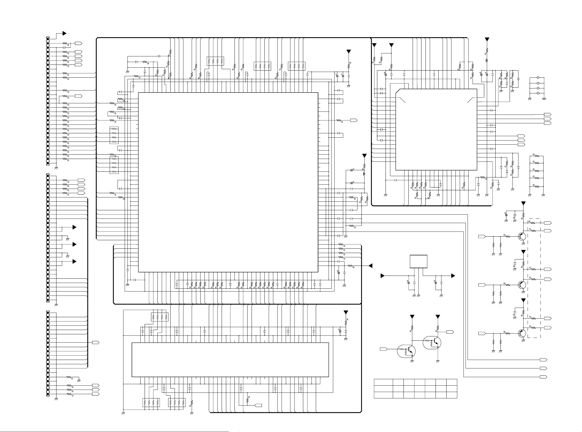
FROM
PD01
SW+5V
D_OUT
D-GND
VSEL2
SQUEEZE
LETTER
VSEL1
D-GND
SDA0
SCL0
D-GND
D-GND
AV1CLK
D-GND
D-GND
XVQERST
VSYNC
HSYNC
XCSPRO2
VQESSO
VQESCK
D-GND
FROM
PD01
D-GND
XREADY
SSCK
S(FtoM)
S(MtoF)
XRESET
D-GND
SW+12V
SW+12V
V-GND
V-GND
E+6V
E+6V
V-GND
V-GND
SW+3.3V
SW+3.3V
D-GND
D-GND
STB_CTL
E+5V
HEATER
DC+3.5V
D-GND
FROM
PD01
D-GND
DC+3.5V
HEATER
E+5V
STB_CTL
D-GND
P_TRG
XRESET
S(MtoF)
S(FtoM)
SSCK
XREADY
D-GND
/TEST
D-GND
IR_SW
D-BUS
V-MUTE
DTR
RXD
TXD
-28V
-28V
PD0
PD1
PD2
PD3
PD4
PD5
PD6
PD7
CTS
+5.0V
D-GND
D-GND
CE01
RE01
RE02
RE03
RE04
RE05
RE06
RE07
RE08
RE84
RE09
RE10
RE11
RE12
RE13
RE14
RE15
RE16
RE17
RE18
RE19
RE20
RE21
RE22
RE23
RE24
RE25
RE26
+12.2V
-29.0V
-15.4V
-19.0V
+5.3V
+3.4V
+6.1V
+3.3V
RE36
RE27
RE28
RE29
SW+5V
0
N.C.
0
0
0
0
0
0
0
0
0
0
0
22
22
22
22
22
22
22
22
0
0
0
0
0
0
0
V-GND
V-GND
N.C.
D_OUT
VSEL2
SQUEEZE
LETTER
VSEL1
AV1CLK
CKE
XVQERST
VSYNC
HSYNC
XCSPRO2
VQESSO
VQESCK
CTS
DTR
RXD
TXD
XREADY
SSCK
S(FtoM)
S(MtoF)
XRESET
LT1
SW+12V
E+6V
+3VD
STB_CTL
E+5V
HEATER
DC+3.5V
-28V
-28V
DC+3.5V
HEATER
E+5V
STB_CTL
LT1
XRESET
S(MtoF)
S(FtoM)
SSCK
XREADY
D-GND
0
0
0
JE01
30
29
28
27
26
25
24
23
22
21
20
19
18
17
16
15
14
13
12
11
10
9
8
7
6
5
4
3
2
1
JE02
30
29
28
27
26
25
24
23
22
21
20
LT1
19
18
17
16
15
14
13
12
11
10
9
8
7
6
5
4
3
2
1
JE03
20
19
18
17
16
15
14
13
12
LT1
11
10
9
8
7
6
5
4
3
2
1
D-GND
PM01-2/5
SDA0
SCL0
AV1CLK
RE31
PR2CLK
PPD0
PPD1
PPD2
PPD3
PPD4
PPD5
PPD6
PPD7
HSYNC
VSYNC
PD0
PD1
PD2
PD3
PD4
PD5
PD6
PD7
P_TRG
IR_SW
D-BUS
V-MUTE
RE33
RE34
RE38
RE39
RE43
PD0
PD1
PD2
PD3
PD4
PD5
PD6
PD7
RE35
7531
7531
CE04
0
0
CE03
0
0
0RX4
0
MA4
MA3
MA5
MA2
RE30
RE32
0RX4
RE44
CE02
0.1
0.1
CE05
0.1
0
0
8642
0.1
8642
0
D-GND
D-GND
D-GND
PC5
PC4
PC6
2468
1357
CE33
0.1
144
145
146
PC4
PC5
VDD3
PC3
PC2
PC1
PC0
PB8
PB9
PB5
PB6
PB7
2468
0
0
RE60
RE62
140
141
142
143
GND
GND
PC3
PC2
RE61
139
PC1
0RX4
RE59
1357
0
CE32
0.1
134
135
136
137
138
PC0
VDD3
PBOEN
PB9
0
RE58
130
131
132
133
PB8
PB5
GND
PB6
PB7
RE74
0
CE37
0.1
12345678910111213141516171819202122232425262728293031323334353637383940
VDD3
CLKI
RE76CE36
750.01
CE35
0.1
160
VDD3
RE75
158
159
VCOIN
PLL_GND
CE34
N.C.
CPOUT
22k
157
RE72
N.C.
0
RE73
156
CKIPOL
PLL_VDD
XVQERST
RE71
0
0
RE70
154
155
SRN
VQESSO
VQESCK
153
SCL
PC7
PC8
PC9
XCSPRO2
0RX4
RE63
0
RE65
0
0
RE66
RE64
147
148
149
150
151
152
GND
CSB
SDA
PC9
PC8
PC7
PC6
PLL_TEST
PLL_EN
VDD2
CLKO
PD0
PD1
PD2
PD3
PD4
GND
VDD3
PD5
PD6
PD7
PD8
PD9
GND
QE01
PM0033A
GND
GND
VDD3
NHS
NVS
PA0
PA1
PA2
PA3
PA4
PA5
PA6
PA7
PA8
PA9
MA4
MA3
MA5
MA2
GND
VDD3
RAS
MA10
MA10
MD19
CE08
VDD3
CE44
MA9
MD18
0.1
MA9
0.1
MA11
MD17
DQ1734DQ1835VDDQ36DQ1937DQ2038VSSQ
DQ3053DQ2952VSSQ51DQ2850DQ2749VDDQ
MA11
CE09
33
54
VDD2
0.1
CE06
CE07
0.1
MA6
MA1
MA7
MA0
MA1
MA7
MA0
MA8
MA8
414243444546474849505152535455565758596061626364656667686970717273747576777879
MA6
8642
10Kx4
RE78
7531
0.1
0.1
CE46
CE45
39
42
43
VDD
DQ23
DQ2444VSS
DQ2140DQ2241VDDQ
DQ2647DQ2546VSSQ
48
45
0.1
CE47
7531
10Kx4
RE79
8642
7531
10Kx4
RE80
8642
23 24
CAS
MCLK
MCLK
0.1
10k
RE81
100
RG02
CAS
30NC31
VDD
VSS57NC56DQ3155VDDQ
29
100
RG03
WE
58
WE
CE43
DQM2
VDD3
MA2
0.1
GND
0
100
0.1
RG01
RE45
RAS
MD16
DQ1632VSSQ
CE48
MA3
100
RG04
MD8
MA1
MA4
MD8
100
RG05
MD7
MA0
MA5
MD7
100
RG06
25A026A127A228
MD9
MD9
MA10
A10/AP
MA6
PDOEN
CE10
24
MA7
D-GND
MA11
MA8
BS023BS1
GND
MD10
MD11
MD12
100
RG11
MD4
MD13
MD4
MD3
GND
100
100
100
RG13
RG12
RG14
CE11
MD3
MD12
MD13
MD7
MD6
0.1
CE42
12
13
14NC15
DQ7
VDD16DM017/WE
VSSQ
DQ873NC72VSS71DQM1
74
0.1
CE50
MD8
MD9
VDD3
MD6
MD6
/CS
CE49
100
RG08
MD10
RAS
20
0.1
MCLK
CAS
MD5
100
100
RG09
RG10
MD5
MD11
WE
18
/CAS19/RAS
VREF69NC68CLK67CKE66A965A864A763A662A561A460A359DQM3
70
NC
CKE
RE85
GND
100
0.1
RG07
21NC22
MA9
PB4
0
RE57
129
0.1
MD5
MD10
128
PB4
VDD3
10
DQ511DQ6
PB2
PB3
2468
0RX4
RE56
1357
0.1
CE31
126
127
PB3
VDD3
MD14
MD2
100
100
100
RG16
RG15
RG17
MD1
MD2
MD14
MD4
MD3
0.1
CE41
9
VDDQ
MD11
MD12
+2.5VD
PB0
PB1
+3VD
+2.5VD
+2.5V
BLM11B601S
RE55
100/10v
100/10v
CE27
CE28
0.1
CE30
CE26
PB2
VDD2
VDD3
121
122
123
124
125
GND
PB0
PB1
SPR7
0.1
CE25
0.1
SPR6
GND
SPR5
SPR4
RE54
0
SPR3
SPR2
VDD3
CE24
0.1
D-GND
CE29
0.1
PC0
PC1
PC2
PC3
PC4
SPR4
PC5
PC6
PC7
SPR1
MD1
100
RG18
MD15
MD15
100
RG19
MD0
MD2
MD0
VDD2
MD1
SPR0
TEST4
TEST3
TEST2
TEST1
TEST0
CLMP
GND
GND
GND
GND
AGND
AVDD2
VREF
AVDD2
DAO_Cr
AGND
DAO_Cb
AVDD2
DAO_Y
AGND
GND
MD19
MD18
MD17
MD16
GND
VDD3
VDD3
VG
80
CE12
MD0
CE22
NC
CE56
100/10V
CE23
0.1
CE21
0.1
RE52
330
CE20
0.1
CE18
CE19
0.1
0.1
RE49
CE17
V-GND
0.1
100
RG23
RG22
RG21
RG20
CE16
81 82 83 84 85 86 87 88 89 90 91 92 93 94 95 96 97 98 99 100 101 102 103 104 105 106 107 108 109 110 111 112 113 114 115 116117 118 119 120
0.1
CE14
100
100
100
100/10v
MD19
MD18
MD17
MD16
RE46
BLM11B601S
0.1
CE15
D-GND
0.1
0.1
CE13
+3VD
N:2.2k
+2.5VD
LE01
8.2k
RE50
+3.3V
RE53
10
+2.5V
0
+3VD
PC8
PC9
PB0
PB1
PB2
RE51
+3.3V
0.1
CE40
1
3
4
6
7
VDD2DQ0
DQ15DQ2
DQ38DQ4
VSSQ
VDDQ
100/10v
CE38
RE77CE39
D-GND
QE02
K4S643232E-TC60
BLM11B601S0.1
SPR4
+2.5V
+3.3V
BLM11B601S
RA01
CA01
CA03
0.1
N.C
RA02
100/10v
+2.5VD
BLM11B601S
RA03
CA23
0.1
CA02
0.1
PPD5
PPD6
PPD7
64
CA04
0.1
1
GND_IO
Y0
Y1
Y2
Y3
Y4
Y5
Y6
Y7
VDD
DGND
Y8
Y9
C0
C1
C2
N.C.
PB3
VDD_IO
C3
CLKIN_B
18C417
PB4
BA25BC0FP
ALSB_SO
XSPI/I2C
19
0
RA04
2.2k
RA08
QE03
20
0
RA05
SDA0
CA05
CA06
0.1
Except N:4.7k
N:10k
2
3
4
5
6
7
8
9
0.1
10
11
12
13
14
15
16
CA07
+3VD
+3.3V +2.5V
123
0.1
100/10v
CE52
CE53
D-GND D-GNDD-GND
+5VV +5VV
10K
RE82
Prog: +3.2V
Int: +0V
2
QE04
DTC114EUA
1
3
QE05
DTC114EUA
PPD4
SCLK_SI
SDA_CLKSP
21
0
RA06
SCL0
2
PPD3
CA22
58S559S660S761S862S963
QA01
ADV7300
XP_HSYNC
23
22
0
RA07
RA09
100/10v
CE54
PPD2
0.1
57
VDD
DGND
P_BLANK
XP_VSYNC
24
2.2k
PB5
0.1
CE55
RE83
1
3
D-GNDD-GND
10K
PPD1
CA08
PB6
PPD0
XS_BLANK
N.C.
PB8
PB7
+2.5VD
P/XI
Prog: +5.0V
Int: +0V
RA31
10k
PB9
VSYNC
HSYNC
50
51S052S153S254S355S456
XS_HSYNC
EXT_LF
XRESET
CLKIN_A
RTC_SCR_TR
31
30C929C828C727C626C525
10k
RA10
PR2CLK
AD_Y/G
AD_Cb/B
AD_Cr/R
RA30 RA29
49
XS_VSYNC
RSET1
VREF
COMP1
DAC_A
DAC_B
DAC_C
VAA
AGND
DAC_D
DAC_E
DAC_F
COMP2
RSET2
32
D-GND
+2.5V
0
RA28
10
LA01
6.8k
N.C.11.5k
RA23
RA24
RA25
CA17
0.1
CA16
0.1
CA15
0.1
CA14
0.1
820p
CA11
CA10
100p
6.8k
CA12 RA14
CA18
3900p 680
RA26
D-GNDD-GND
D-GND
RA27
RA16 RA15
47
47 1.5k
N.C.
CA19
AD_Y/G
AD_Cb/B
AD_Cr/R
N.C.
CA13
D-GND V-GND
+5VV
JE04
JE05
JE06
JE07
RE86
NC
RA50
0
RA51
0
RA52
0
RA53
0
EARTHD-GND
AD_V
AD_Y
AD_C
NC
CA27
CA20
470/10V
0.1
CA21
10k 10k
48
47
46
45
44
43
42
41
40
39
38
37
36
35
34
33
RA12
0
100
CA09
N.C
RA13
D-GND
D-GNDD-GNDD-GND
XVQERST
+5.0V
1.8k
RA35
0.01
0.01
0.01
+0.9VExcept N:1.2k
+5.0V
+1.0V
+5.0V
+0.9V
V-GND
+5VV
RA39
V-GND
+5VV
RA43
V-GND
***
RA44
RA45
1.8k
RA46
RA47
1.8k
RA48
RA49
AD_Y2
AD_G
AD_Cb
AD_B
AD_Cr
AD_R
680
RA32
V-GND
V-GND
680680
RA36RA40
V-GNDV-GND
V-GND
V-GND
100/10v
CA28
V-GND
RA33
RA37
RA41
RA34
100
560
RA38
100
560
RA42
100
560
CA24
V-GND
QA02
2SA1586
+0.3V
CA25
V-GND
QA03
2SA1586
+0.3V
CA26
V-GND
QA04
2SA1586
+0.3V
PR2_Cr
PR2_Cb
MD14
MD15
VSS85DQ1584VSSQ83DQ1482DQ1381VDDQ
86
***
EXCEPT N
N
RA44 RA45 RA46 RA47 RA48 RA49
000
NC NC NC
000
NC NC NC
PR2_Y
DQ1279DQ1178VSSQ77DQ1076DQ975VDDQ
80
0.1
CE51
MD13
Page 20
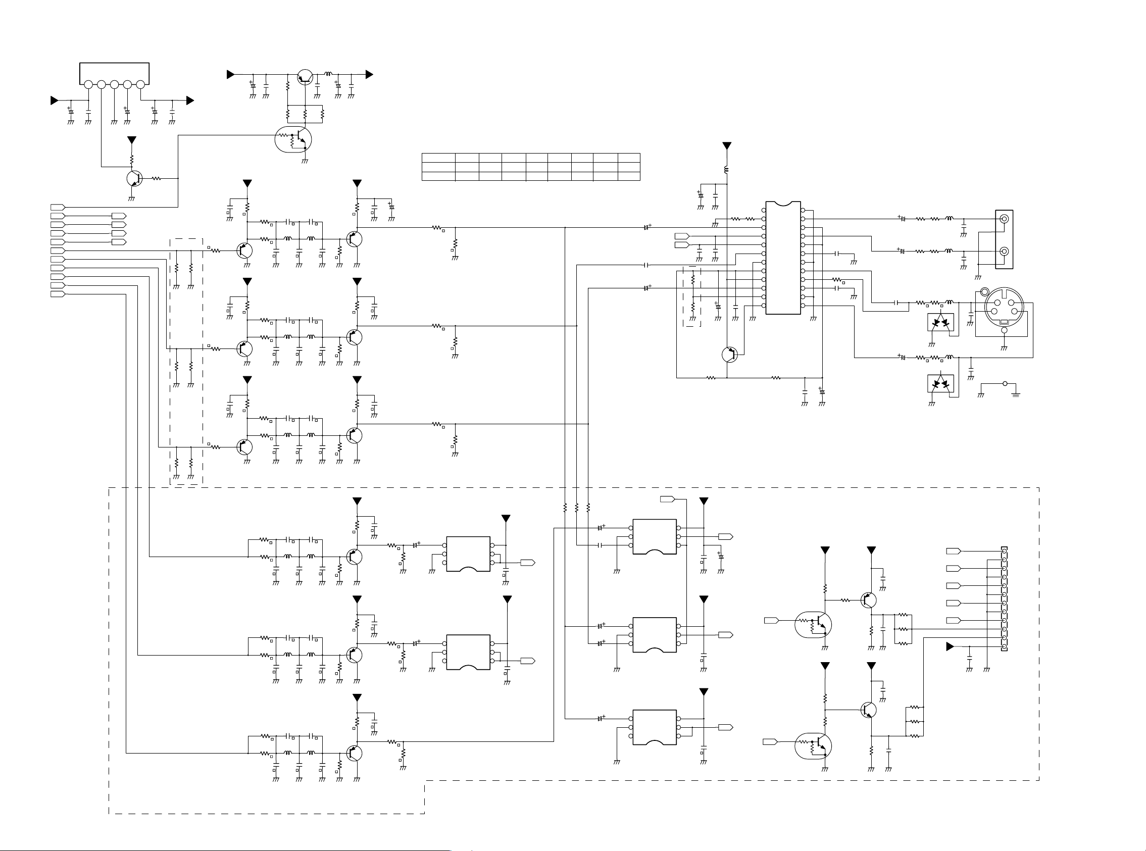
QV01
L88MS05T
12345
E+6V
0.1
470/10V
CV02
CV01
V-GND V-GND
+0V
QV12
2SC4116
V-MUTE
SQUEEZE
LETTER
VSEL1
VSEL2 VSEL2
AD_V
AD_C
AD_Y
AD_G
AD_B
AD_R
V-GND
E+6V
1
3
V-GND
SQUEEZE
LETTER
VSEL1
CV03
1/50V
10k
RV47
2
+0.7V
V-GND V-GNDV-GND
RV48
QV02
2SA1797
LV01
6.8
470/16V
CV06
V-GNDV-GND
RV50
1.2k
RV09
680
RV51
1.2k
RV16
680
RV52
1.2k
RV23
680
R893
NC
R855
470
R894
NC
R895
NC
R873
470
+12.2V
CV07
2
QV03
DTC114EUA
10p
CV11
10p
CV19
10p
CV26
27p
C852
V-GND
27p
C862
V-GND
27p
C871
V-GND
0.1
RV01RV02
CV12
NC
LV02
4.7
CV13
CV20
NC
LV04
4.7
CV21
CV27
NC
LV06
4.7
CV28
C853
3p
L851
12
C854
V-GND
C863
3p
L853R864
12470
C864
V-GND
C872 C874
3p 5p
L855
12
C873
V-GND
33p
33p
33p
68p
68p
68p
10k3.3k
+11.5V
V-GND
LV03
LV05
LV07
L852
L854
L856
1
3
CV14
NC
10
CV22
NC
10
CV29
NC
10
C855
5p
15
C865
5p
15
15
RV03
SW+12V
+5.0V+6.1V
CV04
10k
470/10V
***
CV05
+4.9V
RV05RV12
RV19
+5VV
0.1
+5VV
+5.0V
1.8k
RV08
0.01
CV10
V-GND
QV04
2SA1586
RV07
100
RV14
100
RV21
100
0.01
CV18
V-GND
QV06
2SA1586
+0.5V
0.01
CV25
V-GND
QV08
2SA1586
+0.4V
+5.0V
+5.0V
V-GND
RV15
V-GND
RV22
V-GND
+5VV
1.8k
+5VV
1.8k
RV06
V-GNDV-GND
RV13RV20
V-GNDV-GND
V-GNDV-GND
V-GND
3.3k
47p
CV15
V-GNDV-GNDV-GND
47p
CV23
V-GNDV-GNDV-GND
47p
CV30
V-GNDV-GNDV-GND
56p
C856
V-GND
56p
C866
V-GND
56p
C875
V-GND
CV53
+0.9V
0.1
RV04
RV10
RV17
RV24
+0.9V
R856
+0.9V
R865
R874
3.3k
QV05
2SA1586
22k
QV07
2SA1586
+1.2V
22k
QV09
2SA1586
+1.1V
22k
Q852
2SA1586
22k
V-GND
Q855
2SA1586
22k
V-GND
Q858
2SA1586
22k
+12.2V
CV08
V-GNDV-GND
470/16V
+5VV
2.2k
RV11
V-GNDV-GND
+5VV
2.2k
RV18
V-GNDV-GND
+5VV
2.2k
RV25
V-GNDV-GND
+5VV
2.2k
R857
V-GND
+5VV
2.2k
R866
V-GND
+5VV
2.2k
R875
V-GNDV-GND
CV09
+5.0V
+5.0V
+5.0V
+5.0V
+5.0V
+5.0V
+1.6V
0.1
+1.8V
+1.7V
+1.6V
+1.6V
CV16
CV24
CV31
C857
C867
C876
+12VV
0.01
V-GND
0.01
V-GND
0.01
V-GND
0.01
V-GND
0.01
V-GND
0.01
V-GND
CV17
100/10V
V-GND
R858
0
V-GND V-GND
R867
0
V-GND
R876
0
N.C. N.C.
R877 R868
V-GND
PM01-3/5
***
N ONLY
EXCEPT N
RV41
0
RV43
0
RV45
0
C859
10/50V
4
5
6
N.C
R859
MM1509XN
Q853
C868
10/50V
4
5
6
V-GND
MM1509XN
Q856
RV05 RV06 RV12 RV13 RV19 RV20 RV28 RV29
680
560
470 470 470 470 470 470 0 NC
NC
RV42
V-GND
NCNC
RV44RV46
V-GND
V-GND
0
0
0
+5VV
3
+5.0V
2
SCT_G
1
0.01
C860
V-GND
+5VV
+5.0V
3
2
SCT_B
1
0.01
C869
V-GND
R878
R879
R880
C877
10/50V
C878
0.1
C881
10/50V
C882
10/50V
C884
10/50V
+12VV
NC
V-GND
V-GND
0680 680560 560
4
5
6
MM1506XN
Q859
4
5
6
MM1508XN
Q860
4
5
6
MM1509XN
Q861
CV33
CV32
10/50V
CV34
10/50V
VSEL2
SQUEEZE
0.1
LETTER
CV35
RV29 RV28
V-GND
***
+5.0V
3
2
1
+5.0V
3
2
1
+5.0V
3
2
1
+12.2V
100/16V
V-GND
V-GND
V-GND
47P
CV38
CV37
V-GND V-GND
CV39
100/16V
V-GND
QV10
2SA1162
RV30
0
+5VV
0.01
C879
C880
V-GND
V-GND
+5VV
0.01
C883
V-GND
+5VV
0.01
C885
V-GNDV-GND
LV08
0.1
CV36
47P
3
1
SCT_R/C
10/50V
SCT_V/Y
SCT_V
BLM11B601S
CV40
+12.1V
+8.4V
RV27RV26
3.9K1.2K
0.1
2
+11.4V
SQUEEZE
VSEL1
LA7138M
1
MUTE
2
TYPE_SEL
3
V,Cb_IN
4
SQUEEZE
5
LETTER
6
C,Cr_IN
7
GND
8
REG_OUT
9
VCC
10
Y_IN
11
AMP_SEL
12
DAC_DCOUT
RV31
0
RGB:+3.2V
CVBS/S:+0V
16:9:+3.1V
4:3:+0V
QV11
C_DCOUT
GND
V_OUT
YCMIX
Cb_OUT
VCC
C_OUT
GND
Cr_OUT
Y_OUT2
GND
Y_OUT1
V-GND
CVBS/S:+5.0V
2
Q862
DTC114EUA
2
Q864
DTC114EUA
24
23
22
21
20
CV42
0.1
19
18
17
16
15
14
13
V-GNDV-GNDV-GND
0.1
CV51
RGB:+0V
V-GND
RV32
10K
CV41
0.1
V-GND
470/16V
CV52
V-GND
+5VV
+5.0V+12.2V
R882
22k
R881
1k
2
1
RGB:+5.0V
CVBS/S:+0V
3
V-GND
+12VV
4.7K
R887
16:9:+6.0V
2
4:3:+12.1V
4.7k
R888
16:9:+0V
4:3:+12.1V
1
3
V-GND V-GND
+5VV
V-GND
+12VV
+5.0V
3
1
R883
+12.2V
1
3
16:9:+5.5V
4:3:+11.5V
V-GND
1000/6.3V
1000/6.3V
V-GND
Q863
2SA1586
56k
V-GND
V-GND
Q865
2SC4116
56k
R889
CV43
CV44
CV45
0.1
CV46
1000/6.3V
0.1
C886
R884
220
R885
220
N.C.
C890
R886
220
0.1
C887
0.1
C888
RV33 RV34
RV35
47
DV01
01ZA8.2
V-GND
DV02
01ZA8.2
R890
1.5k
R891
1.5k
R892
1.5k
47 15
RV36
RV37
33
31
RV39
33
31
V-GND
SCT_V/Y
SCT_R/C
15
RV38
27 0
2
2
SCT_V
SCT_G
SCT_B
+12VV
LV09
LV10
LV12RV40
027
0
0
LV11
CV47CV48
N.C.N.C.
V-GND
V-GND
CV49
V-GND
CV50
+12.2V
C889
V-GND
N.C
N.C
V-GND
0.1
V-GND
JV01
1
2
3
4
JV02
6
4
3
2
5
V-GND
JV07
V-GND EARTH
N only
J851
12
V
11
V-GND
10
V/Y
9
V-GND
8
R/C
7
V-GND
6
G
5
V-GND
4
B
3
RGB SW
2
F-SW
1
+12VV
V-GND
1
CVBS
S1/S2
2625
Page 21
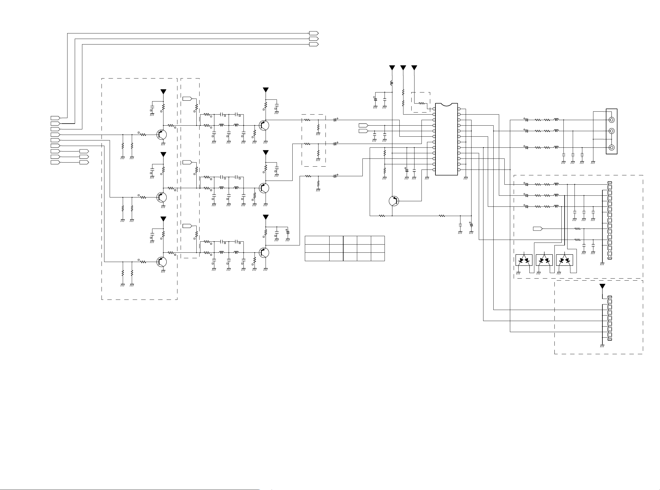
SQUEEZE:+3.1V
SQUEEZE:+0V
Prog:+5.0V Int:+0V
LETTER:+3.1V
LETTER:+0V
SQUEEZE
LETTER
P/XI
SQUEEZE
LETTER
P/XI
PR2_Cr
PR2_Cb
PR2_Y
AD_Cr
AD_Cb
AD_Y
PM01-4/5
N ONLY EXCEPT N
RC03
100
68
N.C.N.C.
RC01
AD_Cr
AD_Cb
AD_Y
RC02RY02
V-GNDV-GND
68
RB01
RB02
V-GNDV-GND
68
RY01
V-GNDV-GND
RB03
100
N.C.
RY03
100
+5.0V
CC01
0.01
V-GND
QC01
2SA1586
+0.5V
+5.0V
0.01
CB01
V-GND
QB01
2SA1586
+0.5V
+5.0V
0.01
CY01
V-GND
QY01
2SA1586
+0.4V
+5VV
1.8k
RC04
V-GND
+5VV
1.8k
RB04
V-GND
+5VV
1.8k
RY04
V-GND
+1.2V+1.2V
+1.0V
RC23
0
RB23
0
RY23
0
AD_Cr
AD_Cb
AD_Y2
RC25RB25RY25
000
CC03
RC24
3p
NC
LC02
LC01
RC05
4.7
390
10p
33p
CC04
V-GND V-GND
CB03 CB05
3p 7p
LB01
LB02
4.7
CB04
10p
33p
V-GND
CY03
3p
LY01
LY02
4.7
33p
10p
CY04
V-GND
V-GND
RB24
NC
RB05
390
RY24
NC
RY05
390
CC02
CB02
CY02
CC05
7p
5.6
5.6
CY05
7p
5.6
CC06
22p
V-GND
CB06
22p
V-GND
22p
CY06
V-GND
+1.3V
RC06
V-GNDV-GND
+1.3V
RB06
V-GND
+1.2V
RY06
V-GND
22k
22k
22k
QC02
2SA1586
QB02
2SA1586
QY02
2SA1586
+5VV
2.2k
RC07
+5VV
RB07
2.2k
V-GNDV-GND
+5VV
2.2k
RY07
V-GND
+5.0V
+2.0V
+5.0V
+2.0V
+5.0V
+1.8V
CC07
CB07
CY07
0.01
V-GND
0.01
V-GND
0.01
V-GND
CY08
V-GND
100/10V
***
RC08
RB08
***
RY08
N
V-GND
V-GND
RY09 RB09 RC09
V-GND
CC08
10/50V
CB08
10/50V
CY09
10/50V
RB08
3.3k
SQUEEZE
LETTER
RB09
RC08
3.3k
0EXCEPT N 0
+12.2V
CY10
100/16V
V-GND
V-GND
47P
CY12
CY13
V-GND V-GND
0
RY14 RY13
V-GND
QY03
2SA1162
RY15
0
RC09
5.6k5.6k
N.C.N.C.
+12VV
LY03
0.1
CY11
47P
N.C.
3
1
+5VV
BLM11B601S
3.9K 1.2K
RY12 RY11
CY14
100/16V
V-GND
2
+8.4V
+5.0V
+11.4V
+5VV
+5.0V
Except F,S,C,L,A
CY15
0.1
RY10
0
1
MUTE
2
TYPE
3
A_IN
4
SQUEEZE
5
LETTER
6
B_IN
7
GND
8
REG
9
VCC1
10
C_IN
11
AMP_SEL
12
DCOUT
QY04
LA7138M
RY16
0
GND
A_OUT2
YCMIX
A_OUT1
VCC2
B_OUT2
GND
B_OUT2
C_DCOUT
C_OUT2
GND
C_OUT1
V-GNDV-GNDV-GND
V-GND
24
23
22
21
20
19
18
17
16
15
14
13
470/16V
0.1
CY17
CY16
V-GND
CY18
1000/6.3V
V-GND V-GND V-GND
RY17 RY18
CB09
RB10
470/6.3V
CC09
RC10
470/6.3V
CY20
RY21
1000/6.3V 27
CB11 LB04
RB12
470/6.3V 0
CC11
RC12
470/6.3V
Prog:+5.0V
Int:+0V
P/XI
2
31
33 27
RB11
27
33
RC11
27
33
RY22
33
RB13
27
33
RC13
27
33
2NC
31
LY04
0
LB03
0
LC03
0
N.C.
CY19
V-GNDV-GND V-GND
LY05
0
LC04
0
DY01DB01DC01
NC
2NC
31
N.C.
N.C.
CB10
CC10
N.C.
N.C.
CY21
CB12
V-GNDV-GND V-GND
10K
RY19
10K
RY20
0.1
CY22
V-GNDV-GND
V-GND
CC12
CY23
JY01
5
3
2
4
1
N.C.
0.1
V-GND
10
11
12
13
14
JY02
1
2
3
4
5
6
7
8
9
Y
Cb
Cr
Y
Y_GND
Cb
Cb_GND
Cr
Cr_GND
N.C.
LINE
I/P
N.C.
ASPECT
SWGND
N.C.
SW
D1/D2
For F,S,C,L,A
+12VV
JY03
8
+12VV
7
V-GND
6
Cb
5
V-GND
4
Cr
3
V-GND
2
Y
1
V-GND
27 28
ONLY OEM
V-GND
Page 22
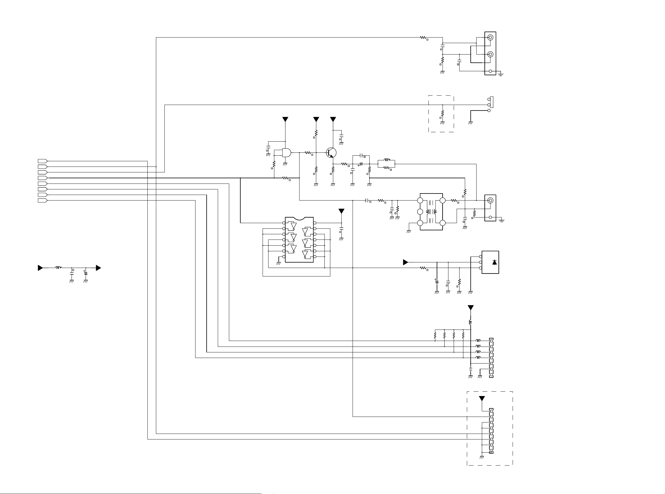
P_TRG
D-BUS
IR_SW
D_OUT
TXD
RXD
DTR
CTS
SW+5V
PM01-5/5
LI01
BLM11B601S
CI10
D-GND
0.01
CI11
100/10V
D-GND
+5.0V
+5VD
N.C.
CI01
D-GND
+5VD +5VD
+5.0V
14
1
2
7
N.C.
RI02
D-GND
RI03
0
QI01
N.C.
1234567
D-GND
+5.0V
1.8k3.9k
RI05RI06
QI02 QI03
N.C.
3
2SC4116
RI04
2.2k
D-GND D-GND
141312111098
JI01
0
RI10
220p
CI12
CI13
22
RI21
1
D-GND
OEM ONLY
+5VD
+5.0V
0.1
CI02
C
D-GND
1
2
B
E
3
220
RI07
+5VD
+5.0V
D-GND
RI08
68
CI15
N.C.
CI03
CI04
N.C.
CI05
1/50V
N.C.
CI16
N.C.
LI03
N.C.
100k
RI09
RI16
0
D-GNDD-GND
RI11
N.C.
N.C.
D-GND
+5VD
RI12
D-GND
N.C.
2
1
+5.0V
RI14
CI17
D-GND
N.C.
RI22
D-GND
LI02
N.C.
220
CI20
D-GND
47/16V
CI21
D-GND
0.01
RI13
N.C.
43
N.C.
CI18
6
D-GND
RI15
D-GND
D-GND
0
RI17
N.C.
D-GND
+5VD
RI35
1
3
2
4
5
1
2
0
3
321
SI01
321
JI03
JI04
GND
VCC
INPUT
REMOTE
CONTROL
INT/EXT
SW
DIGITAL
OUT
GP1F32T
OPT
OUT
RI31
10K
RI32
10K
RI33
10K
RI34
10K
+5.0V
LI35
0.1
CI31
D-GND
BLM11B601S
0
LI31
0
LI32
0
LI33
LI34
0
D-GND
+5VD
D-GND
3029
7
6
5
4
3
2
1
1
2
3
4
5
6
7
8
JI05
TXD
RXD
DTR
CTS
+5VD
D-GND
N.C.
OEM only
JI06
+5VD
XLR
D-GND
D-GND
REMOTE_IN
P_TRG
D-GND
D-GND
Page 23
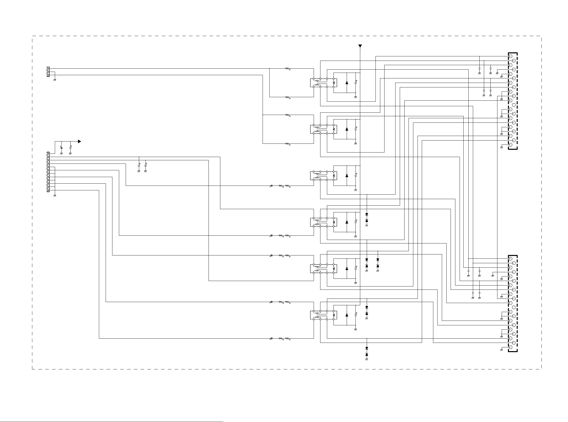
FROM PM01
J950
SAR
3
A-GND
2
SAL
1
A-GND
FROM
PM01
J803
+12VV
12
F-SW
11
RGB SW
10
B
9
V-GND
8
G
7
V-GND
6
R/C
5
V-GND
4
V/Y
3
V-GND
2
V
1
V-GND
PE01
For N
+12.2V
0.01
C802
C801
10/16V
V-GND V-GND
+12VV
0.01
C803
V-GND V-GND
+12VV
R950
100
L950
ED2-12
81035129
R952
100
R951
100
L951
ED2-12
81035129
R953
100
16:9:+5.5V
4:3:+11.5V
Stand by:+0V
RGB:+5.0V
0.01
C804
CVBS/S:+0V
C805
100/10V
R801 R802
39 33
L801
ED2-12
81035129
+12.2V
14
+
+12.2V
14
-
0.010.010.01
C950C951C811
1SS2541SS2541SS2541SS2541SS2541SS254
D950D951D801D802D803D804
A-GND
+
A-GND
+12.2V
14
+
V-GND
330p
C952
A-GND
330p
C954
C953
C955
330p
A-GND
330p
A-GNDA-GND
TV-SCART
1
3
5
A-GND
V-GN D
7
9
11
V-GN D
13
15
V-GN D
17
19
V-GN D
21
V-GN D
J801
2
4
6
8
10
12
14
16
18
20
AR-OUT
AR-IN
AL-OUT
A-GND
V-GND
AL-IN
B-OUT/c-IN
F-SW
V-GND
CONTROL
G-OUT
N.C.
V-GND
V-GND
R/C-OUT
RGB-SW
V-GND
V-GND
CV/Y-OUT
CV/Y-IN
V-GND
C806
100/10V
C807
100/10V
C808
470/6.3V
C809
470/6.3V
R803 R804
39 33
R807 R808
39 33
R809 R810
39 33
L802
ED2-12
81035129
+12.2V
14
+
V-GND
0.01
C812
8.2V 8.2V
D806 D805D807D808D811D812
V-GND
AUX-SCART
R806R805
3339
L803
ED2-12
L804
ED2-12
81035129
81035129
+12.2V
14
+
V-GND
+12.2V
14
+
V-GND
8.2V8.2V8.2V8.2V
0.01
C813
V-GND
0.01
C814
V-GND
V-GND
D810 D809
8.2V 8.2V
V-GN D
D813D814
8.2V8.2V
330p
330p330p
C956
C957C959
A-GND
A-GND
A-GND
330p
C958
A-GND
A-GND
V-GN D
V-GN D
V-GN D
V-GN D
V-GN D
J802
1
AR-OUT
2
AR-IN
3
AL-OUT
4
A-GND
5
V-GND
6
AL-IN
7
B-IN/C-OUT
8
F-SW
9
V-GND
10
CONTROL
11
12
G-IN
N.C.
13
V-GND
14
V-GND
15
R/C-IN
16
RGB-SW
17
V-GND
18
V-GND
19
CV/Y-OUT
20
CV/Y-IN
21
v-GND
31 32
Page 24
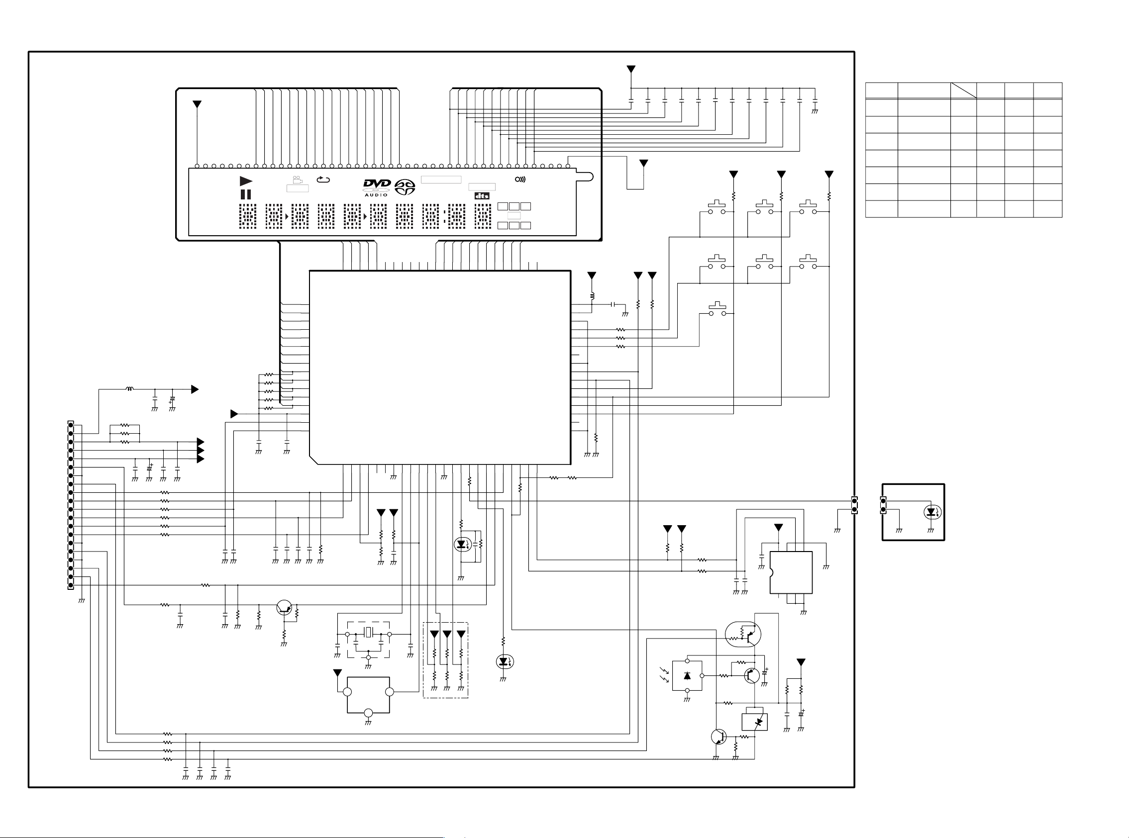
FROM
PM01
D-GND
-27V
DC+3.5V
Heater
E+5V
STB CONT
D-GND
P_TRG
XRESET
S(MtoF)
S(FtoM)
SSCK
XREADY
D-GND
/TEST
D-GND
IR_SW
D-BUS
V_MUTE
JF01
LT1
PF01
1
2
3
4
5
6
7
8
9
10
11
12
13
14
15
16
17
18
19
20
GND
LF01
BLM11B601S
RF49
RF50
RF51
0
NC
NC
CF39
0.01
CF01
0.047
CF40
GND
N.C.
CF41
47/10V
GNDGND GNDGND
RF01
RF02
RF03
RF04
RF05
RF06
RF53
RF54
RF55
RF56
RF57
DC+3.5V
-29.0V
CF02
N.C.
GND
-15.4V
-19.0V
+5.2V
N.C.
CF42
22
22
22
22
22
22
RF07
0
100p
CF34
GND
N.C.
22
22
22
N.C.
100p
CF35
CF36
GND GND GND GND
-15.4V
-27V
DC+3.5V
Heater
+5V
CF37
22
100p
-27V
CF20
CF07
100p
100p
GND
CF38
100p
GND
-29.0V
CF21
100p
RF21
RF44
82K
RF45
82K
RF46
82K
RF47
82K
47k
P17
P18
V-PART
GRP
TITLE
RF43
82K
CF18
0.047
GND
+3.4V
RF10
GND
10K
P16
RF08
4.7K
P15
P13
P12
P11
P10
P9
P8
P7
P6
P5
P4
P3
P2
P1
GND
100p
CF03
GNDGNDGND
QF02
2SA1586
GND
P14
P13
V OFF
QF01
TMP87PM74F
65
66
67
68
69
70
71
72
73
74
75
76
77
78
79
80
CF19
0.047
100p
CF04
GND
+3.4V
+2.7V
RF09
P12
100p
CF05
GNDGND
4.7K
P8
P6
P7
P16
P15
SOUT(FtoM)
RESET OUT
XF01
3
GND
P4
P2
P3P5P1
P18
P17
XRDY
GND GND
+5V
+5V
+5.2V
N.C.47K
RF24RF25
RF11
CF08
GND
GND
CSTS8.0MHZ(MG)
3
QF04
GND
PST600D-2
INOUT
2
1
GND
+5.2V
47K
0.047
GND
+5.1V
XOUT
CF10
N.C.
GNDGND
PROGRESSIVE
LAST
TOTAL
RESET
XIN
+5V +5V
+5.2V
RF13
RF14
GND
COND
REMAIN
G2
G1
RF15
RF16
(*1)
G11
TEST
DF04
ILM_LED
+5.2V
G10
G4
G3
GND
+5V
+5.2V
RF18 RF17
GNDGND
G9G8G7
SURROUND
DOLBY D
G6
G5
STB LED
FL_OFF
1k
RF19
NC
CF43
270
RF48
P9
P10
P11
192kHz
VCD
96kHz
TRKD OFF
CHP
P14
64 63 62 61 60 59 58 57 56 55 54 53 52 51 50 49 48 47 46 45 44 43 42 41
VKK
SCK
SIN(MtoF)
1 23456789101112131415161718192021222324
100p
NC
RF12
CF06
GND
12
N.C.
CF09
+5V
+5.2V
G6
G8
G7
STB_CONT
NC
RF61
G5G3G4G1G2
5.1CH
DOWN MIX
C
L
LFE
S
LS
G9
G10
G11
D BUS IN
LT1
V_MUTE
RF60
1k
RF20
DF03
FL_OFF
GND
R
RS
INT4/TC3
0
EEP_SCL
EEP_SDA
123456789101112131415161718192021222324252627282930313233343536373839404142434445
P_TRG
RF58 RF59
NC
NC
-27V
-29.0V
CF29
CF28
100p
100p
100p
SF07
RF28
22K
+5.1V
RF31
2.2K
CF14
RF30
CF30
100p
+5V +5V +5V
+5.2V
RF40 RF41 RF42
4.7K 4.7K 4.7K
STOP
PREVIOUS/REW
GND GND
N.C.
N.C.
CF15
GNDGND
QF05
DTA114EU
+5.1V
RF29
N.C.
+5.3V
QF07
GND
2SA1586
10K
31
+0V
2
RF32
10K
+5.2V
3
2
GND
RF23
CF26
10k
ZF01
100p
RF26
100
RF27
100
QF06
2SC4116
1
CF27
SF01
PAUSE
/STILL
SF04 SF05
NEXT/FF
FL.OFF
GND GND
100p
CF22
VF01
+5V
LF03
+5.2V
BLM11B601S
CF17
GND
GND
RF35
0.1
RF36
RF37
RF38
47k
GND
100
100
100
40
39
38
37
36
35
34
33
32
31
30
29
28
27
26
25
-19.0V
+5V
+5.2V
CF23
Heater
100p
4.7K
RF52
+5V
+5.2V
CF24
4.7K
RF39
100p
+5V
+5.2V
RF22
10k
CF25
100p
+5V
CF31
100p
+5.2V
+5V
+5.2V
8765
0.1
CF16
1234
CF11
10/16v
DF01
1SS301
GND
CF32
100p
SF03SF02
PLAY
SF06
OPEN/CLOSE
GND
+5V
100
RF33
0.1
CF12
GND
0.047
CF33
GND
+5.2V
100
RF34
+5.1V
CF13
100/6.3V
(EJ)
+5.2V
QF08
AT24C04
(*1)
QF01 Pin No.11,12,14 SETTING
DistinationRegion
2
1
4
3
2
5
6
JF02
JF03
PF02
1
1
2
2
DF02
STAND
BY
GNDGND
JAP AN
USA
AUS
ASIA
EURO
--
CHINA
GND
Pin No.
MS1
0
2L
4
4H
2
11
12
14
L
L
H
L
H
L
H
H
L
L
L1
H
H2
L
H
L
L
H
H
3433
Page 25
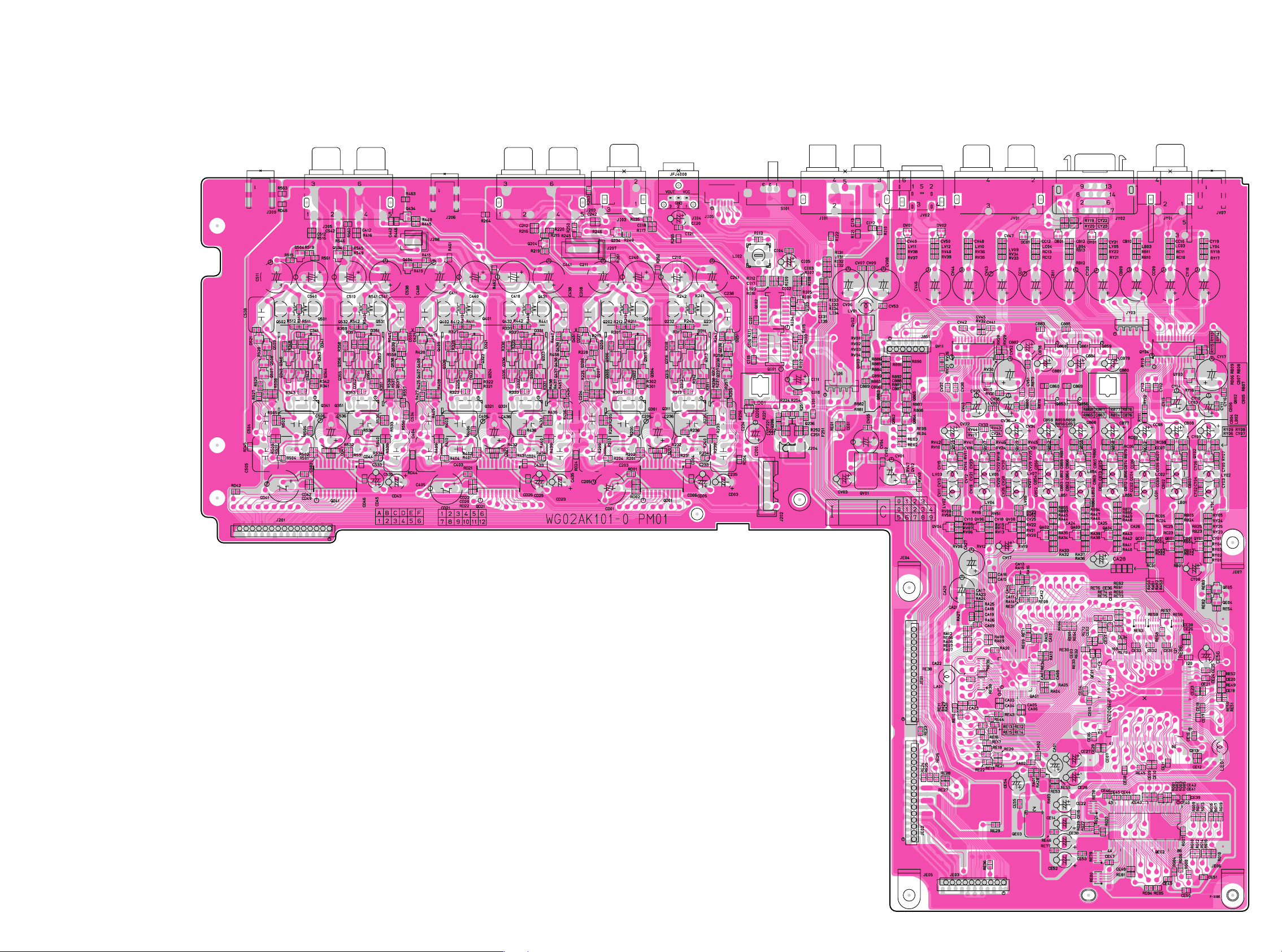
11. PARTS LOCATION
PM01
Q509
Q508
Q507
Q504 Q534
Q502 Q501
Q346 Q343
Q345 Q344
Q532 Q531
Q356 Q353
Q355 Q354
QD41
Q434
Q404
Q539 Q409
Q538 Q408
Q537 Q407
Q402 Q401
Q326 Q323
Q325 Q324
Q432 Q431
Q336 Q333
Q335 Q334
QD21
Q204
Q439 Q209
Q438 Q208
Q437 Q207
Q234
Q202 Q201
Q306 Q303
Q305 Q304
Q232 Q231
Q316 Q313
Q315 Q314
QD01
Q239
Q238
Q237
QI02
QI01
Q206 Q236
QV02
QV01
Q863 Q865
Q862 Q864
QV12
QV11
QV10
QV05 QV07 QV09 Q852 Q855 Q858 QC02 QB02 QY02
QV04 QV06 QV08 QA02 QA03 QA04 QC11 QB01 QY01
QA01
Q860 Q861 Q859
Q853 Q856
QE03
QE01
QE02
QY04
QY03
QE05 QE04
35 36
Page 26
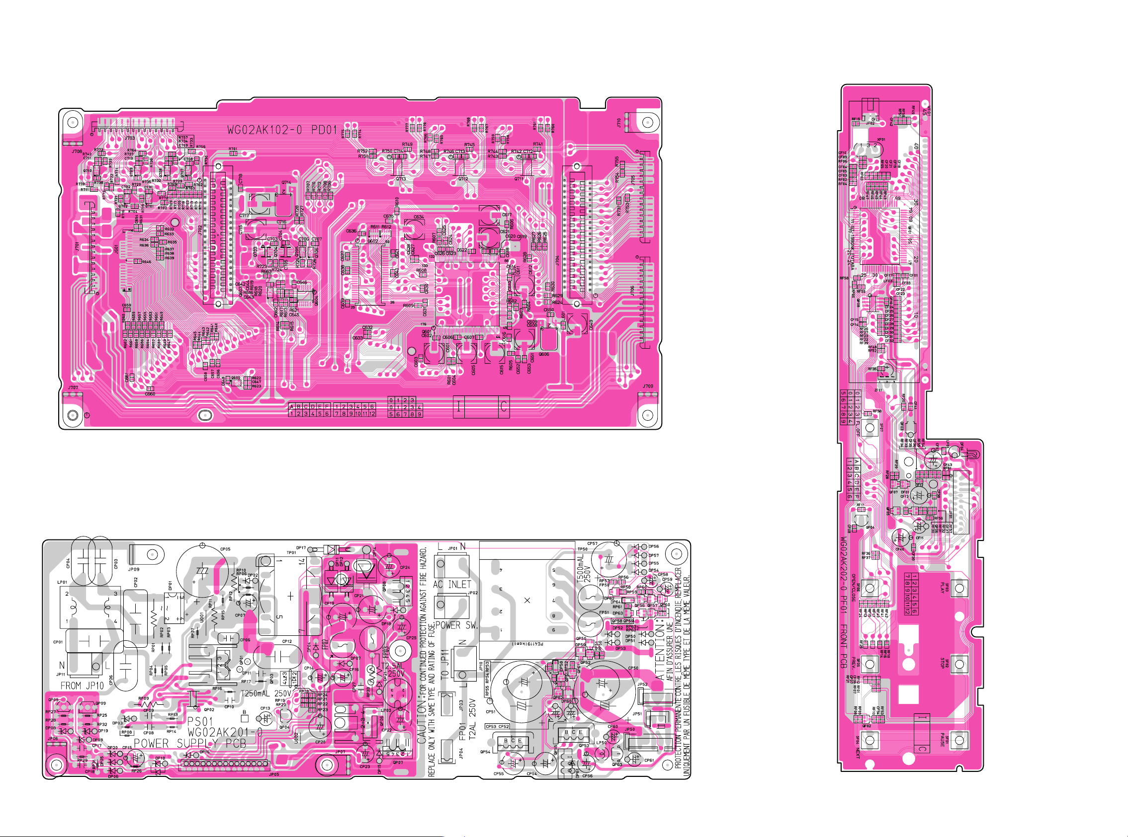
PD01
Q710 Q709 Q708 Q707
Q702 Q701
Q703 - Q706
Q603 Q604 Q602
Q713
Q712
Q601
Q711
PF01
QF01
PS01
QP05 QP09
QP02
QP01
QP04
QP08
QP06 QP07
QP51 QP61 QP62
QP54
QP50 QP52
QP53 QP63
QP56 - QP60
QF07
QF05 QF06
QF04
QF02
3837
Page 27
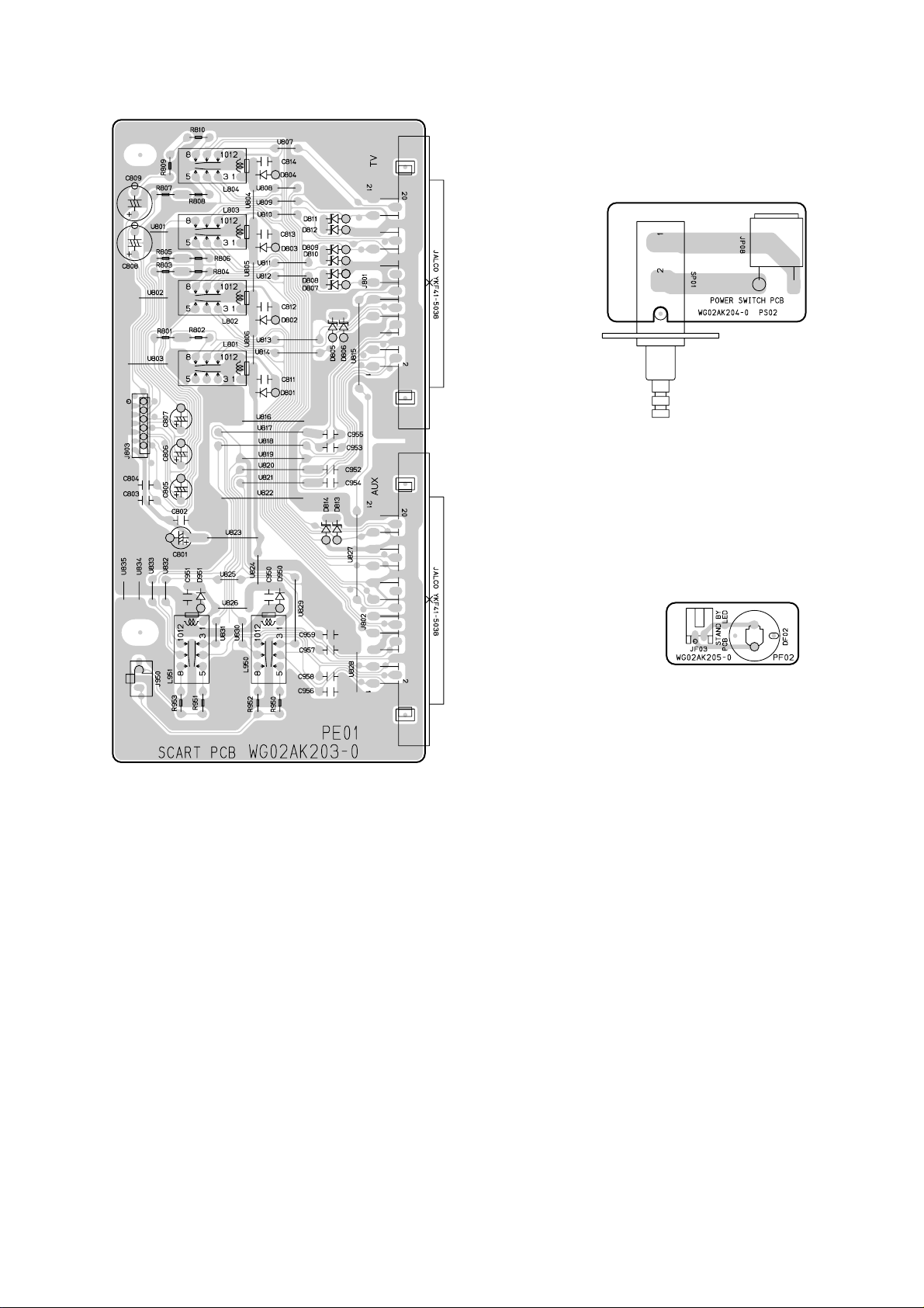
PE01 [N ONLY]
PS02
PF02
39
Page 28

12 MICROPROCESSOR AND IC DATA
QF01:TMP87CM71F
Pin PORT Signal name I/O Contents of control
1 P02/SO1 SOUT (F to M) O Serial bus data output for DV747
2 P03 RESET_OUT O For the DV747 RESET terminal control RESET: L
3 P04 DV8300/DV8310 I Setup of Model Circuit diagram reference
4 P05 XRDY O Serial data communication request signal for DV747 High: request /Low: no
5 P06 N C
6 P07 N C
7 VSS GND
8 XOUT 8MHz X'TAL
9 XIN 8MHz X'TAL
10 RESET RESET I Reset signal for the microcomputer
11 P22 MODEL1 I Set up of version Circuit diagram reference
12 P21 MODEL2 I Set up of version Circuit diagram reference
13 TEST GND
14 P20 MODEL3 I Set up of version Circuit diagram reference
15 P10 ILM_LED O ILM LED for FL Light burned: H
16 P11 STB_LED O It is light at the STANDBY Light burned: H
17 P12 FL_OFF_LED O Lighting (FL Lights-out) Light burned: H
18 P13 STB_CONT O Power supply control for DV747 Stand-by time: LOW
19 P14 V_MUTE O Mute control for Video At the time of Mute: L
20 P15 LT1 I Serial bus data Ready/Busy input for DVD747 High: Ready/Low: Busy
21 P16 D_BUS_IN I D-BUS input
22 P17/TC3 IR I IR sensor input
23 P30 SCL O I2C clock (EEPROM control) AT24C04
24 P31 SDA I/O I2C data (EEPROM control) AT24C04
25 P32 GND
26 P40 N C FL Lights-out
27 P41 KEY_IN_0 I Key matrix input (Tactile switch)
28 P42 KEY_IN_1 I Key matrix input (Tactile switch)
29 P43 KEY_IN_2 I Key matrix input (Tactile switch)
30 P44 KEY_IN_3 I Key matrix input (Tactile switch) spare
31 P45 PowerTrigger I By the AD change, Power decision Setup of Model is Linkage with
32 P46 SreviceKey I Service function switching
33 P47 GND
34 P50 KEY_OUT_0 O Tactile switch spare
35 P51 KEY_OUT_1 O Tactile switch
36 P52 KEY_OUT_2 O Tactile switch
37 P53 KEY_OUT_3 O Tactile switch
38 VASS GND GND for A/D
39 VAREF 5V O A reference voltage for A/D
40 VDD 5V Power supply
40
Page 29

Pin PORT Signal name I/O Contents of control
41 P60 NC
42 P61 NC
43 P62 G11 O FL indication
44 P63 G10 O FL indication
45 P64 G9 O FL indication
46 P65 G8 O FL indication
47 P66 G7 O FL indication
48 P67 G6 O FL indication
49 P70 G5 O FL indication
50 P71 G4 O FL indication
51 P72 G3 O FL indication
52 P73 G2 O FL indication
53 P74 G1 O FL indication
54 P75 N C
55 P76 N C
56 P77 N C
57 P80 N C
58 P81 N C
59 P82 N C
60 P83 P18 O FL indication
61 P84 P17 O FL indication
62 P85 P16 O FL indication
63 P86 P15 O FL indication
64 P87 P14 O FL indication
65 P90 P13 O FL indication
66 P91 P12 O FL indication
67 P92 P11 O FL indication
68 P93 P10 O FL indication
69 P94 P9 O FL indication
70 P95 P8 O FL indication
71 P96 P7 O FL indication
72 P97 P6 O FL indication
73 PD00 P5 O FL indication
74 PD01 P4 O FL indication
75 PD02 P3 O FL indication
76 PD03 P2 O FL indication
77 PD04 P1 O FL indication
78 VKK -27V Power supply for the FL drive
79 P00/SCK1 SCK O Serial bus clock output for DV747
80 P01/SI1 SIN (M to F) I Serial bus data input for DV747
41
Page 30
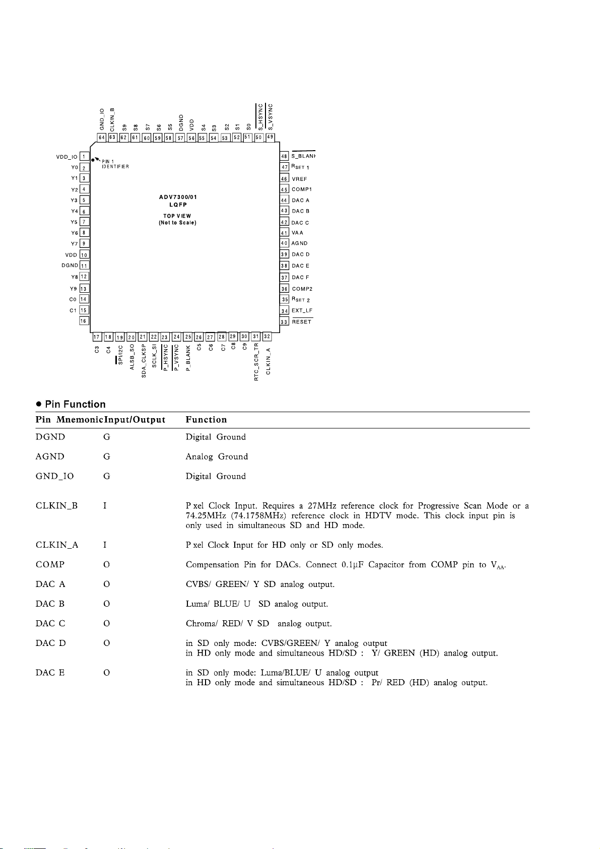
QA01 : ADV7300KST
• Video Encoder IC
Pin Arrangement
•
42
Page 31

43
Page 32

QE01 : PM0033A
• Progressive Scan Converter (PRO2)
Pin Arrangement
•
44
Page 33

•
Pin
Function
Pin
No.
1 VDD3 P 2CLKIInLVTTL
3 PLL_TEST In LVTTL
4 PLL_EN In LVTTL
5 VDD2 P 6CLKOOut2mA
7 PD0 Inout LVTTL, leakage, 2mA
8 PD1 Inout LVTTL, leakage, 2mA
9 PD2 Inout LVTTL, leakage, 2mA
10 PD3 Inout LVTTL, leakage, 2mA
11 PD4 Inout LVTTL, leakage, 2mA
12 GND P 13 VDD3 P 14 PD5 Inout LVTTL, leakage, 2mA
15 PD6 Inout LVTTL, leakage, 2mA
16 PD7 Inout LVTTL, leakage, 2mA
17 PD8 Inout LVTTL, leakage, 2mA
18 PD9 Inout LVTTL, leakage, 2mA
19 GND P 20 GND P 21 GND P 22 VDD3 P 23 NHS In Schmitt
24 NVS In Schmitt
25 PA0 In
26 PA1 In
27 PA2 In
28 PA3 In
29 PA4 In
30 PA5 In
31 PA6 In
32 PA7 In
33 PA8 In
34 PA9 In
35 MA4 Out 2mA
36 MA3 Out 2mA
37 MA5 Out 2mA
38 MA2 Out 2mA
39 GND P 40 VDD3 P -
Name
I/O/
Attribute Functional Description
P
LVTTL
LVTTL
LVTTL
LVTTL
LVTTL
LVTTL
LVTTL
LVTTL
LVTTL
LVTTL
VDD for IO (3.3V)
27MHz System clock input terminal
Test exclusive use input terminal
PLL enable input terminal
VDD for Core (2.5V)
27MHz Clock output terminal
Image data I/O port D(LSB)
Image data I/O port
Image data I/O port
Image data I/O port
Image data I/O port
Digital Ground
VDD for IO (3.3V)
Image data I/O port
Image data I/O port
Image data I/O port
Image data I/O port
Image data I/O port D(MSB)
Digital Ground
Digital Ground
Digital Ground
VDD for IO (3.3V)
Horizontal synchronization input terminal
Vertical synchronization input terminal
Image data I/O port A(LSB)
Image data I/O port
Image data I/O port
Image data I/O port
Image data I/O port
Image data I/O port
Image data I/O port
Image data I/O port
Image data I/O port
Image data I/O port A(MSB)
SDRAM address output terminal
SDRAM address output terminal
SDRAM address output terminal
SDRAM address output terminal
Digital Ground
VDD for IO (3.3V)
D
D
D
D
D
D
D
D
A
A
A
A
A
A
A
A
45
Page 34

Pin
No.
Name
I/O/
Attribute Functional Description
P
41 VDD2 P 42 MA6 Out 2mA
43 MA1 Out 2mA
44 MA7 Out 2mA
45 MA0 Out 2mA
46 MA8 Out 2mA
47 MA10 Out 2mA
48 VDD3 P 49 MA9 Out 2mA
50 MA11 Out 2mA
51 GND P 52 RAS Out 2mA
53 MCLK Out 4mA
54 CAS Out 2mA
55 WE Out 2mA
56 VDD3 P 57 MD8 Inout LVTTL, 2mA, Pullup
58 MD7 Inout LVTTL, 2mA, Pullup
59 MD9 Inout LVTTL, 2mA, Pullup
60 PDOEN In LVTTL
61 GND P 62 GND P 63 MD6 Inout LVTTL, 2mA, Pullup
64 MD10 Inout LVTTL, 2mA, Pullup
65 VDD3 P 66 MD5 Inout LVTTL, 2mA, Pullup
67 MD11 Inout LVTTL, 2mA, Pullup
68 MD4 Inout LVTTL, 2mA, Pullup
69 MD12 Inout LVTTL, 2mA, Pullup
70 MD3 Inout LVTTL, 2mA, Pullup
71 MD13 Inout LVTTL, 2mA, Pullup
72 GND P 73 VDD3 P 74 MD2 Inout LVTTL, 2mA, Pullup
75 MD14 Inout LVTTL, 2mA, Pullup
76 MD1 Inout LVTTL, 2mA, Pullup
77 MD15 Inout LVTTL, 2mA, Pullup
78 MD0 Inout LVTTL, 2mA, Pullup
79 VDD2 P 80 VDD3 P 81 VDD3 P 82 GND P 83 MD16 Inout LVTTL, 2mA, Pullup
VDD for Core (2.5V)
SDRAM address output terminal
SDRAM address output terminal
SDRAM address output terminal
SDRAM address output terminal(LSB)
SDRAM address output terminal
SDRAM address output terminal
VDD for IO (3.3V)
SDRAM address output terminal
SDRAM address output terminal(MSB)
Digital Ground
SDRAM Row Address StrobeCommand output terminal
SDRAM Clock output terminal (54MHz)
SDRAM Column Address Strobe
Command output terminal
SDRAM Write Enableoutput terminal
VDD for IO (3.3V)
SDRAM data input-output terminal
SDRAM data input-output terminal
SDRAM data input-output terminal
Image port D input and output setting input terminal
(L: input, H: output )
Digital Ground
Digital Ground
SDRAM data input-output terminal
SDRAM data input-output terminal
VDD for IO (3.3V)
SDRAM data input-output terminal
SDRAM data input-output terminal
SDRAM data input-output terminal
SDRAM data input-output terminal
SDRAM data input-output terminal
SDRAM data input-output terminal
Digital Ground
VDD for IO (3.3V)
SDRAM data input-output terminal
SDRAM data input-output terminal
SDRAM data input-output terminal
SDRAM data input-output terminal
SDRAM data input-output terminal(LSB)
VDD for Core (2.5V)
VDD for IO (3.3V)
VDD for IO (3.3V)
Digital Ground
SDRAM data input-output terminal
46
Page 35

Pin
No.
84 MD17 Inout LVTTL, 2mA, Pullup
85 MD18 Inout LVTTL, 2mA, Pullup
86 MD19 Inout LVTTL, 2mA, Pullup
87 GND P 88 AGND P 89 DAO_Y Out 90 AVDD2 P 91 DAO_Cb Out 92 AGND P 93 DAO_Cr Out 94 AVDD2 P 95 VREF In 96 FSADJ Inout 97 AVDD2 P 98 VG Out -
99 AGND P 100 GND P 101 GND P 102 GND P 103 GND P 104 CLMP Out 2mA
105 TEST0 In LVTTL
106 TEST1 In LVTTL
107 TEST2 In LVTTL
108 TEST3 In LVTTL
109 TEST4 In LVTTL
110 SPR0 Out 2mA
111 SPR1 Out 2mA
112 VDD3 P 113 SPR2 Out 2mA
114 SPR3 Out 2mA
115 SPR4 Out 2mA
116 SPR5 Out 2mA
117 GND P 118 SPR6 Out 2mA
119 SPR7 Out 2mA
120 VDD3 P 121 VDD2 P 122 GND P 123 PB0 Inout LVTTL, leakage, 2mA
124 PB1 Inout LVTTL, leakage, 2mA
125 PB2 Inout LVTTL, leakage, 2mA
126 PB3 Inout LVTTL, leakage, 2mA
127 VDD3 P 128 PB4 Inout LVTTL, leakage, 2mA
Name
I/O/
Attribute Functional Description
P
SDRAM data input-output terminal
SDRAM data input-output terminal
SDRAM data input-output terminal(MSB)
Digital Ground
Ground for DAC
Analog video-out (Y)
VDD for DAC (2.5V)
Analog video-out (Cb)
Ground for DAC
Analog video-out (Cr)
VDD for DAC (2.5V)
DAC reference voltageinput terminal
An ohms connection terminal for DAC peak swing setting
VDD for DAC (2.5V)
A volume connection terminalfor gate voltage
compensation of a DACelectric current cell
Ground for DAC
Digital Ground
Digital Ground
Digital Ground
Digital Ground
Clamp pulse output terminal
Test exclusive use input terminal
Test exclusive use input terminal
Test exclusive use input terminal
Test exclusive use input terminal
Test exclusive use input terminal
Serial-to-parallel conversion output terminal(LSB)
Serial-to-parallel conversion output terminal
VDD for IO (3.3V)
Serial-to-parallel conversion output terminal
Serial-to-parallel conversion output terminal
Serial-to-parallel conversion output terminal
Serial-to-parallel conversion output terminal
Digital Ground
Serial-to-parallel conversion output terminal
Serial-to-parallel conversion output terminal(MSB)
VDD for IO (3.3V)
VDD for Core (2.5V)
Digital Ground
Image data I/O port B(LSB)
Image data I/O port B
Image data I/O port B
Image data I/O port B
VDD for IO (3.3V)
Image data I/O port B
47
Page 36

Pin
No.
Name
I/O/
Attribute Functional Description
P
129 PB5 Inout LVTTL, leakage, 2mA
130 GND P 131 PB6 Inout LVTTL, leakage, 2mA
132 PB7 Inout LVTTL, leakage, 2mA
133 PB8 Inout LVTTL, leakage, 2mA
134 PB9 Inout LVTTL, leakage, 2mA
135 PBOEN In LVTTL
136 VDD3 P 137 PC0 Out 2mA
138 PC1 Out 2mA
139 PC2 Out 2mA
140 PC3 Out 2mA
141 GND P 142 GND P 143 PC4 Out 2mA
144 PC5 Out 2mA
145 VDD3 P 146 PC6 Out 2mA
147 PC7 Out 2mA
148 PC8 Out 2mA
149 PC9 Out 2mA
150 GND P 151 CSB In Schmitt
152 SDA In Schmitt
153 SCL In Schmitt
154 SRN In Schmitt
155 CKIPOL In LVTTL
156 PLL_VDD P 157 CPOUT Out Analog
158 VCOIN In Analog
159 PLL_GND P 160 VDD3 P -
Image data I/O port
B
Digital Ground
Image data I/O port
Image data I/O port
Image data I/O port
Image data I/O port
B
B
B
B(MSB)
Image port B input and output setting input terminal
(L: input, H: output )
VDD for IO (3.3V)
Image data I/O port
Image data I/O port
Image data I/O port
Image data I/O port
C(LSB)
C
C
C
Digital Ground
Digital Ground
Image data I/O port
Image data I/O port
C
C
VDD for IO (3.3V)
Image data I/O port
Image data I/O port
Image data I/O port
Image data I/O port
C
C
C
C(MSB)
Digital Ground
MPU Interface chip select input terminal
MPU Interface data entry terminal
MPU Interface clock input terminal
System reset input terminal
System clock polarity setting input terminal
VDD of PLL exclusive use
(2.5V)
Analog output terminal from PLL chargepump
Analog input terminal from PLL outsidecharge
account loop filter
Ground of PLL exclusive use
VDD for IO (3.3V)
48
Page 37

Q601 : CXD2753R
49
Page 38

505152
Page 39

Page 40

Page 41

QY04/QV11:LA7138M
NVUF.TX
TJHOBM.JO/TX
DPNQPTJUF/JO
TRVFF[F/TX
MFUUFS.CPY/TX
D.JO
HOE2
SFH
WDD2
Z/JO
2
3
4
5
6
7
8
9
:
21
QFEFTUBM
DMBNQ
DMBNQ
QFEFTUBM
DMBNQ
DMBNQ
9W
SFH
UP!QFEFTUBM
DMBNQ
5/36W
WSFG
DMBNQ
TZOD
TFQ
Z!D
NJY
3TUFQ
BNQ
3TUFQ
BNQ
D`PGGTFU
ED`DUM
861IN
ESJWFS
861IN
ESJWFS
861IN
ESJWFS
861IN
ESJWFS
861IN
ESJWFS
35 HOE3B
34
DPNQPTJUF/PVU3
33
DPNQPTJUF.T/TX
32
DPNQPTJUF/PVU2
WDD3
31
2:
D/PVU3
29
HOE3C
28
D/PVU2
D.ED/PVU
27
26
Z/PVU3
BNQ/TX
QOQ.C.JO
22
23
3TUFQ
BNQ
861IN
ESJWFS
25
24
HOE3D
Z/PVU2
53
Page 42

54
Page 43

Q859 : MM1506XNRE
Q860 : MM1508XNRE
Q853/Q856/Q861 : MM1509XNRE
55 56
Page 44

13. EXPLODED VIEW AND PARTS LIST
003B
SYMBOL STYL E
5110
5125
5126
5127
5128
5129
5192
MARK MATERIAL/ FINISH
(M) STEEL / COPPER
(U ) STEEL/ BL ACK
001Z
001B
5128
3X10(M)
x2
015Bx3
010Bx2
PARTS NAME
+B.H.M.SCREW
+B. H. TAP T IT E SCREW(P TYPE)
+B.H.TAP TITE SCREWW/WASHER
+P. H. TA P TI T E SCREW(B TYPE)
+B. H. TA P TI T E SCREW(B T YPE)
+B. H. TAP T ITE SCREW(W/T. L . WASHER)
W(
+P.H.M.SCRE
MINUTE)
PS0 2
5126
3X8(M)
045B
008B
x2
PF0 2
VF0 1
5126
3X8(M)
050B
051B
055B
005B
x2
002M
1. 7x9(U)
PD01
057B
056B
5128
3x18(M)
5192
x2
x2
001D
001A
PF0 1
5125
3X8(U)
x4
5128
3x8(M)
x4
5128
3x8(M)
x3
5129
3X8(M)
5128
3x20(U)
x2
003M
5125
3X8(U)
x4
x1
5126
3X8(M)
004M
5125
3X8(U)
x2
x2
5129
3X8(M)
x1
PS0 1
5126
3X8(M)
5128
3X8(M)
L001
(DVDM)
002A
100G
x1
x3
038G x 2
5128
3X5(M)
L011
L002
0 31G x 3
x3
L001
5128
3X8(M)
x4
5110
3X6(M)
x1
L002
PE0 1
901G
5110
3X6(M)
x2
J001
032G
5128
3X5(M)
x2
031G
N VERSION
090G
PM0 1
5110
3X8(M)
5127
3x8(M)
x4
901G
5129
3x8(M)
5127
3x8(M)
x1
NONLY
070Gx2
x4
x3
W001
5127
3x8 (M)
001G
x7
5127
3x8(M)
x2
009B
012B
013Bx2
011B
007B
002B
006B
009G
5126
3X10(M)
x4
I
N
V
A
I
V
S
O
I
I
B
D
L
E
D
I
R
L
E
A
C
S
T
E
R
E
X
R
P
A
O
D
S
U
I
R
A
E
T
I
T
O
O
N
B
E
W
A
H
M
E
.
N
O
P
E
N
.
990G
UONLY
5128
3X8(M)
009G
x4
5128
3X8(M)
x2
005G
010Gx2
5857
012Gx2
UONLY
991G
991G
Page 45

POS.
NO
VERS.
COLOR
PART NO.
(FOR EUR)
DESCRIPTION
PART NO.
(MJI)
POS.
NO
VERS.
COLOR
PART NO.
(FOR EUR)
DESCRIPTION
PART NO.
(MJI)
001A 02AK304500 MECHANISM
02AK304500
DVD LOADER DB-VLD302
002A ZK02AK0210 UNIT KIT DB-VPB305 ZK02AK0210
001B GOLD 02AK105120 FRONT CHASSIS PL L 02AK105120
001B BLACK 02AK105020 FRONT CHASSIS PL L 02AK105020
002B GOLD 02AK105130 FRONT CHASSIS PL R 02AK105130
002B BLACK 02AK105030 FRONT CHASSIS PL R 02AK105030
003B GOLD 02AK248110 FRONT PANEL AL 02AK248110
003B BLACK 02AK248010 FRONT PANEL AL 02AK248010
005B GOLD 02AK270110 BUTTON FUNCTION 02AK270110
005B BLACK 02AK270010 BUTTON FUNCTION 02AK270010
006B GOLD 02AK270120 BUTTON SUB FUNC 02AK270120
006B BLACK 02AK270020 BUTTON SUB FUNC 02AK270020
007B 02AK158010 WINDOW 02AK158010
008B 02AK270030 BUTTON FL OFF 02AK270030
009B
nsp BADGE MARANTZ BL 185J251010
010B 230K355030 LENS STANDBY/FL OFF 230K355030
011B 02AK355010 LENS TRAY UPPER 02AK355010
012B /C/F/L
02AK251010 BADGE SACD GOLD 02AK251010
/N
012B /U BADGE SACD 02AK251020
045B GOLD 02AK270140 BUTTON POWER GOLD 02AK270140
045B BLACK 02AK270040 BUTTON POWER BLACK 02AK270040
050B GOLD 02AK063110 ESCUTCHEON TRAY FRONT 02AK063110
050B BLACK 02AK063010 ESCUTCHEON TRAY FRONT 02AK063010
051B 392K063160 ESCUTCHEON SACD 392K063160
009G 383K057010 LEG PORON GOLD
383K057010
HOT STAMP F
010G 383K057110 LEG PORON GOLD
383K057110
HOT STAMP R
02AK362010 ADAPTOR MECHA L 02AK362010
002M 02AK362020 ADAPTOR MECHA R 02AK362020
003M 02AK271110 HOLDER MECHA 02AK271110
004M
J001 YJ04002550 JACK AC INLET TYPE HF-301 YJ04002550
L007 FC50160030 FERRITE CORE TFCK-16-8-13 FC50160030
L008 FC50230010 FERRITE CORE FC50230010
L009 FC90400010 FERRITE CORE SSC-40-12 FC90400010
L010 FC50160030 FERRITE CORE TFCK-16-8-13 FC50160030
WD01 JUMPER LEAD
nsp
YU40042510
PD01-DIGITAL BOARD
WD02 JUMPER LEAD PD01-PM01-A YU30055520
WD03 JUMPER LEAD PD01-PM01-B YU30055520
WD04 JUMPER LEAD PD01-PM01-C YU30055520
WE01 /N JUMPER LEAD PM01-PE01 YU12080520
WF01 JUMPER LEAD PM01-PF01 YU20155520
WP03 JUMPER LEAD PS01-PD01 YU30055520
nsp
nsp
nsp
nsp
nsp
nsp
NOTE : "nsp" PART IS LISTED FOR REFERENCE ONLY, MARANTZ WILL NOT SUPPLY THESE PARTS.
PACKING
001T /A/C/L
USER GUIDE 02AK851350
/S
001T /F USER GUIDE 02AK851110
001T /N 02AK851310 USER GUIDE 02AK851310
001T /U USER GUIDE 02AK851250
005T /N 02AK851320 USER GUIDE 02AK851320
001Z ZK02AK0010 REMOTE CONTROLLER ZK02AK0010
W001 /C MAINS CORD SET
ZC02009010
7A 250V KOREAN
W001 /F MAINS CORD MITY 125V 12A ZC01802080
W001 /L MAINS CORD UL/CSA
ZC01803100
10A 125V
W001 /N ZC01803080 MAINS CORD 2P
ZC01803080
10A 250V CLASS2
W001 /S MAINS CORD 250V 10A ZC01804100
W001 /A MAINS CORD
ZC02006050
250V 10A TESCOM
NOT STANDARD
SPARE PARTS
001S PACKING CASE 02AK801010
002S CUSHION 386K809010
003Z CONNECTIVE CORD
ZD01500410
3PIN RCA VIDEO&L/R 1.5M
004Z CONNECTIVE CORD
ZD00900100
RCA RC-5 CORD 0.9M
59
Page 46

14. ELECTRICAL PARTS LIST
ASSIGNMENT OF COMMON PARTS CODES.
RESISTORS
R : 1) GD05 × × × 140, Carbon film fixed resistor, ±5% 1/4W
R : 2) GD05 × × × 160, Carbon film fixed resistor, ±5% 1/6W
Examples ;
Resistance value
➀
0.1 Ω.... 001 10 Ω .... 100 1 kΩ .... 102 100 kΩ.... 104
0.5 Ω.... 005 18 Ω .... 180 2.7 kΩ ....272 680 kΩ.... 684
1 Ω .... 010 100 Ω .... 101 10 kΩ .... 103 1 MΩ .... 105
6.8 Ω.... 068 390 Ω .... 391 22 kΩ .... 223 4.7 MΩ.... 475
Note : Please distinguish 1/4W from 1/6W by the shape of parts
used actually.
CAPACITORS
C : CERAMIC CAP.
3) DD1 × × × × 370, Ceramic capacitor
Examples ;
Toler ance (Capacity deviation)
➁
±0.25 pF.... 0
Tolerance of COMMON PARTS handled here are as follows :
C : CERAMIC CAP.
Examples ;
C : 5) ELECTROLY CAP. ( ), 6) FILM CAP. ( )
Examples ;
0.5 pF 5 pF .... ±0.25 pF
Capacity value
➂
0.5 pF .... 005 3 pF ....030 100 pF .... 101
1.5 pF .... 015 47 pF ....470 560 pF .... 561
4) DK16 × × × 300, High dielectric constant ceramic
Capacity value
➃
100 pF .... 101 1000 pF ....102 10000 pF.... 103
470 pF .... 471 2200 pF ....222
5) EA × × × × × × 10, Electrolytic capacitor
Capacity value
➄
0.1 µF....104 4.7 µF ....475 100 µF ....107
0.33 µF....334 10 µF ....106 330 µF....337
Working voltage
➅
{
➂
{
{
➅
Resistance value
Disc type
Temp.coeff.P350 N1000, 50V
Capacity value
Tolerance
capacitor
Disc type
Temp.chara. 2B4, 50V
Capacity value
One-way lead type, Tolerance ±20%
Working voltage
Capacity value
2200 µF....228
➀
{
➁
±0.5 pF.... 1
±5%.... 5
6 pF 10 pF .... ±0.5 pF
12 pF 560 pF.... ±5%
1 pF .... 010 10 pF ....100 220 pF .... 221
➃
{
➄
1 µF ....105 22 µF .... 22 6 1100 µF....11 8
6.3V....006 25V ....025
10V....010 35V ....035
16V....016 50V ....050
NOTE ON SAFETY FOR FUSIBLE RESISTOR :
The suppliers and their type numbers of fusible resistors
are as follows;
1. KOA Corporation
Part No. (MJI) Type No. (KOA) Description
NH05 × × × 140 RF25S × × × × ΩJ(±5% 1/4W)
NH05 × × × 120 RF50S × × × × ΩJ(±5% 1/2W)
NH85 × × × 110 RF73B2A × × × × ΩJ(±5% 1/10W)
NH95 × × × 140 RF73B2E × × × × ΩJ(±5% 1/4W)
2. Matsushita Electronic Components Co., Ltd
Part No. (MJI) Type No. (MEC) Description
NF05 × × × 140 ERD-2FCJ × × × (±5% 1/4W)
RF05 × × × 140
NF02 × × × 140
RF02 × × × 140
Examples ;
{
Resistance value
ERD-2FCG
{
Resistance value
Resistance value
0.1 Ω.... 001 10 Ω .... 100 1 kΩ .... 102 100 kΩ .... 104
0.5 Ω.... 005 18 Ω .... 180 2.7 kΩ .... 272 680 kΩ.... 684
1 Ω .... 010 100 Ω .... 101 10 kΩ .... 103 1 MΩ .... 105
6.8 Ω.... 068 390 Ω .... 391 22 kΩ .... 223 4.7 MΩ.... 475
{
Resistance value
(0.1 Ω − 10 kΩ)
× × × (±2% 1/4W)
{
Resistance value
ABBREVIATION AND MARKS
ANT. : ANTENNA BATT. : BATTERY
CAP. : CAPACITOR CER. : CERAMIC
CONN. : CONNECTING DIG. : DIGITAL
HP : HEADPHONE MIC. : MICROPHONE
µ-PRO : MICROPROCESSOR REC. : RECORDING
RES. : RESISTOR SPK : SPEAKER
SW : SWITCH TRANSF. : TRANSFORMER
TRIM. : TRIMMING TRS. : TRANSISTOR
VAR. : VARIABLE X’TAL : CRYSTAL
NOTE ON FUSE :
Regarding to all parts of parts code FS20xxx2xx, replace
only with Wickmann-Werke GmbH, Type 372 non glass type
fuse.
6) DF15 × × × 350 Plastic film capacitor
DF15 × × × 310 One-way type, Mylar ±5% 50V
DF16 × × × 310 Plastic film capacitor
Examples ;
Capacity value
➆
0.001 µF(1000 pF) ....... 102 0.1 µF....104
0.0018 µF........................ 182 0.56 µF....564
0.01 µF........................ 103 1 µF....10 5
0.015 µF........................ 153
: 1) The above CODES ( R , R , C , C and
NOTE
C ) are omitted on the schematic diagram in some
case.
2) On the occasion, be confirmed the common parts on
the parts list.
3) Refer to “Common Parts List” for the other common
parts (RI05, DD4, DK4).
➆
{
One-way type, Mylar ±10% 50V
Capacity value
NOTE ON SAFETY :
Symbol Fire or electrical shock hazard. Only original
parts should be used to replaced any part marked with
symbol . Any other component substitution (other
than original type), may increase risk of fire or electrical
shock hazard.
010728MIT
60
Page 47

POS.
NO
VERS.
COLOR
PART NO.
(FOR EUR)
DESCRIPTION
PART NO.
(MJI)
POS.
NO
VERS.
COLOR
PART NO.
(FOR EUR)
DESCRIPTION
PART NO.
(MJI)
PD01-SACD
CIRCUIT BOARD
PD01--CAPACITORS
C601 nsp TANTL. CHIP 100µF 6.3V EY10700620
C602 nsp CER. CHIP 0.47µF 16V DK98474200
C605 nsp TANTL. CHIP 100µF 6.3V EY10700620
C606
nsp CER. CHIP 0.47µF 16V DK98474200
C611
C612 nsp TANTL. CHIP 100µF 6.3V EY10700620
C614 nsp CER. CHIP 0.47µF 16V DK98474200
C615 nsp TANTL. CHIP 100µF 6.3V EY10700620
C616 nsp CER. CHIP 0.47µF 16V DK98474200
C617 nsp TANTL. CHIP 100µF 6.3V EY10700620
C618 nsp CER. CHIP 0.47µF 16V DK98474200
C619 nsp CER. CHIP 0.47µF 16V DK98474200
C620 nsp CER. CHIP 0.47µF 16V DK98474200
C621 nsp TANTL. CHIP 100µF 6.3V EY10700620
C622 nsp CER. CHIP 0.47µF 16V DK98474200
C623 nsp CER. CHIP 0.47µF 16V DK98474200
C624 nsp CER. CHIP 0.01µF ±10% 50V DK96103300
C625 nsp CER. CHIP 0.01µF ±10% 50V DK96103300
C626 nsp CER. CHIP 0.47µF 16V DK98474200
C627 nsp CER. CHIP 0.47µF 16V DK98474200
C632 nsp CER. CHIP 47pF ±5% CG 50V DD95470300
C634 nsp TANTL. CHIP 100µF 6.3V EY10700620
C635
nsp CER. CHIP 0.47µF 16V DK98474200
C641
C642 nsp CER. CHIP 1µF 10V F DK98105200
C646 nsp CER. CHIP 0.47µF 16V DK98474200
C647 nsp CER. CHIP 10pF ±0.5pF 50V DD91100300
C649 nsp TANTL. CHIP 100µF 6.3V EY10700620
C650 nsp CER. CHIP 0.47µF 16V DK98474200
C651 nsp TANTL. CHIP 100µF 6.3V EY10700620
C652 nsp CER. CHIP 0.47µF 16V DK98474200
C653 nsp CER. CHIP 0.47µF 16V DK98474200
C701
nsp CER. CHIP 0.1µF DK98104200
C714
C715 nsp TANTL. CHIP 100µF 6.3V EY10700620
C716 nsp CER. CHIP 0.47µF 16V DK98474200
C717 nsp TANTL. CHIP 100µF 6.3V EY10700620
C718 nsp CER. CHIP 0.47µF 16V DK98474200
PD01-RESISTORS
Ω
R601 nsp CHIP 0
±5% 1/16W NN05000610
R603
nsp CHIP 0Ω ±5% 1/16W NN05000610
R606
Ω
R607 nsp CHIP 47
R608 nsp CHIP 22
R609 nsp CHIP 22
R610 nsp CHIP 0
R611 BW05103320 RES.COMPO.
Ω
10k
R612 BW05103320 RES.COMPO.
10k
Ω
R614 nsp CHIP 0
R616 nsp CHIP 22
R617 nsp CHIP 0
R618 nsp CHIP 0
R619 nsp CHIP 0
R620 nsp CHIP 22
R622 nsp CHIP 0
±5% 1/16W NN05470610
Ω
±5% 1/16W NN05220610
Ω
±5% 1/16W NN05220610
Ω
±5% 1/16W NN05000610
X 4 J CN1J KOA
X 4 J CN1J KOA
Ω
±5% 1/16W NN05000610
Ω
±5% 1/16W NN05220610
Ω
±5% 1/16W NN05000610
Ω
±5% 1/16W NN05000610
Ω
±5% 1/16W NN05000610
Ω
±5% 1/16W NN05220610
Ω
±5% 1/16W NN05000610
BW05103320
BW05103320
R624
nsp CHIP 22Ω ±5% 1/16W NN05220610
R631
NOTE : "nsp" PART IS LISTED FOR REFERENCE ONLY, MARANTZ WILL NOT SUPPLY THESE PARTS.
R632
nsp CHIP 0Ω ±5% 1/16W NN05000610
R639
R640 nsp CHIP 22
R641 nsp CHIP 22
R642 nsp CHIP 22
R643 nsp CHIP 0
R644 nsp CHIP 22
R645 nsp CHIP 0
R646 nsp CHIP 47
R647 nsp CHIP 0
Ω
±5% 1/16W NN05220610
Ω
±5% 1/16W NN05220610
Ω
±5% 1/16W NN05220610
Ω
±5% 1/16W NN05000610
Ω
±5% 1/16W NN05220610
Ω
±5% 1/16W NN05000610
Ω
±5% 1/16W NN05470610
Ω
±5% 1/16W NN05000610
R656
nsp CHIP 0Ω ±5% 1/16W NN05000610
R659
Ω
R660 nsp CHIP 22
R661 nsp CHIP 22
R662 nsp CHIP 22
R663 nsp CHIP 0
±5% 1/16W NN05220610
Ω
±5% 1/16W NN05220610
Ω
±5% 1/16W NN05220610
Ω
±5% 1/16W NN05000610
R701
nsp CHIP 0Ω ±5% 1/16W NN05000610
R714
Ω
R715 nsp CHIP 10k
R716 nsp CHIP 10k
R717 nsp CHIP 10k
R718 nsp CHIP 10k
R720 nsp CHIP 22
R722 nsp CHIP 22
R723 nsp CHIP 22
R724 nsp CHIP 10k
R725 nsp CHIP 33k
R726 nsp CHIP 0
R727 nsp CHIP 22
R730 nsp CHIP 0
R731 nsp CHIP 0
R732 nsp CHIP 22
R734 nsp CHIP 22
R735 nsp CHIP 22
R737 nsp CHIP 22
R738 nsp CHIP 22
R740 nsp CHIP 22
R741 nsp CHIP 0
R742 nsp CHIP 0
R743 nsp CHIP 0
R744 nsp CHIP 10k
R745 nsp CHIP 0
R746 nsp CHIP 0
R747 nsp CHIP 0
R748 nsp CHIP 10k
R749 nsp CHIP 0
R750 nsp CHIP 0
R751 nsp CHIP 0
±5% 1/16W NN05103610
Ω
±5% 1/16W NN05103610
Ω
±5% 1/16W NN05103610
Ω
±5% 1/16W NN05103610
Ω
±5% 1/16W NN05220610
Ω
±5% 1/16W NN05220610
Ω
±5% 1/16W NN05220610
Ω
±5% 1/16W NN05103610
Ω
±5% 1/16W NN05333610
Ω
±5% 1/16W NN05000610
Ω
±5% 1/16W NN05220610
Ω
±5% 1/16W NN05000610
Ω
±5% 1/16W NN05000610
Ω
±5% 1/16W NN05220610
Ω
±5% 1/16W NN05220610
Ω
±5% 1/16W NN05220610
Ω
±5% 1/16W NN05220610
Ω
±5% 1/16W NN05220610
Ω
±5% 1/16W NN05220610
Ω
±5% 1/16W NN05000610
Ω
±5% 1/16W NN05000610
Ω
±5% 1/16W NN05000610
Ω
±5% 1/16W NN05103610
Ω
±5% 1/16W NN05000610
Ω
±5% 1/16W NN05000610
Ω
±5% 1/16W NN05000610
Ω
±5% 1/16W NN05103610
Ω
±5% 1/16W NN05000610
Ω
±5% 1/16W NN05000610
Ω
±5% 1/16W NN05000610
R752
nsp CHIP 10kΩ ±5% 1/16W NN05103610
R755
R756
nsp CHIP 0Ω ±5% 1/16W NN05000610
R778
PD01-SEMICONDUCTORS
Q601 HC10081250 IC CXD2753R HC10081250
Q602 HC10214990 IC 2BANKS X 512K X 16BIT
HC10214990
SDRAM
Q603 HC10440050 IC TC7SH08FU HC10440050
Q604 HC005605K0 IC TC74VHC74FS HC005605K0
Q606 HC98J25210 IC BA25BC0FP +2.5V REG. HC98J25210
Q701 HC010205K0 IC TC7SH32FU HC010205K0
Q702 HC010205K0 IC TC7SH32FU HC010205K0
Q703 HC009105K0 IC TC7WH157FU HC009105K0
Q704 HC007905K0 IC TC7WH74FU D-TYPE F.F HC007905K0
61
Page 48

POS.
NO
VERS.
COLOR
PART NO.
(FOR EUR)
DESCRIPTION
PART NO.
(MJI)
POS.
NO
VERS.
COLOR
PART NO.
(FOR EUR)
DESCRIPTION
PART NO.
(MJI)
Q705 HC10436050 IC TC7SH86FU HC10436050
Q706 HC010205K0 IC TC7SH32FU HC010205K0
Q708 HC010305K0 IC TC7SHU04FU HC010305K0
Q709 HC010305K0 IC TC7SHU04FU HC010305K0
Q710 HC010305K0 IC TC7SHU04FU HC010305K0
Q711 HC005805K0 IC TC74VHC157FS HC005805K0
Q712 HC005805K0 IC TC74VHC157FS HC005805K0
Q713 HC005805K0 IC TC74VHC157FS HC005805K0
Q714 HC98J25210 IC BA25BC0FP +2.5V REG. HC98J25210
PD01-MISCELLANEOUS
J702 YP07005520 PLUG 9852B-40A-T
YP07005520
BOARD TO BOARD
J704 YP07005520 PLUG 9852B-40A-T
YP07005520
BOARD TO BOARD
L601 nsp CHIP 0
Ω
±5% 1/16W NN05000610
PE01-SCART
CIRCUIT BOARD [/N only]
PE01-CAPACITORS
C801 /N nsp ELECT. 10µF M 16V RA-2 OA10601620
C802 /N nsp CER. 10000pF DA17103110
C803 /N nsp CER. 10000pF DA17103110
C804 /N nsp CER. 10000pF DA17103110
C805 /N nsp ELECT. 100µF M 10V RA-2 OA10701020
C806 /N nsp ELECT. 100µF M 10V RA-2 OA10701020
C807 /N nsp ELECT. 100µF M 10V RA-2 OA10701020
C808 /N nsp ELECT. 470µF M 6.3V RA-2 OA47700620
C809 /N nsp ELECT. 470µF M 6.3V RA-2 OA47700620
C811
/N nsp CER. 10000pF DA17103110
C814
C950 /N nsp CER. 10000pF DA17103110
C951 /N nsp CER. 10000pF DA17103110
C952
/N nsp CER. 330pF DA16331110
C959
PE01-SEMICONDUCTORS
D801
/N nsp DIODE 1SS176 MA165 HD20002000
D804 1SS254 30V 0.1A
D805
/N nsp ZENER DIODE 8.2V HD30821000
D814
D950 /N nsp DIODE 1SS176 MA165
HD20002000
1SS254 30V 0.1A
D951 /N nsp DIODE 1SS176 MA165
HD20002000
1SS254 30V 0.1A
PE01-RESISTORS (COMMON)
CARBON FILM FIXED RES.
±5% 1/6W : ALL
PE01-MISCELLANEOUS
J801 /N YT02210080 TERMINAL YKF41-5038
YT02210080
SCART CONNECTOR
J802 /N YT02210080 TERMINAL YKF41-5038
YT02210080
SCART CONNECTOR
L801
/N LY20120620 RELAY ED2-12NU 12V LY20120620
L804
L950 /N LY20120620 RELAY ED2-12NU 12V LY20120620
L951 /N LY20120620 RELAY ED2-12NU 12V LY20120620
NOTE : "nsp" PART IS LISTED FOR REFERENCE ONLY, MARANTZ WILL NOT SUPPLY THESE PARTS.
PF01-FRONT
CIRCUIT BOARD
PF01-CAPACITORS
CF01 nsp CER. CHIP 0.047µF DK98473300
CF03
nsp CER. CHIP 100pF ±5% 50V DD95101300
CF07
CF08 nsp CER. CHIP 0.047µF DK98473300
CF11 nsp ELECT. 10µF 16V EJ10601610
CF12 nsp CER. CHIP 0.1µF DK98104200
CF13 nsp ELECT. 100µF 6.3V EJ10700610
CF16 nsp CER. CHIP 0.1µF DK98104200
CF17 nsp CER. CHIP 0.1µF DK98104200
CF18 nsp CER. CHIP 0.047µF DK98473300
CF19 nsp CER. CHIP 0.047µF DK98473300
CF20
nsp CER. CHIP 100pF ±5% 50V DD95101300
CF32
CF33 nsp CER. CHIP 0.047µF DK98473300
CF34
nsp CER. CHIP 100pF ±5% 50V DD95101300
CF38
CF39 nsp CER. CHIP 0.01µF ±10% 50V DK96103300
CF40 nsp ELECT. 47µF 10V EJ47601010
PF01-RESISTORS
RF01
Ω
RF06 nsp CHIP 22
±5% 1/16W NN05220610
RF07
Ω
RF08 nsp CHIP 4.7k
RF09 nsp CHIP 4.7k
RF10 nsp CHIP 10k
RF11 nsp CHIP 47k
RF13 /C/L/S
CHIP 10k
±5% 1/16W NN05472610
Ω
±5% 1/16W NN05472610
Ω
±5% 1/16W NN05103610
Ω
±5% 1/16W NN05473610
Ω
±5% 1/16W NN05103610
/U
Ω
RF14 /A/F/N nsp CHIP 10k
RF15 /A/C/L/
CHIP 10k
±5% 1/16W NN05103610
Ω
±5% 1/16W NN05103610
S
Ω
RF16 /F/N/U nsp CHIP 10k
RF17 /N nsp CHIP 10k
RF18 /A/C/F
CHIP 10k
±5% 1/16W NN05103610
Ω
±5% 1/16W NN05103610
Ω
±5% 1/16W NN05103610
/L/S/U
Ω
RF19 nsp CHIP 1k
RF20 nsp CHIP 1k
RF21 nsp CHIP 47k
RF22 nsp CHIP 10k
RF23 nsp CHIP 10k
RF25 nsp CHIP 47k
RF26 nsp CHIP 100
RF27 nsp CHIP 100
RF28 nsp CHIP 22k
RF30 nsp CHIP 10k
RF31 nsp CHIP 2.2k
RF32 nsp CHIP 10k
RF33 nsp CHIP 100
RF34 nsp CHIP 100
RF35 nsp CHIP 47k
RF36 nsp CHIP 100
RF37 nsp CHIP 100
RF38 nsp CHIP 100
±5% 1/16W NN05102610
Ω
±5% 1/16W NN05102610
Ω
±5% 1/16W NN05473610
Ω
±5% 1/16W NN05103610
Ω
±5% 1/16W NN05103610
Ω
±5% 1/16W NN05473610
Ω
±5% 1/16W NN05101610
Ω
±5% 1/16W NN05101610
Ω
±5% 1/16W NN05223610
Ω
±5% 1/16W NN05103610
Ω
±5% 1/16W NN05222610
Ω
±5% 1/16W NN05103610
Ω
±5% 1/16W NN05101610
Ω
±5% 1/16W NN05101610
Ω
±5% 1/16W NN05473610
Ω
±5% 1/16W NN05101610
Ω
±5% 1/16W NN05101610
Ω
±5% 1/16W NN05101610
RF39
nsp CHIP 4.7kΩ ±5% 1/16W NN05472610
RF42
RF43
nsp CHIP 82kΩ ±5% 1/16W NN05823610
RF47
Ω
RF48 nsp CHIP 270
RF49 nsp CHIP 0
RF52 nsp CHIP 4.7k
±5% 1/16W NN05271610
Ω
±5% 1/16W NN05000610
Ω
±5% 1/16W NN05472610
62
Page 49

POS.
NO
VERS.
COLOR
PART NO.
(FOR EUR)
DESCRIPTION
PART NO.
(MJI)
POS.
NO
VERS.
COLOR
PART NO.
(FOR EUR)
DESCRIPTION
PART NO.
(MJI)
RF53 nsp CHIP 0Ω ±5% 1/16W NN05000610
Ω
RF55 nsp CHIP 22
RF56 nsp CHIP 22
RF57 nsp CHIP 22
RF60 nsp CHIP 0
±5% 1/16W NN05220610
Ω
±5% 1/16W NN05220610
Ω
±5% 1/16W NN05220610
Ω
±5% 1/16W NN05000610
PF01-SEMICONDUCTORS
DF01 nsp CHIP DIODE
HZ21005000
1SS301 DAN202U
DF03 HI10005340 L.E.D. HLMF-K200 #2UL RED HI10005340
DF04 HI10039080 L.E.D. SELU1E50CM-S BLUE HI10039080
QF01 *HS02AKT0R IC TMP87PM74F
*HS02AKT0R
ONE TIME PROM
QF02 nsp CHIP TRS. 2SA1586 Y GR
HX100012A0
2SA1576A Q R
QF04 HC10098550 IC PST600D-2 RESET IC HC10098550
QF05 BA10026210 DIG.TRS. DTA114EU BA10026210
QF06 HX300012A0 CHIP TRS. 2SC4081 Q R
HX300012A0
2SC4116 Y GR
QF07 nsp CHIP TRS. 2SA1586 Y GR
HX100012A0
2SA1576A Q R
QF08 HC10033990 IC AT24C04N-10SI-2.5 HC10033990
PF01-MISCELLANEOUS
LF01 nsp FERRITE CORE CHIP
FC90020110
BLM11B601S
LF03 nsp FERRITE CORE CHIP
FC90020110
BLM11B601S
SF01
nsp PUSH SWITCH SP01012030
SF07 SKHVBF 260GF RED
VF01 HQ31113410 DISPLAY UNIT 11-BT-198GNK HQ31113410
XF01 FQ08004060 SERAMIC VIB.
FQ08004060
CSTS MG 8MHz 15pF
ZF01 nsp PHOTO UNIT
HW10004210
IR SENSOR RPM6936-V4
PF02-STAND BY LED
CIRCUIT BOARD
DF02 HI10005340 L.E.D. HLMF-K200 #2UL RED HI10005340
PM01-AV
CIRCUIT BOARD
PM01-CAPACITORS
C200 nsp ELECT. 100uF M 16V RA-2 OA10701620
C203 /A/C/N
OF15101550 FILM 00pF J 100V OF15101550
/S
C203 /F/L/U FILM 100pF J 100V APSV OF15101540
C204 /A/C/N
OF15102550 FILM 1000pF J 100V NH OF15102550
/S
C204 /F/L/U FILM 1000pF J 100V APSV OF15102540
C205 /A/C/N
OF15102550 FILM 1000pF J 100V NH OF15102550
/S
C205 /F/L/U FILM 1000pF J 100V APSV OF15102540
C206 /A/C/N
OF15221550 FILM 220pF J 100V NH OF15221550
/S
C206 /F/L/U FILM 220pF J 100V PP APSV OF15221540
C208 /A/C/N
OF15221550 FILM 220pF J 100V NH OF15221550
/S
C208 /F/L/U FILM 220pF J 100V PP APSV OF15221540
C210 nsp ELECT. 220µF 16V ARS OA22701640
C211 nsp ELECT. 220µF 16V ARS OA22701640
C212 nsp CER.CHIP 270pF ± 5% DD95271300
C221 /N nsp CER.CHIP 270pF ± 5% DD95271300
C233 /A/C/N
OF15101550 FILM 00pF J 100V OF15101550
/S
C233 /F/L/U FILM 100pF J 100V APSV OF15101540
C233 /L1G FILM 100pF J 100V APSV OF15101540
NOTE : "nsp" PART IS LISTED FOR REFERENCE ONLY, MARANTZ WILL NOT SUPPLY THESE PARTS.
C234 /A/C/N
OF15102550 FILM 1000pF J 100V NH OF15102550
/S
C234 /F/L/U FILM 1000pF J 100V APSV OF15102540
C235 /A/C/N
OF15102550 FILM 1000pF J 100V NH OF15102550
/S
C235 /F/L/U FILM 1000pF J 100V APSV OF15102540
C236 /A/C/N
OF15221550 FILM 220pF J 100V NH OF15221550
/S
C236 /F/L/U FILM 220pF J 100V PP APSV OF15221540
C238 /A/C/N
OF15221550 FILM 220pF J 100V NH OF15221550
/S
C238 /F/L/U FILM 220pF J 100V PP APSV OF15221540
C240 nsp ELECT. 220µF 16V ARS OA22701640
C241 nsp ELECT. 220µF 16V ARS OA22701640
C242 nsp CER. CHIP 270pF ± 5% DD95271300
C251 /N nsp CER. CHIP 270pF ± 5% DD95271300
C301 nsp CER. CHIP 33pF ±5% CG 50V DD95330300
C311 nsp CER. CHIP 33pF ±5% CG 50V DD95330300
C321 nsp CER. CHIP 33pF ±5% CG 50V DD95330300
C331 nsp CER. CHIP 33pF ±5% CG 50V DD95330300
C341 nsp CER. CHIP 33pF ±5% CG 50V DD95330300
C351 nsp CER. CHIP 33pF ±5% CG 50V DD95330300
C403 /A/C/N
OF15101550 FILM 00pF J 100V OF15101550
/S
C403 /F/L/U FILM 100pF J 100V APSV OF15101540
C404 /A/C/N
OF15102550 FILM 1000pF J 100V NH OF15102550
/S
C404 /F/L/U FILM 1000pF J 100V APSV OF15102540
C405 /A/C/N
OF15102550 FILM 1000pF J 100V NH OF15102550
/S
C405 /F/L/U FILM 1000pF J 100V APSV OF15102540
C406 /A/C/N
OF15221550 FILM 220pF J 100V NH OF15221550
/S
C406 /F/L/U FILM 220pF J 100V PP APSV OF15221540
C408 /A/C/N
OF15221550 FILM 220pF J 100V NH OF15221550
/S
C408 /F/L/U FILM 220pF J 100V PP APSV OF15221540
C410 nsp ELECT. 220µF 16V ARS OA22701640
C411 nsp ELECT. 220µF 16V ARS OA22701640
C412 nsp CER. CHIP 270pF ± 5% DD95271300
C433 /A/C/N
OF15101550 FILM 00pF J 100V OF15101550
/S
C433 /F/L/U FILM 100pF J 100V APSV OF15101540
C434 /A/C/N
OF15102550 FILM 1000pF J 100V NH OF15102550
/S
C434 /F/L/U FILM 1000pF J 100V APSV OF15102540
C435 /A/C/N
OF15102550 FILM 1000pF J 100V NH OF15102550
/S
C435 /F/L/U FILM 1000pF J 100V APSV OF15102540
C436 /A/C/N
OF15221550 FILM 220pF J 100V NH OF15221550
/S
C436 /F/L/U FILM 220pF J 100V PP APSV OF15221540
C438 /A/C/N
OF15221550 FILM 220pF J 100V NH OF15221550
/S
C438 /F/L/U FILM 220pF J 100V PP APSV OF15221540
C440 nsp ELECT. 220µF 16V ARS OA22701640
C441 nsp ELECT. 220µF 16V ARS OA22701640
C442 nsp CER. CHIP 270pF ± 5% DD95271300
C503 /A/C/N
OF15101550 FILM 00pF J 100V OF15101550
/S
C503 /F/L/U FILM 100pF J 100V APSV OF15101540
C504 /A/C/N
OF15102550 FILM 1000pF J 100V NH OF15102550
/S
C504 /F/L/U FILM 1000pF J 100V APSV OF15102540
C505 /A/C/N
OF15102550 FILM 1000pF J 100V NH OF15102550
/S
C505 /F/L/U FILM 1000pF J 100V APSV OF15102540
63
Page 50

POS.
NO
VERS.
COLOR
PART NO.
(FOR EUR)
DESCRIPTION
PART NO.
(MJI)
POS.
NO
VERS.
COLOR
PART NO.
(FOR EUR)
DESCRIPTION
PART NO.
(MJI)
C506 /A/C/N
OF15221550 FILM 220pF J 100V NH OF15221550
/S
C506 /F/L/U FILM 220pF J 100V PP APSV OF15221540
C508 /A/C/N
OF15221550 FILM 220pF J 100V NH OF15221550
/S
C508 /F/L/U FILM 220pF J 100V PP APSV OF15221540
C510 nsp ELECT. 220µF 16V ARS OA22701640
C511 nsp ELECT. 220µF 16V ARS OA22701640
C512 nsp CER. CHIP 270pF ± 5% DD95271300
C533 /A/C/N
OF15101550 FILM 00pF J 100V OF15101550
/S
C533 /F/L/U FILM 100pF J 100V APSV OF15101540
C534 /A/C/N
OF15102550 FILM 1000pF J 100V NH OF15102550
/S
C534 /F/L/U FILM 1000pF J 100V APSV OF15102540
C535 /A/C/N
OF15102550 FILM 1000pF J 100V NH OF15102550
/S
C535 /F/L/U FILM 1000pF J 100V APSV OF15102540
C536 /A/C/N
OF15221550 FILM 220pF J 100V NH OF15221550
/S
C536 /F/L/U FILM 220pF J 100V PP APSV OF15221540
C538 /A/C/N
OF15221550 FILM 220pF J 100V NH OF15221550
/S
C538 /F/L/U FILM 220pF J 100V PP APSV OF15221540
C540 nsp ELECT. 220µF 16V ARS OA22701640
C541 nsp ELECT. 220µF 16V ARS OA22701640
C542 nsp CER. CHIP 270pF ± 5% DD95271300
C852 /N nsp CER. CHIP 27pF DD95270300
C853 /N nsp CER. CHIP 3pF ±0.25pF 50V DD90030300
C854 /N nsp CER. CHIP 68pF DD95680300
C855 /N nsp CER. CHIP 5pF ±0.25pF 50V DD90050300
C856 /N nsp CER. CHIP 56pF DD95560300
C857 /N nsp CER. CHIP 0.01µF ±10% 50V DK96103300
C859 /N nsp ELECT. 10µF M 50V RA-2 OA10605020
C860 /N nsp CER. CHIP 0.01µF ±10% 50V DK96103300
C862 /N nsp CER. CHIP 27pF DD95270300
C863 /N nsp CER. CHIP 3pF ±0.25pF 50V DD90030300
C864 /N nsp CER. CHIP 68pF DD95680300
C865 /N nsp CER. CHIP 5pF ±0.25pF 50V DD90050300
C866 /N nsp CER. CHIP 56pF DD95560300
C867 /N nsp CER. CHIP 0.01µF ±10% 50V DK96103300
C868 /N nsp ELECT. 10µF M 50V RA-2 OA10605020
C869 /N nsp CER. CHIP 0.01µF ±10% 50V DK96103300
C871 /N nsp CER. CHIP 27pF DD95270300
C872 /N nsp CER. CHIP 3pF ±0.25pF 50V DD90030300
C873 /N nsp CER. CHIP 68pF DD95680300
C874 /N nsp CER. CHIP 5pF ±0.25pF 50V DD90050300
C875 /N nsp CER. CHIP 56pF DD95560300
C876 /N nsp CER. CHIP 0.01µF ±10% 50V DK96103300
C877 /N nsp ELECT. 10µF M 50V RA-2 OA10605020
C878 /N nsp CER. CHIP 0.1µF DK98104200
C879 /N nsp CER. CHIP 0.01µF ±10% 50V DK96103300
C880 /N nsp ELECT. 10µF M 50V RA-2 OA10605020
C881 /N nsp ELECT. 10µF M 50V RA-2 OA10605020
C882 /N nsp ELECT. 10µF M 50V RA-2 OA10605020
C883 /N nsp CER. CHIP 0.01µF ±10% 50V DK96103300
C884 /N nsp ELECT. 10µF M 50V RA-2 OA10605020
C885 /N nsp CER. CHIP 0.01µF ±10% 50V DK96103300
C886 /N nsp CER. CHIP 0.1µF DK98104200
C887 /N nsp CER. CHIP 0.1µF DK98104200
C888 /N nsp CER. CHIP 0.1µF DK98104200
C889 /N nsp CER. CHIP 0.1µF DK98104200
CA01 nsp ELECT. 100µF M 10V RA-2 OA10701020
CA02
nsp CER. CHIP 0.1µF DK98104200
CA06
CA10 nsp CER. CHIP 100pF ±5% 50V DD95101300
NOTE : "nsp" PART IS LISTED FOR REFERENCE ONLY, MARANTZ WILL NOT SUPPLY THESE PARTS.
CA11 nsp CER. CHIP 820pF ± 10% DK96821300
CA12 nsp CER. CHIP 0.0039µF W5R DK96392300
CA14
nsp CER. CHIP 0.1µF DK98104200
CA17
CA18 nsp CER. CHIP 1µF 10V F DK98105200
CA20 nsp ELECT. 470µF M 10V RA-2 OA47701020
CA21 nsp CER. CHIP 0.1µF DK98104200
CA22 nsp CER. CHIP 0.1µF DK98104200
CA23 nsp CER. CHIP 0.1µF DK98104200
CA24 nsp CER. CHIP 0.01µF ±10% 50V DK96103300
CA25 nsp CER. CHIP 0.01µF ±10% 50V DK96103300
CA26 nsp CER. CHIP 0.01µF ±10% 50V DK96103300
CA28 nsp ELECT. 100µF M 10V RA-2 OA10701020
CB01 /N nsp CER. CHIP 0.01µF ±10% 50V DK96103300
CB02 nsp CER. CHIP 10pF ±0.5pF 50V DD91100300
CB03 nsp CER. CHIP 3pF ±0.25pF 50V DD90030300
CB04 nsp CER. CHIP 33pF ±5% CG 50V DD95330300
CB05 nsp CER. CHIP 7pF ±0.5pF 50V DD91070300
CB06 nsp CER. CHIP 22pF ±5% CG 50V DD95220300
CB07 nsp CER. CHIP 0.01µF ±10% 50V DK96103300
CB08 nsp ELECT. 10µF M 50V RA-2 OA10605020
CB09 nsp ELECT. 470µF M 6.3V RA-2 OA47700620
CB11 /A/C/F
nsp ELECT. 470µF M 6.3V RA-2 OA47700620
/L/S
CC01 /N nsp CER. CHIP 0.01µF ±10% 50V DK96103300
CC02 nsp CER. CHIP 10pF ±0.5pF 50V DD91100300
CC03 nsp CER. CHIP 3pF ±0.25pF 50V DD90030300
CC04 nsp CER. CHIP 33pF ±5% CG 50V DD95330300
CC05 nsp CER. CHIP 7pF ±0.5pF 50V DD91070300
CC06 nsp CER. CHIP 22pF ±5% CG 50V DD95220300
CC07 nsp CER. CHIP 0.01µF ±10% 50V DK96103300
CC08 nsp ELECT. 10µF M 50V RA-2 OA10605020
CC09 nsp ELECT. 470µF M 6.3V RA-2 OA47700620
CC11 /A/C/F
nsp ELECT. 470µF M 6.3V RA-2 OA47700620
/L/S
CD01 nsp ELECT. 220µF 16V
OA22701650
ARA CERAFINE
CD02 nsp CER. CHIP 0.1µF DK98104200
CD03 nsp ELECT. 1µF M 50V RA-2 OA10505020
CD04 nsp CER. CHIP 0.1µF DK98104200
CD05 nsp ELECT. 1µF M 50V RA-2 OA10505020
CD06 nsp CER. CHIP 0.1µF DK98104200
CD07 nsp ELECT. 100µF 10V ARA OA10701050
CD08 nsp CER. CHIP 1µF 10V F DK98105200
CD21 nsp ELECT. 220µF 16V
OA22701650
ARA CERAFINE
CD22 nsp CER. CHIP 0.1µF DK98104200
CD23 nsp ELECT. 1µF M 50V RA-2 OA10505020
CD24 nsp CER. CHIP 0.1µF DK98104200
CD25 nsp ELECT. 1µF M 50V RA-2 OA10505020
CD26 nsp CER. CHIP 0.1µF DK98104200
CD27 nsp ELECT. 100µF 10V ARA OA10701050
CD28 nsp CER. CHIP 1µF 10V F DK98105200
CD41 nsp ELECT. 220µF 16V
OA22701650
ARA CERAFINE
CD42 nsp CER. CHIP 0.1µF DK98104200
CD43 nsp ELECT. 1µF M 50V RA-2 OA10505020
CD44 nsp CER. CHIP 0.1µF DK98104200
CD45 nsp ELECT. 1µF M 50V RA-2 OA10505020
CD46 nsp CER. CHIP 0.1µF DK98104200
CD47 nsp ELECT. 100µF 10V ARA OA10701050
CD48 nsp CER. CHIP 1µF 10V F DK98105200
CE02
nsp CER. CHIP 0.1µF DK98104200
CE13
CE14 nsp ELECT. 100µF M 10V RA-2 OA10701020
64
Page 51

POS.
NO
VERS.
COLOR
PART NO.
(FOR EUR)
DESCRIPTION
PART NO.
(MJI)
POS.
NO
VERS.
COLOR
PART NO.
(FOR EUR)
DESCRIPTION
PART NO.
(MJI)
CE15
nsp CER. CHIP 0.1µF DK98104200
CE21
CE23
nsp CER. CHIP 0.1µF DK98104200
CE26
CE27 nsp ELECT. 100µF M 10V RA-2 OA10701020
CE28 nsp ELECT. 100µF M 10V RA-2 OA10701020
CE29
nsp CER. CHIP 0.1µF DK98104200
CE33
CE35 nsp CER. CHIP 0.1µF DK98104200
CE36 nsp CER. CHIP 0.01µF ±10% 50V DK96103300
CE37 nsp CER. CHIP 0.1µF DK98104200
CE38 nsp ELECT. 100µF M 10V RA-2 OA10701020
CE39
nsp CER. CHIP 0.1µF DK98104200
CE51
CE52 nsp ELECT. 100µF M 10V RA-2 OA10701020
CE53 nsp CER. CHIP 0.1µF DK98104200
CE54 nsp ELECT. 100µF M 10V RA-2 OA10701020
CE55 nsp CER. CHIP 0.1µF DK98104200
CE56 nsp ELECT. 100µF M 10V RA-2 OA10701020
CI02 nsp CER. CHIP 0.1µF DK98104200
CI05 nsp ELECT. 1µF M 50V RA-2 OA10505020
CI10 nsp CER. CHIP 0.01µF ±10% 50V DK96103300
CI11 nsp ELECT. 100µF M 10V RA-2 OA10701020
CI12 nsp CER. CHIP 220pF DK96221300
CI13 nsp CER. CHIP 1µF 10V F DK98105200
CI20 nsp ELECT. 47µF M 16VRA-2 OA47601620
CI21 nsp CER. CHIP 0.01µF ±10% 50V DK96103300
CI31 nsp CER. CHIP 0.1µF DK98104200
CV01 nsp ELECT. 470µF M 10V RA-2 OA47701020
CV02 nsp CER. CHIP 0.1µF DK98104200
CV03 nsp ELECT. 1µF M 50V RA-2 OA10505020
CV04 nsp ELECT. 470µF M 10V RA-2 OA47701020
CV05 nsp CER. CHIP 0.1µF DK98104200
CV06 nsp ELECT. 470µF 16V M RA-2 OA47701620
CV07 nsp CER. CHIP 0.1µF DK98104200
CV08 nsp ELECT. 470µF 16V M RA-2 OA47701620
CV09 nsp CER. CHIP 0.1µF DK98104200
CV10 nsp CER. CHIP 0.01µF ±10% 50V DK96103300
CV11 nsp CER. CHIP 10pF ±0.5pF 50V DD91100300
CV13 nsp CER. CHIP 33pF ±5% CG 50V DD95330300
CV15 nsp CER. CHIP 47pF ±5% CG 50V DD95470300
CV16 nsp CER. CHIP 0.01µF ±10% 50V DK96103300
CV17 nsp ELECT. 100µF M 10V RA-2 OA10701020
CV18 nsp CER. CHIP 0.01µF ±10% 50V DK96103300
CV19 nsp CER. CHIP 10pF ±0.5pF 50V DD91100300
CV21 nsp CER. CHIP 33pF ±5% CG 50V DD95330300
CV23 nsp CER. CHIP 47pF ±5% CG 50V DD95470300
CV24 nsp CER. CHIP 0.01µF ±10% 50V DK96103300
CV25 nsp CER. CHIP 0.01µF ±10% 50V DK96103300
CV26 nsp CER. CHIP 10pF ±0.5pF 50V DD91100300
CV28 nsp CER. CHIP 33pF ±5% CG 50V DD95330300
CV30 nsp CER. CHIP 47pF ±5% CG 50V DD95470300
CV31 nsp CER. CHIP 0.01µF ±10% 50V DK96103300
CV32 nsp ELECT. 10µF M 50V RA-2 OA10605020
CV33 nsp CER. CHIP 0.1µF DK98104200
CV34 nsp ELECT. 10µF M 50V RA-2 OA10605020
CV35 nsp ELECT. 100µF M 16V RA-2 OA10701620
CV36 nsp CER. CHIP 0.1µF DK98104200
CV37 nsp CER. CHIP 47pF ±5% CG 50V DD95470300
CV38 nsp CER. CHIP 47pF ±5% CG 50V DD95470300
CV39 nsp ELECT. 100µF M 16V RA-2 OA10701620
CV40 nsp CER. CHIP 0.1µF DK98104200
CV41 nsp CER. CHIP 0.1µF DK98104200
NOTE : "nsp" PART IS LISTED FOR REFERENCE ONLY, MARANTZ WILL NOT SUPPLY THESE PARTS.
CV42 nsp CER. CHIP 0.1µF DK98104200
CV43 nsp ELECT. 1000µF 6.3V M RA-2 OA10800620
CV44 nsp ELECT. 1000µF 6.3V M RA-2 OA10800620
CV45 nsp CER. CHIP 0.1µF DK98104200
CV46 nsp ELECT. 1000µF 6.3V M RA-2 OA10800620
CV51 nsp CER. CHIP 0.1µF DK98104200
CV52 nsp ELECT. 470µF 16V M RA-2 OA47701620
CV53 nsp CER. CHIP 0.1µF DK98104200
CY01 /N nsp CER. CHIP 0.01µF ±10% 50V DK96103300
CY02 nsp CER. CHIP 10pF ±0.5pF 50V DD91100300
CY03 nsp CER. CHIP 3pF ±0.25pF 50V DD90030300
CY04 nsp CER. CHIP 33pF ±5% CG 50V DD95330300
CY05 nsp CER. CHIP 7pF ±0.5pF 50V DD91070300
CY06 nsp CER. CHIP 22pF ±5% CG 50V DD95220300
CY07 nsp CER. CHIP 0.01µF ±10% 50V DK96103300
CY08 nsp ELECT. 100µF M 10V RA-2 OA10701020
CY09 nsp ELECT. 10µF M 50V RA-2 OA10605020
CY10 nsp ELECT. 100µF M 16V RA-2 OA10701620
CY11 nsp CER. CHIP 0.1µF DK98104200
CY12 nsp CER. CHIP 47pF ±5% CG 50V DD95470300
CY13 nsp CER. CHIP 47pF ±5% CG 50V DD95470300
CY14 nsp ELECT. 100µF M 16V RA-2 OA10701620
CY15 nsp CER. CHIP 0.1µF DK98104200
CY16 nsp CER. CHIP 0.1µF DK98104200
CY17 nsp ELECT. 470µF 16V M RA-2 OA47701620
CY18 nsp ELECT. 1000µF 6.3V M RA-2 OA10800620
CY20 /A/C/F
ELECT. 1000µF 6.3V M RA-2 OA10800620
/L/S
CY22 /A/C/F
CER. CHIP 0.1µF DK98104200
/L/S
CY23 /A/C/F
CER. CHIP 0.1µF DK98104200
/L/S
PM01-RESISTORS
R201
nsp CHIP 2.2kΩ ±5% 1/16W NN05222610
R206
Ω
R207 nsp CHIP 12k
R208 nsp CHIP 15k
R209 nsp CHIP 12k
R210 nsp CHIP 15k
R211 nsp 10
R212 nsp 10
R213 nsp CHIP 100k
R215 nsp CHIP 220
R216 nsp CHIP 22k
R217 nsp CHIP 220k
R219 nsp CHIP 2.2k
R220 /N nsp CHIP 0
R221 /N nsp CHIP 220
R222 /N nsp CHIP 22k
R224 /N nsp CHIP 2.2k
R225 nsp CHIP 1k
R226 nsp CHIP 1k
R227 nsp CHIP 3.3k
R228 nsp CHIP 10k
R231 nsp CHIP 3.3k
R232 nsp CHIP 3.3k
±5% 1/16W NN05123610
Ω
±5% 1/16W NN05153610
Ω
±5% 1/16W NN05123610
Ω
±5% 1/16W NN05153610
Ω
±5% 1/6W GG05100160
Ω
±5% 1/6W GG05100160
Ω
±5% 1/16W NN05104610
Ω
±5% 1/16W NN05221610
Ω
±5% 1/16W NN05223610
Ω
±5% 1/16W NN05224610
Ω
±5% 1/16W NN05222610
Ω
±5% 1/16W NN05000610
Ω
±5% 1/16W NN05221610
Ω
±5% 1/16W NN05223610
Ω
±5% 1/16W NN05222610
Ω
±5% 1/16W NN05102610
Ω
±5% 1/16W NN05102610
Ω
±5% 1/16W NN05332610
Ω
±5% 1/16W NN05103610
Ω
±5% 1/16W NN05332610
Ω
±5% 1/16W NN05332610
R233
nsp CHIP 2.2kΩ ±5% 1/16W NN05222610
R236
Ω
R237 nsp CHIP 12k
R238 nsp CHIP 15k
R239 nsp CHIP 12k
R240 nsp CHIP 15k
R241 nsp 10
R242 nsp 10
R243 nsp CHIP 100k
R245 nsp CHIP 220
±5% 1/16W NN05123610
Ω
±5% 1/16W NN05153610
Ω
±5% 1/16W NN05123610
Ω
±5% 1/16W NN05153610
Ω
±5% 1/6W GG05100160
Ω
±5% 1/6W GG05100160
Ω
±5% 1/16W NN05104610
Ω
±5% 1/16W NN05221610
65
Page 52

POS.
NO
VERS.
COLOR
PART NO.
(FOR EUR)
DESCRIPTION
PART NO.
(MJI)
POS.
NO
VERS.
COLOR
PART NO.
(FOR EUR)
DESCRIPTION
PART NO.
(MJI)
R246 nsp CHIP 22kΩ ±5% 1/16W NN05223610
Ω
R247 nsp CHIP 220k
R249 nsp CHIP 2.2k
R250 /N nsp CHIP 0
R251 /N nsp CHIP 220
R252 /N nsp CHIP 22k
R254 /N nsp CHIP 2.2k
R255 nsp CHIP 1k
R256 nsp CHIP 1k
R257 nsp CHIP 3.3k
R258 nsp CHIP 10k
±5% 1/16W NN05224610
Ω
±5% 1/16W NN05222610
Ω
±5% 1/16W NN05000610
Ω
±5% 1/16W NN05221610
Ω
±5% 1/16W NN05223610
Ω
±5% 1/16W NN05222610
Ω
±5% 1/16W NN05102610
Ω
±5% 1/16W NN05102610
Ω
±5% 1/16W NN05332610
Ω
±5% 1/16W NN05103610
Ω
R301 nsp CHIP 150
R302 nsp CHIP 150
R303 nsp CHIP 100
R304 nsp CHIP 100
R305 nsp CHIP 100
R306 nsp CHIP 33k
R307 nsp CHIP 560
R308 nsp CHIP 560
R309 nsp CHIP 100
R311 nsp CHIP 150
R312 nsp CHIP 150
R313 nsp CHIP 100
R314 nsp CHIP 100
R315 nsp CHIP 100
R316 nsp CHIP 33k
R317 nsp CHIP 560
R318 nsp CHIP 560
R319 nsp CHIP 100
R321 nsp CHIP 150
R322 nsp CHIP 150
R323 nsp CHIP 100
R324 nsp CHIP 100
R325 nsp CHIP 100
R326 nsp CHIP 33k
R327 nsp CHIP 560
R328 nsp CHIP 560
R329 nsp CHIP 100
±5% 1/16W NN05151610
Ω
±5% 1/16W NN05151610
Ω
±5% 1/16W NN05101610
Ω
±5% 1/16W NN05101610
Ω
±5% 1/16W NN05101610
Ω
±5% 1/16W NN05333610
Ω
±5% 1/16W NN05561610
Ω
±5% 1/16W NN05561610
Ω
±5% 1/16W NN05101610
Ω
±5% 1/16W NN05151610
Ω
±5% 1/16W NN05151610
Ω
±5% 1/16W NN05101610
Ω
±5% 1/16W NN05101610
Ω
±5% 1/16W NN05101610
Ω
±5% 1/16W NN05333610
Ω
±5% 1/16W NN05561610
Ω
±5% 1/16W NN05561610
Ω
±5% 1/16W NN05101610
Ω
±5% 1/16W NN05151610
Ω
±5% 1/16W NN05151610
Ω
±5% 1/16W NN05101610
Ω
±5% 1/16W NN05101610
Ω
±5% 1/16W NN05101610
Ω
±5% 1/16W NN05333610
Ω
±5% 1/16W NN05561610
Ω
±5% 1/16W NN05561610
Ω
±5% 1/16W NN05101610
Ω
R331 nsp CHIP 150
R332 nsp CHIP 150
R333 nsp CHIP 100
R334 nsp CHIP 100
R335 nsp CHIP 100
R336 nsp CHIP 33k
R337 nsp CHIP 560
R338 nsp CHIP 560
R339 nsp CHIP 100
R341 nsp CHIP 150
R342 nsp CHIP 150
R343 nsp CHIP 100
R344 nsp CHIP 100
R345 nsp CHIP 100
R346 nsp CHIP 33k
R347 nsp CHIP 560
R348 nsp CHIP 560
R349 nsp CHIP 100
R351 nsp CHIP 150
R352 nsp CHIP 150
R353 nsp CHIP 100
R354 nsp CHIP 100
R355 nsp CHIP 100
R356 nsp CHIP 33k
R357 nsp CHIP 560
R358 nsp CHIP 560
R359 nsp CHIP 100
±5% 1/16W NN05151610
Ω
±5% 1/16W NN05151610
Ω
±5% 1/16W NN05101610
Ω
±5% 1/16W NN05101610
Ω
±5% 1/16W NN05101610
Ω
±5% 1/16W NN05333610
Ω
±5% 1/16W NN05561610
Ω
±5% 1/16W NN05561610
Ω
±5% 1/16W NN05101610
Ω
±5% 1/16W NN05151610
Ω
±5% 1/16W NN05151610
Ω
±5% 1/16W NN05101610
Ω
±5% 1/16W NN05101610
Ω
±5% 1/16W NN05101610
Ω
±5% 1/16W NN05333610
Ω
±5% 1/16W NN05561610
Ω
±5% 1/16W NN05561610
Ω
±5% 1/16W NN05101610
Ω
±5% 1/16W NN05151610
Ω
±5% 1/16W NN05151610
Ω
±5% 1/16W NN05101610
Ω
±5% 1/16W NN05101610
Ω
±5% 1/16W NN05101610
Ω
±5% 1/16W NN05333610
Ω
±5% 1/16W NN05561610
Ω
±5% 1/16W NN05561610
Ω
±5% 1/16W NN05101610
Ω
R401 nsp CHIP 3.3k
R402 nsp CHIP 3.3k
NOTE : "nsp" PART IS LISTED FOR REFERENCE ONLY, MARANTZ WILL NOT SUPPLY THESE PARTS.
±5% 1/16W NN05332610
Ω
±5% 1/16W NN05332610
R403
nsp CHIP 2.2kΩ ±5% 1/16W NN05222610
R406
R407 nsp CHIP 12k
R408 nsp CHIP 15k
R409 nsp CHIP 12k
R410 nsp CHIP 15k
R411 nsp 10
R412 nsp 10
R413 nsp CHIP 100k
R415 nsp CHIP 220
R416 nsp CHIP 22k
R417 nsp CHIP 220k
R419 nsp CHIP 2.2k
R425 nsp CHIP 1k
R426 nsp CHIP 1k
R427 nsp CHIP 3.3k
R428 nsp CHIP 10k
Ω
±5% 1/16W NN05123610
Ω
±5% 1/16W NN05153610
Ω
±5% 1/16W NN05123610
Ω
±5% 1/16W NN05153610
Ω
±5% 1/6W GG05100160
Ω
±5% 1/6W GG05100160
Ω
±5% 1/16W NN05104610
Ω
±5% 1/16W NN05221610
Ω
±5% 1/16W NN05223610
Ω
±5% 1/16W NN05224610
Ω
±5% 1/16W NN05222610
Ω
±5% 1/16W NN05102610
Ω
±5% 1/16W NN05102610
Ω
±5% 1/16W NN05332610
Ω
±5% 1/16W NN05103610
Ω
R431 nsp CHIP 3.3k
R432 nsp CHIP 3.3k
±5% 1/16W NN05332610
Ω
±5% 1/16W NN05332610
R433
nsp CHIP 2.2kΩ ±5% 1/16W NN05222610
R436
R437 nsp CHIP 12k
R438 nsp CHIP 15k
R439 nsp CHIP 12k
R440 nsp CHIP 15k
R441 nsp 10
R442 nsp 10
R443 nsp CHIP 100k
R445 nsp CHIP 220
R446 nsp CHIP 22k
R447 nsp CHIP 220k
R449 nsp CHIP 2.2k
R455 nsp CHIP 1k
R456 nsp CHIP 1k
R457 nsp CHIP 3.3k
R458 nsp CHIP 10k
Ω
±5% 1/16W NN05123610
Ω
±5% 1/16W NN05153610
Ω
±5% 1/16W NN05123610
Ω
±5% 1/16W NN05153610
Ω
±5% 1/6W GG05100160
Ω
±5% 1/6W GG05100160
Ω
±5% 1/16W NN05104610
Ω
±5% 1/16W NN05221610
Ω
±5% 1/16W NN05223610
Ω
±5% 1/16W NN05224610
Ω
±5% 1/16W NN05222610
Ω
±5% 1/16W NN05102610
Ω
±5% 1/16W NN05102610
Ω
±5% 1/16W NN05332610
Ω
±5% 1/16W NN05103610
Ω
R501 nsp CHIP 3.3k
R502 nsp CHIP 3.3k
±5% 1/16W NN05332610
Ω
±5% 1/16W NN05332610
R503
nsp CHIP 2.2kΩ ±5% 1/16W NN05222610
R506
Ω
R507 nsp CHIP 12k
R508 nsp CHIP 15k
R509 nsp CHIP 12k
R510 nsp CHIP 15k
R511 nsp 10
R512 nsp 10
R513 nsp CHIP 100k
R515 nsp CHIP 220
R516 nsp CHIP 22k
R517 nsp CHIP 220k
R519 nsp CHIP 2.2k
R525 nsp CHIP 1k
R526 nsp CHIP 1k
R527 nsp CHIP 3.3k
R528 nsp CHIP 10k
R531 nsp CHIP 3.3k
R532 nsp CHIP 3.3k
±5% 1/16W NN05123610
Ω
±5% 1/16W NN05153610
Ω
±5% 1/16W NN05123610
Ω
±5% 1/16W NN05153610
Ω
±5% 1/6W GG05100160
Ω
±5% 1/6W GG05100160
Ω
±5% 1/16W NN05104610
Ω
±5% 1/16W NN05221610
Ω
±5% 1/16W NN05223610
Ω
±5% 1/16W NN05224610
Ω
±5% 1/16W NN05222610
Ω
±5% 1/16W NN05102610
Ω
±5% 1/16W NN05102610
Ω
±5% 1/16W NN05332610
Ω
±5% 1/16W NN05103610
Ω
±5% 1/16W NN05332610
Ω
±5% 1/16W NN05332610
R533
nsp CHIP 2.2kΩ ±5% 1/16W NN05222610
R536
Ω
R537 nsp CHIP 12k
R538 nsp CHIP 15k
R539 nsp CHIP 12k
R540 nsp CHIP 15k
R541 nsp 10
±5% 1/16W NN05123610
Ω
±5% 1/16W NN05153610
Ω
±5% 1/16W NN05123610
Ω
±5% 1/16W NN05153610
Ω
±5% 1/6W GG05100160
66
Page 53

POS.
NO
VERS.
COLOR
PART NO.
(FOR EUR)
DESCRIPTION
PART NO.
(MJI)
R542 nsp 10Ω ±5% 1/6W GG05100160
Ω
R543 nsp CHIP 100k
R545 nsp CHIP 220
R546 nsp CHIP 22k
R547 nsp CHIP 220k
R549 nsp CHIP 2.2k
R555 nsp CHIP 1k
R556 nsp CHIP 1k
R557 nsp CHIP 3.3k
R558 nsp CHIP 10k
±5% 1/16W NN05104610
Ω
±5% 1/16W NN05221610
Ω
±5% 1/16W NN05223610
Ω
±5% 1/16W NN05224610
Ω
±5% 1/16W NN05222610
Ω
±5% 1/16W NN05102610
Ω
±5% 1/16W NN05102610
Ω
±5% 1/16W NN05332610
Ω
±5% 1/16W NN05103610
Ω
R855 /N nsp CHIP 470
R856 /N nsp CHIP 22k
R857 /N nsp CHIP 2.2k
R858 /N nsp CHIP 0
R864 /N nsp CHIP 470
R865 /N nsp CHIP 22k
R866 /N nsp CHIP 2.2k
R867 /N nsp CHIP 0
R873 /N nsp CHIP 470
R874 /N nsp CHIP 22k
R875 /N nsp CHIP 2.2k
R876 /N nsp CHIP 0
R878 /N nsp CHIP 0
R879 /N nsp CHIP 0
R880 /N nsp CHIP 0
R881 /N nsp CHIP 22k
R882 /N nsp CHIP 1k
R883 /N nsp CHIP 56k
R884 /N nsp CHIP 220
R885 /N nsp CHIP 220
R886 /N nsp CHIP 220
R887 /N nsp CHIP 4.7k
R888 /N nsp CHIP 4.7k
R889 /N nsp CHIP 56k
R890 /N nsp CHIP 1.5k
R891 /N nsp CHIP 1.5k
R892 /N nsp CHIP 1.5k
±5% 1/16W NN05471610
Ω
±5% 1/16W NN05223610
Ω
±5% 1/16W NN05222610
Ω
±5% 1/16W NN05000610
Ω
±5% 1/16W NN05471610
Ω
±5% 1/16W NN05223610
Ω
±5% 1/16W NN05222610
Ω
±5% 1/16W NN05000610
Ω
±5% 1/16W NN05471610
Ω
±5% 1/16W NN05223610
Ω
±5% 1/16W NN05222610
Ω
±5% 1/16W NN05000610
Ω
±5% 1/16W NN05000610
Ω
±5% 1/16W NN05000610
Ω
±5% 1/16W NN05000610
Ω
±5% 1/16W NN05223610
Ω
±5% 1/16W NN05102610
Ω
±5% 1/16W NN05563610
Ω
±5% 1/16W NN05221610
Ω
±5% 1/16W NN05221610
Ω
±5% 1/16W NN05221610
Ω
±5% 1/16W NN05472610
Ω
±5% 1/16W NN05472610
Ω
±5% 1/16W NN05563610
Ω
±5% 1/16W NN05152610
Ω
±5% 1/16W NN05152610
Ω
±5% 1/16W NN05152610
RA01 nsp FERRITE CORE CHIP
FC90020110
BLM11B601S
RA03 nsp FERRITE CORE CHIP
FC90020110
BLM11B601S
RA04
RA05 nsp CHIP 0
RA06 nsp CHIP 0
Ω
±5% 1/16W NN05000610
Ω
±5% 1/16W NN05000610
RA07
Ω
RA08 nsp CHIP 2.2k
RA09 nsp CHIP 2.2k
RA10 nsp CHIP 10k
RA12 nsp CHIP 0
RA13 nsp CHIP 100
RA14 nsp CHIP 680
RA15 nsp CHIP 1.5k
RA16 nsp CHIP 47
nsp CHIP 6.8k
±5% 1/16W NN05222610
Ω
±5% 1/16W NN05222610
Ω
±5% 1/16W NN05103610
Ω
±5% 1/16W NN05000610
Ω
±5% 1/16W NN05101610
Ω
±5% 1/16W NN05681610
Ω
±5% 1/16W NN05152610
Ω
±5% 1/16W NN05470610
Ω
±5% 1/16W NN05682610
RA-23
Ω
nsp CHIP 6.8k
±5% 1/16W NN05682610
RA-25
Ω
nsp CHIP 1.5k
±5% 1/16W NN05152610
RA-26
nsp CHIP 47
Ω
±5% 1/16W NN05470610
RA-27
Ω
nsp CHIP 0
±5% 1/16W NN05000610
RA-28
Ω
nsp CHIP 10k
±5% 1/16W NN05103610
RA-29
RA30 nsp CHIP 10k
RA31 nsp CHIP 10k
RA32 nsp CHIP 680
NOTE : "nsp" PART IS LISTED FOR REFERENCE ONLY, MARANTZ WILL NOT SUPPLY THESE PARTS.
Ω
±5% 1/16W NN05103610
Ω
±5% 1/16W NN05103610
Ω
±5% 1/16W NN05681610
VERS.
POS.
COLOR
NO
RA33 nsp CHIP 560
RA34 nsp CHIP 100
RA35 nsp CHIP 1.8k
RA36 nsp CHIP 680
RA37 nsp CHIP 560
RA38 nsp CHIP 100
RA39 nsp CHIP 1.8k
PART NO.
(FOR EUR)
DESCRIPTION
Ω
±5% 1/16W NN05561610
Ω
±5% 1/16W NN05101610
Ω
±5% 1/16W NN05182610
Ω
±5% 1/16W NN05681610
Ω
±5% 1/16W NN05561610
Ω
±5% 1/16W NN05101610
Ω
±5% 1/16W NN05182610
Ω
RA40 nsp CHIP 680
RA41 nsp CHIP 560
RA42 nsp CHIP 100
RA43 nsp CHIP 1.8k
RA44 /A/C/F
CHIP 0
±5% 1/16W NN05681610
Ω
±5% 1/16W NN05561610
Ω
±5% 1/16W NN05101610
Ω
±5% 1/16W NN05182610
Ω
±5% 1/16W NN05000610
/L/S/U
Ω
RA45 /N nsp CHIP 0
RA46 /A/C/F
CHIP 0
±5% 1/16W NN05000610
Ω
±5% 1/16W NN05000610
/L/S/U
Ω
RA47 /N nsp CHIP 0
RA48 /A/C/F
CHIP 0
±5% 1/16W NN05000610
Ω
±5% 1/16W NN05000610
/L/S/U
Ω
RA49 /N nsp CHIP 0
RA50 nsp CHIP 0
RA51 nsp CHIP 0
RA52 nsp CHIP 0
RA53 nsp CHIP 0
±5% 1/16W NN05000610
Ω
±5% 1/16W NN05000610
Ω
±5% 1/16W NN05000610
Ω
±5% 1/16W NN05000610
Ω
±5% 1/16W NN05000610
Ω
RB01 /N nsp CHIP 68
RB03 /N nsp CHIP 100
RB04 /N nsp CHIP 1.8k
RB05 nsp CHIP 390
RB06 nsp CHIP 22k
RB07 nsp CHIP 2.2k
RB08 /A/C/F
CHIP 0
±5% 1/16W NN05680610
Ω
±5% 1/16W NN05101610
Ω
±5% 1/16W NN05182610
Ω
±5% 1/16W NN05391610
Ω
±5% 1/16W NN05223610
Ω
±5% 1/16W NN05222610
Ω
±5% 1/16W NN05000610
/L/S/U
RB08 /N nsp CHIP 3.3k
RB09 /N nsp CHIP 5.6k
RB10 nsp CHIP 33
RB11 nsp CHIP 27
RB12 /A/C/F
CHIP 33
Ω
±5% 1/16W NN05332610
Ω
±5% 1/16W NN05562610
Ω
±5% 1/16W NN05330610
Ω
±5% 1/16W NN05270610
Ω
±5% 1/16W NN05330610
/L/S
RB13 /A/C/F
CHIP 27
Ω
±5% 1/16W NN05270610
/L/S/U
Ω
RB23 /N nsp CHIP 0
RB25 /A/C/F
CHIP 0
±5% 1/16W NN05000610
Ω
±5% 1/16W NN05000610
/L/S/U
RC01 /N nsp CHIP 68
RC03 /N
RC04 /N CHIP 1.8k
nsp
nsp
CHIP 100
RC05 nsp CHIP 390
RC06 nsp CHIP 22k
RC07 nsp CHIP 2.2k
RC08 /A/C/F
CHIP 0
Ω
±5% 1/16W NN05680610
Ω
±5% 1/16W NN05101610
Ω
±5% 1/16W NN05182610
Ω
±5% 1/16W NN05391610
Ω
±5% 1/16W NN05223610
Ω
±5% 1/16W NN05222610
Ω
±5% 1/16W NN05000610
/L/S/U
RC08 /N CHIP 3.3k
RC09 /N CHIP 5.6k
RC10
RC11 nsp CHIP 27
RC12 /A/C/F
nsp
nsp
nsp CHIP 33
Ω
Ω
Ω
Ω
CHIP 33
Ω
±5% 1/16W NN05332610
±5% 1/16W NN05562610
±5% 1/16W NN05330610
±5% 1/16W NN05270610
±5% 1/16W NN05330610
/L/S
Ω
RC13 /A/C/F
CHIP 27
±5% 1/16W NN05270610
/L/S/U
RC23 /N nsp CHIP 0
RC25 /A/C/F
CHIP 0
Ω
±5% 1/16W NN05000610
Ω
±5% 1/16W NN05000610
/L/S/U
RD01 nsp CHIP 0
RD02 nsp CHIP 0
RD03 nsp CHIP 0
RD11 nsp CHIP 0
Ω
±5% 1/16W NN05000610
Ω
±5% 1/16W NN05000610
Ω
±5% 1/16W NN05000610
Ω
±5% 1/16W NN05000610
PART NO.
(MJI)
67
Page 54

POS.
NO
VERS.
COLOR
PART NO.
(FOR EUR)
DESCRIPTION
PART NO.
(MJI)
POS.
NO
VERS.
COLOR
PART NO.
(FOR EUR)
DESCRIPTION
PART NO.
(MJI)
RD21 nsp CHIP 0Ω ±5% 1/16W NN05000610
Ω
RD22 nsp CHIP 0
RD23 nsp CHIP 0
RD31 nsp CHIP 0
RD41 nsp CHIP 0
RD42 nsp CHIP 0
RD43 nsp CHIP 0
RD51 nsp CHIP 0
±5% 1/16W NN05000610
Ω
±5% 1/16W NN05000610
Ω
±5% 1/16W NN05000610
Ω
±5% 1/16W NN05000610
Ω
±5% 1/16W NN05000610
Ω
±5% 1/16W NN05000610
Ω
±5% 1/16W NN05000610
RE01
nsp CHIP 0Ω ±5% 1/16W NN05000610
RE11
RE12
nsp CHIP 22Ω ±5% 1/16W NN05220610
RE18
RE19
RE20
nsp CHIP 0Ω ±5% 1/16W NN05000610
RE33
RE34
RE35 BW05000320 RES.COMPO.
Ω
X 4 J CN1J KOA
0
RE38 nsp CHIP 0
Ω
±5% 1/16W NN05000610
RE39 BW05000320 RES.COMPO.
Ω
X 4 J CN1J KOA
0
RE43 nsp CHIP 0
RE44 nsp CHIP 0
RE45 nsp CHIP 0
Ω
±5% 1/16W NN05000610
Ω
±5% 1/16W NN05000610
Ω
±5% 1/16W NN05000610
RE46 nsp FERRITE CORE CHIP
BW05000320
BW05000320
FC90020110
BLM11B601S
Ω
RE49 /A/C/F
CHIP 1.2k
±5% 1/16W NN05122610
/L/S/U
Ω
RE49 /N nsp CHIP 2.2k
±5% 1/16W NN05222610
Ω
RE50 nsp CHIP 8.2k
RE51 /A/C/F
CHIP 4.7k
±5% 1/16W NN05822610
Ω
±5% 1/16W NN05472610
/L/S/U
RE51 /N nsp CHIP 10k
RE52 nsp CHIP 330
RE53 nsp CHIP 0
RE54 nsp CHIP 0
RE55 nsp FERRITE CORE CHIP
Ω
±5% 1/16W NN05103610
Ω
±5% 1/16W NN05331610
Ω
±5% 1/16W NN05000610
Ω
±5% 1/16W NN05000610
FC90020110
BLM11B601S
RE56 BW05000320 RES.COMPO.
0
Ω
X 4 J CN1J KOA
Ω
RE57 nsp CHIP 0
RE58 nsp CHIP 0
±5% 1/16W NN05000610
Ω
±5% 1/16W NN05000610
RE59 BW05000320 RES.COMPO.
Ω
X 4 J CN1J KOA
0
RE60 nsp CHIP 0
RE61 nsp CHIP 0
RE62 nsp CHIP 0
Ω
±5% 1/16W NN05000610
Ω
±5% 1/16W NN05000610
Ω
±5% 1/16W NN05000610
RE63 BW05000320 RES.COMPO.
Ω
X 4 J CN1J KOA
0
Ω
RE64 nsp CHIP 0
RE65 nsp CHIP 0
RE66 nsp CHIP 0
±5% 1/16W NN05000610
Ω
±5% 1/16W NN05000610
Ω
±5% 1/16W NN05000610
BW05000320
BW05000320
BW05000320
RE70
nsp CHIP 0Ω ±5% 1/16W NN05000610
RE74
Ω
RE75 nsp CHIP 22k
RE76 nsp CHIP 75
RE77 nsp FERRITE CORE CHIP
±5% 1/16W NN05223610
Ω
±5% 1/16W NN05750610
FC90020110
BLM11B601S
RE78 BW05103320 RES.COMPO.
Ω
X 4 J CN1J KOA
10k
RE79 BW05103320 RES.COMPO.
Ω
X 4 J CN1J KOA
10k
RE80 BW05103320 RES.COMPO.
10k
Ω
X 4 J CN1J KOA
NOTE : "nsp" PART IS LISTED FOR REFERENCE ONLY, MARANTZ WILL NOT SUPPLY THESE PARTS.
BW05103320
BW05103320
BW05103320
RE81 nsp CHIP 10k
RE82 nsp CHIP 10k
RE83 nsp CHIP 10k
RE84 nsp CHIP 0
Ω
±5% 1/16W NN05103610
Ω
±5% 1/16W NN05103610
Ω
±5% 1/16W NN05103610
Ω
±5% 1/16W NN05000610
RG01
nsp CHIP 100Ω ±5% 1/16W NN05101610
RG23
Ω
RI03 nsp CHIP 0
RI04 nsp CHIP 2.2k
RI05 nsp CHIP 1.8k
RI06 nsp CHIP 3.9k
RI07 nsp CHIP 220
RI08 nsp CHIP 68
RI09 nsp CHIP 100k
RI10 nsp CHIP 0
RI14 nsp CHIP 220
RI16 nsp CHIP 0
RI17 nsp CHIP 0
RI21 nsp CHIP 22
±5% 1/16W NN05000610
Ω
±5% 1/16W NN05222610
Ω
±5% 1/16W NN05182610
Ω
±5% 1/16W NN05392610
Ω
±5% 1/16W NN05221610
Ω
±5% 1/16W NN05680610
Ω
±5% 1/16W NN05104610
Ω
±5% 1/16W NN05000610
Ω
±5% 1/16W NN05221610
Ω
±5% 1/16W NN05000610
Ω
±5% 1/16W NN05000610
Ω
±5% 1/16W NN05220610
RI31
nsp CHIP 10kΩ ±5% 1/16W NN05103610
RI34
Ω
RI35 nsp CHIP 0
±5% 1/16W NN05000610
Ω
RV01 nsp CHIP 10k
RV02 nsp CHIP 3.3k
RV03 nsp CHIP 3.3k
RV04 nsp CHIP 3.3k
RV05 /A/C/F
CHIP 470
±5% 1/16W NN05103610
Ω
±5% 1/16W NN05332610
Ω
±5% 1/16W NN05332610
Ω
±5% 1/16W NN05332610
Ω
±5% 1/16W NN05471610
/L/S/U
RV05 /N nsp CHIP 680
RV06 /A/C/F
CHIP 470
Ω
±5% 1/16W NN05681610
Ω
±5% 1/16W NN05471610
/L/S/U
Ω
RV06 /N nsp CHIP 560
RV07 nsp CHIP 100
RV08 nsp CHIP 1.8k
RV09 nsp CHIP 680
RV10 nsp CHIP 22k
RV11 nsp CHIP 2.2k
RV12 /A/C/F
CHIP 470
±5% 1/16W NN05561610
Ω
±5% 1/16W NN05101610
Ω
±5% 1/16W NN05182610
Ω
±5% 1/16W NN05681610
Ω
±5% 1/16W NN05223610
Ω
±5% 1/16W NN05222610
Ω
±5% 1/16W NN05471610
/L/S/U
Ω
RV12 /N nsp CHIP 680
RV13 /A/C/F
CHIP 470
±5% 1/16W NN05681610
Ω
±5% 1/16W NN05471610
/L/S/U
Ω
RV13 /N nsp CHIP 560
RV14 nsp CHIP 100
RV15 nsp CHIP 1.8k
RV16 nsp CHIP 680
RV17 nsp CHIP 22k
RV18 nsp CHIP 2.2k
RV19 /A/C/F
CHIP 470
±5% 1/16W NN05561610
Ω
±5% 1/16W NN05101610
Ω
±5% 1/16W NN05182610
Ω
±5% 1/16W NN05681610
Ω
±5% 1/16W NN05223610
Ω
±5% 1/16W NN05222610
Ω
±5% 1/16W NN05471610
/L/S/U
Ω
RV19 /N nsp CHIP 680
RV20 /A/C/F
CHIP 470
±5% 1/16W NN05681610
Ω
±5% 1/16W NN05471610
/L/S/U
Ω
RV20 /N nsp CHIP 560
RV21 nsp CHIP 100
RV22 nsp CHIP 1.8k
RV23 nsp CHIP 680
RV24 nsp CHIP 22k
RV25 nsp CHIP 2.2k
RV26 nsp CHIP 1.2k
RV27 nsp CHIP 3.9k
RV28 /A/C/F
CHIP 0
±5% 1/16W NN05561610
Ω
±5% 1/16W NN05101610
Ω
±5% 1/16W NN05182610
Ω
±5% 1/16W NN05681610
Ω
±5% 1/16W NN05223610
Ω
±5% 1/16W NN05222610
Ω
±5% 1/16W NN05122610
Ω
±5% 1/16W NN05392610
Ω
±5% 1/16W NN05000610
/L/S/U
Ω
RV29 /N nsp CHIP 0
RV30 nsp CHIP 0
RV31 nsp CHIP 0
RV32 nsp CHIP 10k
±5% 1/16W NN05000610
Ω
±5% 1/16W NN05000610
Ω
±5% 1/16W NN05000610
Ω
±5% 1/16W NN05103610
68
Page 55

POS.
NO
VERS.
COLOR
PART NO.
(FOR EUR)
DESCRIPTION
PART NO.
(MJI)
POS.
NO
VERS.
COLOR
PART NO.
(FOR EUR)
DESCRIPTION
PART NO.
(MJI)
RV33 nsp CHIP 47Ω ±5% 1/16W NN05470610
Ω
RV34 nsp CHIP 15
RV35 nsp CHIP 47
RV36 nsp CHIP 15
RV37 nsp CHIP 33
RV38 nsp CHIP 27
RV39 nsp CHIP 33
RV40 nsp CHIP 27
RV41 nsp CHIP 0
RV43 nsp CHIP 0
RV45 nsp CHIP 0
RV47 nsp CHIP 10k
RV48 nsp CHIP 10k
RV50 nsp CHIP 1.2k
RV51 nsp CHIP 1.2k
RV52 nsp CHIP 1.2k
±5% 1/16W NN05150610
Ω
±5% 1/16W NN05470610
Ω
±5% 1/16W NN05150610
Ω
±5% 1/16W NN05330610
Ω
±5% 1/16W NN05270610
Ω
±5% 1/16W NN05330610
Ω
±5% 1/16W NN05270610
Ω
±5% 1/16W NN05000610
Ω
±5% 1/16W NN05000610
Ω
±5% 1/16W NN05000610
Ω
±5% 1/16W NN05103610
Ω
±5% 1/16W NN05103610
Ω
±5% 1/16W NN05122610
Ω
±5% 1/16W NN05122610
Ω
±5% 1/16W NN05122610
Ω
RY01 /N nsp CHIP 68
RY03 /N nsp CHIP 100
RY04 /N nsp CHIP 1.8k
RY05 nsp CHIP 390
RY06 nsp CHIP 22k
RY07 nsp CHIP 2.2k
RY08 nsp CHIP 0
RY10 /N/U nsp CHIP 0
RY11 nsp CHIP 1.2k
RY12 nsp CHIP 3.9k
RY14 nsp CHIP 0
RY15 nsp CHIP 0
RY16 nsp CHIP 0
RY17 nsp CHIP 33
RY18 nsp CHIP 27
RY19 /A/C/F
CHIP 10k
±5% 1/16W NN05680610
Ω
±5% 1/16W NN05101610
Ω
±5% 1/16W NN05182610
Ω
±5% 1/16W NN05391610
Ω
±5% 1/16W NN05223610
Ω
±5% 1/16W NN05222610
Ω
±5% 1/16W NN05000610
Ω
±5% 1/16W NN05000610
Ω
±5% 1/16W NN05122610
Ω
±5% 1/16W NN05392610
Ω
±5% 1/16W NN05000610
Ω
±5% 1/16W NN05000610
Ω
±5% 1/16W NN05000610
Ω
±5% 1/16W NN05330610
Ω
±5% 1/16W NN05270610
Ω
±5% 1/16W NN05103610
/L/S
RY20 /A/C/F
CHIP 10k
Ω
±5% 1/16W NN05103610
/L/S
Ω
RY21 /A/C/F
CHIP 33
±5% 1/16W NN05330610
/L/S
Ω
RY22 /A/C/F
CHIP 27
±5% 1/16W NN05270610
/L/S
RY23 /N nsp CHIP 0
RY25 /A/C/F
CHIP 0
Ω
±5% 1/16W NN05000610
Ω
±5% 1/16W NN05000610
/L/S/U
PM01-SEMICONDUCTORS
D200 HZ21005000 CHIP DIODE 1SS301 DAN202U HZ21005000
D221 HZ21005000 CHIP DIODE 1SS301 DAN202U HZ21005000
D251 CHIP DIODE 1SS301 DAN202UHZ21005000
D301 CHIP DIODE IMN10 ARRAY HZ20007210
D302 CHIP DIODE 1SS302 HZ20018050
D311 CHIP DIODE IMN10 ARRAY HZ20007210
D312 CHIP DIODE 1SS302 HZ20018050
D321 CHIP DIODE IMN10 ARRAY HZ20007210
D322 CHIP DIODE 1SS302 HZ20018050
D331 CHIP DIODE IMN10 ARRAY HZ20007210
D332 CHIP DIODE 1SS302 HZ20018050
D341 CHIP DIODE IMN10 ARRAY HZ20007210
D342 CHIP DIODE 1SS302 HZ20018050
D351 CHIP DIODE IMN10 ARRAY HZ20007210
D352 CHIP DIODE 1SS302 HZ20018050
HZ20007210
HZ20018050
HZ20007210
HZ20018050
HZ20007210
HZ20018050
HZ20007210
HZ20018050
HZ20007210
HZ20018050
HZ20007210
HZ20018050
HZ21005000
D421 HZ21005000 CHIP DIODE1SS301 DAN202U HZ21005000
D451 HZ21005000 CHIP DIODE1SS301 DAN202U HZ21005000
D521 HZ21005000 CHIP DIODE1SS301 DAN202U HZ21005000
D551 HZ21005000 CHIP DIODE1SS301 DAN202U HZ21005000
DV01 HZ30034050 CHIP DIODE 01ZA8.2 HZ30034050
DV02 HZ30034050 CHIP DIODE 01ZA8.2 HZ30034050
Q201 HF201701H0 F.E.T. 2SK170 V LANK HF201701H0
Q202 nsp F.E.T. 2SJ74 V LANK HF100741H0
Q204
NOTE : "nsp" PART IS LISTED FOR REFERENCE ONLY, MARANTZ WILL NOT SUPPLY THESE PARTS.
nsp
CHIP TRS. 2SC4213 HX342132A0
Q206 /N
nsp
CHIP TRS. 2SC4213 HX342132A0
Q207 BA20035210 DIG.TRS. DTC114EU BA20035210
Q208 BA20035210 DIG.TRS. DTC114EU BA20035210
Q209 nsp CHIP TRS. 2SA1586 Y GR
HX100012A0
2SA1576A Q R
Q231 HF201701H0 F.E.T. 2SK170 V LANK HF201701H0
Q232 nsp F.E.T. 2SJ74 V LANK HF100741H0
Q234 nsp CHIP TRS. 2SC4213 HX342132A0
Q236 /N nsp CHIP TRS. 2SC4213 HX342132A0
Q237 BA20035210 DIG.TRS. DTC114EU BA20035210
Q238 BA20035210 DIG.TRS. DTC114EU BA20035210
Q239 nsp CHIP TRS. 2SA1586 Y GR
HX100012A0
2SA1576A Q R
Q301
Q303
Q304
Q305
Q306
Q311
Q313
Q314
Q315
Q316
Q321
Q323
Q324
Q325
Q326
Q331
Q333
Q334
Q335
Q336
Q341
Q343
Q344
Q345
Q346
Q351
Q353
Q354
Q355
Q356
nsp
nsp
nsp
nsp
nsp
nsp
nsp
nsp
nsp
nsp
nsp
nsp
nsp
nsp
nsp
nsp
nsp
nsp
nsp
nsp
nsp
nsp
nsp
nsp
nsp
nsp
nsp
nsp
nsp
nsp
F.E.T. 2SK389 GR OR BL HF203892A0
CHIP TRS. 2SC2873 Y HX328731B0
CHIP TRS. 2SA1312 B HX113121B0
CHIP TRS. 2SA1312 B HX113121B0
CHIP TRS. 2SC3324 B HX333241B0
F.E.T. 2SK389 GR OR BL HF203892A0
CHIP TRS. 2SC2873 Y HX328731B0
CHIP TRS. 2SA1312 B HX113121B0
CHIP TRS. 2SA1312 B HX113121B0
CHIP TRS. 2SC3324 B HX333241B0
F.E.T. 2SK389 GR OR BL HF203892A0
CHIP TRS. 2SC2873 Y HX328731B0
CHIP TRS. 2SA1312 B HX113121B0
CHIP TRS. 2SA1312 B HX113121B0
CHIP TRS. 2SC3324 B HX333241B0
F.E.T. 2SK389 GR OR BL HF203892A0
CHIP TRS. 2SC2873 Y HX328731B0
CHIP TRS. 2SA1312 B HX113121B0
CHIP TRS. 2SA1312 B HX113121B0
CHIP TRS. 2SC3324 B HX333241B0
F.E.T. 2SK389 GR OR BL HF203892A0
CHIP TRS. 2SC2873 Y HX328731B0
CHIP TRS. 2SA1312 B HX113121B0
CHIP TRS. 2SA1312 B HX113121B0
CHIP TRS. 2SC3324 B HX333241B0
F.E.T. 2SK389 GR OR BL HF203892A0
CHIP TRS. 2SC2873 Y HX328731B0
CHIP TRS. 2SA1312 B HX113121B0
CHIP TRS. 2SA1312 B HX113121B0
CHIP TRS. 2SC3324 B HX333241B0
Q401 HF201701H0 F.E.T. 2SK170 V LANK HF201701H0
Q402 nsp F.E.T. 2SJ74 V LANK HF100741H0
Q404 nsp CHIP TRS. 2SC4213 HX342132A0
Q407 BA20035210 DIG.TRS. DTC114EU BA20035210
Q408 BA20035210 DIG.TRS. DTC114EU BA20035210
Q409 nsp CHIP TRS. 2SA1586 Y GR
HX100012A0
2SA1576A Q R
Q431 HF201701H0 F.E.T. 2SK170 V LANK HF201701H0
Q432 nsp F.E.T. 2SJ74 V LANK HF100741H0
Q434 nsp CHIP TRS. 2SC4213 HX342132A0
Q437 BA20035210 DIG.TRS. DTC114EU BA20035210
Q438 BA20035210 DIG.TRS. DTC114EU BA20035210
Q439 nsp CHIP TRS. 2SA1586 Y GR
HX100012A0
2SA1576A Q R
Q501 HF201701H0 F.E.T. 2SK170 V LANK HF201701H0
Q502 nsp F.E.T. 2SJ74 V LANK HF100741H0
Q504 nsp CHIP TRS. 2SC4213 HX342132A0
Q507 BA20035210 DIG.TRS. DTC114EU BA20035210
Q508 BA20035210 DIG.TRS. DTC114EU BA20035210
Q509 nsp CHIP TRS. 2SA1586 Y GR
HX100012A0
2SA1576A Q R
Q531 HF201701H0 F.E.T. 2SK170 V LANK HF201701H0
Q532 nsp F.E.T. 2SJ74 V LANK HF100741H0
Q534 nsp CHIP TRS. 2SC4213 HX342132A0
Q537 BA20035210 DIG.TRS. DTC114EU BA20035210
69
Page 56

POS.
NO
VERS.
COLOR
PART NO.
(FOR EUR)
DESCRIPTION
PART NO.
(MJI)
POS.
NO
VERS.
COLOR
PART NO.
(FOR EUR)
DESCRIPTION
PART NO.
(MJI)
Q538 BA20035210 DIG.TRS. DTC114EU BA20035210
Q539 nsp CHIP TRS. 2SA1586 Y GR
HX100012A0
2SA1576A Q R
Q852 /N nsp CHIP TRS. 2SA1586 Y GR
HX100012A0
2SA1576A Q R
Q853 /N HC10101550 IC MM1509XN
HC10101550
VIDEO DRIVER CLAMP
Q855 /N nsp CHIP TRS. 2SA1586 Y GR
HX100012A0
2SA1576A Q R
Q856 /N HC10101550 IC MM1509XN
HC10101550
VIDEO DRIVER CLAMP
Q858 /N nsp CHIP TRS. 2SA1586 Y GR
HX100012A0
2SA1576A Q R
Q859 /N HC10099550 IC MM1506XN
HC10099550
VIDEO SW 6DB AMP
Q860 /N HC10100550 IC MM1508XN
HC10100550
VIDEO SW CLAMP
Q861 /N HC10101550 IC MM1509XN
HC10101550
VIDEO DRIVER CLAMP
Q862 /N BA20035210 DIG.TRS. DTC114EU BA20035210
Q863 /N nsp CHIP TRS. 2SA1586 Y GR
HX100012A0
2SA1576A Q R
Q864 /N BA20035210 DIG.TRS. DTC114EU BA20035210
Q865 /N HX300012A0 CHIP TRS. 2SC4081 Q R
HX300012A0
2SC4116 Y GR
QA01 HC10085840 IC ADV7300 VIDEO ENCODER HC10085840
QA02 nsp CHIP TRS. 2SA1586 Y GR
HX100012A0
2SA1576A Q R
QA03 nsp CHIP TRS. 2SA1586 Y GR
HX100012A0
2SA1576A Q R
QA04 nsp CHIP TRS. 2SA1586 Y GR
HX100012A0
2SA1576A Q R
QB01 /N nsp CHIP TRS. 2SA1586 Y GR
HX100012A0
2SA1576A Q R
QB02 nsp CHIP TRS. 2SA1586 Y GR
HX100012A0
2SA1576A Q R
QC01 /N nsp CHIP TRS. 2SA1586 Y GR
HX100012A0
2SA1576A Q R
QC02 nsp CHIP TRS. 2SA1586 Y GR
HX100012A0
2SA1576A Q R
QD01 HC10013880 IC CS4392 24BIT 192KHZ DAC HC10013880
QD21 HC10013880 IC CS4392 24BIT 192KHZ DAC HC10013880
QD41 HC10013880 IC CS4392 24BIT 192KHZ DAC HC10013880
QE01 HC10018660 IC PM0033A PROGRESSIVE HC10018660
QE02 HC10001910 IC K4S643232E-TC60
HC10001910
64MBIT SDRAM
QE03 HC98J25210 IC BA25BC0FP +2.5V REG. HC98J25210
QE04 BA20035210 DIG.TRS. DTC114EU BA20035210
QE05 BA20035210 DIG.TRS. DTC114EU BA20035210
QI03 HX300012A0 CHIP TRS. 2SC4081 Q R
HX300012A0
2SC4116 Y GR
QV01 HC98510030 IC REG IC L88MS05T-FA HC98510030
QV02 HX117971A0 CHIP TRS. 2SA1797 HX117971A0
QV03 BA20035210 DIG.TRS. DTC114EU BA20035210
QV04
nsp CHIP TRS. 2SA1586 Y GR HX100012A0
QV09 2SA1576A Q R
QV10 nsp CHIP TRS. 2SA1162 0 Y HX111622A0
QV11 HC10406030 IC LA7138M
HC10406030
VIDEO AMP FOR DVD
QV12 HX300012A0 CHIP TRS. 2SC4081 Q R
HX300012A0
2SC4116 Y GR
QY01 /N nsp CHIP TRS. 2SA1586 Y GR
HX100012A0
2SA1576A Q R
QY02 nsp CHIP TRS. 2SA1586 Y GR
HX100012A0
2SA1576A Q R
QY03 nsp CHIP TRS. 2SA1162 0 Y HX111622A0
NOTE : "nsp" PART IS LISTED FOR REFERENCE ONLY, MARANTZ WILL NOT SUPPLY THESE PARTS.
QY04 HC10406030 IC LA7138M
HC10406030
VIDEO AMP FOR DVD
PM01-MISCELLANEOUS
Ω
F221 /N nsp CHIP 0
F251 /N nsp CHIP 0
J203 YT02041050 TERMINAL 14X14 RA 2L4P
±5% 1/16W NN05000610
Ω
±5% 1/16W NN05000610
YT02041050
W/R AU FRNT-GND
J205 YT02041170 TERMINAL YKC21-3778 YT02041170
J206 YL01010320 TERMINAL M1698-A NEJI YL01010320
J209 YL01010320 TERMINAL M1698-A NEJI YL01010320
JI01 YT02021640 TERMINAL 14X14 RA 1L2P
YT02021640
ORG NI F-GROUND
JI03 YT02011030 TERMINAL YKC21-3707 YT02011030
JI04 YJ15000210 OPT. CONNECTOR
YJ15000210
OUTPUT JFJ300
JV01 YT02021630 TERMINAL 14X14 RA 1L2P
YT02021630
YEL AU F-SHIELD
JV02 YJ11000670 JACK YKC51-5527 YJ11000670
JY01 YT02030580 TERMINAL 3P CINCH PIN
YT02030580
JACK YKC21-4010
JY02 /A/C/F
/L/S
JACK YKF45-3007
D CONNECTOR GOLD
YJ11000680
L851 /N LC11233900 CHOKE COIL 12UH EL0405 LC11233900
L852 /N LC11533900 CHOKE COIL SUBSTITUDE
LC11533900
15µH J%
L852 /N LC11533900 CHOKE COIL SUBSTITUDE
LC11533900
15µH J%
L853 /N LC11233900 CHOKE COIL 12UH EL0405 LC11233900
L854 /N LC11533900 CHOKE COIL SUBSTITUDE
LC11533900
15µH J%
L855 /N LC11233900 CHOKE COIL 12UH EL0405 LC11233900
L856 /N LC11533900 CHOKE COIL SUBSTITUDE
LC11533900
15µH J%
LA01 LC11033900 CHOKE COIL SUBSTITUDE
LC11033900
10µH J%
LB01 LC14723900 CHOKE COIL 4.7UH EL0405 LC14723900
LB02 LC15623900 CHOKE COIL SUBSTITUDE
LC15623900
5.6µH J%
Ω
LB03 nsp CHIP 0
LB04 /A/C/F
CHIP 0
±5% 1/16W NN05000610
Ω
±5% 1/16W NN05000610
/L/S
LC01 nsp CHOKE COIL 4.7UH EL0405 LC14723900
LC02 nsp CHOKE COIL SUBSTITUDE
LC15623900
5.6µH J%
LC03 nsp CHIP 0
LC04 /A/C/F
CHIP 0
Ω
±5% 1/16W NN05000610
Ω
±5% 1/16W NN05000610
/L/S/U
LD01 nsp FERRITE CORE CHIP
FC90020110
BLM11B601S
LE01 LC11033900 CHOKE COIL SUBSTITUDE
LC11033900
10µH J%
LI01 nsp FERRITE CORE CHIP
FC90020110
BLM11B601S
LI31
nsp CHIP 0Ω ±5% 1/16W NN05000610
LI34
LI35 nsp FERRITE CORE CHIP
FC90020110
BLM11B601S
LV01 nsp CHOKE COIL SUBSTITUTE
LC16823900
6.8µH J%
LV02 LC14723900 CHOKE COIL 4.7UH EL0405 LC14723900
LV03 nsp CHOKE COIL SUBSTITUDE
LC11033900
10µH J%
LV04 LC14723900 CHOKE COIL 4.7UH EL0405 LC14723900
LV05 LC11033900 CHOKE COIL SUBSTITUDE
LC11033900
10µH J%
LV06 LC14723900 CHOKE COIL 4.7UH EL0405 LC14723900
70
Page 57

POS.
NO
VERS.
COLOR
PART NO.
(FOR EUR)
DESCRIPTION
PART NO.
(MJI)
POS.
NO
VERS.
COLOR
PART NO.
(FOR EUR)
DESCRIPTION
PART NO.
(MJI)
LV07 nsp CHOKE COIL SUBSTITUDE
LC11033900
10µH J%
LV08 nsp FERRITE CORE CHIP
FC90020110
BLM11B601S
LV09
nsp CHIP 0Ω ±5% 1/16W NN05000610
LV12
LY01 LC14723900 CHOKE COIL 4.7µH EL0405 LC14723900
LY02 LC15623900 CHOKE COIL SUBSTITUDE
LC15623900
5.6µH J%
LY03 nsp FERRITE CORE CHIP
FC90020110
BLM11B601S
LY04 nsp CHIP 0
LY05 /A/C/F
CHIP 0
Ω
±5% 1/16W NN05000610
Ω
±5% 1/16W NN05000610
/L/S
SI01 SS01021010 SLIDE SWITCH SSSF12-S06N0
SS01021010
HORIZONTAL N-SHOT
PS01-E1830POWER SUPPLY
CIRCUIT BOARD
PS01-CAPACITORS
CP01 DF17104630 FILM 0.1µF 250V DF17104630
CP02 DF17104630 FILM 0.1µF 250V DF17104630
CP03 /A/C/N
DK17221520 CER. 220pF 250V DE0910 B DK17221520
/S
CP03 /F/L/U CER. 470pF 250V DK17471520
CP04 /A/C/N
DK17221520 CER. 220pF 250V DE0910 B DK17221520
/S
CP04 /F/L/U CER. 470pF 250V DK17471520
CP05 /A/C/N
/S
EA12740070 ELECT. 120µF 400V
RE3-400V121MK9
EA12740070
CP05 /F/L/U ELECT. 220µF 200V ELNA RJ4 EA227200P0
CP06 DK16151910 CER. 150pF 2KV
DK16151910
DE0405-1B151K2K SHORT
CP07 nsp ELECT. 22µF M 50V RA-2 OA22605020
CP12 DK17221520 CER. 220pF 250V DK17221520
CP13 nsp ELECT. 1µF M 50V RA-2 OA10505020
CP14 nsp ELECT. 47µF M 50V RA-2 OA47605020
CP15 nsp ELECT. 47µF M 50V RA-2 OA47605020
CP16 nsp ELECT. 220µF M 10V RA-2 OA22701020
CP17 nsp CER. 0.01µF Z 50V DK18103310
CP18 nsp CER. 0.01µF Z 50V DK18103310
CP19 nsp ELECT. 1000µF M 16V RA-2 OA10801620
CP20 nsp ELECT. 470µF M 10V RA-2 OA47701020
CP21 nsp ELECT. 1000µF 10V M RA-2 OA10801020
CP22 nsp ELECT. 470µF M 10V RA-2 OA47701020
CP23 nsp ELECT. 220µF M 10V RA-2 OA22701020
CP24 nsp ELECT. 220µF M 25V RA-2 OA22702520
CP25 nsp ELECT. 100µF M 16V RA-2 OA10701620
CP50 OA22802540 ELECT. 2200µF M 25V
OA22802540
CILMIC ARS
CP51 OA22802540 ELECT. 2200µF M 25V
OA22802540
CILMIC ARS
CP52 nsp ELECT. 47µF M 16V RA-2 OA47601620
CP53 nsp ELECT. 47µF M 16V RA-2 OA47601620
CP54 nsp ELECT. 220µF M 16V RA-2 OA22701620
CP55 nsp ELECT. 220µF M 16V RA-2 OA22701620
CP56 nsp ELECT. 220µF M 10V RA-2 OA22701020
CP57 nsp ELECT. 2200µF 16V OA22801620
CP58 nsp ELECT. 0.1 µF M 50V RA-2 OA10405020
CP59 nsp ELECT. 10µF M 50V RA-2 OA10605020
CP60 nsp ELECT. 100µF M 10V RA-2 OA10701020
CP61 nsp ELECT. 47µF M 10V RA-2 OA47601020
PS01-CAPACITORS (COMMON)
PLASTIC FILM CAPACITOR
±5% 50V : CP08-CP-11 CP27
NOTE : "nsp" PART IS LISTED FOR REFERENCE ONLY, MARANTZ WILL NOT SUPPLY THESE PARTS.
PS01-RESISTORS
RP01 /A/C/N
RC05105010 1MΩ ±5% 1W RCR60 L15 RC05105010
/S
RP01 /F/L/U 2.2MΩ ±10% 1/2W FOR UL RC10225820
RP01 /L1G 2.2MΩ ±10% 1/2W FOR UL RC10225820
Ω
RP09 NK05470010 METAL 47
RP11 NK05100010 METAL 10
RP12 METAL 0.22
RP18 nsp CHIP 470
RP19 nsp CHIP 1k
RP20 nsp CHIP 3.3k
RP21 nsp CHIP 1k
RP22 nsp CHIP 5.6k
RP23 nsp CHIP 4.7k
RP33 NL05472020 METAL 0.47
RP50 nsp CHIP 47k
RP51 nsp CHIP 15k
RP52 nsp CHIP 220
RP53 nsp CHIP 47k
RP54 nsp CHIP 15k
RP55 nsp CHIP 220
RP56 nsp CHIP 1k
RP57 nsp CHIP 10k
RP58 nsp CHIP 3.3M
RP59 nsp CHIP 47k
RP60 nsp CHIP 47k
RP61 nsp CHIP 22k
RP62 nsp CHIP 47k
RP63 nsp CHIP 10k
±5% 1W NK05470010
Ω
±5% 1W NK05100010
Ω
±5% 2W NL05222020 NL05222020
Ω
±5% 1/16W NN05471610
Ω
±5% 1/16W NN05102610
Ω
±5% 1/16W NN05332610
Ω
±5% 1/16W NN05102610
Ω
±5% 1/16W NN05562610
Ω
±5% 1/16W NN05472610
Ω
±5% 2W NL05472020
Ω
±5% 1/16W NN05473610
Ω
±5% 1/16W NN05153610
Ω
±5% 1/16W NN05221610
Ω
±5% 1/16W NN05473610
Ω
±5% 1/16W NN05153610
Ω
±5% 1/16W NN05221610
Ω
±5% 1/16W NN05102610
Ω
±5% 1/16W NN05103610
Ω
±5% 1/16W NN05335610
Ω
±5% 1/16W NN05473610
Ω
±5% 1/16W NN05473610
Ω
±5% 1/16W NN05223610
Ω
±5% 1/16W NN05473610
Ω
±5% 1/16W NN05103610
PV01-RESISTORS (COMMON)
CARBON FILM FIXED RES.
±5% 1/6W :
RP02-RP10 RP13-RP17
RP25-RP29 RP31 RP32
PS01-SEMICONDUCTORS
DP01 HD20031290 DIODE S1WB A 60 30A 600V HD20031290
DP02 nsp DIODE 1SS176 MA165 1SS254
HD20002000
30V 0.1A
DP03 nsp ZENER DIODE 22V HD32201000
DP04 HD20049080 DIODE AG01 400V 0.7A HD20049080
DP05 nsp ZENER DIODE 20V HD32001000
DP06 nsp ZENER DIODE 9.1V HD30911000
DP07 HD20049080 DIODE AG01 400V 0.7A HD20049080
DP08 nsp ZENER DIODE 10V HD31001000
DP09 nsp ZENER DIODE 5.1V HD30511000
DP10 nsp ZENER DIODE 13V HD31301000
DP11 HD20052080 DIODE RK33 SBD 30V 2.5A HD20052080
DP12 HD20052080 DIODE RK33 SBD 30V 2.5A HD20052080
DP14 HD20050080 DIODE RK46 SBD 60V 3.5A HD20050080
DP15 HD20002710 DIODE 1D3 1A 200V HD20002710
DP16 nsp DIODE 1SS176 MA165
HD20002000
1SS254 30V 0.1A
DP17 HD20053080 DIODE EK19 90V 1.5A HD20053080
DP18 HD20002710 DIODE 1D3 1A 200V HD20002710
DP19 nsp ZENER DIODE 20V HD32001000
DP20 nsp ZENER DIODE 9.1V HD30911000
DP21 HD20002710 DIODE 1D3 1A 200V HD20002710
DP50
HD20002710 DIODE 1D3 1A 200V HD20002710
DP57
DP58 HZ30025020 CHIP DIODE MA8039-H HZ30025020
DP59 HZ30031050 CHIP DIODE ZENER
HZ30031050
02CZ9.1-X
DP60 CHIP DIODE ZENER
HZ30031050 HZ30031050
02CZ9.1-X
DP61 HD20002710 DIODE 1D3 1A 200V HD20002710
DP62 CHIP DIODE
HZ30031050
HZ21005000
1SS301 DAN202U
71
Page 58

POS.
NO
VERS.
COLOR
PART NO.
(FOR EUR)
DESCRIPTION
PART NO.
(MJI)
POS.
NO
VERS.
COLOR
PART NO.
(FOR EUR)
DESCRIPTION
PART NO.
(MJI)
DP63 CHIP DIODE
HZ21005000
HZ21005000
1SS301 DAN202U
DP64 CHIP DIODE ZENER
HZ30007020
HZ30007020
5.6V MA8056L
QP01 HF22943000 F.E.T. 2SK2943 900V 3A HF22943000
QP02 HC10006130 IC FA3647 PWM CONTROL IC HC10006130
QP03 nsp PHOTO UNIT PC-123F2
HW10032320
PHOTO COUPLER
QP04 HC33036590 IC TL431CZ
HC33036590
PROG.VOLTAGE REFERENCE
QP05 HT316272B0 TRS. 2SC1627 O Y 80V 300MA
HT316272B0
600MW TO
QP06 HC36903320 IC PQ3RF33 +3.3V 3.5A HC36903320
QP07 HC10006080 IC SI-3050C +5V 1.5A SW HC10006080
QP08 HC36912080 IC SI-3120F +12V 1A WITH SW HC36912080
QP09 HT30001000 TRS.
HT30001000
C2458 C1740S C3199 ETC.
QP50 BA20035210 DIG.TRS. DTC114EU BA20035210
QP51 BA10026210 DIG.TRS. DTA114EU BA10026210
QP52 HX300012A0 CHIP TRS. 2SC4081 Q R
HX300012A0
2SC4116 Y GR
QP53 nsp TRS. 2SD1762 E F HT417622B0
QP54 HT214531A0 TRS. 2SB1453 NEC HT214531A0
QP55 HC38505090 IC NJM78M05FA HC38505090
QP56 HX300012A0 CHIP TRS. 2SC4081 Q R
HX300012A0
2SC4116 Y GR
QP57 HX300012A0 CHIP TRS. 2SC4081 Q R
HX300012A0
2SC4116 Y GR
QP58 HX300012A0 CHIP TRS. 2SC4081 Q R
HX300012A0
2SC4116 Y GR
QP59 nsp CHIP TRS. 2SA1586 Y GR
HX100012A0
2SA1576A Q R
QP60 BA21311000 DIG.TRS. RN1311 DTC114TU BA21311000
QP61 HX300012A0 CHIP TRS. 2SC4081 Q R
HX300012A0
2SC4116 Y GR
QP62 nsp CHIP TRS. 2SA1586 Y GR
HX100012A0
2SA1576A Q R
QP63 HC36103090 IC NJU7200L33 3.3V 0.1A HC36103090
PS01-MISCELLANEOUS
FP01 /A/C/N
FS10200850 FUSE 2 A 250V BS LISTED FS10200850
/S
FP01 /F/L/U FUSE 2A 125V
FS10200350
UL CSA MITI TYPE FBT
FP02 FS20025200 FUSE T250MA 250V
FS20025200
TR5 NO.19372
FP03 FS20250200 FUSE T2.5A 250V
FS20250200
TR5 NO.19372
FP50 FS20050200 FUSE T500MA 250V
FS20050200
TR5 NO.19372
FP51 FS20050200 FUSE T500MA 250V
FS20050200
TR5 NO.19372
LP01 nsp CHOKE COIL 22mH x2
LC22260130
LINE FILTER
LP03 LC14734500 CHOKE COIL RCH-110
LC14734500
47µH 2.5A
LP50 nsp CHOKE COIL SUBSTITUDE
LC11033900
10µH J%
TP01 TS12900080 MAINS TRANSF. SW ER28S TS12900080
TP50 /A/C/N
/S
TP50 /F MAINS TRANSF.
TS14159030 MAINS TRANSF.
PE4124 AUDIO N S C A
TS14159030
TS14159010
PE4124 AUDIO FOR F
TP50 /L/U MAINS TRANSF.
TS14159020
PE4124 AUDIO FOR L U
NOTE : "nsp" PART IS LISTED FOR REFERENCE ONLY, MARANTZ WILL NOT SUPPLY THESE PARTS.
PS02-POWER SWITCH
CIRCUIT BOARD
SP01 PUSH SWITCH
SP01013800 SP01013800
MAINS POWER ESB92S17B
72
Page 59

Service
DB-VLD302
Manual
DVD Loader for MARANTZ
DVD Player : DV8300
TABLE OF CONTENTS
SECTION PAGE
2. DB-VLD302 (DVD Loader for MARANTZ)
2.1 LOARDING MECHANISM ASS'Y AND LOAB PCB ASS'Y......................................................2-2
2.2 TRAVERSE MECHANISM ASS'Y..............................................................................................2-5
Please use this service manual with referring to the user guide ( D.F.U. ) without fail.
DB-VLD302
R
First Issue 2002.06
Page 60

2. 1 LOADING MECHANISM ASS’Y AND LOAB PCB ASS’Y
Note :
Refer to
" Application of Lubricant".
6
Daifree
GEM1036
8
To DVDM
CN101
2
Refer to
"2.2 TRAVERSE MECHANISM
8
ASSY.
8
23
15
14
12
Lubricating Oil
GYA1001
13
22
9
22 22
16
8
20
3
17
21
7
A
11
1
A
A
4
5
22
10
Lubricating Oil
GYA1001
18
22
19
LOAB ASSY
A
M
LOADING
MOTOR
ASSY
SIDE A SIDE B
CN103
B
(VNP1836-B)
2-2
LOAB ASSY
A
(VNP1836-B)
Page 61

POS. NO
VERS.
COLOR
PART NO.
(FOR EUR)
PART NO.
(MJI)
DESCRIPTION
LOADING MECHANISM ASSY
1 nsp nsp LOAB Assy VWG2279
2 *ZK000340R *ZK000340R Traverse Mechanism Assy-S VXX2782
3 *ZZ001600R *ZZ001600R Loading Motor Assy VXX2505
4 02AK262010 02AK262010 Motor Pulley PNW1634
5 nsp nsp Carriage DC Motor / 0.3W PXM1027
6 *YU001000R *YU001000R Flexible Cable (26P) VDA1884
7 nsp nsp Connector Assy 2P VKP2253
8 02AK130010 02AK130010 Float Rubber VEB1327
9 02AK264010 02AK264010 Belt VEB1330
10 02AK002010 02AK002010 Stabilizer VNE2253
11 02AK105050 02AK105050 Loading Base VNL1917
12 02AK104010 02AK104010 Float Base DVD VNL1918
13 02AK054010 02AK054010 Drive Cam VNL1919
14 02AK262020 02AK262020 Gear Pulley VNL1921
15 02AK058010 02AK058010 Loading Gear VNL1922
16 02AK058020 02AK058020 Drive Gear VNL1923
17 02AK354010 02AK354010 SW Lever VNL1925
18 02AK104020 02AK104020 Clamper Plate VNE2251
19 02AK126010 02AK126010 Bridge VNE2252
20 02AK005010 02AK005010 Clamper VNL1924
21 nsp nsp Screw JGZ17P028FMC
22 nsp nsp Screw Z39-019
23 02AK163010 02AK163010 Tray VNL1920
LOAB ASSY
S101 *SM000340R *SM000340R REAF SWITCH VSK1011
CN602 nsp nsp CONNECTOR S2B-PH-K
CN601 nsp nsp CONNECTOR S5B-PH-K
nsp nsp PRINTED CIRCUIT BOARD VNP1836
NOTE : "nsp" PART IS LISTED FOR REFERE NC E ONLY, MARANTZ W I L L N OT S UPPLY THESE PARTS.
2-3
Page 62

Application of Lubricant
No. 11
Loading Base
No. 13
Drive Cam
Lubricating Oil
GYA1001
Around the shaft
Lubricating Oil
GYA1001
Lubricating Oil
GYA1001
Lubricating Oil
GYA1001
Rear View
No. 23
Tray
Top View
Inner side of a ditch
Lubricating Oil
GYA1001
Inner side of a ditch
Lubricating Oil
GYA1001
Daifree
GEM1036
Concave of unevenness
Concave of unevenness
Daifree
GEM1036
Top View
No. 23
Tray
Bottom View
No. 13
Drive Cam
Daifree
GEM1036
Concave of unevenness
Inner side of a ditch
Daifree
GEM1036
Side of the rib
Daifree
GEM1036
2-4
Page 63

2. 2 TRAVERSE MECHANISM ASS’Y
17 (Torque : 0.12 ± 0.01 N•m)
13
18
12
8
18
18
10
10
1
16
7
6
19
4 (Adjustment Screw)
4 (Adjustment Screw)
5
5
Screw Tight
GYL1001
17 (Torque : 0.12 ± 0.01 N•m)
Silicone Adhesive
GEM1037
3
14
9
Silicone Adhesive
GEM1037
17
(Torque : 0.12 ± 0.01 N•m)
15
Silicone Adhesive
GEM1037
16
11
POS. NO
VERS.
COLOR
1 Spindle Motor VXM1089
2 Stepping Motor (CARRIAGE) VXM1091
3 Pickup Assy-S OXX8003
4 Skew Screw VBA1080
5 Skew Spring VBH1335
6 Guide Bar VLL1514
7 Sub Guide Bar VLL1515
8 Hold Spring VNC1017
9 Joint Spring VNC1019
10 Support Spring VNC1020
11 Mechanism Chassis VNE2248
12 Slider VNL1811
13 Spacer VNL1913
14 Joint VNL1914
15 FFC Holder VNL1915
16 Screw BBZ20P050FZK
17 Screw OBA8009
18 Screw PMA26P100FMC
19 Damper Sheet VEB1335
NOTE : "nsp" PART IS LISTED FOR REFERE NC E ONLY, MARANTZ W I L L N OT S UPPLY THESE PARTS.
PART NO.
(FOR EUR)
nsp
nsp
nsp
nsp
nsp
nsp
nsp
nsp
nsp
nsp
nsp
nsp
nsp
nsp
nsp
nsp
nsp
nsp
nsp
PART NO.
(MJI)
nsp
nsp
nsp
nsp
nsp
nsp
nsp
nsp
nsp
nsp
nsp
nsp
nsp
nsp
nsp
nsp
nsp
nsp
nsp
TRAVERSE MECHANISM ASSY
(P/N : *ZK000340R )
2
DESCRIPTION
2-5
Page 64

Service
DB-VPB305
Manual
DVD PCB Module for MARANTZ
DVD Player : DV8300
TABLE OF CONTENTS
SECTION PAGE
3. DB-VPB305 (DVD PCB Module for MARANTZ)
3.1 DIAGRAMS (BLOCK, WIRING, SCHEMATIC, WAVEFORMS) ................................................ 3-2
3.2 PCB CONNECTION DIAGRAM.............................................................................................. 3-15
3.3 GENERAL INFOMATION (ID NUMBER., DISASSEMBLY., IC DATA).....................................3-18
3.4 PCB PARTS LIST.................................................................................................................... 3-45
When you repair the DVDM PCB, please be sure to write down the ID number.
Please use this service manual with referring to the user guide ( D.F.U. ) without fail.
DB-VPB305
R
First Issue 2002.06
Page 65

3.1 BLOCK DIAGRAM AND SCHEMATIC DIAGRAM
BLOCK DIAGRAM
J
Spindle
Motor
M
Loading
Motor
1
2
Loading
Position
OEIC
PICKUP
ASSY
S101
Switch
Carriage
Motor
CN601CN602
(24P)
11
20
21
15
16
25
24
23
26
1
2
3
4
5
RF
B1
B2
B3
B4
TDRV
T RTN
TDRV
F RTN
M
LOAD-
LOAD+
V+3D
SW2
SW1(GNDS)
CN101
(24P)
11
20
21
15
16
25
24
23
26
CN104
1,2
3,4
CN105
4-9
CN103
1
2
3
4
5
DVDM ASSY
B
RF
3
B1
6
B2
7
B3
8
B4
9
12
13
M56788AFP
9
10
34,35
(12P)
LOD POS
IC101
LA9701M
RF IC
IC351
FTS
DRIVER
31,32
15 14
RFO
54
DSP RF
46
BH
56
PH
57
FE
42
TE
35
32 33 30 31 39 3
FDO
47
3
TDO
48
20
21
9-14
IC251
BA6664FM
SPDL
DRIVER
IC211
TK15404M
3 2
IC201
LC78652W
SERVO DSP
46 14
SPDO
RFSACD
AIN
ROMXA
33M
16M
16M
LOD POS
3.3V to 5V
CONVERTER
24
RFSACD
24
170
IC701
112
PE5220A
DVD DECODER
4
SCRUT
107
GM71VS65803CLT-5
IC601
PD6345A
57
SYSTEM
CONTROL CPU
CONVERTER
TO PD01
IC702
64M DRAM
105
5V to 3.3V
57-60
63-66
44×48
BD0-BD7
111
BD0-BD7
J601
CN602
149,150,
152-155,
8-12, 35-37
8-12, 35-37
CDDATA
IC802
HY57V161610DTC-8
16M SDRAM
IC603 VYW1953
16M FLASH
MEMORY
(40P)
(40P)
158,159
48
LOAB ASSY
A
16-23
1-10
16-23
1-10
TO PD01
CN501
(40P)
PD0-PD7
J704
(40P)
3-2
Page 66

IC804
M5M4V18165DTP-6S
1MX16 EDO DRAM
IC801
M65774BFP
MPEG2
DECODER
AV-1
95-98,
6455
100-103
27M
36/16M
IC913
TC7SH04FU
24
27MDSP
74
73
71
68
PD0-PD7
IC491
TC74VHC153FT
DOUT0
4
DOUT1
AO0
AO1
55
7
3
IC904
LC89051V
1 23
1
5
2
IC905
TC7WH157FU
IC901 XCA56367PV150
DVD AUDIO DSP
22/24M
IC906
TC74VHC157FT
2
4
3
SDI1
SDO0
TC7SH04FU
SDO1
SDO2
65410
IC401
24
3
4
2
5
7
6
10
9
11
IC908
TC74VHC157FT
16
22/24M
28
CN401
(40P)
25
18
36
31
33
DOUT
DACCLK
DATA0
DATA1
DATA2
J702
25
18
TO PD01
36
31
33
PD0-PD7
IC902
IC61LV6416-12T
1M SRAM
(For IC801,IC913) (For IC201,IC701)
44×48
27M
3
14
16M
13
IC481 BU2288FV
CLOCK GENERATOR
IC903
IC63LV1024-12T
1M SRAM
36/16M
9
22/24M
10
(For IC701)(For IC801)
33M
15
3-3
Page 67

AUDIO DATA STREAM (ANALOG OUTPUT)
PM01
C
QD01
Q711
IC908
DVDM ASSY
B
IC901
J203
18,19
14,15,
DAC
CS4392
3
157FT14 12
TC74VHC
157FT 4
TC74VHC
2
DSP
XCA56367
410 4
J203
DAC
QD01
Q711
TC74VHC
IC908
TC74VHC
18,19
14,15,
CS4392
3
157FT14 12
157FT 4
3
4
J203
DAC
QD01
Q711
TC74VHC
IC908
TC74VHC
18,19
14,15,
CS4392
3
157FT14 12
4149–
157FT
3
4
J203
DAC
QD01
Q711
TC74VHC
IC908
TC74VHC
DSP
IC901
18,19
14,15,
CS4392
3
157FT14 12
4149–
157FT
2
XCA56367
10 4
4
J203
DAC
QD01
Q711
TC74VHC
IC908
TC74VHC
DSP
IC901
18,19
14,15,
CS4392
3
157FT14 12
157FT
42 4
XCA56367
34–43
J203
DAC
QD01
Q711
TC74VHC
Q601
CXD2753R
18,19
14,15,
CS4392
3, 4
9,1257–66
157FT
10, 13
64, 66
169–176
IC905
AOD I C906
IC801
CDDATA
IC701
ROMXA
AV1
157FT
TC74VHC
3
5
157FU
TC7WH
68 2
M65774BFP
48
111
SCRUT
PE5220A
311
IC905
AOD I C906
IC801
BD0–7
IC701
AV1
ROMXA
157FT
TC74VHC
3
5
157FU
TC7WH
68 2
M65774BFP
159
149–
66
57–
SCRUT
PE5220A
311
IC905
AO0 I C906
IC801
BD0–7IC701
AV1
TC74VHC
TC7WH
SCRUT
157FT
3
5
157FU
1
71
M65774BFP
159
66
57–
PE5220A
IC906
IC904
IC801
BD0–7IC701
DOUT1
AV1
157FT
TC74VHC
2
23
DIR
LC89051V
1
73
M65774BFP
159
66
57–
SCRUT
PE5220A
ASDATA0–7
IC701
SCRUT
126–135
PE5220A
BD0–7
IC701
SCRUT
PE5220A
PD01
IC201
SERVO DSP
CD
<L/R>
LC78652W
IC201
SERVO DSP
VCD
MP3
LC78652W
DVD LPCM
3-4
DVD AC3 5.1ch
dts
MPEG audio
DVD- A
SACD
Page 68

J205
J205
J205
J205
J205
J205
QD21
Q712
IC908
DVDM ASSY PM01
IC901
IC906
18,19
14,15,
DAC
CS4392
3
157FT 1 2
TC74VHC
14
7149–
157FT
TC74VHC
5,6
DSP
XCA56367
10 5
4
157FT
TC74VHC
2
DAC
QD21
Q712
TC74VHC
IC908
TC74VHC
DSP
IC901
14,15,18,19
CS4392
3
12
157FT
14
7
157FT
6
55,
XCA56367
34–43
DAC
QD21
Q712
TC74VHC
Q601
18,19
14,15,
CS4392
3, 4
9,1257–66
157FT
10, 13
74, 76
CXD2753R
169–176
DAC
QD41
Q713
TC74VHC
IC908
TC74VHC
DSP
IC901
IC906
TC74VHC
18,19
14,15,
CS4392
3
157FT 1 2
14
9149–
157FT
10,1
XCA56367
10 6
4
157FT
2
DAC
QD41
Q713
TC74VHC
IC908
TC74VHC
DSP
IC901
18,19
14,15,
CS4392
3
12
157FT
14
157FT
610,1 9
XCA56367
34–43
DAC
QD41
Q713
TC74VHC
Q601
CXD2753R
18,19
14,15,
CS4392
3, 4
9,1257–66
157FT
10, 13
69, 71
169–176
23
DIR
IC904
LC89051V
1
DOUT1
73
AV1
IC801
M65774BFP
159
BD0–7IC701
66
57–
SCRUT
PE5220A
DVD AC3 5.1ch
dts
<LS/RS>
DVD- A
ASDATA0–7
IC701
SCRUT
PE5220A
PD01
ASDATA0–7
23
DIR
BD0–7
126–135
IC701
SCRUT
PE5220A
SACD
IC904
LC89051V
1
DOUT1
73
AV1
IC801
M65774BFP
159
BD0–7IC701
66
57–
SCRUT
PE5220A
DVD AC3 5.1ch
dts
<C/LFE>
126–135
IC701
SCRUT
PE5220A
DVD- A
SACD
BD0–7
IC701
SCRUT
PE5220A
PD01
3-5
Page 69

AUDIO DATA STREAM (COAXIAL/OPTICAL OUTPUT)
JI03
JI03
JI04
JI03
JI04
JI04
JI03
JI04
JI03
JI04
DVDM ASSY
B
IC491
TC74VHC
DOUT0
IC491
153FT 7
153FT
TC74VHC
47
DOUT0
IC491
153FT
TC74VHC
DOUT0
47149
IC491
153FT
TC74VHC
57
HADO
DSP
IC901
XCA56367
41 2
IC906
157FT
TC74VHC
2
DIR
IC904
LC89051V
12
IC491
153FT
TC74VHC
57
HADO
2
DSP
IC901
XCA56367
43
34–
ASDATA0–7
7 4
AV1
IC801
M65774BFP
DOUT
14
DSP
IC201
SERVO
LC78652W
CD
7
AV1
IC801
M65774BFP
4
CDDATA
111
IC701
SCRUT
PE5220A
ROMXA
31
DSP
IC201
SERVO
LC78652W
VCD
MP3
AV1
IC801
BD0–7
IC701
DVD LPCM
DVD AC3
7
M65774BFP
–
159
–
66
57
SCRUT
PE5220A
MPEG audio
DOUT1
IC801
BD0–7
IC701
dts
7
AV1
M65774BFP
–
159
149
–
66
57
SCRUT
PE5220A
IC701
DVD-A
126–135
SCRUT
PE5220A
3-6
Page 70

SCHEMATIC DIAGRAM
PD01
J702
PD01
J704
J601
XMSLAT2
B
B 1/4- B 4/4
DVDM ASSY (VWS1513)
(RF)
: RF SIGNAL ROUTE
(F)
: FOCUS SERVO LOOP LINE
(T)
: TRACKING SERVO LOOP LINE
(S)
: SLIDER SERVO LOOP LINE
PICKUP ASSY-S (OXX8003)
(RF)(RF)(RF)
(F)
(F)
(T)
(F)
(T)
SPINDLE
MOTOR
: VXX1088
(T)
(T)
(F)
(F)
(F)
A
LOAB ASSY
(VWG2279)
LOADING
MOTOR
ASSY
: VXX2505
(S)
(S)
3-7
(S)
(S)
STEPPING MOTOR
(CARRIAGE)
: VXM1090
LOADING MECHANISM ASSY (VWT1188)
TRAVERSE MECHANISM
ASSY-S (VXX2782)
A
Page 71

DVDM ASSY (1/4)
B
2/4
(RF)
B 1/4
DVDM ASSY (VWS1513)
B
(V)
B
3/4
2/4
CN101
PICKUP ASSY
1
(RF)
B
2/4
1
1
100/6.3
1
1
(RF)
(F)
(F)
(T)
(T)
(F)
(F)
B
2/4
RF IC
(V)
100/6.3
(A)
(F)
(T)
B
2/4
(S)
2
4
B
2/4
B
2/4
A
CN601
CARRIAGE
CN103
MOTOR
CN104
1/4
B
1
(T)
(T)
(F)
(S)
(S)
(S)
(S)
(F)
FTS DRIVER
(T)(T)
(F)
(F)
CN105
SPINDLE
B
2/4
(T)
MOTOR ASSY
3-8
Page 72

: The power supply is shown with the marked box.
B
3/4
B
3/4
220/4
(V)
(V)
B
2/4
(RF)
B
3/4
B
3/4
B
2/4
B
2/4
: RF SIGNAL ROUTE
(V)
: RF (VIDEO) SIGNAL ROUTE
(A)
: RF (AUDIO) SIGNAL ROUTE
(AD)
: AUDIO DATA SIGNAL ROUTE
(F)
: FOCUS SERVO LOOP LINE
(T)
: TRACKING SERVO LOOP LINE
(S)
: SLIDER SERVO LOOP LINE
C205
VCH1195
150/4
(T)
(F)
(A)
(F)
(T)
B
2/4
(T)
(F)
5
SERVO DSP
(F)
(T)
B
3/4
B
2/4
7
B
3/4
(AD) (AD)
6
220/4
B
2/4
8 9
1110
B
3/4
SPDL DRV IC
1/4
B
3-9
Page 73

DVDM ASSY (2/4)
B
1/4
B 2/4
B
3/4
B
1/4
DVDM ASSY (VWS1513)
PGM FLASH MEMORY
VYW1953
B
1/4
VCH1195 150/4
B
1/4
B
3/4
B
3/4
B
B
3/4
1/4
B
3/4
B
3/4
150/4
B
1/4
B
B
1/4
B
1/4
B
1/4
1/4
FR
B
3/4
B
3/4
B
4/4
B
1/4
B
4/4
B
B
3/4
1/4
B
2/4
B
4/4B3/4
3-10
Page 74

: The power supply is shown with the marked box.
B
4/4
B
3/4
B
3/4
CN501
B
3/4
CLOCK
GENERATOR
10P
10P
B
2/4, 4/4
B
1/4
B
3/4
(VD)
B
3/4
(VD)
C 2/3
J704
(PD01)
B
3/4
(AD)
B
B
3/4
3.3→5V
CONVERTOR
CN401
B
1/4
B
3/4
B
3/4
1/4
(AD)
B
3/4
5→3.3V
CONVERTOR
CN602
(D)
B
3/4
B
J
J601
(PD01)
4/4
(D)
150/4
150/4
B
4/4
4/4
(D)
(D)
(D)
(D)
(VD)
: VIDEO DATA SIGNAL ROUTE
(AD)
: AUDIO DATA SIGNAL ROUTE
(D)
: AUDIO (DIGITAL) SIGNAL ROUTE
B
4/4
(D)
B
3/4
(D)
B
4/4
B
C 1/3
J702
(PD01)
3-11
B
2/4
Page 75

DVDM ASSY (3/4)
(VD)
B 3/4
B
(AD)
DVDM ASSY (VWS1513)
64M DRAM
2/4
(VD) (V)
(AD)
150/4
B
2/4, 4/4
B
4/4
B
2/4
B
2/4
B
2/4
C219
220/4
B
2/4
B
2/4
B
4/4
B
1/4
B
1/4
B
B
1/4
1/4
B
1/4
B
1/4
2/4
SCRUT
(V) (V)
(AD)
B
2/4
B
(AD)
B
2/4
B
1/4
B
2/4
B
2/4
B
4/4
B
3/4
3-12
Page 76

(VD)
16M SDRAM
(V)
: RF (VIDEO) SIGNAL ROUTE
(VD)
: VIDEO DATA SIGNAL ROUTE
(AD)
: AUDIO DATA SIGNAL ROUTE
: AUDIO SIGNAL ROUTE
(D)
: AUDIO (DIGITAL) SIGNAL ROUTE
1M×16 EDO DRAM
(VD) (VD)
AV-1
(D)
B
2/4
B
2/4
(VD)
B
4/4
(D)
(D)
B
2/4, 4/4
B
4/4
B
4/4
B
2/4
B
2/4
B
1/4
B
2/4
3/4
B
3-13
Page 77

WAVEFORMS
Note : The encircled numbers denote measuring point in the schematic diagram.
DVDM ASSY
B
Measurement condition
Foot of R104 (RF)
1
V: 100mV/div. H: 0.2µsec/div.
: No. 1 to 4 and 6 to 11 : MJK1,Title 1-chp 1
No.5 :CD, ABEX-784 Track 1
IC251 - pin 24 (FG)
7
V: 1V/div. H: 5msec/div.
GND
Q106-emitter (RFO)
2
V: 500mV/div. H: 0.1µsec/div.
3
IC101-pin 35 (Tracking Error)
4
(AI-Inner Tracking Off)
V: 500mV/div. H: 2msec/div.
GND
Foot of R261 (FPWM)
8
V: 1V/div. H: 5msec/div.
Foot of R262 (VPWM)
9
V: 1V/div. H: 5msec/div.
Foot of R263 (PPWM)
10
V: 1V/div. H: 5msec/div.
IC201 - pin 39 (EFM before slice)
5
V: 1V/div. H: 1µsec/div.
IC201 - pin 1 (EFM)
6
V: 1V/div. H: 0.2µsec/div.
GND
GND
Foot of R264 (RPWM)
11
V: 1V/div. H: 5msec/div.
3-14
Page 78

3.2 PCB CONNECTION DIAGRAM
NOTE FOR PCB DIAGRAMS :
1. Part numbers in PCB diagrams match those in the schematic
diagrams.
2. A comparison between the main parts of PCB and schematic
diagrams is shown below.
Symbol In PCB
Diagrams
BCE
BCE
D
Symbol In Schematic
Diagrams
BCEBCE
BCE
DGGSS
BCE
DGS
Part Name
Transistor
Transistor
with resistor
Field effect
transistor
Resistor array
3-terminal
regulator
3. The parts mounted on this PCB include all necessary parts for
several destinations.
For further information for respective destinations, be sure to
check with the schematic diagram.
4. View point of PCB diagrams.
Connector
Capacitor
SIDE A
P.C.Board
Chip Part
SIDE B
3-15
Page 79

DVDM ASSY
B
DVDM ASSY
J601(PD01)
J
SIDE A
IC401 IC911 IC912 IC901 Q101
IC491
IC211 Q571Q542 Q112
IC210 IC702
IC606
IC261
B
IC601
Q102
Q118 IC281 IC351 IC532
Q291
Q107
Q116
Q115
Q117
Q111
IC302 IC802
3-16
(VNP1825-A)
Q543
IC291 IC201
Q292
IC904
Q241Q141
IC803
IC804
Page 80

SIDE B
B
DVDM ASSY
SPINDLE
MOTOR
J704(PD01)
C
STEPPING
MOTOR
(CARRIAGE)
PICKUP
ASSY
A
CN601
J702(PD01)
C
(VNP1825-A)
IC608
IC612
IC251 Q103 Q109 Q108 Q130 IC903 IC909 IC910
IC905
IC271
IC101
Q113
Q142
IC303IC304
3-17
IC306
Q106
IC305
Q210
IC907
Q601
IC603IC801
Q281Q271
Q161
IC701
IC902IC913
IC299
B
Page 81

3.3 GENERAL INFORMATION
When you repair the DVDM PCB, please be sure to write down the ID number.
You may need to input the ID number depending on how the PCB is repaired.
ID NUMBER AND ID DATA SETTING
Entering the ID Number and ID Data for Players with DVD-Audio Compatibility
It is necessary with a player with DVD-audio compatibility to set an individual number (ID number) and ID data. If the number and data
are not set correctly with the following procedure, operations in the future may not be guaranteed.
Important: Write down the specified ID number by checking it according to "How to confirm the ID number" shown below.
The Input is Necessary When:
• Downloading FLASH-ROM is finished. (The latest version must be downloaded when a repair is made.)
• "No ID Number" is displayed on the screen (TV moniter) or FL display immediately after the power is turned on or in Stop mode.
• If "No ID DATA" is displayed, the ID data must be entered.
Note:
Be sure to enter the ID number in Stop mode.
Use the remote controller RC8300DV(DV8300) for operations. Only opening/closing of the tray are performed from the player.
How to Input the ID Number and ID Data (FLASH-ROM)
To enter the input mode, do the following procedure when no ID number is set like just after downloading.
If an ID number has been written to the set, the ID number is memorized in the EEPROM on the front PCB board(PF01)
and no number but the ID number can be input. To write another ID number to the set that an ID number is has already
been written, delete the ID number in both EEPROM and Flash ROM, and input a new ID number.
1
To enter the input mode, operate *A1 in a status with no ID
number set, such as after FLASH-ROM downloading.
Operate *A1(ID number confirmation mode):
2
As number input is enabled when the unit enters the input
mode, input the 9-digit ID number.
(The entered number is also displayed on the FL display.)
1. PAUSE and STOP are pushed simultaneously.
2. 1.2. and 1 are input
3. PLAY is pushed
[Player's ID Number Setting]
ID Number ?
> - - - - - - - - -
2
<CLEAR> Exit
Input ID Number !
3
After inputting the number, press SEARCH to register the ID
number.
[Player's ID Number Setting]
ID Number ?
> 0 0 0 0 0 0 0 0 1 OK ?
4
When the ID number has been registered, the unit enters the ID
data input mode. (The FL display indicates "NO ID DATA.")
In this condition, place the ID data disc on the tray and close the
tray using the OPEN/CLOSE key on the player.
[Player's ID Data Setting]
<CLEAR> Exit
4
Insert The ID Data Disc !
5
While the data are being read, the message shown in the figure
at left is displayed on the screen.
(The FL display indicates "RD ID DATA.")
[Player's ID Data Setting]
<PLAY> Compare Mode
<SEARCH> Enter
3
Input ID Number !
3-18
5
Loading The ID Data Disc !
Page 82

6
When the ID data have been read, the data are written to the
FLASH-ROM.
(The FL display indicates "WR ID DATA.")
[Player's ID Data Setting]
7
When the ID data have been written to the FLASH-ROM, the
message "Rom Write OK" is displayed on the screen.
(The FL display indicates "ID DATA OK.")
After confirming this message, press CLEAR to exit the input
8
mode.
[Player's ID Data Setting]
Wait Rom Writing !
6
How to Confirm the ID Number (FLASH-ROM)
1
Operate *A1 with an ID number set, and the unit enters the ID
number confirmation mode.
2
The set ID number is displayed on the screen (and on the FL
display), permitting you to confirm it.
To exit this mode, press CLEAR .
3
[Player's ID Number Setting]
ID Number ?
[ 0 0 0 0 0 0 0 0 1]
2
Compare
> * * * * * * * * *
<CLEAR> Exit
3
Input ID Number !
7
8
Rom Write OK !
<CLEAR> Exit
How to Clear the ID Number (FLASH-ROM)
1
Operate *A1 with an ID number set, and the unit enters the ID
number confirmation mode.
2
Input the same number as the ID number you have set.
[Player's ID Number Setting]
ID Number ?
[ 0 0 0 0 0 0 0 0 1]
Compare
2
> * * * * * * * * *
<CLEAR> Exit
Input ID Number !
3
After inputting the number, press STOP .
Only when the entered number matches the set ID number, the
ID number is cleared and the unit exits this mode.
If the numbers do not match, you must return to step 2.
( STOP is not accepted until 9 digits are entered.)
[Player's ID Number Setting]
ID Number ?
[ 0 0 0 0 0 0 0 0 1]
Compare
> 0 0 0 0 0 0 0 0 1 OK ?
<PLAY> Enter
3
<STOP> Memory Clear
Input ID Number !
3-19
Page 83

How to confi rm the ID Number. (EEP ROM)
1. Press PLAY + PAUSE of player, and the unit enter the ID number confi rmation mode.
2. The set ID number is on the FL display. (9 digit numbers)
3. If the ID number of 9 digit is not inputted, it is displayed as "_________".
How to clear the ID number. (EEP ROM)
1. Press PLAY + PAUSE of player, and the unit enter the ID number confi rmation mode.
2. The set ID number is on the FL display. (9 digit numbers)
3. The following operation is carried out while the ID number is displayed.
a Press PAUSE + STOP of remote control.
b Input 1, 2 and 1 by remote control.
c Press CLEAR key of remote control.
4. Since it is displayed on FL display as "ERASE SURE", if CLEAR is pushed once again, ID number memorized by EEP
ROM will be eliminated.
3-20
Page 84

3-21
Page 85

3-22
Page 86

Disassembly of the Traverse Mechanism Assy and the Pickup Assy
Remove the Bonnet and Tray Panel.
1
Remove the Front Panel.
2
Remove the Loading Mechanism Assy (Screws ×4).
3
Remove the Bridge (Screw ×2).
4
Pull out the Tray and remove it while unhooking a Hook.
5
Turn the Short SW to Short side.
6
-1
5
×2
4
-1
-2
-2
5
RearView
Bridge
Hook
4
Remove the DVDM Assy (Screws ×2).
7
Remove four screws.
8
Remove the Mechanism Holder.
9
×4
8
Mechanism Holder
9
Bottom View
Remove a screw.
10
Cautions:
Screw is locked with Silicone adhesive.
Please lock it with Silicone adhesive when installs it.
Short
Open
6
Short SW
Caution in the tray insertion
In the Tray insertion, insert it after matching a triangle mark
of the Loading Base and a position of pin of the Drive Cam.
Triangle mark
Loading Base
Remove the FFC Holder with the state which Flexible Cable
11
was atatched.
FFC Holder
10
Traverse Mechanism
Assy
Silicone Adhesive
GEM1037
11
Bottom View
Drive CamPin
3-23
Page 87

Pickup Assy
Remove two Skew Screws and two Skew Springs.
13
Remove the Pickup Assy.
14
Traverse
Mechanism Assy
When Removing The Traverse Mechanism Assy
Remove the Pickup Flexible Cable
12
Unhook ( ×4)
13
Remove the Traverse Mechanism Assy
14
13
× 2
14
12
× 2
13
Exchange
Traverse Mechanism
Assy
Skew
Screw
Skew
Spring
13
Skew
Spring
14
Pickup Assy
13
Skew
Screw
When Removing The Pickup Assy
Remove the Pickup Flexible Cable.
12
12
Traverse Mechanism
Assy
Remove two screws.
15
Cautions:
Screw is locked with Silicone adhesive.
Please lock it with Silicone adhesive when installs it.
15
Slider
Hold Spring
Pickup Assy
Silicone Adhesive
GEM1037
15
Exchange
Joint
Silicone Adhesive
GEM1037
3-24
Page 88

Styling the Pickup Flexible Cable
Fold a edge of lining part of the Pickup Flexible Cable.
1
Insert the Pickup Flexible Cable in connector, and lock it surely.
2
Pickup Assy
1
2
Conducting plane
Caution:
Move the Pickup to the innermost of the disc.
Perform the styling as shown in figure below.
3
FFC Holder
1
2
3
Bottom View
Fold position of step
7
8
Bottom View
10
Lose slack
9
6
Bottom View
Fold it at the position
of reference line.
6
5
5
4
Reference line
11
12
Bottom View
Bottom View
3-25
Page 89

IC DATA
LA9701M (DVDM ASSY : IC101)
•RFIC
Block Diagram
•
REF
RFOUT
PHC
64
63
62
BHC
61
PHI
60
BHI
59
AUX
58
PH
57
BH
56
GND
55
RFO
54
TC
53
EQI1
52
DEFC
51
EQO1
50
EQO2
49
PDRF–
REF1
RF1
GND
PDRF
PD1
PD2
PD3
PD4
VCC
FIN1
FIN2
PD5
10
11
12
13
REF
1
VCC
2
3
4
5
LIM
6
7
8
9
REF
LIM
LIM
LIM
LIM
VCC
PD
PD
PD
PD
CP
REF
PH
BH PH BH
REF
REF
Scratch
Detection
DVD
REF
REF
CD
VCC
VCC
48
47
46
45
44
43
42
41
40
39
38
37
36
EQI2
VCC
EFMO
N/C
DEF
RREC
FE
TE–
TEO
CP
TLP
THC
VCC
PD6
LDD1
LDS1
14
15
16
REF
DVD
APC
17
LDD2
CD
APC
18
LDS2
19
LDON1
20
LDON2
21
GND
REF
22
AGOF
23
XQBH
24
XHTR
25
DVD/CD
26
DPD/TE
27
CPOF
28
TH
29
AUX/RR
30
TEBAL
31
FFBAL
REF
32
SGC
35
34
33
TE
TESI
TES
3-26
Page 90

LC78652W (DVDM ASSY : IC201)
TILTE
RF_PH
RF_BH
JITT
HFLIO
TES
PP2/EVENT
SLCIST1,2
EFMIN
SLCO1,2
EFMOUT
PCKIST1,2
DVDFR
CDFR
PD01-3
DVDSYNC
PCK
LEFM
LEFM2
VPDO
VCOC
XIN
XOUT
XTALOUT
ADRAO
CSB
WRB
RDB
P0-7
BUSYB
LASER
FBUSYB
PP0-3
FE
TE
FG
JV
33
32
29
30
31
28
51
26
56
55
34,35
39
36,37
1
87,88
90
91
83-85
92
96
93
100
97
81
80
14
15
8
94
58
60
59
63-70
73
52
7
53,54
,56
MPX
8bit
A/D
CMP
Track Counter
Event Counter
FG Counter
SLC
PLL
Frame Synchronous
Detection, Protection,
Clock
Generator
Command
Interface
Deemphasis Filter
General Purpose Register
Servo
Processor
(16×16+32→32)
CLV
DVD Lock
Detection
Insertion EFM
Demodulation
Error Detect
Correction
C1-Twofold,
C2-Fourfold
Supplement/Mute
D Attenuate
8bit
D/A
Sub Code
Decode
CRC
For De-Interleave
16k SRAM
Serial Out
DOUT
47
48
45
46
44
43
42
24
22
95
23
21
77
74
75
76
17
12
10
18
11
9
20
5
4
3
2
19
25,27
38,50
57
FDO
TDO
SLDO
SPDO
TBAL
TILTDO
AUXO
DRF
FAST
DVDSYEQ
V_PB
FSEQ
WRQ
SQOUT
CQCKB
RWC
EMPH
PW
SBCK
SBSY
SFSY
FSX
EFLG
LRSY
ROMCK
ROMXA
C2F
DOUT
TEST1-4
RESB
3-27
Page 91

LC78652W (DVDM ASSY : IC201)
3-28
Page 92

LC78652W (DVDM ASSY : IC201)
3-29
Page 93

BA6664FM (DVDM ASSY : IC251)
• Three-phase Motor Driver
Block Diagram
•
2
A3
4
A2
7
A1
TL
HALL AMP
8
GND
DRIVER
GAIN
CONTROL
CURRENT
SENSE AMP
TSD
GAIN
SWITCH
TORQUE
PS
Vcc
28
27
26
25
24
23
RNF
VM
GSW
VCC
FG
PS
H1+
H1-
H2+
H2-
H3+
H3-
10
11
12
13
14
9
DRQ
CK Q
SENSE AMP
Vcc
Vcc
SHORT BRAKE
BRAKE MODE
HALL BIAS
22
21
20
19
18
17
16
15
EC
ECR
FR
FG2
SB
CNF
BR
VH
3-30
Page 94

PD6345A (DVDM ASSY : IC601)
• FR CPU
Pin Function
•
.oNkraMemaNniPO/IonitcnuFniP
161D/02P0D
271D/12P1D
381D/22P2D
491D/32P3D
502D/42P4D
612D/52P5D
722D/62P6D
832D/72P7D
942D/03P8D
0152D/13P9D
1162D/23P01D
2172D/33P11D
3182D/43P21D
4192D/53P31D
5103D/63P41D
6113D/73P51D
71SSVDNG
8100A/04P0A
9110A/14P1A
0220A/24P2A
1230A/34P3A
2240A/44P4A
3250A/54P5A
4260A/64P6A
5270A/74P7A
623CCVD3.3+V
722CCVD5.2+V
8280A/05P8A
9290A/15P9A
0301A/25P01A
1311A/35P11A
23
3331A/55P31A
4341A/65P41A
5351A/75P51A
63SSVDNG
7361A/06P61A
8371A/16P71A
9381A/26P81A
0491A/36P91A
1402A/46P02A
2412A/56PATSFOTO ovresrofA-noitcejnitesffognikcarT
3422A/66PCTSFOTO ovresrofC-noitcejnitesffognikcarT
4432A/76PLBWO )niam(W/RDVDotgnidnopserrocnoitcetedelbboWroF
54SVADDNG
64CVADD3.3+V
740AD1PETSI
841AD2PETSI
942ADVRDOLI evirdrotomtcelesdnarood,gnidaoL
21A/45P21A
O/Iutptuo/tupnisubataD
−
OtuptuosubsserddA
−
−
OtuptuosubsserddA
−
OtuptuosubsserddA
−
−
dnuorG
ylppusrewoP
ylppusrewoP
dnuorG
dnuorG
ylppusrewoP
lortnocrotomgnippetsroF
3-31
Page 95

3-32
Page 96

3-33
Page 97

3-34
Page 98

M65774BFP (DVDM ASSY : IC801)
• MPEG2 Decoder IC
Block Diagram
•
16M bit SDRAM
Bit Streem
Host CPU
Descrambler
Bit Streem
Input Interface
ROM RAM
Internal
CPU
Host
Interface
SDRAM
Controller
H BUS
Write BUS
Video Decoder
Read BUS
Sub-picture
Decoder
Display
Processor
Special Playback
Processor
Video Output
Interface
Audio Output
Interface
16M DRAM
Video Output
PCM Audio Output
IEC958 Output
3-35
Page 99

3-36
Page 100

3-37
 Loading...