

Page 1
Service
DV7000 /F1N, /K1G, /S1G, /U1G
F1B, /K1B, /N1B, /U1B
Manual
STANDBY
POWER ON/OFF
SECTION PAGE
1. MAIN UNIT
1.1 TECHNICAL SPECIFICATIONS ......................................................................................................... 1-1
1.2 CONNECTION FACILITIES ................................................................................................................ 1-2
1.3 INFORMATIONS ................................................................................................................................. 1-3
1.4 SERVICING HINT ............................................................................................................................... 1-4
1.5 DISASSEMBLY ................................................................................................................................... 1-5
1.6 REPLACEMENT OF PRINCIPAL COMPONENTS ............................................................................. 1-6
1.7 SERVICE MODE ................................................................................................................................. 1-8
1.8 ELECTRICAL ADJUSTMENT ........................................................................................................... 1-10
1.9 WAVEFORM ..................................................................................................................................... 1-12
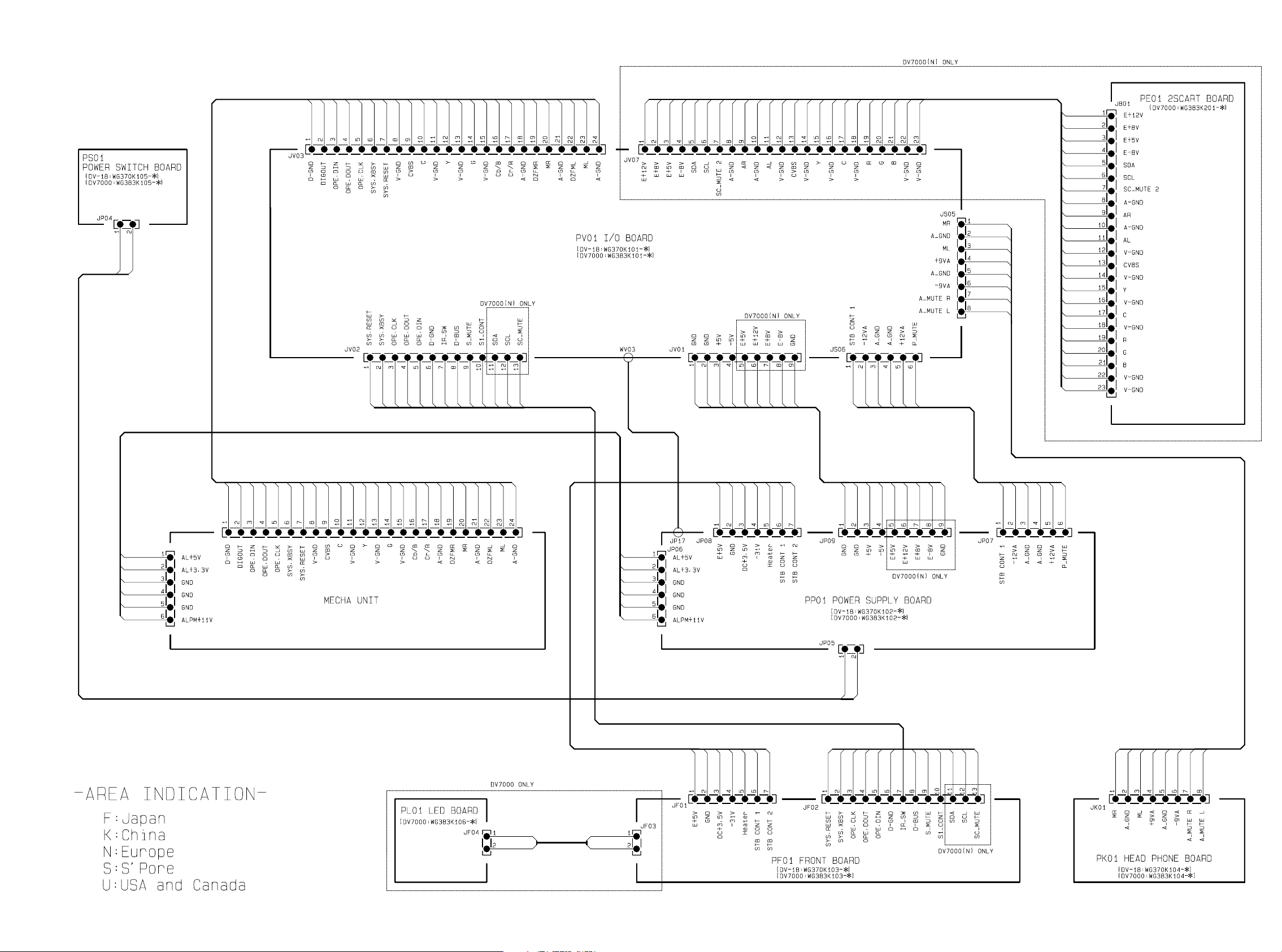
1.10 WIRING DIAGRAM ........................................................................................................................... 1-13
1.11 BLOCK DIAGRAM ............................................................................................................................. 1-15
1.12 SCHEMATIC DIAGRAM .................................................................................................................... 1-17
1.13 PARTS LOCATION ........................................................................................................................... 1-27
1.14 EXPLODED VIEW AND PARTS LIST ............................................................................................... 1-32
1.15 ELECTRICAL PARTS LIST ............................................................................................................... 1-35
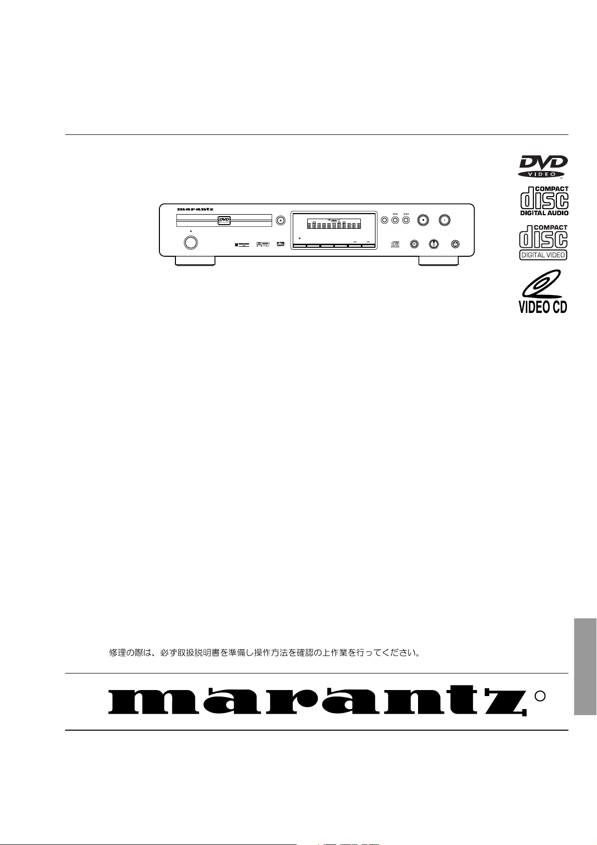
DVD PLAYER DV7000
VIDEO
OPEN/CLOSE
SURROUND
A-B
REPEAT
TITLE
DTS
SHUFFLE
CHAPTER
SVCD
SHUFFLE
CHAPTER
TITLE
TRACK
SCAN
TRACK
TIME
TOTAL
FTS
TRACK
PBC
SCAN
TABLE OF CONTENTS
DVD Player
PLAY
DIMMER
STOP
LEVEL
PAUSE
PHONES
-
+
2. TKM1000MZ ( DVD MODULE for MARANTZ )
2.1 SCHEMATIC DIAGRAM AND PARTS LOCATION ............................................................................. 2-1
2.2 MICROPROCESSOR AND IC DATA ................................................................................................ 2-15
2.3 EXPLODED VIEW AND PARTS LIST ............................................................................................... 2-28
2.4 ELECTRICAL PARTS LIST ............................................................................................................... 2-30
Printed in Japan
Please use this service manual with referring to the user guide ( D.F.U. ) without fail.
DV7000
R
DV7000
383K855010 MIT
3120 785 22300
First Issue 2000.07
Page 2
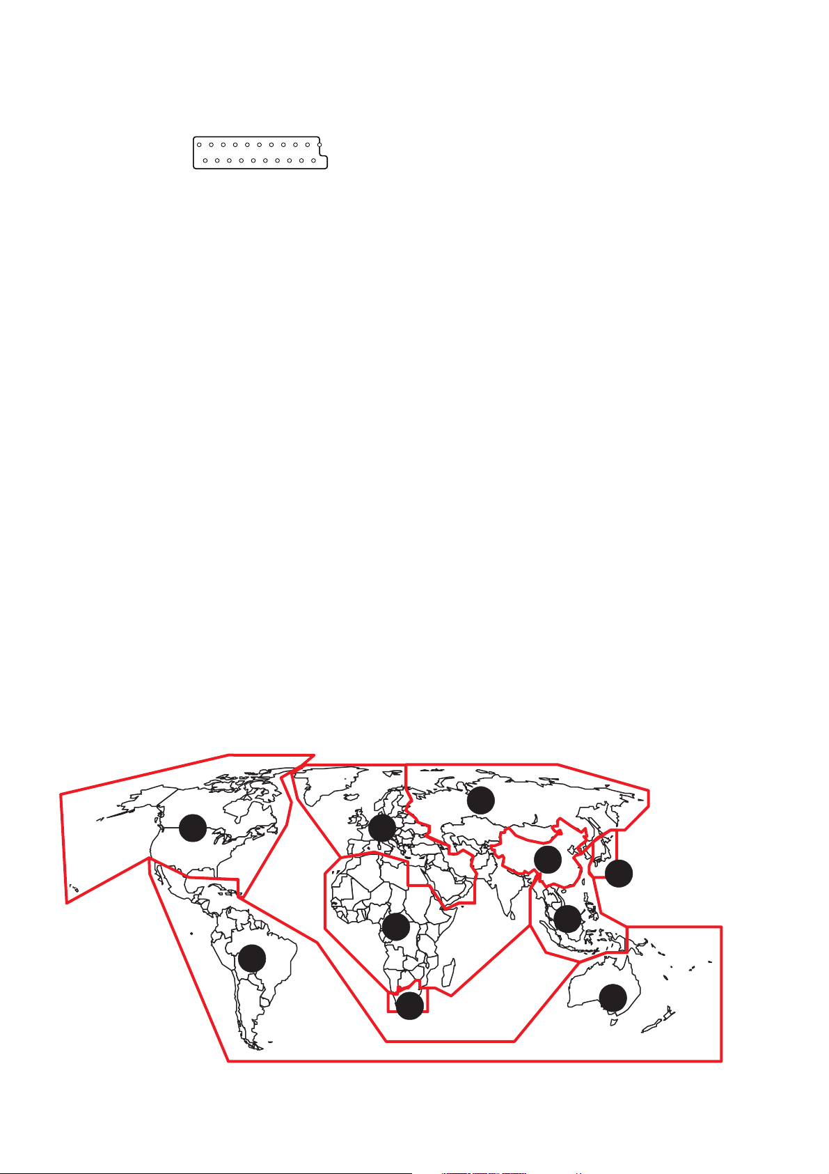
MARANTZ DESIGN AND SERVICE
MARANTZ AMERICA, INC.
WILDASH AUDIO SYSTEMS NZ
Using superior design and selected high grade components, MARANTZ company has created the ultimate in stereo sound.
Only original MARANTZ parts can insure that your MARANTZ product will continue to perform to the specifications for which
it is famous.
Parts for your
MARANTZ equipment are generally available to our National Marantz Subsidiary or Agent.
ORDERING PARTS :
Parts can be ordered either by mail or by Fax.. In both cases, the correct part number has to be specified.
The following information must be supplied to eliminate delays in processing your order :
1. Complete address
2. Complete part numbers and quantities required
3. Description of parts
4. Model number for which part is required
5. Way of shipment
6. Signature : any order form or Fax. must be signed, otherwise such part order will be considered as null and void.
USA
MARANTZ AMERICA, INC
440 MEDINAH ROAD
ROSELLE, ILLINOIS 60172
USA
PHONE : 630 - 307 - 3100
FAX : 630 - 307 - 2687
AMERICAS
SUPERSCOPE TECHNOLOGIES, INC.
MARANTZ PROFESSIONAL PRODUCTS
2640 WHITE OAK CIRCLE, SUITE A
AURORA, ILLINOIS 60504 USA
PHONE : 630 - 820 - 4800
FAX : 630 - 820 - 8103
AUSTRALIA
JAMO AUSTRALIA PTY LTD
1 EXPO COURT, P.O. BOX 350
MT. WAVERLEY VIC 3149
AUSTRALIA
PHONE : +61 - 3 - 9543 - 1522
FAX : +61 - 3 - 9543 - 3677
NEW ZEALAND
WILDASH AUDIO SYSTEMS NZ
14 MALVERN ROAD MT ALBERT
AUCKLAND NEW ZEALAND
PHONE : +64 - 9 - 8451958
FAX : +64 - 9 - 8463554
EUROPE / TRADING
MARANTZ EUROPE B.V.
P.O.BOX 80002, BUILDING SFF2
5600 JB EINDHOVEN
THE NETHERLANDS
PHONE : +31 - 40 - 2732241
FAX : +31 - 40 - 2735578
AUSTRALIA
TECHNICAL AUDIO GROUP PTY, LTD
558 DARLING STREET,
BALMAIN, NSW 2041,
AUSTRALIA
PHONE : 61 - 2 - 9810 - 5300
FAX : 61 - 2 - 9810 - 5355
THAILAND
MRZ STANDARD CO.,LTD
746 - 754 MAHACHAI ROAD.,
WANGBURAPAPIROM, PHRANAKORN,
BANGKOK, 10200 THAILAND
PHONE : +66 - 2 - 222 9181
FAX : +66 - 2 - 224 6795
TAIWAN
PAI- YUING CO., LTD.
6 TH FL NO, 148 SUNG KIANG ROAD,
TAIPEI, 10429, TAIWAN R.O.C.
PHONE : +886 - 2 - 25221304
FAX : +886 - 2 - 25630415
BRAZIL
PHILIP DA AMAZONIA IND. ELET. ITDA
CENTRO DE INFORMACOES AO
CEP 04698-970
SAO PAULO, SP, BRAZIL
PHONE : 0800 - 123123
FAX : +55 11 534. 8988
(Discagem Direta Gratuita)
CANADA
LENBROOK INDUSTRIES LIMITED
633 GRANITE COURT,
PICKERING, ONTARIO L1W 3K1
CANADA
PHONE : 905 - 831 - 6333
FAX : 905 - 831 - 6936
SINGAPORE
WO KEE HONG (S) PTE LTD
WO KEE HONG CENTRE
NO.23, LORONG 8, TOA PAYOH
SINGAPORE 319257
PHONE : +65 2544555
FAX : +65 2502213
MALAYSIA
WO KEE HONG ELECTRONICS SDN. BHD.
SUITE 8.1, LEVEL 8, MENARA GENESIS,
NO. 33, JALAN SULTAN ISMAIL,
50250 KUALA LUMPUR, MALAYSIA
PHONE : +60 3 - 2457677
FAX : +60 3 - 2458180
JAPAN
Technical
MARANTZ JAPAN, INC.
35- 1, 7- CHOME, SAGAMIONO
SAGAMIHARA - SHI, KANAGAWA
JAPAN 228-8505
PHONE : +81 42 748 1013
FAX : +81 42 741 9190
KOREA
MK ENTERPRISES LTD.
ROOM 604/605, ELECTRO-OFFICETEL, 16-58,
3GA, HANGANG-RO, YONGSAN-KU, SEOUL
KOREA
PHONE : +822 - 3232 - 155
FAX : +822 - 3232 - 154
SHOCK, FIRE HAZARD SERVICE TEST :
CAUTION : After servicing this appliance and prior to returning to customer, measure the resistance between either primary AC
cord connector pins ( with unit NOT connected to AC mains and its Power switch ON ), and the face or Front Panel of product and
controls and chassis bottom.
Any resistance measurement less than 1 Megohms should cause unit to be repaired or corrected before AC power is applied, and
verified before it is return to the user/customer.
Ref. UL Standard No. 1492.
In case of difficulties, do not hesitate to contact the Technical
Department at above mentioned address.
991207MIT
Page 3

1. TECHNICAL SPECIFICATIONS
Discs played
DVD video disc ............................................... 12 cm single sided, single layer
Compact disc
(CD-DA, Video CD) ......................................... 12 cm, 8 cm
Video system .................................................... PAL (625/50) / NTSC (525/60)
Audio system ................................................... Linear PCM audio
Video output
Line output level .............................................. 1.0 Vp-p / 75 ohms, unbalanced
S1-output level ................................................. Y output: 1.0 Vp-p / 75 ohms unbalanced
Color different output level ............................... Y output: 1.0 Vp-p / 75 ohms unbalanced
R/G/B output .................................................... R/G/B output: 0.7 Vp-p 21-pin SCART connector x 2 (/N1B)
12 cm single sided, double layer
12 cm double sided, single layer
12 cm double sided, double layer (one layer per side)
8 cm single sided, single layer
8 cm single sided, double layer
8 cm double sided, single layer
8 cm double sided, double layer (one layer per side)
MPEG 1/2 audio
Dolby Digital (AC-3)
DTS audio (Digital output only)
RCA pin Jack x 2
C output: 0.3 Vp-p / 75 ohms (PAL)
0.286 Vp-p / 75 ohms (NTSC)
4 pin mini DIN x 1
CB, CR output: 0.7 Vp-p / 75 ohms
RCA pin Jack x 3 (/F1, /K1, /S1, /U1)
Audio output
Line output ....................................................... 2.0 Vrms / 330 ohms
RCA pin Jack x 2 system
Digital audio output
Optical output ................................................... Optical connector x 1
Coaxial output .................................................. 0.5 Vp-p / 75 ohm RCA pin Jack x 1
DVD Iinear audio characteristics
Frequency response ........................................ 4 Hz-22 kHz (Fs = 48 kHz)
S/N ratio ........................................................... More than 110 dB (Fs = 48 kHz / 24 bit PCM)
Dynamic range ................................................. More than 100 dB (Fs = 48 kHz / 24 bit PCM)
Total harmonic distortion ................................. Less than 0.0025% (Fs = 48 kHz / 24 bit PCM)
4 Hz-44 kHz (Fs = 96 kHz)
CD audio characteristics:
Frequency response ........................................ 4 Hz - 20 kHz (EIAJ)
S/N ratio ........................................................... More than 110 dB (EIAJ)
Dynamic range ................................................. More than 100 dB (EIAJ)
Total harmonic distortion ................................. Less than 0.0025% (EIAJ)
Pickup ............................................................... Wavelength: 655 nm (DVD)
Power requirements ........................................ 120V AC, 60 Hz (/U1)
Power consumption ........................................ 22 W (standby mode = approx 5 W, power off = 0 W)
Operation temperature .................................... 5 °C - 35 °C
Operation humidity range ............................... 5% - 90% (no condensation)
Wavelength: 790 nm (CD)
100V AC, 50 / 60 Hz (/F1)
230V AC, 50 Hz (/N1)
220V AC, 50 Hz (/K1)
220 - 230V AC, 50 / 60 Hz (/S1)
Dimensions ....................................................... 440 (W) x 87 (H) x 304 (D) mm (excluding protrusions)
Weight ............................................................... 4.0 kg
Supplied accessories
Auido / Video cable .......................................... x 1
D-BUS remote cable ........................................ x 1
Remote control unit .......................................... x 1
Batteries ........................................................... x 2
• For improvement purposes, specifications and design are subject to change without notice
1-1
Page 4
2. CONNECTION FACILITIES
2.1 Video performance (/N1 only)
135791113151719
21
2. 1. 1 SCART
2 4 6 8 10 12 14 16 18 20
Pin No. TV (OUT) Pin No. AUX (IN)
Pin 1 Audio R out : 2Vrms Pin 1 Audio R out : 2Vrms
Pin 2 Audio R in : 2Vrms Pin 2 Audio R in : 2Vrms
Pin 3 Audio L out : 2Vrms Pin 3 Audio L out : 2Vrms
Pin 4 GND Pin 4 GND
Pin 5 GND Pin 5 GND
Pin 6 Audio L in : 2Vrms Pin 6 Audio L in : 2Vrms
Pin 7 Blue out/C in Pin 7 Blue in/C out
Pin 8 function switching out <2V : TV Pin 8 function switching in<2V : DVD
Pin 9 GND Pin 9 GND
Pin 10 not connected Pin 10 not connected
Pin 11 Green out:0.7Vpp ±0.1V into 75 Ohm *1 Pin 11 Green in:0.7Vpp ±0.1V into 75 Ohm
Pin 12 not connected Pin 12 not connected
Pin 13 GND Pin 13 GND
Pin 14 GND Pin 14 GND
Pin 15 Red/C out Pin 15 Red/C in
Pin 16 fast switching out <0.4V into 75 Ohm=CVBS/S-Video Pin 16 fast switching in <0.4V into 75 Ohm=CVBS/S-Video
1</<3 into 75 Ohm=RGB 1</<3 into 75 Ohm=RGB
Pin 17 GND Pin 17 GND
Pin 18 GND Pin 18 GND
Pin 19 CVBS/Y out : 1Vpp ±0.1V *1 Pin 19 CVBS/Y out : 1Vpp ±0.1V *1
Pin 20 CVBS/Y in : 1Vpp ±0.1V *1 Pin 20 CVBS/Y in : 1Vpp ±0.1V *1
Pin 21 GND Pin 21 GND
Blue : 0.7Vpp ±0.1V into 75 Ohm *1 Blue : 0.7Vpp ±0.1V into 75 Ohm *1
C : 300mVpp ±30 into 75 Ohm *2 C : 300mVpp ±30 into 75 Ohm *2
>5/<8 : asp.ratio 16 : 9 DVD/AUX >5/<8 : asp.ratio 16 : 9 AUX
>9.5/<12 : asp.ratio 4 : 3 DVD/AUX >9.5/<12 : asp.ratio 4 : 3 AUX
Red : 0.7Vpp ±0.1V into 75 Ohm *1 Red : 0.7Vpp ±0.1V into 75 Ohm *1
C : 300mVpp ±30 into 75 Ohm *2 C : 300mVpp ±30 into 75 Ohm *2
*1 : 100% White *2 : Burst Level *3 : color bar(chroma level : 75%)
What are "regional codes"?
Motion picture studios want to control the home release of movies in different countries because theater releases arenit
simultaneous (a movie may come out on DVD in the US when itis just hitting screens in Europe). Therefore they have
required that the DVD standard include codes which can be used to lock out the playback of certain discs in certain geo-graphical
regions. Players sold in each region will have that regionis code built into the player. The player will refuse to play
these "region coded" discs which are not allowed in the region. However, regional codes are entirely optional. Discs without
codes will play on any player in any country. Some studios have already announced that only their new releases will have
regional codes. There are six regions:
1. United States and Canada 2. Europe and Japan
3. Far East (except Japan & China) 4. South America and Oceania
5. Africa and the Middle East 6. China (except Hong Kong)
5
1 2
6
2
5
3
4
2
Map of DVD Regions
1-2
4
Page 5
3. INFORMATIONS
REGION CODE
VERSION REGION CODE COUNTRY
/FXX 2 JAPAN
/KXX 6 CHINA
/NXX 2 EUROPE
/SXX 3 SINGAPORE/HONGKONG
/UXX 1 USA/CANADA
THE DISCS THAT THE DV7000 CAN HANDLE
The following discs can be played back with a DV7000.
disc mark playback capability size side
DVD Audio/Video
CD Audio
VCD Audio/Video single
Note: The regional code of the discs must meet to the regional
code of the DV7000.
12 cm
8 cm
12 cm
8 cm
12 cm
8 cm
single/double
single
Multi-angles:
On some DVDs, scenes have been filmed from different angles
(up to a maximum of 9). On these discs, you can select the
angle that you want to watch. Please refer to the DVD's manual
to see which scenes have multi-angles.
Cancelling password for parental press the DIMMER button
and hold for 10 seconds while the player is stopped.
DVD INFORMATION
Below is a glossary of the new terms related to DVD.
Title:
A disc may have more than one story/movie on it, so each
story/movie is called a
For example, if there are 2 movies on the disc, they are
separated into Title 1 and Title 2.
Chapter:
A title may also be separated into chapters.
For example, a movie (title) may be separated into 3 scenes
(chapters).
Title 1 Title 2
Chapter1Chapter
2
Subtitles:
DVDs are recorded with up to 32 different subtitle languages.
If a disc has more than one subtitle language, you can select
the subtitle language that you want to read.
"title".
Chapter3Chapter1Chapter2Chapter
3
Soundtrack language:
DVDs are recorded with up to 8 different soundtrack languages.
If a disc has more than one language, you can select the
soundtrack language that you want to listen to.
1-3
Page 6
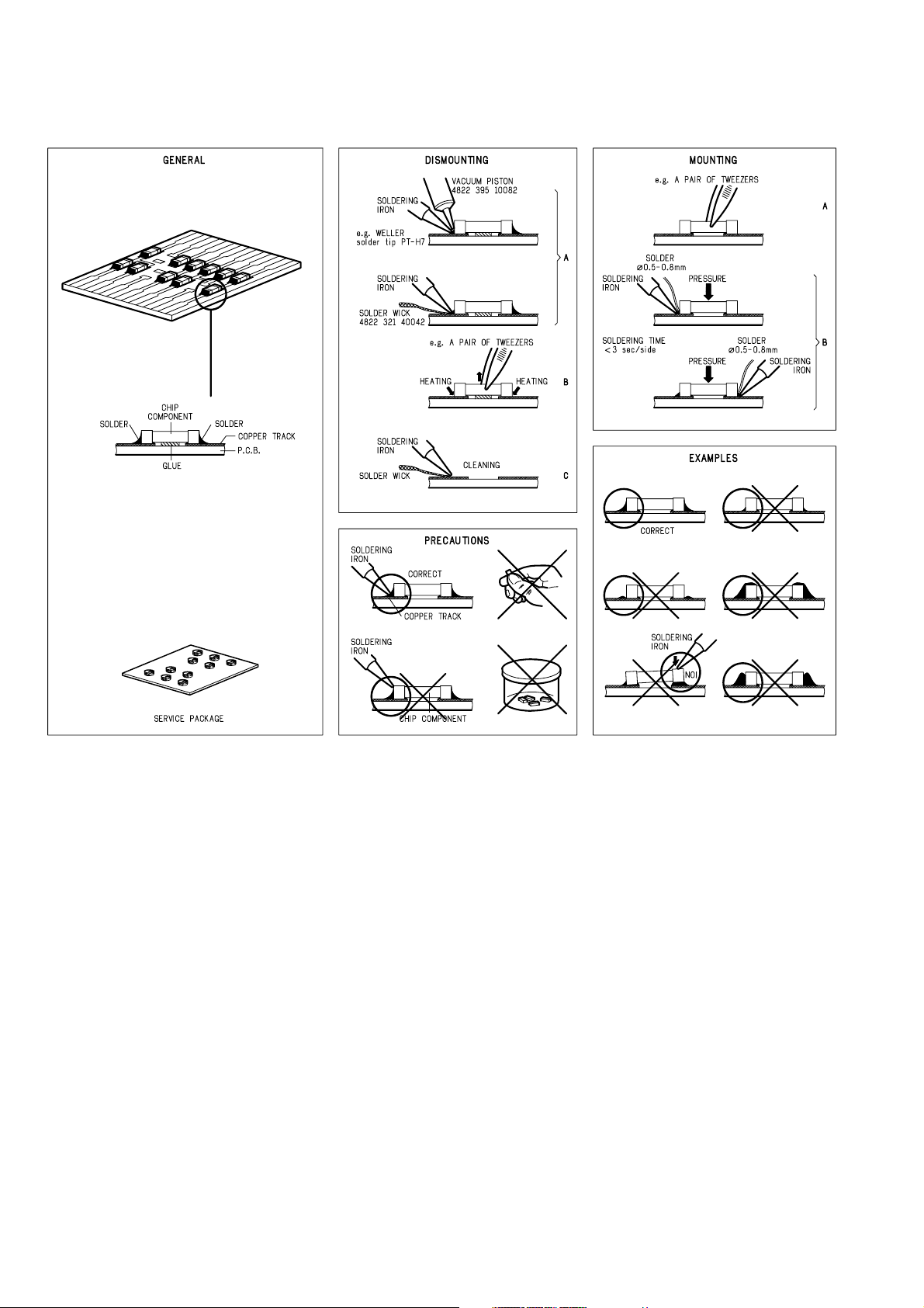
4. SERVICING HINT
SERVICE HINTS
SERVICE TOOLS
Audio signals disc 4822 397 30184
Disc without errors (SBC444)+
Disc with DO errors, black spots and fingerprints (SBC444A) 4822 397 30245
Disc (65 min 1kHz) without no pause 4822 397 30155
Max. diameter disc (58.0 mm) 4822 397 60141
Torx screwdrivers
Set (straight) 4822 395 50145
Set (square) 4822 395 50132
13th order filter 4822 395 30204
DVD test disc (PAL) 4822 397 10131
DVD test disc (NTSC) ALMEDIO TDV-540
1-4
Page 7
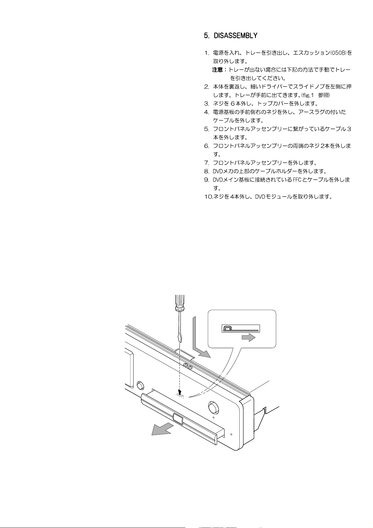
5. DISASSEMBLY
1. Open the tray and remove the escutcheon (050B).
REMARK : If the tray doesn't work, put a small
screwdriver into the hole as shown in picture
and slide the knob. Then the tray comes out.
After the first centimeter it is possible to pull
the tray out by hand. (see fig.1)
2. Remove 6 screws and remove the top cover.
3. Remove a top right side screw on the power supply PCB
and remove the GND lug wire.
4. Remove 3 connectors of the wire harness from (or to )
front panel assembly.
5. Remove 2 screws of left and right side of the front panel
assembly.
6. Remove the front panel assembly.
7. Remove the retainer on the DVD mechanism.
8. Remove FFC and wire harness from the DVD main PCB
which mounted under the DVD mechanism.
9. Remove 4 screws and remove DVD mechanism module.
Fig. 1
1-5
Page 8
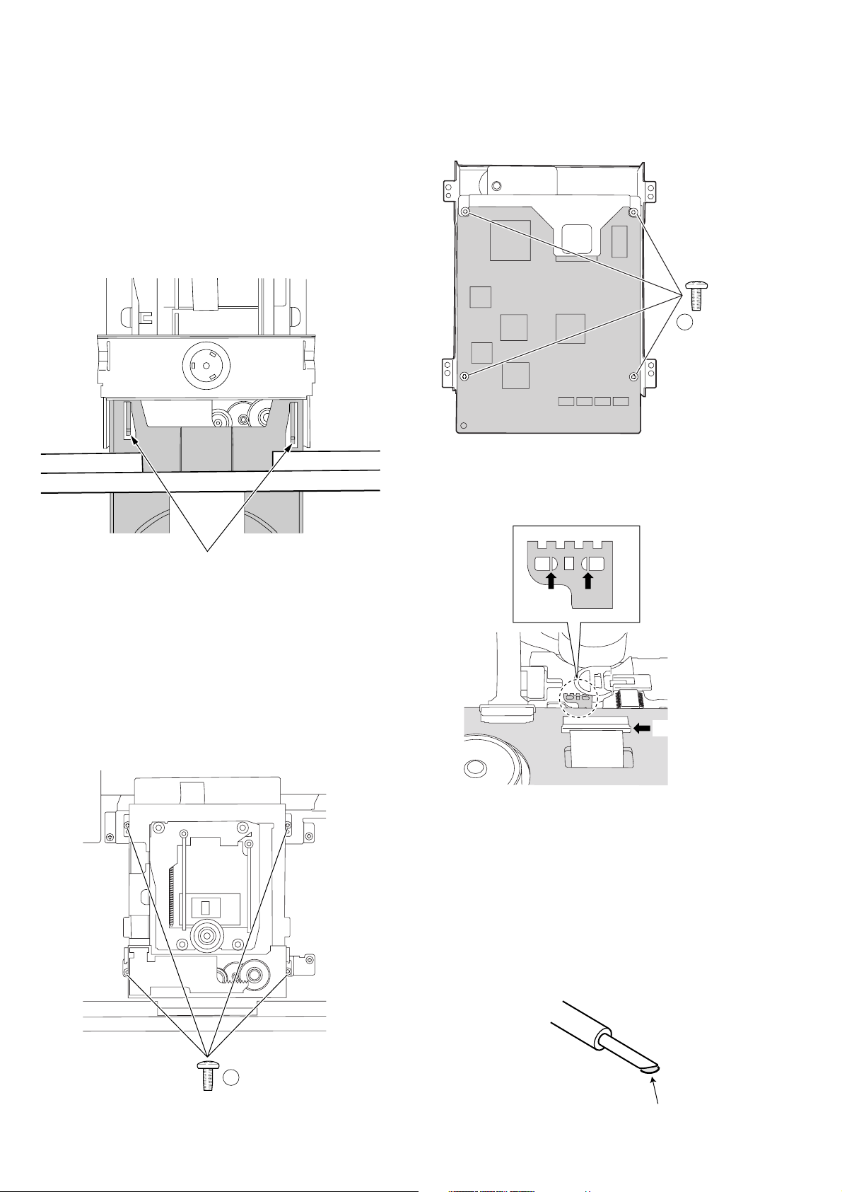
6. REPLACEMENT OF PRINCIPAL COMPONENTS
6-1. Removal of the TRAVERSE MECHA.
6-1-1. Removal of the MECHANISM BLOCK
1) Turn the unit
eject the DISC TRAY.
2) Disconnect the power cord and remove the DISC CLAMPER
BLOCK.
3) Completely remove the DISC TRAY by pulling it outwards
while pulling up both of the stopper tabs alternately.
's power on and press the "EJECT" button to
6-1-2. Removal of the TRAVERSE MECHA.
1) Remove the four b screws on the MAIN PCB and then
disconnect the P800 connector on the MAIN PCB.
B SCREW
Fig. 6-3
2) Short the laser diode protection circuit on the PICK UP
BLOCKÕs flexible cable with solder as shown.
STOPPER TUB
Fig. 6-1
4) Disconnect the two flat cables from the P803 connectors
and one flat cable from the P808 connector on the MAIN
PCB.
5) Disconnect the P807 connector on the MAIN PCB.
6) Remove the four a retaining screws and remove the
MECHANISM BLOCK from the chassis.
P200
Fig. 6-4
Caution
To protect the laser diode from damage caused by high voltage
static electricity, a laser diode protection circuit has to be
shorted before disconnecting the flexible cable (P200 connector
on the MECHANISM PCB). It is recommended that you put
solder on the top of the soldering iron as shown in Fig. 3-5
then short the circuit at once. When you replace the TRAVERSE
MECHA., be sure to connect the P200 connector before
removing the solder at the shorted parts.
Fig. 6-2
A SCREW
SOLDER
Fig. 6-5
1-6
Page 9
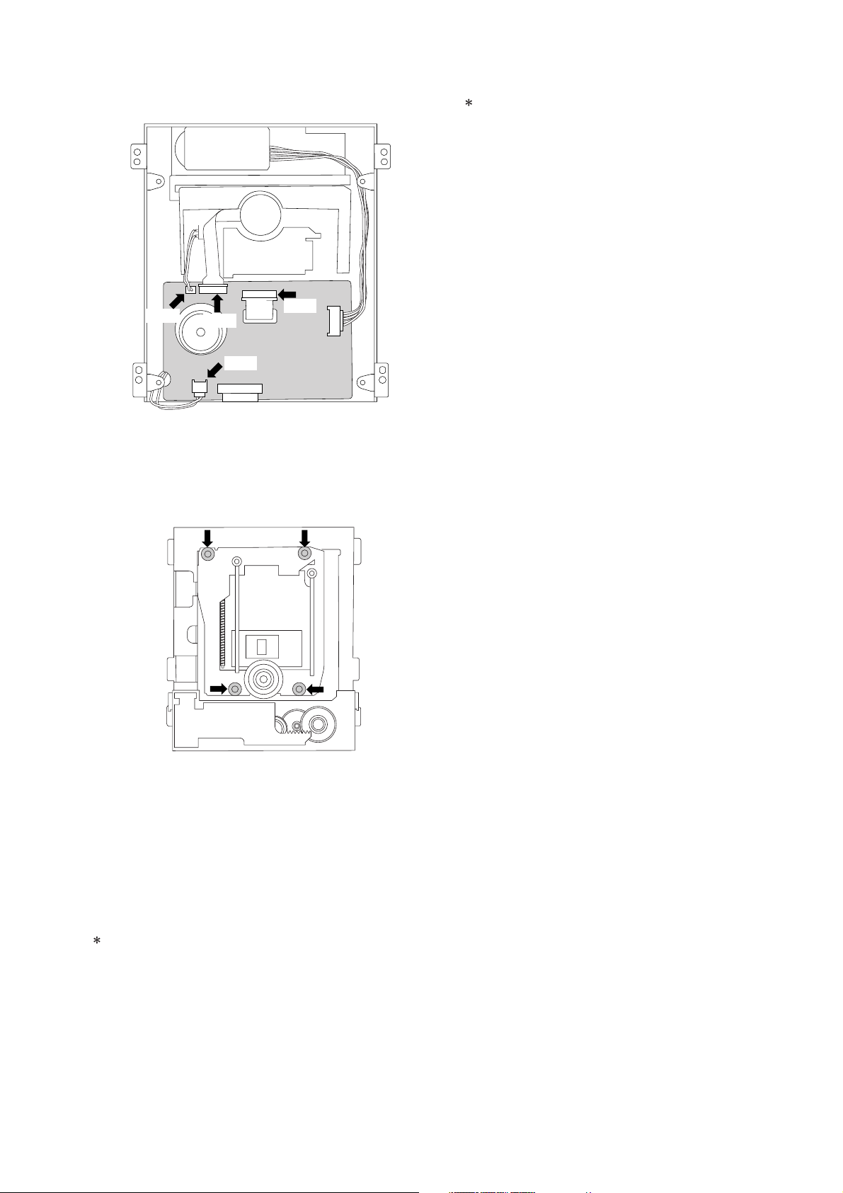
3) Carefully disconnect the two connectors (P500, P600) and
the two flat cables (P200, P300) on the MECHANISM PCB.
6-3. Replacement of the PICK UP BLOCK
Replacement of the PICK UP BLOCK itself is not
recommended because its azimuth adjustment is very
critical and requires a special jig. If PICK UP BLOCK
replacement is necessary, replace with an entire
TRAVERSE MECHANISM only.
P600
P300
P500
P200
Fig. 6-6
4) Using tweezers, release the four retaining HOOKs of the
TRAVERSE MECHA. from the rubber insulators being
careful not to damage the rubber insulators.
Fig. 6-7
5) Remove the TRAVERSE MECHA. from the MECHANISM
BLOCK.
6) Reassemble in the reverse order for installation. Never
remove the solder on the flexible cable before connecting
the P200 connector on the MECHANISM PCB.
6-2. Replacement of the SPINDLE MOTOR
Because the SPINDLE MOTOR position is very critical, jitter
adjustment should be performed after replacement.
1) Disconnect the P300 connector on the MECHANISM PCB.
2) Insert a Philips type screw driver into the hole on the TURN
TABLE of the SPINDLE MOTOR and remove the two
screws.
1-7
Page 10
7. SERVICE MODE
FLD, LED TEST
1. Press the mains switch (POWER BUTTON) while
depressing the PAUSE button and STOP button.
2. Status will be on the TEST mode 1 and FL display shows
<TEST 1>.
3. Press the NEXT button, then Standby LED will be light
ON and FLD shows <LED 1>.
4. Press the NEXT button again, then Surround LED will be
light ON and FLD shows <LED 2>.
5. Press the NEXT button again, then all segments of FLD
will be light ON.
6. Press the NEXT button again, then each segments of
FLD will be light ON by press by press. (17 forms)
7. Finally FLD shows <KEY 0 0 0 0>, it will be in
“BUTTON (KEY) TEST MODE”.
8. If press some button on the front panel, FLD shows a
code of that pressed button.
9. If press the PAUSE button and STOP button
simultaneously while FLD shows <KEY 0 0 0 0>. The
status will be in “REMOTE CONTROL TEST MODE” and
FLD shows <RC6 000000>.
10.If press some button on the remote controller, FLD shows
a code of that pressed button.
11.Press the NEXT button again, then the version number of
the main microprocessor (IC600 on the DVD main PCB)
will be shown on the FLD.
12.Press the NEXT button again, then the version number of
the slave microprocessor (QF01 on the front PCB) will be
shown on the FLD.
13.Press the NEXT button again, then the status will be #2.
<TEST 1> mode. In case of finish the <TEST 1> mode,
press the mains switch (POWER BUTTON).
How to EEPROM all clear
1. Press the mains switch (POWER BUTTON) while
depressing the PLAY button and STOP button.
2. Status will be on the TEST mode 2 and FL display shows
<TEST 2>. After a couple of seconds FL display shows
<TEST2 OK>.
3. Press the PLAY button, PAUSE button and STOP button
simultaneously.
4. FL display shows <TEST OK>, then power off the mains
switch (POWER BUTTON). EEPROM should cleared.
1-8
Page 11
Type version confirmation
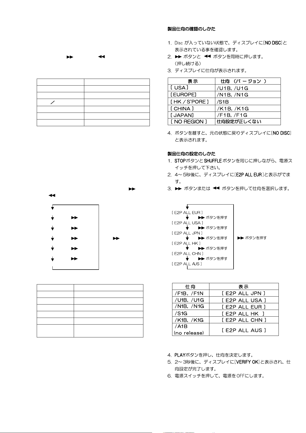
1. Power ON the DVD player. The FL display must be
shown <NO DISC>.
2. Pressing the
button and button simultaneously.
3. FL display shows product versions as follows.
DISPLAY VERSIONS
[ USA ]
[ ]
EUROPE
[ HK S ‘PORE ]
[ CHINA ]
[ J A PAN ]
.
[ NO REGION ]
/U1B, /U1G
/N1B, /N1G
/S1G
/K1B, /K1G
/F1B, /F1N
Incorrect setup.
4. Release buttons. Then FL display shows <NO DISC>
and status will be in usual mode.
Type Version setup
1. Press the mains switch (POWER BUTTON) while
depressing the STOP button and SHUFFLE button.
2. The FL display shows <E2P ALL EUR> after a couple of
seconds.
3. Type versions can be changed by pressing
and
button.
button
[ E2P ALL EUR ]
[ E2P ALL USA ]
[ E2P ALL JPN ]
[ E2P ALL HK ]
[ E2P ALL CHN ]
[ E2P ALL AUS ]
VERSIONS DISPLAY
/F1B, /F1N [ E2P ALL JPN ]
/U1B, /U1G [ E2P ALL USA ]
/N1B, /N1G [ E2P ALL EUR ]
/S1G [ E2P ALL HK ]
/K1B, /K1G [ E2P ALL CHN ]
/A1B
(no release)
4. Memorize the version by pressing PLAY button.
5. The FL display shows <VERIFY OK> after a couple of
seconds.
6. Power OFF the mains switch.
Press button
Press button
Press button
Press button
Press button
Press button
[ E2P ALL AUS ]
1-9
Page 12
8. ELECTRICAL ADJUSTMENT
P807
TP201
TP120
VR120
VR121
P800
TP105
TP107
TP300
VR110
P804 P803
JITTER ADJ
SCREW A
VR202
8-1. DVD JITTER ADJUSTMENT
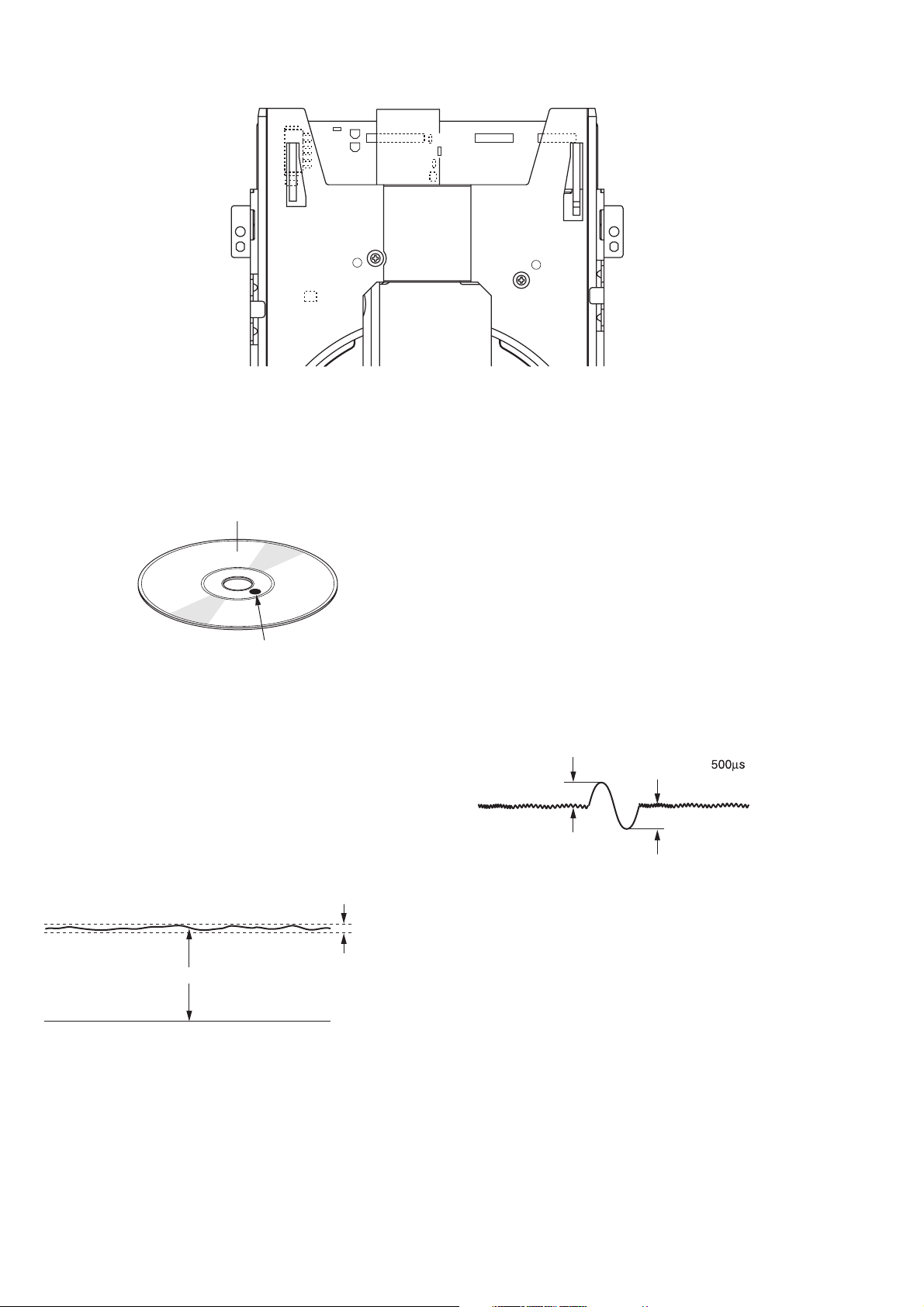
1. Stick the provided small round sticker (0.1 mm thickness) at
the innermost position of a DVD disc as shown and make a
swayed DVD disc.
Signal recorded side
STICKER
Fig. 8-2
2. Play back the swayed DVD disc and press the F.F button
repeatedly until the pickup block reaches the outermost
position of its movable range. Next, press the PAUSE button.
3. Set the oscilloscope to the DC input mode and connect it to
the TP201 (HOT) and the TP102 (D.GND) on the MAIN
PCB.
4. Adjust the a screw and b screw alternately so that the AC
and DC level of the waveform is minimum. (DC level should
be less than 1.8 V, AC component should be minimum.)
JITTER ADJ
SCREW B
Fig. 8-1
2. Set the oscilloscope to the DC input mode and connect it to
the TP201 (HOT) and the TP102 (D.GND) on the MAIN
PCB.
3. Adjust the VR202 so that the DC level is minimum. (The DC
level should be less than 1.8 V)
8-3. CD TRACKING BALANCE
1. Set the VR110 at its center position prior to the adjustment.
2. Connect an oscilloscope to the TP150 (TE) on the MAIN
PCB.
3. Play back an ordinary CD-disc and then set it to the PAUSE
mode. If the play mode does not be engage, turn the VR110
at ±15 degrees. If the play mode does still not be engage
even when the VR110 is turned at ±15 degrees, turn the
VR110 at ± 30 degrees and try it again.
4. Observe the waveform and adjust it so that the level A of the
waveform is the same as level B.
A
B
500mV
Fig. 8-4
minimum
Less than 1.8V
Fig. 8-3
NOTE: If the SPINDLE MOTOR is replaced, this jitter
adjustment should be performed for proper performance.
8-2. SLICE LEVEL ADJUSTMENT
1. Play back an ordinary DVD disc (single side, one layer) and
press the F.F button repeatedly until the pickup block reaches
almost the center position of its movable range.
1-10
Page 13
8-4 AS Adjustment
CAUTION :
Do not see the laser pick-up! Cover the laser pick-up unit
while AS adjustment.
Adjustment point : VR120, VR121
Test point : TP107(+), TP120 (+) TP105 (GND)
Equipment : Digital Multi Meter (DC voltage)
1. Press the mains switch (POWER BUTTON) while depressing
the PLAY button and STOP button.
2. Status will be on the TEST mode 2 and FL display shows
<TEST 2>. After a couple of seconds FL display shows
<TEST2 OK>.
3. Press the
and the status will be in AS adjustment mode.
4. Measure the DC voltage at the test point TP107.
5. Press the
and the FL display shows <E3 00>.
6. Press the button again. Then the CD laser will light ON
and the FL display shows <E3 01>.
7. Adjust the voltage at the test point TP120 by VR121, that the
value must be same as TP107 (10mV) value measured on
#4. process.
8. Press the
light ON and the FL display shows <E3 00>.
9. Measure the DC voltage at the status DVD laser light ON.
Adjust the voltage at that status 35mV (±10mV) lower than
“CD laser light ON “ status by the trim resister VR120.
10.Press the
status CD laser light ON.
(DC voltage must be 35mV higher than the status DVD
laser light ON.)
11.Power OFF the mains switch (POWER BUTTON).
button. Then the FL display shows <E3 02>
button again. Then the DVD laser will light ON
button twice of time. Then the DVD laser will
button again. Confirm the DC voltage at the
1-11
Page 14
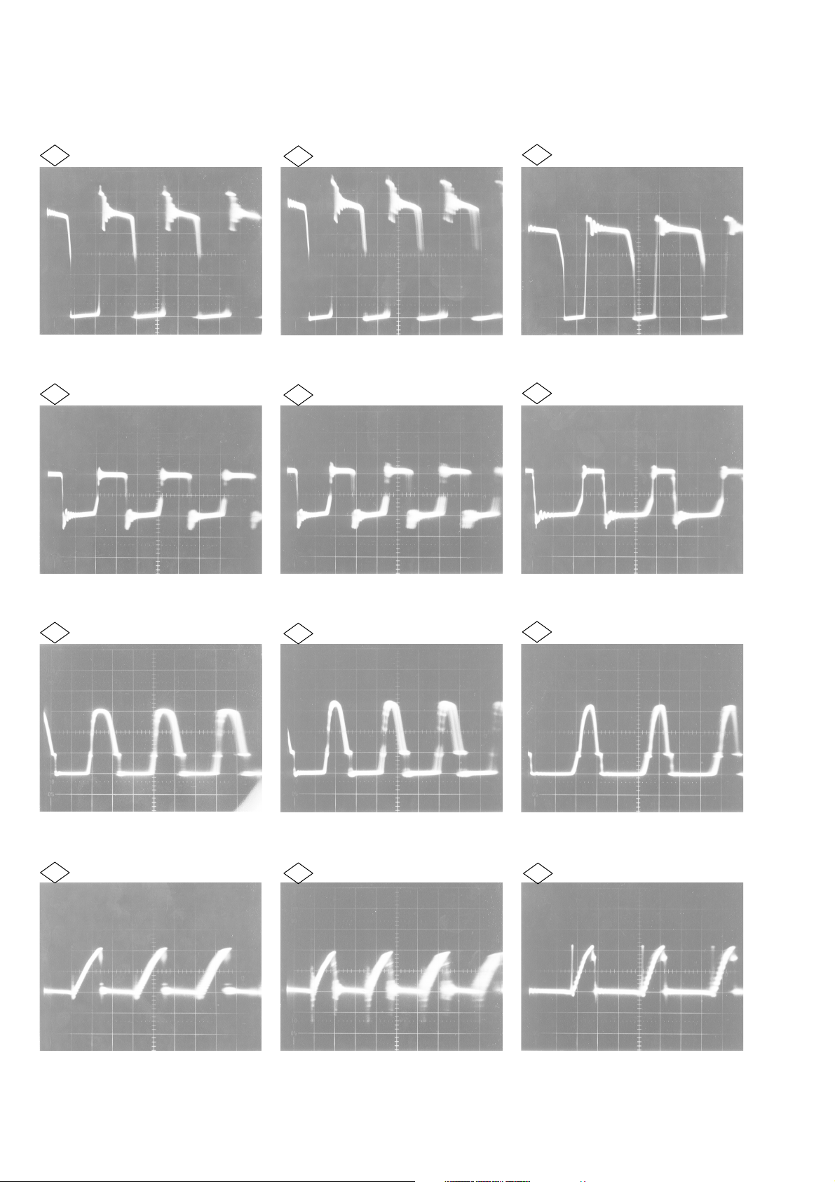
9. WAVEFORM
Power requirements (Refer the circuit diagram page 1-25 and 1-26)
100V AC 120V AV 220V AC
50V 5µsec 50V 5µsec 100V 5µsec
1
2
10V 5µsec 10V 5µsec 10V 5µsec
1
2
1
2
5V 5µsec 5V 5µsec 5V 5µsec
3
0.1V 5µsec 0.1V 5µsec 0.1V 5µsec
4
3
4
3
4
1-12
Page 15
1.10 WARNINGS
1-13 1-14
Page 16
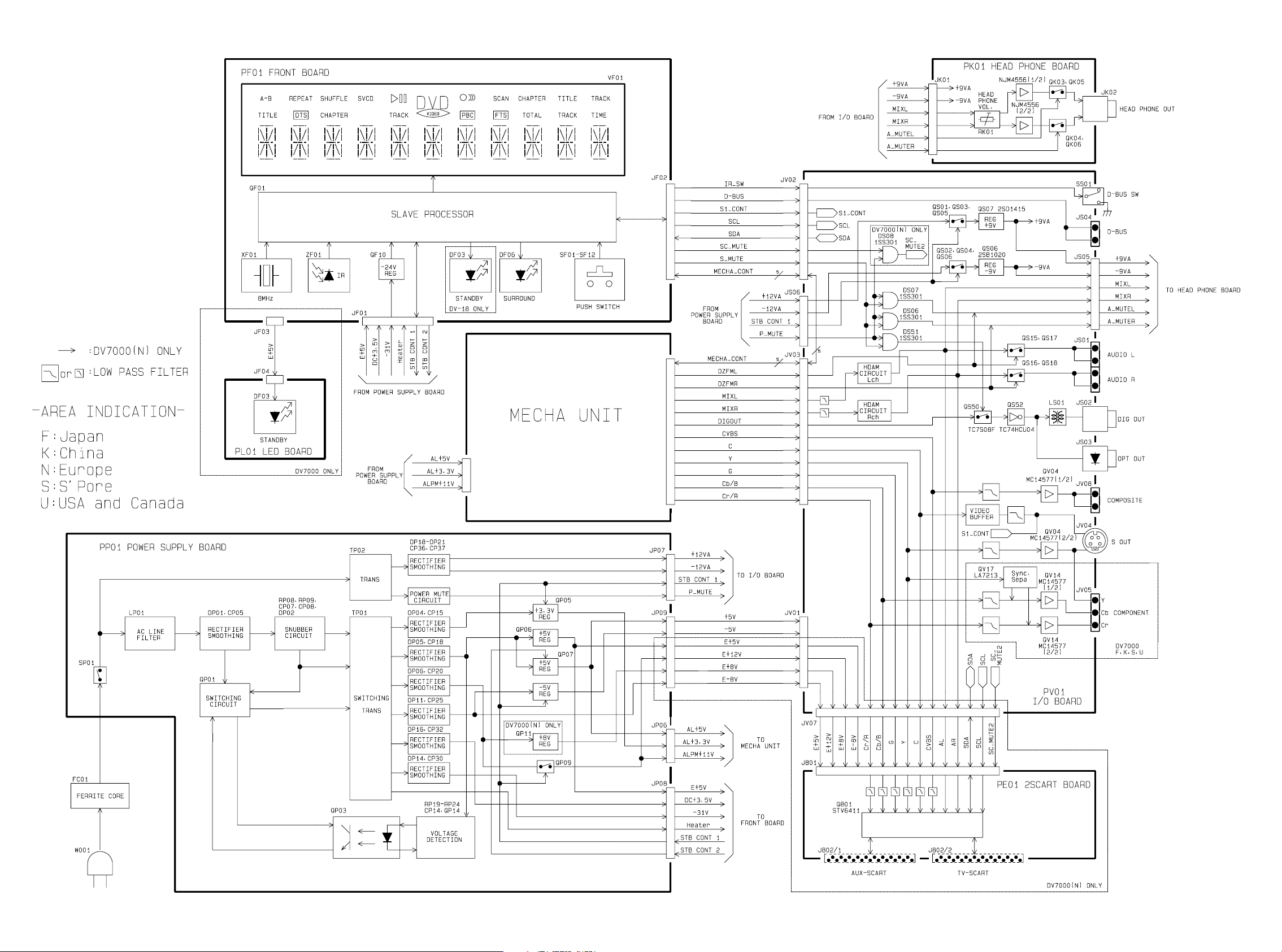
1.11 BLOCK DIAGRAM
1-15 1-16
Page 17
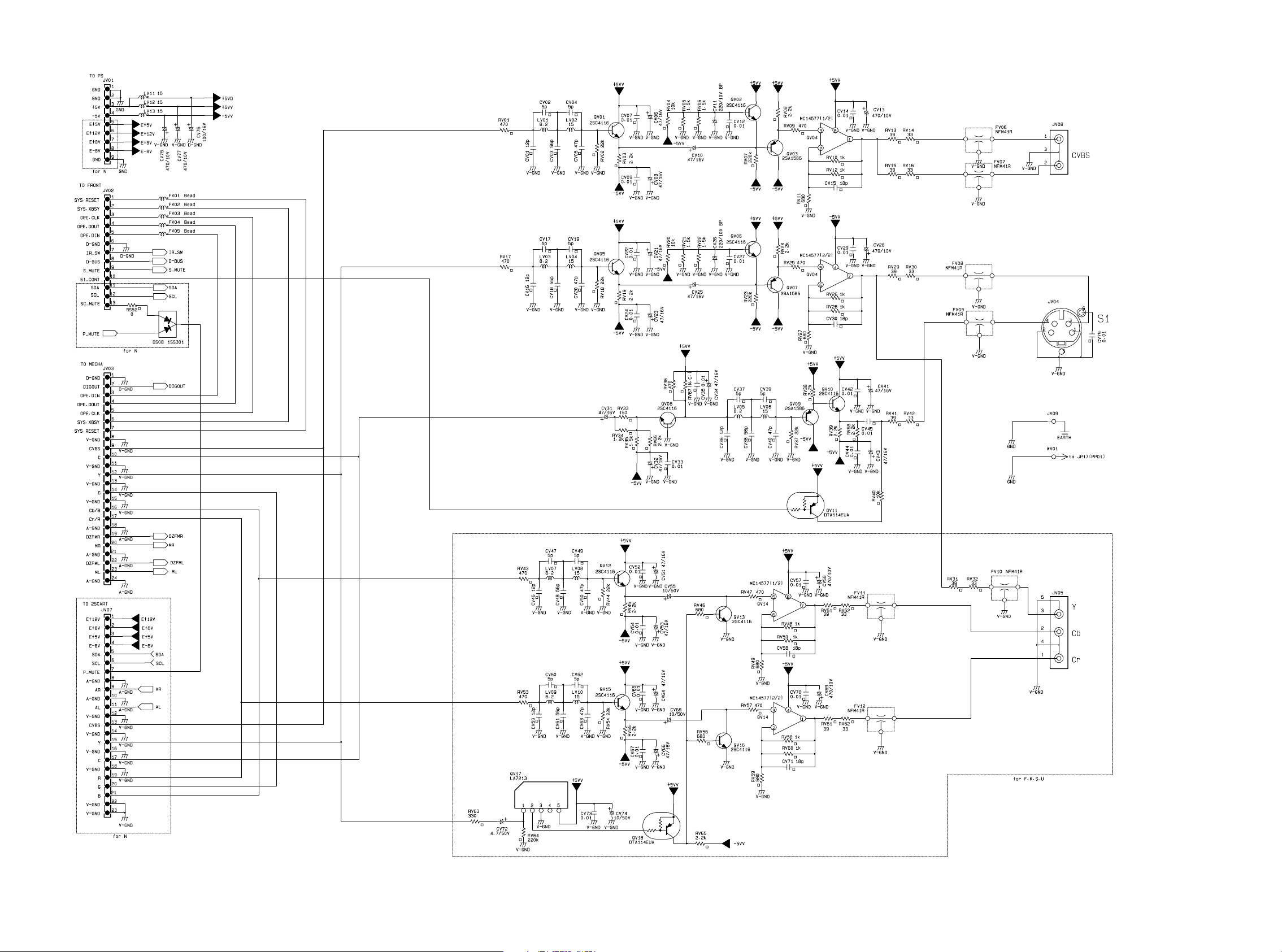
1.12 SCHEMATIC DIAGRAM AND PARTS LOCATION
1-17 1-18
Page 18
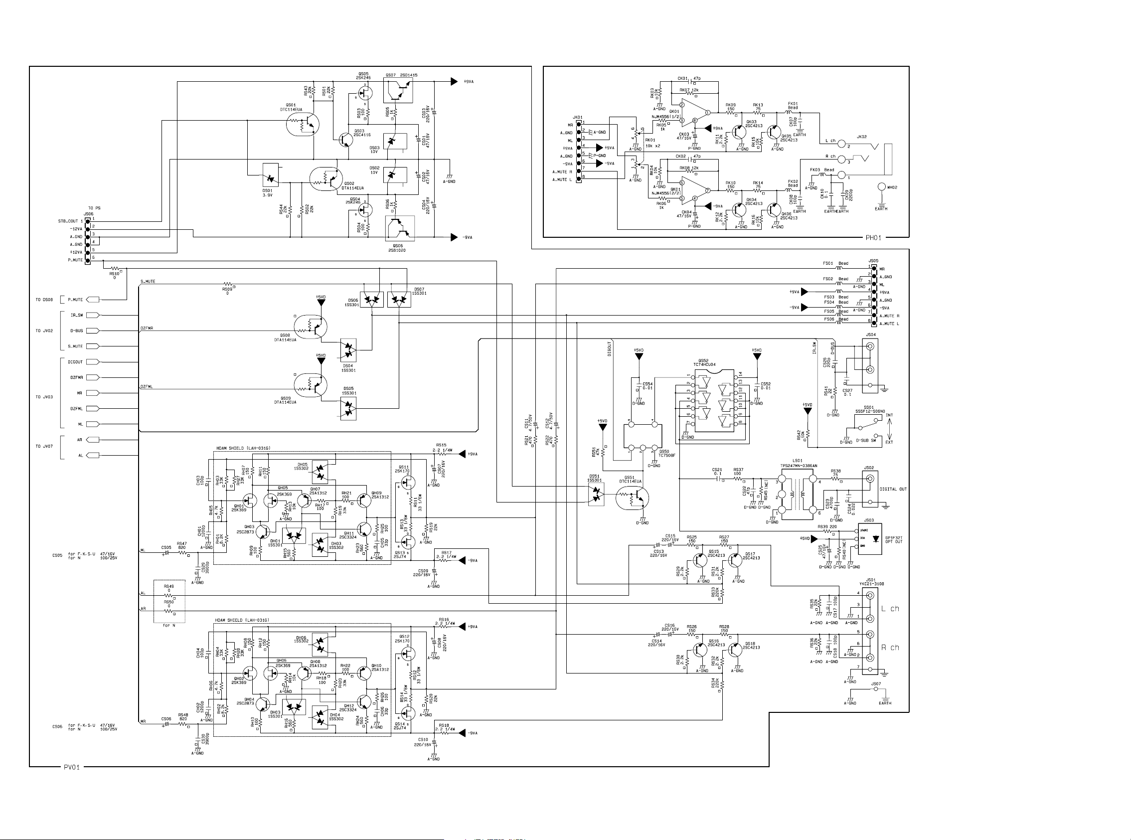
1-19 1-20
Page 19

FBIN_ENC
FBIN_VCR
(see Note 1)
BIN_ENC
BIN_VCR
(see Note 1)
GIN_ENC
GIN_VCR
(see Note 1)
RCIN_ENC
RIN_VCR
(see Note 1)
CIN_ENC
CIN_VCR
CIN_TV
CVBSIN_STB
YCVBSIN_ENC
YCVBSIN_TV
YCVBSIN_VCR
YIN_ENC
LIN_ENC
LIN_STB
LIN_TV
LIN_VCR
RIN_TV
RIN_STB
RIN_ENC
RIN_VCR
FB SWITCH
19
18
46
32
44
30
42
28
40
48
54
34
36
52
50
38
45
41
53
49
56
39
43
47
4V
0V
6d
B
RGB SWITCH
B_ENC
B_ENC
B_VCR
G_ENC
G_VCR
R/C_ENC
R_VCR
MUTE
R/C_ENC
C_ENC
C_VCR
MUTE
CVBS/Y_ENC
CVBS/Y_VCR
CVBS_STB
Y_ENC
MUTE
R/C_ENC
C_ENC
C_TV
MUTE
CVBS_STB
CVBS/Y_ENC
CVBS/Y_TV
Y_ENC
MUTE
VCR SWITCH
L_ENC
L_STB
L_TV
R_ENC
R_STB
R_TV
MUTE
TV SWITCH
L_ENC
L_STB
L_VCR
R_VCR
R_STB
R_ENC
MUTE
C SWITCH
Y/CVBS SWITCH
C SWITCH
Y/CVBS SWITCH
-14dB
-14dB
6d
B
6d
B
6dB
TRAP
6dB
6dB
SLOW BLANK,
6dB
0/6dB
0/6dB
I/O MONITOR
I2C BUS
DECODER
0/6dB
0/6dB
STEREO/
MONO
STEREO/
MONO
STV6411A
17
FBOUT_TV
61
BOUT_TV
63
GOUT_TV
1
RCOUT_TV
9
VOUT_RF
11
FILTER
3
YCVBS/OUT_TV
5
COUT_VCR
7
YCVBSOUT_VCR
25
SLB_TV
27
SLB_VCR
21
SCL
22
SDA
59
LOUT_CINCH
58
ROUT_CINCH
62
LOUT_VCR
60
ROUT_VCR
8
AOUT_RF
2
LOUT_TV
64
ROUT_TV
Q801 STV6411
CC3
CC2
NC
GNDV2
V
NC
FILTER
V
16151413121110
17
FBOUT_TV
FBIN_VCR (see Note 1)
RIN_VCR (see Note 1)
GIN_VCR (see Note 1)
BIN_VCR (see Note 1)
18
19
FBIN_ENC
20
ADD
21
SCL
22
SDA
23
V
CC12
NC
24
SLB_TV
25
NC
26
SLB_VCR
27
28
GNDV1
29
30
NC
31
32
333435363738394041424344454647
CC1
NC
NC
V
YIN_ENC
CVBSIN_STB
YCVBSIN_ENC
Pin Number Symbol Description
1 RCOUT_TV Red/chroma Output, to TV Scart
2 LOUT_TV Audio Left Output, to TV Scart
3 YCVBSOUT_TV Y/CVBS Output, to TV scart
4 NC Not Connected
5 COUT_VCR Chroma Output, to VCR Scart
6 NC Not Connected
7 YCVBSOUT_VCR Y/CVBS Output, to VCR Scart
8 AOUT_RF Audio (L+R) Output to RF Modulator
9 VOUT_RF Video (CVBS) Output to RF Modulator
10 GNDV3 Video Switches Ground 3
11 FILTER Chroma Trap Filter
12 V
13 NC Not Connected
14 GNDV2 Video Switches Ground 2
15 NC Not Connected
16 V
17 FBOUT_TV Fast Blanking Output, to TV Scart
18 FBIN_VCR (see Note 1) Fast Blanking Input, from VCR Scart
19 FBIN_ENC Fast Blanking Input, from Encoder
20 ADD I
21 SCL I
22 SDA I
23 V
24 NC Not Connected
25 SLB_TV Slow Blanking Input/Ouput from TV
26 NC Not Connected
27 SLB_VCR Slow Blanking Input/Ouput from VCR
28 RIN_VCR (see Note 1) Red Input, from VCR Scart
29 GNDV1 Video Switches Ground 1
30 GIN_VCR (see Note 1) Green Input, from VCR Scart
31 NC Not Connected
32 BIN_VCR (see Note 1) Blue Input, from VCR Scart
33 V
34 CVBSIN_STB CVBS Input from STB
35 NC Not Connected
36 YCVBSIN_ENC Y/CVBS Input from Encoder
37 NC Not Connected
38 YIN_ENC Y Input, from Encoder
39 RIN_STB Audio Right Input, from STB
40 CIN_ENC Chroma Input, from Encoder
41 LIN_STB Audio Left Input, from STB
42 RCIN_ENC Red/Chroma Input, from Encoder
43 RIN_ENC Audio Right Input, from Encoder
44 GIN_ENC Green Input, from Encoder
45 LIN_ENC Audio Left Input, from Encoder
46 BIN_ENC Blue Input, from Encoder
47 RIN_VCR Audio Right Input, from VCR Scart
48 CIN_VCR Chroma Input, from VCR Scart
49 LIN_VCR Audio Left Input, from VCR
50 YCVBSIN_VCR Y/CVBS Input from VCR Scart
51 V
52 YCVBSIN_TV Y/CVBS Input, from TV Scart
53 LIN_TV Audio Left Input, from TV Scart
54 CIN_TV Chroma Input, from TV Scart
55 V
56 RIN_TV Audio right input, from TV Scart
57 GNDA Audio Switches Ground
58 ROUT_CINCH Audio Right Output, to CINCH
59 LOUT_CINCH Audio Left Output, to CINCH
60 ROUT_VCR Audio Right Output, to VCR sCart
61 BOUT_TV Blue Output, to TV Scart
62 LOUT_VCR Audio Left Output, to VCR Scart
63 GOUT_TV Green Output, to TV Scart
64 ROUT_TV Audio Right Output, to TV Scart
Notes :
1. Pins (xx_VCR) identified as xx_AU X in STV6410A.
2. In application, all unused pins should be left open or high frequency bypassed to ground.
CCV3
CCV2
CC12
CCV1
REF
CCA
NC
COUT_VCR
NC
YCVBSOUT_VCR
AOUT_RF
VOUT_RF
GNDV3
987654321
LIN_STB
LIN_ENC
RIN_STB
RIN_ENC
CIN_ENC
GIN_ENC
RCIN_ENC
Video Switches Supply 3 (8V)
Video Switches Supply 2 (8V)
2
C Bus IC Address Programmation
2
C Bus Clock
2
C Bus Data
Slow Blanking Power Supply (12V)
Video Switches Supply 1 (8V)
Voltage Reference Decoupling
Audio Switches Supply (8V)
RCOUT_TV
LOUT_TV
YCVBSOUT_TV
48
BIN_ENC
RIN_VCR
CIN_VCR
64
ROUT_TV
63
GOUT_TV
62
LOUT_VCR
61
BOUT_TV
60
ROUT_VCR
59
LOUT_CINCH
58
ROUT_CINCH
GNDA
57
RIN_TV
56
V
55
CCA
54
CIN_TV
53
LIN_TV
52
YCVBSIN_TV
51
V
REF
50
YCVBSIN_VCR
49
LIN_VCR
1-21 1-22
Page 20

A-B
TITLE
SHUFFLE
REPEAT
CHAPTER
VCD
TRACK
PBC
SCAN
FTS
TITLE
CHAPTER
TRACK
TOTAL
TRACK
TIME
1-23 1-24
Page 21

1-25 1-26
Page 22

PS01
1.13 PARTS LOCATION
PF01
QF08 QF11 QF01
QF06 QF07 QF05 QF10
QF04
QF09 QF03 QF02 QF12
PL01
PP01
QP18 QP19
QP20 - QP22
QP02
QP01
QP25
QP03
QP24
QP04 QP12 QP14 QP13
QP13 QP11
QP05 QP07
QP09 QP08 QP06
QP10
PK01
QK03 QK05
QK01 QK04 QK06
1-27 1-28
Page 23

QS04 QS02 QS01 QS03 QS05 QS07
QH02 - QH12
(Even number)
QH03 - QH11
(Odd number)
QV10 QV05 QV08 QV15
QV03 QV02
QV07 QV06
QV09 QV10 QV16 QV13
QV12
QV17 QV18
QS08 QS09
QS14 QS12 QS11 QS13QS15 - QS18 QV04 QV11 QV14 QV18 QS51 QS50
QS52
1-29 1-30
Page 24

1.14 EXPLODED VIEW AND PARTS LIST
POS.
NO
VERS.
COLOR
PART NO.
(FOR PCS)
DESCRIPTION
PART NO.
(MJI)
PE01
Q952 - Q955
Q960-Q962
Q956 - Q959 Q823 Q819 - Q821
Q808
Q809
Q801
Q814
Q815 - Q818
Q802 Q803 Q804 Q805 Q806 Q807
001B BLACK 9965 000 05014 FRONT CHASSIS PL(L)BLK 383K105010
001B GOLD 9965 000 05015 FRONT CHASSIS PL(L)GLD 383K105110
002B BLACK 9965 000 05016 FRONT CHASSIS PL(R)BLK 383K105020
002B GOLD 9965 000 05017 FRONT CHASSIS PL(R)GLD 383K105120
003B BLACK 9965 000 05018 FRONT PANEL AL DV7000 BL 383K248010
003B GOLD 9965 000 05019 FRONT PANEL AL DV7000 GL 383K248110
005B BLACK 9965 000 05020 BUTTON FUNCTION BLK 383K270010
005B GOLD 9965 000 05021 BUTTON FUNCTION GLD 383K270110
006B BLACK 9965 000 05022 BUTTON OPEN/CLOSE BLK 383K270020
006B GOLD 9965 000 05023 BUTTON OPEN/CLOSE GLD 383K270120
007B 9965 000 05024 WINDOW DV7000 383K158010
008B 9965 000 05025 BUTTON SUB FUNCTION 386K270090
009B 4822 454 11825 MARANTZ BADGE (BL) 185J251010
010B 9965 000 01393 LENS STANDBY 312J355010
020B BLACK 4822 411 20336 KNOB PHONE BLACK 284T154310
020B GOLD 9965 000 00580 KNOB PHONE GOLD 284T154240
045B BLACK 9965 000 01975 BUTTON POWER BLACK 255W270010
045B GOLD 9965 000 01395 BUTTON POWER GOLD 255W270110
050B BLACK 9965 000 05026 ESCUTCHEON
050B GOLD 9965 000 05027 ESCUTCHEON
051B BLACK 9965 000 05028 DVD BADGE BLK 386K251030
051B GOLD 9965 000 05029 DVD BADGE GLD 386K251130
009G 9965 000 05030 LEG
010G 9965 000 05031 LEG
025G 9965 000 00362 LINK,POWER SW. 349K121010
911G /F BUSHING MAINS CORD 318K259020
911G /K, /S
/N, /U
001A 9965 000 04619 DVD MODULE UNIT
WV01 9965 000 04963 FFC MECHA- AV YU24075510
WV02 /N 9965 000 04965 FFC AV-2SCART YU23135520
W001 /F MAINS CORD 15A 125V
W001 /K1B MAINS CORD
W001 /K1G MAINS CORD CCEE
W001 /S, /N 4822 321 11343 MAINS CORD YC01800790
W001 /U MAINS CORD UL/CSA
PACKING
001T /F USER GUIDE 383K851110
001T /K, /S USER GUIDE 383K851350
001T /N 9965 000 05032 USER GUIDE 383K851320
001T /U USER GUIDE 383K851310
001Z 9965 000 05013 REMOTE COMMANDER
NOT STANDARD SPARE
001S PACKING CASE DV7000 383K801010
002S CUSHION 386K809010
4822 532 60948 BUSHING MAINS CORD 450H259010
TRAY FRONT BLK
TRAY FRONT GLD
(GOLD HOT STAMP) F
(GOLD HOT STAMP) R
DVD MECHA+DIGITAL BOARD
OFC HANAI
FOR BS(MAYOR)
APP.(AC250V 10A)+ VAR2P
NON-INTEGRAL
RC7000DV
PARTS
383K063010
383K063110
383K057010
383K057110
ZK370K0100
YC01800430
YC01800760
YC01800880
YC02000880
ZK383K0010
1-31 1-32
Page 25

NVERSION
SY MBOL ST YL E
5110
5126
5127
5128
5129
54 05
001Z
PA RT S NA ME
+B.H.M.SCREW
+B. H. T AP T I TE SCREW W/WASHER
+ P. H. T AP T I T E SC REW ( B T YPE )
+ B. H. T AP T I T E SC REW ( B T YPE )
+ B. H. T AP T I T E SCREW( W / T . L . WAS HER )
TOOT HE D L OCK WASHERS
T
E
X
T
00 1B
5129
3X8( M)
01 5B x 3
003B
010B
51 2 8
3X8 ( M)
009B
MARK MATERI AL/FINISH
( M) ST EE L / COPPER
(U) STEEL/BLACK
045B
006B
007B
04 1B
025 G
PL01
VF 0 1
00 8B
002B
5126
3X8( M)
055B
056B
005B
PF 0 1
00 1D
05 1 B
001A
050B
02 1B
02 6 G
5126
3x 8( M)
51 28
3x 8( M)
PK0 1
51 2 8
3X8 ( M)
020G
5126
3X8( M)
056 G
02 1 G
003G
007Gx4
51 29
3X8( M)
5128
3x 8( M)
5128
3X8( M)
009G
51 1 0
3x 6 ( M)
PE 0 1
51 28
3x 8 ( M)
5110
3x 6( M)
L002
L
5128
3X8 ( M)
FC0 1
PS0 1
51 10
3x 6( M)
5128
3X8( M)
5129
3X8( M)
990G
UONLY
901G
5110
3x 6( M)
034G
NONLY
L0 04
L003
I
N
V
I
A
V
S
O
I
I
B
D
L
E
D
I
R
L
E
A
C
S
T
E
R
E
X
R
P
O
A
S
D
U
I
R
A
E
T
I
T
O
O
N
B
E
A
M
.
055G x 2
51 2 7
3x 8 ( M)
W001
911G
N, K ONL Y
990G
511 0
3x 6( M)
5127
3x 8( M)
PV0 1
L0 0 5
L001
PP 0 1
031G x 2
5110
3x 8( M)
51 28
3x 8( M)
TP 0 1
54 0 5
3( M)
048G
033G
99 1G
032G x 3
NONLY
043G x 2
035G
00 1 G
W
H
E
N
O
P
E
N
.
036G
002 G
5129
3X8( M)
042G x 2
NONLY
010Gx2
020B
5128
3x 8( M)
1-33 1-34
009G
Page 26

1.15 ELECTRICAL PARTS LIST
ASSIGNMENT OF COMMON PARTS CODES.
RESISTORS
R : 1) GD05 × × × 140, Carbon film fixed resistor, ±5% 1/4W
R : 2) GD05 × × × 160, Carbon film fixed resistor, ±5% 1/6W
Examples ;
Resistance value
➀
0.1 Ω .... 001 10 Ω .... 100 1 kΩ .... 102 100 kΩ .... 104
0.5 Ω .... 005 18 Ω .... 180 2.7 kΩ .... 272 680 kΩ .... 684
1 Ω .... 010 100 Ω .... 101 10 kΩ .... 103 1 MΩ .... 105
6.8 Ω .... 068 390 Ω .... 391 22 kΩ .... 223 4.7 MΩ .... 475
Note : Please distinguish 1/4W from 1/6W by the shape of parts
used actually.
CAPACITORS
C : CERAMIC CAP.
3) DD1 × × × × 370, Ceramic capacitor
Examples ;
Tolerance (Capacity deviation)
➁
±0.25 pF .... 0
Tolerance of COMMON PARTS handled here are as follows :
C : CERAMIC CAP.
Examples ;
C : 5) ELECTROLY CAP. ( ), 6) FILM CAP. ( )
Examples ;
Examples ;
NOTE
0.5 pF 5 pF .... ±0.25 pF
12 pF 560 pF .... ±5%
Capacity value
➂
0.5 pF .... 005 3 pF .... 030 100 pF .... 101
1.5 pF .... 015 47 pF .... 470 560 pF .... 561
4) DK16 × × × 300, High dielectric constant ceramic
Capacity value
➃
100 pF .... 101 1000 pF .... 102 10000 pF .... 103
470 pF .... 471 2200 pF .... 222
5) EA
Capacity value
➄
0.1 µF .... 104 4.7 µF .... 475 100 µF ....107
0.33 µF .... 334 10 µF .... 106 330 µF ....337
Working voltage
➅
6) DF15 × × × 350 Plastic film capacitor
DF15 × × × 310 One-way type, Mylar ±5% 50V
DF16 × × × 310 Plastic film capacitor
Capacity value
➆
0.001 µF (1000 pF) ....... 102 0.1 µF .... 104
0.0018 µF ........................ 182 0.56 µF ....564
0.01 µF ........................ 103 1 µF ....105
0.015 µF ........................ 153
: 1) The above CODES ( R , R , C , C and
C ) are omitted on the schematic diagram in some
case.
2) On the occasion, be confirmed the common parts on
the parts list.
3) Refer to “Common Parts List” for the other common
parts (RI05, DD4, DK4).
{
➀
{
➁
±0.5 pF .... 1
±5% .... 5
6 pF 10 pF .... ±0.5 pF
1 pF .... 010 10 pF .... 100 220 pF .... 221
➃
× × × × ×
{
➄
1 µF....105 22 µF ....226 1100 µF ....118
6.3V .... 006 25V .... 025
10V .... 010 35V .... 035
16V .... 016 50V .... 050
➆
Resistance value
➂
{
➅
{
Disc type
Temp.coeff.P350 N1000, 50V
Capacity value
Tolerance
capacitor
Disc type
Temp.chara. 2B4, 50V
Capacity value
×
10, Electrolytic capacitor
{
One-way lead type, Tolerance ±20%
Working voltage
Capacity value
One-way type, Mylar ±10% 50V
Capacity value
2200 µF ....228
NOTE ON SAFETY FOR FUSIBLE RESISTOR :
The suppliers and their type numbers of fusible resistors
are as follows;
1. KOA Corporation
Part No. (MJI) Type No. (KOA) Description
NH05 × × × 140 RF25S × × × × ΩJ(±5% 1/4W)
NH05 × × × 120 RF50S × × × × ΩJ(±5% 1/2W)
NH85 × × × 110 RF73B2A × × × × ΩJ(±5% 1/10W)
NH95 × × × 140 RF73B2E × × × × ΩJ(±5% 1/4W)
2. Matsushita Electronic Components Co., Ltd
Part No. (MJI) Type No. (MEC) Description
NF05 × × × 140 ERD-2FCJ × × × (±5% 1/4W)
RF05 × × × 140
NF02 × × × 140
RF02 × × × 140
Examples ;
{
Resistance value
ERD-2FCG
{
Resistance value
Resistance value
0.1 Ω .... 001 10 Ω .... 100 1 kΩ .... 102 100 kΩ .... 104
0.5 Ω .... 005 18 Ω .... 180 2.7 kΩ .... 272 680 kΩ .... 684
1 Ω .... 010 100 Ω .... 101 10 kΩ .... 103 1 MΩ .... 105
6.8 Ω .... 068 390 Ω .... 391 22 kΩ .... 223 4.7 MΩ .... 475
{
Resistance value
(0.1 Ω − 10 kΩ)
× × × (±2% 1/4W)
{
Resistance value
ABBREVIATION AND MARKS
ANT. : ANTENNA BATT. : BATTERY
CAP. : CAPACITOR CER. : CERAMIC
CONN. : CONNECTING DIG. : DIGITAL
HP : HEADPHONE MIC. : MICROPHONE
µ-PRO : MICROPROCESSOR REC. : RECORDING
RES. : RESISTOR SPK : SPEAKER
SW : SWITCH TRANSF. : TRANSFORMER
TRIM. : TRIMMING TRS. : TRAMSISTOR
VAR. : VARIABLE X’TAL : CRYSTAL
NOTE ON SAFETY :
Symbol Fire or electrical shock hazard. Only original
parts should be used to replaced any part marked with
symbol . Any other component substitution (other
than original type), may increase risk of fire or electrical
shock hazard.
VERS.
POS.
COLOR
NO
PE01- SCART CIRCUIT
PE01-CAPACITORS
C802 /N 4822 124 90354 ELECT. 100µF M 16V RA-2 OA10701620
C804 /N 4822 124 90354 ELECT. 100µF M 16V RA-2 OA10701620
C806 /N 4822 126 11663 CER. CHIP 12pF ±5% CG 50V DD95120300
C808 /N 4822 122 33782 CER. CHIP 56pF DD95560300
C810 /N 4822 122 33777 CER. CHIP 47pF ±5% CG 50V DD95470300
C812 /N 4822 126 11663 CER. CHIP 12pF ±5% CG 50V DD95120300
C814 /N 4822 122 33782 CER. CHIP 56pF DD95560300
C816 /N 4822 122 33777 CER. CHIP 47pF ±5% CG 50V DD95470300
C819 /N 4822 126 11703 CER. CHIP 0.01µF DK98103300
C821 /N 9965 000 04997 CER. CHIP 5pF ±0.25pF CH DD90050300
C823 /N 4822 122 33741 CER. CHIP 10pF ±0.5pF CH DD91100300
C825 /N 4822 126 11704 CER. CHIP 0.022µF DK98223300
C827 /N 4822 126 11663 CER. CHIP 12pF ±5% CG 50V DD95120300
C829 /N 4822 122 33782 CER. CHIP 56pF DD95560300
C831 /N 4822 126 13956 CER. CHIP 68pF DD95680300
C833 /N 4822 126 11703 CER. CHIP 0.01µF DK98103300
C835 /N 9965 000 04997 CER. CHIP 5pF ±0.25pF CH DD90050300
C836 /N 4822 122 33782 CER. CHIP 56pF DD95560300
C838 /N 4822 126 13956 CER. CHIP 68pF DD95680300
C840 /N 4822 126 11703 CER. CHIP 0.01µF DK98103300
C842 /N 9965 000 04997 CER. CHIP 5pF ±0.25pF CH DD90050300
C844 /N 4822 122 33741 CER. CHIP 10pF ±0.5pF CH DD91100300
C846 /N 5322 124 21731 ELECT. 10µF M 50V RA-2 OA10605020
C848 /N 4822 126 11703 CER. CHIP 0.01µF DK98103300
C850 /N 4822 122 33777 CER. CHIP 47pF ±5% CG 50V DD95470300
C852 /N 4822 126 11703 CER. CHIP 0.01µF DK98103300
C854 /N 4822 126 11704 CER. CHIP 0.022µF DK98223300
C856 /N 4822 126 11703 CER. CHIP 0.01µF DK98103300
C858 /N 4822 126 11703 CER. CHIP 0.01µF DK98103300
C860 /N 4822 126 11703 CER. CHIP 0.01µF DK98103300
C862 /N 4822 126 11703 CER. CHIP 0.01µF DK98103300
C865 /N 4822 126 11703 CER. CHIP 0.01µF DK98103300
C869 /N 4822 126 11703 CER. CHIP 0.01µF DK98103300
C871 /N 4822 126 11703 CER. CHIP 0.01µF DK98103300
C876 /N 4822 126 13883 CER. CHIP 220pF ±5% CG 50V DD95221300
C881 /N 4822 126 13883 CER. CHIP 220pF ±5% CG 50V DD95221300
C884 /N 4822 126 11687 CER. CHIP 0.1µF DK98104200
C887 /N 4822 126 11687 CER. CHIP 0.1µF DK98104200
C951 /N 4822 124 90354 ELECT. 100µF M 16V RA-2 OA10701620
C953 /N 4822 124 80067 ELECT. 4.7µF M 50V RA-2 OA47505020
C956 /N 4822 124 80067 ELECT. 4.7µF M 50V RA-2 OA47505020
C960 /N 4822 124 80067 ELECT. 4.7µF M 50V RA-2 OA47505020
C962 /N 4822 126 13883 CER. CHIP 220pF ±5% CG 50V DD95221300
C964 /N 4822 124 80067 ELECT. 4.7µF M 50V RA-2 OA47505020
C968 /N 4822 124 80067 ELECT. 4.7µF M 50V RA-2 OA47505020
C970 /N 4822 126 13883 CER. CHIP 220pF ±5% CG 50V DD95221300
C972 /N 4822 124 41539 ELECT. 47µF 16V OA47601620
C975 /N 5322 126 11578 CER. CHIP 1000pF DK96102300
C977 /N 5322 126 11578 CER. CHIP 1000pF DK96102300
PE01-RESISTORS
R801 /N 4822 051 30101 CHIP 100Ω ±5% 1/16W NN05101610
R802 /N 4822 051 30681 CHIP 680Ω ±5% 1/16W NN05681610
R803 /N 4822 051 30471 CHIP 470Ω ±5% 1/16W NN05471610
R804 /N 4822 051 30472 CHIP 4.7kΩ ±5% 1/16W NN05472610
R805 /N 4822 051 30101 CHIP 100Ω ±5% 1/16W NN05101610
R806 /N 4822 051 30681 CHIP 680Ω ±5% 1/16W NN05681610
R807 /N 4822 051 30471 CHIP 470Ω ±5% 1/16W NN05471610
R808 /N 4822 051 30472 CHIP 4.7kΩ ±5% 1/16W NN05472610
R809 /N 4822 051 30101 CHIP 100Ω ±5% 1/16W NN05101610
R810 /N 4822 051 30681 CHIP 680Ω ±5% 1/16W NN05681610
R811 /N 4822 051 30471 CHIP 470Ω ±5% 1/16W NN05471610
R812 /N 4822 051 30472 CHIP 4.7kΩ ±5% 1/16W NN05472610
R813 /N 4822 051 30101 CHIP 100Ω ±5% 1/16W NN05101610
R814 /N 4822 051 30681 CHIP 680Ω ±5% 1/16W NN05681610
PART NO.
(FOR PCS)
DESCRIPTION
BOARD [ /N VERSION ]
PART NO.
(MJI)
1-35 1-36
VERS.
POS.
COLOR
NO
R815 /N 4822 051 30471 CHIP 470Ω ±5% 1/16W NN05471610
R816 /N 4822 051 30472 CHIP 4.7kΩ ±5% 1/16W NN05472610
R817 /N 4822 051 30101 CHIP 100Ω ±5% 1/16W NN05101610
R818 /N 4822 051 30681 CHIP 680Ω ±5% 1/16W NN05681610
R819 /N 4822 051 30471 CHIP 470Ω ±5% 1/16W NN05471610
R820 /N 4822 051 30472 CHIP 4.7kΩ ±5% 1/16W NN05472610
R821 /N 4822 051 30101 CHIP 100Ω ±5% 1/16W NN05101610
R822 /N 4822 051 30681 CHIP 680Ω ±5% 1/16W NN05681610
R823 /N 4822 051 30471 CHIP 470Ω ±5% 1/16W NN05471610
R824 /N 4822 051 30472 CHIP 4.7kΩ ±5% 1/16W NN05472610
R825 /N 4822 051 30101 CHIP 100Ω ±5% 1/16W NN05101610
R826 /N 4822 051 30101 CHIP 100Ω ±5% 1/16W NN05101610
R827 /N 4822 051 30472 CHIP 4.7kΩ ±5% 1/16W NN05472610
R828 /N 4822 051 30472 CHIP 4.7kΩ ±5% 1/16W NN05472610
R829 /N 4822 051 30222 CHIP 2.2kΩ ±5% 1/16W NN05222610
R830 /N 4822 051 30472 CHIP 4.7kΩ ±5% 1/16W NN05472610
R831 /N 4822 051 30472 CHIP 4.7kΩ ±5% 1/16W NN05472610
R832 /N 4822 117 13632 CHIP 100kΩ ±5% 1/16W NN05104610
R833 /N 4822 051 30561 CHIP 560Ω ±5% 1/16W NN05561610
R834 /N 4822 051 30562 CHIP 5.6kΩ ±5% 1/16W NN05562610
R835 /N 4822 051 30102 CHIP 1kΩ ±5% 1/16W NN05102610
R836 /N 4822 116 82487 CHIP 0Ω ±5% 1/16W NN05000610
R837 /N 4822 117 12925 CHIP 47kΩ ±5% 1/16W NN05473610
R838 /N 4822 051 30471 CHIP 470Ω ±5% 1/16W NN05471610
R839 /N 4822 051 30121 CHIP 120Ω ±5% 1/16W NN05121610
R840 /N 4822 051 30151 CHIP 150Ω ±5% 1/16W NN05151610
R841 /N 4822 051 30102 CHIP 1kΩ ±5% 1/16W NN05102610
R842 /N 4822 051 30151 CHIP 150Ω ±5% 1/16W NN05151610
R843 /N 4822 051 30221 CHIP 220Ω ±5% 1/16W NN05221610
R844 /N 4822 051 30102 CHIP 1kΩ ±5% 1/16W NN05102610
R845 /N 4822 051 30472 CHIP 4.7kΩ ±5% 1/16W NN05472610
R846 /N 4822 051 30102 CHIP 1kΩ ±5% 1/16W NN05102610
R847 /N 4822 051 30472 CHIP 4.7kΩ ±5% 1/16W NN05472610
R849 /N 4822 117 13632 CHIP 100kΩ ±5% 1/16W NN05104610
R850 /N 4822 051 30561 CHIP 560Ω ±5% 1/16W NN05561610
R851 /N 4822 051 30562 CHIP 5.6kΩ ±5% 1/16W NN05562610
R852 /N 4822 051 30472 CHIP 4.7kΩ ±5% 1/16W NN05472610
R853 /N 4822 116 82487 CHIP 0Ω ±5% 1/16W NN05000610
R854 /N 4822 117 12925 CHIP 47kΩ ±5% 1/16W NN05473610
R855 /N 4822 051 30471 CHIP 470Ω ±5% 1/16W NN05471610
R856 /N 4822 051 30121 CHIP 120Ω ±5% 1/16W NN05121610
R857 /N 4822 051 30151 CHIP 150Ω ±5% 1/16W NN05151610
R858 /N 4822 051 30472 CHIP 4.7kΩ ±5% 1/16W NN05472610
R859 /N 4822 051 30151 CHIP 150Ω ±5% 1/16W NN05151610
R860 /N 4822 051 30221 CHIP 220Ω ±5% 1/16W NN05221610
R861 /N 4822 117 11817 CHIP 1.2kΩ ±5% 1/16W NN05122610
R862 /N 4822 117 11817 CHIP 1.2kΩ ±5% 1/16W NN05122610
R863 /N 4822 051 30471 CHIP 470Ω ±5% 1/16W NN05471610
R864 /N 4822 051 30101 CHIP 100Ω ±5% 1/16W NN05101610
R865 /N 4822 051 30471 CHIP 470Ω ±5% 1/16W NN05471610
R866 /N 4822 051 30121 CHIP 120Ω ±5% 1/16W NN05121610
R867 /N 4822 051 30151 CHIP 150Ω ±5% 1/16W NN05151610
R868 /N 4822 051 30101 CHIP 100Ω ±5% 1/16W NN05101610
R869 /N 4822 051 30471 CHIP 470Ω ±5% 1/16W NN05471610
R870 /N 4822 051 30121 CHIP 120Ω ±5% 1/16W NN05121610
R871 /N 4822 051 30151 CHIP 150Ω ±5% 1/16W NN05151610
R872 /N 4822 051 30101 CHIP 100Ω ±5% 1/16W NN05101610
R873 /N 4822 051 30471 CHIP 470Ω ±5% 1/16W NN05471610
R874 /N 4822 051 30151 CHIP 150Ω ±5% 1/16W NN05151610
R875 /N 4822 051 30221 CHIP 220Ω ±5% 1/16W NN05221610
R876 /N 4822 051 30221 CHIP 220Ω ±5% 1/16W NN05221610
R877 /N 4822 051 30101 CHIP 100Ω ±5% 1/16W NN05101610
R878 /N 4822 051 30471 CHIP 470Ω ±5% 1/16W NN05471610
R879 /N 4822 051 30121 CHIP 120Ω ±5% 1/16W NN05121610
R880 /N 4822 051 30151 CHIP 150Ω ±5% 1/16W NN05151610
R881 /N 4822 051 30181 CHIP 180Ω ±5% 1/16W NN05181610
R882 /N 4822 051 30151 CHIP 150Ω ±5% 1/16W NN05151610
PART NO.
(FOR PCS)
DESCRIPTION
PART NO.
(MJI)
Page 27

POS.
NO
VERS.
COLOR
PART NO.
(FOR PCS)
DESCRIPTION
PART NO.
(MJI)
POS.
NO
VERS.
COLOR
PART NO.
(FOR PCS)
DESCRIPTION
PART NO.
(MJI)
R883 /N 4822 051 30471 CHIP 470Ω ±5% 1/16W NN05471610
R884 /N 4822 117 12925 CHIP 47kΩ ±5% 1/16W NN05473610
R885 /N 4822 051 30181 CHIP 180Ω ±5% 1/16W NN05181610
R886 /N 4822 051 30151 CHIP 150Ω ±5% 1/16W NN05151610
R887 /N 4822 051 30181 CHIP 180Ω ±5% 1/16W NN05181610
R888 /N 4822 051 30151 CHIP 150Ω ±5% 1/16W NN05151610
R889 /N 4822 116 83829 CHIP 270Ω ±5% 1/16W NN05271610
R890 /N 4822 116 83829 CHIP 270Ω ±5% 1/16W NN05271610
R891 /N 4822 051 30221 CHIP 220Ω ±5% 1/16W NN05221610
R892 /N 4822 051 30101 CHIP 100Ω ±5% 1/16W NN05101610
R893 /N 4822 051 30471 CHIP 470Ω ±5% 1/16W NN05471610
R894 /N 4822 051 30121 CHIP 120Ω ±5% 1/16W NN05121610
R895 /N 4822 051 30151 CHIP 150Ω ±5% 1/16W NN05151610
R896 /N 4822 051 30181 CHIP 180Ω ±5% 1/16W NN05181610
R897 /N 4822 051 30151 CHIP 150Ω ±5% 1/16W NN05151610
R898 /N
R903 /N
R904 /N 4822 051 30102 CHIP 1kΩ ±5% 1/16W NN05102610
R905 /N 4822 051 30102 CHIP 1kΩ ±5% 1/16W NN05102610
R906 /N
R909 /N
R951 /N 4822 051 30474 CHIP 470kΩ ±5% 1/16W NN05474610
R952 /N 4822 051 30471 CHIP 470Ω ±5% 1/16W NN05471610
R953 /N 4822 051 30471 CHIP 470Ω ±5% 1/16W NN05471610
R954 /N 4822 117 12925 CHIP 47kΩ ±5% 1/16W NN05473610
R955 /N 4822 117 12925 CHIP 47kΩ ±5% 1/16W NN05473610
R956 /N 4822 051 30151 CHIP 150Ω ±5% 1/16W NN05151610
R957 /N 4822 051 30151 CHIP 150Ω ±5% 1/16W NN05151610
R958 /N 4822 051 30222 CHIP 2.2kΩ ±5% 1/16W NN05222610
R959 /N 4822 051 30222 CHIP 2.2kΩ ±5% 1/16W NN05222610
R960 /N 4822 051 30151 CHIP 150Ω ±5% 1/16W NN05151610
R961 /N 4822 051 30151 CHIP 150Ω ±5% 1/16W NN05151610
R962 /N 4822 051 30222 CHIP 2.2kΩ ±5% 1/16W NN05222610
R963 /N 4822 051 30222 CHIP 2.2kΩ ±5% 1/16W NN05222610
R964 /N 4822 051 30223 CHIP 22kΩ ±5% 1/16W NN05223610
R965 /N 4822 051 30223 CHIP 22kΩ ±5% 1/16W NN05223610
R968 /N 4822 051 30471 CHIP 470Ω ±5% 1/16W NN05471610
R969 /N 4822 051 30471 CHIP 470Ω ±5% 1/16W NN05471610
R970 /N 4822 117 12925 CHIP 47kΩ ±5% 1/16W NN05473610
R971 /N 4822 117 12925 CHIP 47kΩ ±5% 1/16W NN05473610
R972 /N 4822 051 30151 CHIP 150Ω ±5% 1/16W NN05151610
R973 /N 4822 051 30151 CHIP 150Ω ±5% 1/16W NN05151610
R974 /N 4822 051 30222 CHIP 2.2kΩ ±5% 1/16W NN05222610
R975 /N 4822 051 30222 CHIP 2.2kΩ ±5% 1/16W NN05222610
R976 /N 4822 051 30151 CHIP 150Ω ±5% 1/16W NN05151610
R977 /N 4822 051 30151 CHIP 150Ω ±5% 1/16W NN05151610
R978 /N 4822 051 30222 CHIP 2.2kΩ ±5% 1/16W NN05222610
R979 /N 4822 051 30222 CHIP 2.2kΩ ±5% 1/16W NN05222610
R980 /N 4822 051 30223 CHIP 22kΩ ±5% 1/16W NN05223610
R981 /N 4822 051 30223 CHIP 22kΩ ±5% 1/16W NN05223610
R984 /N 4822 051 30471 CHIP 470Ω ±5% 1/16W NN05471610
R985 /N 4822 051 30471 CHIP 470Ω ±5% 1/16W NN05471610
R986 /N 4822 117 12925 CHIP 47kΩ ±5% 1/16W NN05473610
R987 /N 4822 117 12925 CHIP 47kΩ ±5% 1/16W NN05473610
R988 /N 4822 051 30103 CHIP 10kΩ ±5% 1/16W NN05103610
R989 /N 4822 051 30222 CHIP 2.2kΩ ±5% 1/16W NN05222610
R990 /N 4822 051 30103 CHIP 10kΩ ±5% 1/16W NN05103610
PE01-SEMICONDUCTORS
D801 /N 4822 130 83715 CHIP DIODE 1SS301 DAN202U HZ21005000
D802 /N 4822 130 80346 CHIP DIODE 02CZ8.2 HZ30004050
D803 /N 4822 130 80346 CHIP DIODE 02CZ8.2 HZ30004050
D805 /N 4822 130 80346 CHIP DIODE 02CZ8.2 HZ30004050
D807 /N 4822 130 80346 CHIP DIODE 02CZ8.2 HZ30004050
D808 /N 4822 130 80346 CHIP DIODE 02CZ8.2 HZ30004050
D809 /N 4822 130 80346 CHIP DIODE 02CZ8.2 HZ30004050
/N 4822 051 30221 CHIP 220Ω ±5% 1/16W NN05221610
/N 4822 051 30151 CHIP 150Ω ±5% 1/16W NN05151610
D810 /N 4822 130 80346 CHIP DIODE 02CZ8.2 HZ30004050
Q801 /N 9965 000 05001 IC STV6411A
Q802
Q807 2SA1576 (Q R)
Q808 /N 4822 130 60669 CHIP TRS. 2SC4081 (Q R)
Q809 /N 4822 130 60669 CHIP TRS. 2SC4081 (Q R)
Q810 /N 4822 130 10698 CHIP TRS. 2SA1586 (Y GR)
Q811
Q814 2SC4116 (Y GR)
Q815 /N 4822 130 10698 CHIP TRS. 2SA1586 (Y GR)
Q816
Q823 2SC4116 (Y GR)
Q952
Q959
Q960 /N 4822 130 60669 CHIP TRS. 2SC4081 (Q R)
Q961 /N 4822 130 60669 CHIP TRS. 2SC4081 (Q R)
Q962 /N 4822 130 61903 DIG.TRS. DTA114EU BA10026210
PE01-MISCELLANEOUS
F801 /N 9965 000 04998 EMI FILTER NFM41R01C221 FM31221020
F802 /N 4822 051 30121 CHIP 120Ω ±5% 1/16W NN05121610
F803
F808
F809 /N 4822 051 30121 CHIP 120Ω ±5% 1/16W NN05121610
F810
F814
F952 /N 4822 051 30471 CHIP 470Ω ±5% 1/16W NN05471610
F953 /N 4822 051 30471 CHIP 470Ω ±5% 1/16W NN05471610
F954 /N 4822 051 30121 CHIP 120Ω ±5% 1/16W NN05121610
F955 /N 4822 051 30121 CHIP 120Ω ±5% 1/16W NN05121610
F956 /N 4822 051 30471 CHIP 470Ω ±5% 1/16W NN05471610
F957 /N 4822 051 30471 CHIP 470Ω ±5% 1/16W NN05471610
F958 /N 4822 051 30121 CHIP 120Ω ±5% 1/16W NN05121610
F959 /N 4822 051 30121 CHIP 120Ω ±5% 1/2W NN05121610
J801 /N 9965 000 04999 JACK FFC 23FMN-BTRK(ST) YJ07019470
J802 /N 9965 000 05000 TERMINAL YKF41-5019
L801
L804 COIL 15µH J%
L805 /N 9965 000 00458 CHOKE COIL 8.2µH EL0405 LC18223900
L806 /N 4822 157 60445 CHOKE COIL 15µH J% LC11533900
L807 /N 9965 000 00458 CHOKE COIL 8.2µH EL0405 LC18223900
L808 /N 4822 157 60445 CHOKE COIL 15µH J% LC11533900
L809 /N 9965 000 00458 CHOKE COIL 8.2µH EL0405 LC18223900
L810 /N 4822 157 60445 CHOKE COIL 15µH J% LC11533900
L811 /N 9965 000 00458 CHOKE COIL 8.2µH EL0405 LC18223900
L812 /N 4822 157 60445 CHOKE COIL 15µH J% LC11533900
L813 /N 9965 000 00458 CHOKE COIL 8.2µH EL0405 LC18223900
L814 /N 4822 157 60445 CHOKE COIL 15µH J% LC11533900
L815 /N 9965 000 00458 CHOKE COIL 8.2µH EL0405 LC18223900
L816 /N 4822 157 60445 CHOKE COIL 15µH J% LC11533900
L951 /N 4822 157 60445 CHOKE COIL 15µH J% LC11533900
/N 4822 130 10698 CHIP TRS. 2SA1586 (Y GR) HX100012A0
/N 4822 130 60669 CHIP TRS. 2SC4081 (Q R) HX300012A0
/N 4822 130 60669 CHIP TRS. 2SC4081 (Q R) HX300012A0
/N 4822 130 63601 CHIP TRS. 2SC4213 HX342132A0
/N 9965 000 04998 EMI FILTER NFM41R01C221 FM31221020
/N 9965 000 04998 EMI FILTER NFM41R01C221 FM31221020
/N 4822 157 60445 CHOKE COIL SUBSTITUDE LC11533900
A/V SWITCH MATRIX
2SC4116 (Y GR)
2SC4116 (Y GR)
2SA1576A (Q R)
2SA1576A (Q R)
2SC4116 (Y GR)
2SC4116 (Y GR)
EUROCONNECTOR(21X2)
HC10008540
HX300012A0
HX300012A0
HX100012A0
HX100012A0
HX300012A0
HX300012A0
YT02420010
37
Page 28

POS.
NO
VERS.
COLOR
PART NO.
(FOR PCS)
DESCRIPTION
PART NO.
(MJI)
POS.
NO
VERS.
COLOR
PART NO.
(FOR PCS)
DESCRIPTION
PART NO.
(MJI)
PF01-FRONT CIRCUIT BOARD
PF01-CAPACITORS
CF01
CF11
CF12 4822 124 23056 ELECT CAP. 47µF 10V EJ47601010
CF13 9965 000 01912 CER. CHIP 0.047µF DK98473300
CF14 9965 000 01912 CER. CHIP 0.047µF DK98473300
CF15 9965 000 01912 CER. CHIP 0.047µF DK98473300
CF16 /N 4822 122 31765 CER. CHIP 100pF ±5% CG 50V DD95101300
CF17 /N 4822 122 31765 CER. CHIP 100pF ±5% CG 50V DD95101300
CF19 9965 000 01912 CER. CHIP 0.047µF DK98473300
CF21 4822 124 23056 ELECT CAP. 47µF 10V EJ47601010
CF22 4822 126 11703 CER. CHIP 0.01µF DK98103300
CF23 4822 126 11703 CER. CHIP 0.01µF DK98103300
CF24 4822 122 33752 CER. CHIP 15pF ±5% CG 50V DD95150300
CF25 4822 122 33752 CER. CHIP 15pF ±5% CG 50V DD95150300
CF31 9965 000 01912 CER. CHIP 0.047µF DK98473300
CF32
CF36
CF37 /N 4822 122 31765 CER. CHIP 100pF ±5% CG 50V DD95101300
CF39 4822 122 31765 CER. CHIP 100pF DD95101300
CF40 4822 122 31765 CER. CHIP 100pF DD95101300
CF41 4822 126 11687 CER. CHIP 0.1µF
CF42
CF45 GRM39F104Z16
PF01-RESISTORS
RF01 4822 051 20129 CHIP 12Ω ±5% 10W NI05120110
RF02 4822 051 30102 CHIP 1kΩ ±5% 1/16W NN05102610
RF03 4822 051 30103 CHIP 10kΩ ±5% 1/16W NN05103610
RF04 4822 051 30102 CHIP 1kΩ ±5% 1/16W NN05102610
RF05 4822 051 30103 CHIP 10kΩ ±5% 1/16W NN05103610
RF06 /N 4822 051 30101 CHIP 100Ω ±5% 1/16W NN05101610
RF07 /N 4822 051 30101 CHIP 100Ω ±5% 1/16W NN05101610
RF10 4822 117 12925 CHIP 47kΩ ±5% 1/16W NN05473610
RF11 4822 051 30101 CHIP 100Ω ±5% 1/16W NN05101610
RF12 4822 051 30101 CHIP 100Ω ±5% 1/16W NN05101610
RF13 4822 051 30103 CHIP 10kΩ ±5% 1/16W NN05103610
RF14 4822 051 30103 CHIP 10kΩ ±5% 1/16W NN05103610
RF15 4822 051 30103 CHIP 10kΩ ±5% 1/16W NN05103610
RF16 4822 051 30472 CHIP 4.7kΩ ±5% 1/16W NN05472610
RF17 4822 051 30103 CHIP 10kΩ ±5% 1/16W NN05103610
RF18 4822 051 30222 CHIP 2.2kΩ ±5% 1/16W NN05222610
RF19 4822 116 83829 CHIP 270Ω ±5% 1/16W NN05271610
RF20 4822 051 30103 CHIP 10kΩ ±5% 1/16W NN05103610
RF23 4822 116 82487 CHIP 0Ω ±5% 1/16W NN05000610
RF28
RF31
RF32 4822 051 30472 CHIP 4.7kΩ ±5% 1/16W NN05472610
RF33 4822 051 30472 CHIP 4.7kΩ ±5% 1/16W NN05472610
RF34 4822 051 30472 CHIP 4.7kΩ ±5% 1/16W NN05472610
RF35 4822 117 12925 CHIP 47kΩ ±5% 1/16W NN05473610
RF36 4822 117 12925 CHIP 47kΩ ±5% 1/16W NN05473610
RF37 4822 051 30103 CHIP 10kΩ ±5% 1/16W NN05103610
RF38 4822 051 30103 CHIP 10kΩ ±5% 1/16W NN05103610
RF39 4822 051 20129 CHIP 12Ω ±5% 1/10W NI05120110
RF40 4822 051 30102 CHIP 1kΩ ±5% 1/16W NN05102610
RF41 4822 117 12925 CHIP 47kΩ ±5% 1/16W NN05473610
RF42 4822 051 30101 CHIP 100Ω ±5% 1/16W NN05101610
RF43
RF46
RF49 4822 051 30101 CHIP 100Ω ±5% 1/16W NN05101610
RF50 4822 116 83829 CHIP 270Ω ±5% 1/16W NN05271610
4822 122 31765 CER. CHIP 100pF ±5% CG 50V DD95101300
4822 122 31765 CER. CHIP 100pF DD95101300
DK98104200
GRM39F104Z16
4822 126 11687 CER. CHIP 0.1µF DK98104200
4822 051 30101 CHIP 100Ω ±5% 1/16W NN05101610
4822 051 30101 CHIP 100Ω ±5% 1/16W NN05101610
RF51 4822 051 30103 CHIP 10kΩ ±5% 1/16W NN05103610
RF52 4822 051 30152 CHIP 1.5kΩ ±5% 1/16W NN05152610
RF53 4822 051 30101 CHIP 100Ω ±5% 1/16W NN05101610
RF54 4822 117 12864 CHIP 82kΩ ±5% 1/16W NN05823610
PF01-SEMICONDUCTORS
DF02 4822 130 83715 CHIP DIODE 1SS301 DAN202U HZ21005000
DF04 9965 000 04970 CHIP DIODE 02CZ3.3X HZ30014050
DF05 9965 000 04971 CHIP DIODE 02CZ3.9X HZ30024050
DF06 9965 000 04972 L.E.D. SEL4117R TP2 RED HI10036080
QF01 9965 000 04870 Microprocessor *HU7000DV1
QF02 4822 130 10698 CHIP TRS. 2SA1586 (Y GR)
QF03 4822 130 60669 CHIP TRS. 2SC4081 (Q R)
QF04 4822 209 15921 IC RESET IC S-806D-Z SEIKO HC10077530
QF05 4822 130 60669 CHIP TRS. 2SC4081 (Q R)
QF06 4822 130 60669 CHIP TRS. 2SC4081 (Q R)
QF07 4822 130 10698 CHIP TRS. 2SA1586 (Y GR)
QF08 4822 130 10698 CHIP TRS. 2SA1586 (Y GR)
QF09 4822 130 61903 DIG.TRS. DTA114EUA BA10026210
QF10 9965 000 04975 IC NJM79L24A -24V 100MA HC39124090
QF11 4822 130 10698 CHIP TRS. 2SA1586(Y.GR)
QF12 /N 4822 130 61903 DIG.TRS. DTA114EUA BA10026210
PF01-MISCELLANEOUS
JF01 9965 000 04973 JACK S7B-PH-K-S YJ06006470
JF02 /F, /K,
JF02 /N 4822 265 20556 JACK S13B-PH-K-S YJ06006530
JF03 9965 000 04974 JACK S2B-PH-K-S YJ06006420
SF01
SF12 SKQNAE H/5MM 160GF
VF01 9965 000 04976 DISPLAY UNIT FL DISPLAY
XF01 9965 000 04977 SERAMIC VIB. CSTS MG 8MHz FQ08004060
ZF01 4822 130 11494 PHOTO UNIT RPM6936-V4
PK01-HEAD PHONE
PK01-CAPACITORS
CK01 4822 122 33777 CER. CHIP 47pF ±5% CG 50V DD95470300
CK02 4822 122 33777 CER. CHIP 47pF ±5% CG 50V DD95470300
CK03 4822 124 41539 ELECT. 47µF M 16V RA-2 OA47601620
CK04 4822 124 41539 ELECT. 47µF M 16V RA-2 OA47601620
CK07 4822 122 31765 CER. CHIP 100pF ±5% CG 50V DD95101300
CK08 4822 122 31765 CER. CHIP 100pF ±5% CG 50V DD95101300
CK09 4822 126 12339 CER. CHIP 2200pF DK96222300
CK10 4822 126 11687 CER. CHIP 0.1µF
PBK01-RESISTORS
RK01 9965 000 00602 VARIABLE RESIST RK09L12B0
RK03 4822 051 30103 CHIP 10kΩ ±5% 1/16W NN05103610
RK04 4822 051 30103 CHIP 10kΩ ±5% 1/16W NN05103610
RK05 4822 051 30102 CHIP 1kΩ ±5% 1/16W NN05102610
RK06 4822 051 30102 CHIP 1kΩ ±5% 1/16W NN05102610
RK07 4822 051 30123 CHIP 12kΩ ±5% 1/16W NN05123610
RK08 4822 051 30123 CHIP 12kΩ ±5% 1/16W NN05123610
RK09 4822 051 30151 CHIP 150Ω ±5% 1/16W NN05151610
/S, /U
4822 276 13732 PUSH SWITCH SP01013310
2SA1576A (Q R)
2SC4116 (Y GR)
2SC4116 (Y GR)
2SC4116 (Y GR)
2SA1576A (Q R)
2SA1576A (Q R)
2SA1576A(Q.R)
JACK S10B-PH-K-S YJ06006500
11-BT-174 GNK
(IR SENSOR)
CIRCUIT BOARD
GRM39F104Z16
10K B(D-CUT REVERSE)
HX100012A0
HX300012A0
HX300012A0
HX300012A0
HX100012A0
HX100012A0
HX100012A0
HQ31110410
HW10004210
DK98104200
RM01031170
38
Page 29
POS.
NO
VERS.
COLOR
PART NO.
(FOR PCS)
DESCRIPTION
PART NO.
(MJI)
POS.
NO
VERS.
COLOR
PART NO.
(FOR PCS)
DESCRIPTION
PART NO.
(MJI)
RK10 4822 051 30151 CHIP 150Ω ±5% 1/16W NN05151610
RK11 4822 051 30222 CHIP 2.2kΩ ±5% 1/16W NN05222610
RK12 4822 051 30222 CHIP 2.2kΩ ±5% 1/16W NN05222610
RK13 4822 051 30759 CHIP 75Ω ±5% 1/16W NN05750610
RK14 4822 051 30759 CHIP 75Ω ±5% 1/16W NN05750610
RK15 4822 051 30222 CHIP 2.2kΩ ±5% 1/16W NN05222610
RK16 4822 051 30222 CHIP 2.2kΩ ±5% 1/16W NN05222610
PK01- SEMICONDUCTORS
QK01 4822 209 31378 IC NJM4556 HC10045090
QK03
QK06
PK01-MISCELLANEOUS
FK01 4822 157 10416 EMIFILTER BLM11B102S FN31010030
FK02 4822 157 10416 EMIFILTER BLM11B102S FN31010030
FK03 4822 157 10416 EMIFILTER BLM11B102S FN31010030
JK01 9965 000 04978 JACK B8B-PH-K-S YJ06006280
JK02 BLACK 9965 000 01662 H.P JACK HLJ0540-01-410 BLK YJ01003870
JK02 GOLD 4822 267 31692 H.P JACK HLJ0540-01-430 GRY YJ01003880
PL01-LED CIRCUIT BOARD
DF03 4822 130 80326 L.E.D. LT3D8B RED 3O HI10062320
JF04 9965 000 04974 JACK S2B-PH-K-S YJ06006420
RF21 4822 051 30222 CHIP 2.2kΩ ±5% 1/16W NN05222610
4822 130 63601 CHIP TRS. 2SC4213 HX342132A0
PP01-POWER SUPPLY
CIRCUIT BOARD
PP01-CAPACITORS
CP01 9965 000 04979 FILM CAP. 0.1µF
ECQU2A104MLA AC250V
CP02 9965 000 04979 FILM CAP. 0.1µF
ECOU2A104MLA AC250V
CP03 /F, /N,/U9965 000 04980 CER. 470pF
DE0910 B 471K -KX 250V
CP03 /K, /S CER. 220pF
DE0910 B 221K -KX 250V
CP04 /F, /N,/U9965 000 04980 CER. 470pF
DE0910 B 471K -KX 250V
CP04 /K, /S CER. 220pF
DE0910 B 221K -KX 250V
DF17104630
DF17104630
DK17471520
DK17221520
DK17471520
DK17221520
CP25 9965 000 01318 ELECT. 220µF M 10V RA-2 OA22701020
CP26 4822 124 41539 ELECT. 47µF M 16V RA-2 OA47601620
CP27 4822 124 90351 ELECT. 0.1 µF M 50V RA-2 OA10405020
CP28 4822 124 90353 ELECT. 100µF M 10V RA-2 OA10701020
CP29 /N 4822 124 90353 ELECT. 100µF M 10V RA-2 OA10701020
CP30 4822 124 22276 ELECT. 47µF M 50V RA-2 OA47605020
CP31 4822 124 22276 ELECT. 47µF M 50V RA-2 OA47605020
CP32 9965 000 01318 ELECT. 220µF M 10V RA-2 OA22701020
CP33 4822 122 30043 CER. 0.01µF Z 50V DK18103310
CP34 4822 122 30043 CER. 0.01µF Z 50V DK18103310
CP36 4822 124 40723 ELECT. 2200µF 16V OA22801620
CP37 4822 124 40723 ELECT. 2200µF 16V OA22801620
CP38 4822 124 40723 ELECT. 2200µF 16V OA22801620
CP39 4822 124 90351 ELECT. 0.1µF M 50V RA-2 OA10405020
CP40 4822 124 90352 ELECT. 10µF M 16V RA-2 OA10601620
PP01-RESISTORS
RP01 /F, /U 330kΩ K 1/2W ERC12GK334C RC10334120
RP01 /K, /N/S9965 000 00502 1MΩ ±5% 1W RCR60 L15 RC05105010
RP02
4822 051 30334 CHIP 330kΩ ±5% 1/16W NN05334610
RP07
RP08 4822 116 82107 METAL 68kΩ ±5% 3W NK05683030
RP09 4822 116 82107 METAL 68kΩ ±5% 3W NK05683030
RP10 /F, /U METAL 0.47Ω ±5% 2W NL05472020
RP10 /K, /N/S9965 000 04992 METAL 0.82Ω ±5% 2W NL05822020
RP11 4822 051 30105 CHIP 1MΩ ±5% 1/16W NN05105610
RP12 4822 051 30221 CHIP 220Ω ±5% 1/16W NN05221610
RP13 /F, /U METAL 220Ω ±5% 2W NK05221020
RP13 /K, /N/S9965 000 04993 METAL 470Ω ±5% 2W NK05471020
RP14 /F, /U METAL 1kΩ ±5% 1W NK05102010
RP14 /K, /N/S4822 117 12712 METAL 2.2kΩ ±5% 1W NK05222010
RP16 4822 051 30103 CHIP 10kΩ ±5% 1/16W NN05103610
RP17 /F, /U 4822 051 30102 CHIP 1kΩ ±5% 1/6W NN05102610
RP17 /K, /N/S4822 051 30681 CHIP 680Ω ±5% 1/16W NN05681610
RP18 /F, /U 4822 051 30102 CHIP 1kΩ ±5% 1/16W NN05102610
RP18 /K, /N/S4822 051 30681 CHIP 680Ω ±5% 1/16W NN05681610
CP05 /F ELECT CAP. 220µF 200V RJ EA227200P0
CP05 /K, /S ELECT CAP. 82µF RE2-400V EA82640010
CP05 /N 9965 000 04981 ELECT CAP. 120µF
CP05 /U ELECT CAP. 82µF
CP06 4822 124 80493 ELECT CAP. 1µF 250V 105ΩC EA10525020
CP07 4822 126 13091 FILM CAP. 0.047µF 250V
CP08 9965 000 04982 CER. 150P DE0405-1B151K2K
CP11 /F CER. 0.01µF
CP11 /K, /S
/U
CP11 /N 9965 000 04983 CER. 4700pF
CP15 9965 000 04984 ELECT. 1000µF 10V M RA-2 OA10801020
CP16 9965 000 01318 ELECT. 220µF M 10V RA-2 OA22701020
CP17 9965 000 01318 ELECT. 220µF M 10V RA-2 OA22701020
CP18 9965 000 04984 ELECT. 1000µF 10V M RA-2 OA10801020
CP19 9965 000 01318 ELECT. 220µF M 10V RA-2 OA22701020
CP20 4822 124 22722 ELECT. 1000µF M 16V RA-2 OA10801620
CP21 4822 124 22722 ELECT. 1000µF M 16V RA-2 OA10801620
CP22 /N 4822 124 12404 ELECT. 220µF M 16V RA-2 OA22701620
CP24 /N 4822 124 90353 ELECT. 100µF M 10V RA-2 OA10701020
RE3-400V121MK9 400V
RA3-200V82µF 200V
ECQE2473KF
2KV SHORT
DE1607F103M-KH 250V
CER. 220pF
DE0910 B 221K -KX 250V
DE1610 E 472K-KX 250V
EA12740070
EA82620070
DF16473640
DK16151910
DK17103860
DK17221520
DK17472520
RP19 /F CHIP 820Ω ±5% 1/16W NN05821610
RP19 /K, /N,
RP20 4822 051 30472 CHIP 4.7kΩ ±5% 1/16W NN05472610
RP21 4822 116 82487 CHIP 0Ω ±5% 1/16W NN05000610
RP22 4822 051 30681 CHIP 680Ω ±5% 1/16W NN05681610
RP23 4822 051 30562 CHIP 5.6kΩ ±5% 1/16W NN05562610
RP24 4822 051 30392 CHIP 3.9kΩ ±5% 1/16W NN05392610
RP25 4822 051 30222 CHIP 2.2kΩ ±5% 1/16W NN05222610
RP26 4822 051 30222 CHIP 2.2kΩ ±5% 1/16W NN05222610
RP27 4822 051 30471 CHIP 470Ω ±5% 1/16W NN05471610
RP28 4822 051 30471 CHIP 470Ω ±5% 1/16W NN05471610
RP29 4822 051 30103 CHIP 10kΩ ±5% 1/16W NN05103610
RP31 4822 051 30223 CHIP 22kΩ ±5% 1/16W NN05223610
RP32 4822 051 30152 CHIP 1.5kΩ ±5% 1/16W NN05152610
RP33 4822 051 30681 CHIP 680Ω ±5% 1/16W NN05681610
RP34 4822 051 30681 CHIP 680Ω ±5% 1/16W NN05681610
RP35 4822 051 30123 CHIP 12kΩ ±5% 1/16W NN05123610
RP36 4822 051 30393 CHIP 39kΩ ±5% 1/16W NN05393610
RP38 4822 051 30103 CHIP 10kΩ ±5% 1/16W NN05103610
RP47 4822 051 30102 CHIP 1kΩ ±5% 1/16W NN05102610
RP48 4822 051 30223 CHIP 22kΩ ±5% 1/16W NN05223610
RP49 9965 000 03193 CHIP 3.3MΩ ±5% 1/16W NN05335610
RP50 4822 117 12925 CHIP 47kΩ ±5% 1/16W NN05473610
RP51 4822 051 30223 CHIP 22kΩ ±5% 1/16W NN05223610
4822 051 30681 CHIP 680Ω ±5% 1/16W NN05681610
/S, /U
39
Page 30

POS.
NO
VERS.
COLOR
PART NO.
(FOR PCS)
DESCRIPTION
PART NO.
(MJI)
POS.
NO
VERS.
COLOR
PART NO.
(FOR PCS)
DESCRIPTION
PART NO.
(MJI)
RP52 4822 051 30223 CHIP 22kΩ ±5% 1/16W NN05223610
RP53 4822 051 30103 CHIP 10kΩ ±5% 1/16W NN05103610
RP54 4822 051 30103 CHIP 10kΩ ±5% 1/16W NN05103610
RP55 4822 116 82487 CHIP 0Ω ±5% 1/16W NN05000610
RP56 4822 117 11462 METAL 4.7Ω ±5% 1W NK05047010
RP57 4822 117 11462 METAL 4.7Ω ±5% 1W NK05047010
RP58 4822 117 12925 CHIP 47kΩ ±5% 1/16W NN05473610
RP59 4822 051 30103 CHIP 10kΩ ±5% 1/16W NN05103610
RP64 4822 051 30152 CHIP 1.5kΩ ±5% 1/16W NN05152610
RP65 4822 117 12925 CHIP 47kΩ ±5% 1/16W NN05473610
RP66 4822 117 12925 CHIP 47kΩ ±5% 1/16W NN05473610
RP68 4822 116 82487 CHIP 0Ω ±5% 1/16W NN05000610
RP80 9965 000 04994 METAL 68Ω ±5% 2W NK05680020
RP81 /F METAL 33Ω ±5% 2W NK05330020
RP81 /U1 METAL 33Ω ±5% 2W NK05330020
RP82 4822 051 30681 CHIP 680Ω ±5% 1/16W NN05681610
RP83 4822 051 30681 CHIP 680Ω ±5% 1/16W NN05681610
PP01-SEMICONDUCTORS
DP01 4822 130 81248 DIODE S1WB(A)60 30A 600V HD20031290
DP02 4822 130 81244 DIODE ERA22-10 STRAICHT HD20008130
DP03 4822 130 83715 CHIP DIODE 1SS301 DAN202U HZ21005000
DP04 4822 130 11074 DIODE RK46(SBD)60V 3.5A HD20050080
DP05 4822 130 11074 DIODE RK46(SBD)60V 3.5A HD20050080
DP06 4822 130 11074 DIODE RK46(SBD)60V 3.5A HD20050080
DP08 9965 000 04985 CHIP DIODE ZENER 02CZ13Y HZ31301050
DP09 4822 130 83715 CHIP DIODE 1SS301 DAN202U HZ21005000
DP10 4822 130 83715 CHIP DIODE 1SS301 DAN202U HZ21005000
DP11 4822 130 82019 CHIP DIODE SFPL-52
200V/0.9A
DP12 4822 130 11514 CHIP DIODE ZENER 02CZ4.7Z HZ30017050
DP13 9965 000 04970 CHIP DIODE ZENER 02CZ3.3X
3.3V
DP14 4822 130 82019 CHIP DIODE SFPL-52
DP16 4822 130 82019 CHIP DIODE SFPL-52
DP18
9965 000 04986 CHIP DIODE U1BC44 1A 100V HZ20032050
DP25
DP26 4822 130 83715 CHIP DIODE 1SS301 DAN202U HZ21005000
DP27 4822 130 83715 CHIP DIODE 1SS301 DAN202U HZ21005000
DP28 4822 130 81672 CHIP DIODE 02CZ5.6X HZ30020050
QP01 /F, .U F.E.T. 2SK3200 500V 10A HF23200000
QP01 /K, /N,/S9965 000 00395 F.E.T. 2SK2943 900V 3A HF22943000
QP02 4822 130 61441 TRS. 2SD1862 TV-2 NPN Q R HT418622A0
QP03 4822 130 10431 PHOTO UNIT PC-123F2
QP04 4822 209 62759 IC NJM431 SHUNT REG. HC33136090
QP05 9965 000 00399 IC SI-3033C
QP06 9965 000 00400 IC SI-3050N +5.0V 1A HC36905080
QP07 9965 000 04991 IC SI-3050C
QP08 4822 130 60588 DIG.TRS. DTC114ES UN4211
QP09 4822 130 11604 TRS. 2SB1020 HT21020100
QP10 4822 130 60588 DIG.TRS. DTC114ES UN4211
QP11 /N 4822 209 80655 IC NJM78M08 +8V 0.5A HC38508090
QP12 4822 130 61227 DIG.TRS. DTA114ES UN4111
QP13 4822 130 62548 TRS. 2SB1185 (E F) HT211852B0
QP14 4822 130 42715 TRS. 2SA1048 2SA933S
QP18
4822 130 41947 TRS. 2SC2458 2SC1740S HT30001000
QP20 2SC3199 ETC.
200V/0.9A
200V/0.9A
PHOTO CUPLER
+3.3V 1.5A WITH SW
VOLTAGE REGULATOR
10K 10K
10K 10K
10K 10K
2SA1267 ETC.
HZ20002080
HZ30014050
HZ20002080
HZ20002080
HW10032320
HC36903080
HC10006080
BA20001000
BA20001000
BA10001000
HT10001000
QP21 4822 130 42715 TRS. A1048.A933S.A1267.ETC. HT10001000
QP22 4822 130 61189 DIG.TRS. DTC114TS UN4215
10K
QP24 4822 130 60588 DIG.TRS. DTC114ES UN4211
QP25 4822 130 61441 TRS. 2SD1862 TV-2 NPN Q R HT418622A0
PP01-MISCELLANEOUS
FP02 4822 071 55001 FUSE T500mA 250V
FP03 4822 071 52501 FUSE T250mA 250V
FP10 4822 071 52501 FUSE T250mA 250V
JP05 4822 265 20359 PLUG CONNECTOR 2P
JP06 9965 000 04987 PLUG 6P PLUG B6B-XH-A YP06003420
JP07 4822 267 40792 JACK B6B-PH-K-S YJ06006260
JP08 9965 000 04988 JACK B7B-PH-K-S YJ06006270
JP09 /F,/K
/S, /U
JP09 /N 9965 000 04989 JACK B9B-PH-K-S YJ06006290
LP01 4822 157 70398 CHOKE COIL 22mH 0.4A
LP02 /N 4822 157 60445 CHOKE COIL 15µH J% LC11533900
LP03 /N 4822 157 60445 CHOKE COIL 15µH J% LC11533900
TP01 /F, /U POWER TRANSF.
TP01 /K, /N/S9965 000 04995 POWER TRANSF.
TP02 /F, /U POWER TRANSF.
TP02 /K, /N/S9965 000 04996 POWER TRANSF.
PS01-POWER SWITCH
FC01 4822 526 10696 FERRITE CORE
FP01 /F, /U FUSE 1.25A 125V
FP01 /K, /N/S4822 070 31252 FUSE 1.25A 250V BSLISTED FS10125850
JP01 /K, /N
JP04 4822 265 20359 PLUG CONNECTOR 2P
JP10 JACK CLIP
JP11 JACK CLIP
JP12 /F 9965 000 04990 TERMINAL
JP13 /F 9965 000 04990 TERMINAL
SP01 4822 276 13364 PUSH SWITCH
PV01-CAPACITORS
CH01 9965 000 04966 FILM CAP 1200pF J OF15122540
CH02 9965 000 04966 FILM CAP 1200pF J OF15122540
CH03 9965 000 01344 FILM CAP 100pF J OF15101540
CH04 9965 000 01344 FILM CAP 100pF J OF15101540
CH05 4822 126 11671 CER. CHIP 33pF ±5% CG 50V DD95330300
CH06 4822 126 11671 CER. CHIP 33pF ±5% CG 50V DD95330300
CS01 4822 124 41539 ELECT. 47µF M 16V RA-2 OA47601620
CS02 4822 124 41539 ELECT. 47µF M 16V RA-2 OA47601620
4822 265 20359 PLUG CONNECTOR 2P
/S, /U
10K 10K
TR5 NO.19372(TP)
TR5 NO 19372(TP)
TR5 NO 19372
B3P-VH
JACK B4B-PH-K-S YJ06006240
LF-4D-223
ETS29AK4H5AC SWITCHING
ETS29AK4S6AC SWITCHING
EI-35 ST-15 TYPE AC100V
EI-35 ST-15 TYPE AC220/230V
CIRCUIT BOARD
TFC-23-11-14 + TFP2014-V KIT
UL CSA MINI FBT
B3P-VH
B3P-VH
FOR 20MM FUSE ON PCB
FOR 20MM FUSE ON PCB
FOR AC CORD ON PCB
FOR AC CORD ON PCB
SDDLD1 POWER TV-3
PV01-I/O CIRCUIT BOARD
BA20004000
BA20001000
FS20050200
FS20025200
FS20025200
YP04000760
LC22260130
TS14003020
TS14003030
TS13522030
TS13522040
FC50150010
FS10125350
YP04000760
YP04000760
YJ08000580
YJ08000590
YL01010250
YL01010250
SP01011990
40
Page 31

POS.
NO
VERS.
COLOR
PART NO.
(FOR PCS)
DESCRIPTION
PART NO.
(MJI)
POS.
NO
VERS.
COLOR
PART NO.
(FOR PCS)
DESCRIPTION
PART NO.
(MJI)
CS03 4822 124 12404 ELECT. 220µF M 16V RA-2 OA22701620
CS04 4822 124 12404 ELECT. 220µF M 16V RA-2 OA22701620
CS05 /F, /K
/S, /U
CS05 /N 4822 124 80119 ELECT. 100µF 25V ARS OA10702540
CS06 /F, /K
/S, /U
CS07 /F, /K
/S, /U
CS07 /N 4822 124 22039 ELECT. 220µF 16V ARA OA22701650
CS08 /F, /K
/S, /U
CS08 /N 4822 124 22039 ELECT. 20µF 16V ARA OA22701650
CS09 /F, /K
/S, /U
CS09 /N 4822 124 22039 ELECT. 220µF 16V ARA OA22701650
CS10 /F, /K
/S, /U
CS10 /N 4822 124 22039 ELECT. 220µF 16V ARA OA22701650
CS11 4822 124 80067 ELECT. 4.7µF M 50V RA-2 OA47505020
CS12 4822 124 80067 ELECT. 4.7µF M 50V RA-2 OA47505020
CS13 /F, /K
/S, /U
CS13 /N 4822 124 22039 ELECT. 220µF 16V ARA OA22701650
CS14 /F, /K
/S, /U
CS14 /N 4822 124 22039 ELECT. 220µF 16V ARA OA22701650
CS15 /F, /K
/S, /U
CS15 /N 4822 124 22039 ELECT. 220µF 16V ARA OA22701650
CS16 /F, /K
/S, /U
CS16 /N 4822 124 22039 ELECT. 220µF 16V ARA OA22701650
CS17 4822 122 31765 CER. CHIP 100pF ±5% CG 50V DD95101300
CS18 4822 122 31765 CER. CHIP 100pF ±5% CG 50V DD95101300
CS21 4822 126 11687 CER. CHIP 0.1µF
CS22 4822 122 33777 CER. CHIP 47pF ±5% CG 50V DD95470300
CS23 4822 126 11685 CER. CHIP 4700pF ±10% B 50V DK96472300
CS24 4822 126 11704 CER. CHIP 0.022µF DK98223300
CS25 4822 124 41539 ELECT. 47µF M 16V RA-2 OA47601620
CS26 4822 126 13883 CER. CHIP 220pF ±5% CG 50V DD95221300
CS27 4822 126 11687 CER. CHIP 0.1µF
CS29 9965 000 05002 FILM CAP 3900pF J OF15392540
CS30 9965 000 05002 FILM CAP 3900pF J OF15392540
CS52 4822 126 11703 CER. CHIP 0.01µF DK98103300
CS54 4822 126 11703 CER. CHIP 0.01µF DK98103300
CV01 4822 126 11663 CER. CHIP 12pF ±5% CG 50V DD95120300
CV02 9965 000 04997 CER. CHIP 5pF ±0.25pF CH DD90050300
CV03 4822 122 33782 CER. CHIP 56pF DD95560300
CV04 9965 000 04997 CER. CHIP 5pF DD90050300
CV05 4822 122 33777 CER. CHIP 47pF ±5% CG 50V DD95470300
CV06 4822 124 41539 ELECT. 47µF M 16V RA-2 OA47601620
CV07 4822 126 11703 CER. CHIP 0.01µF DK98103300
CV08 4822 124 41539 ELECT. 47µF M 16V RA-2 OA47601620
CV09 4822 126 11703 CER. CHIP 0.01µF DK98103300
CV10 4822 124 41539 ELECT. 47µF M 16V RA-2 OA47601620
CV11 9965 000 05004 ELECT CAP. 220µF 10V EQ22701030
CV12 4822 126 11703 CER. CHIP 0.01µF DK98103300
CV13 4822 124 90371 ELECT. 470µF M 10V RA-2 OA47701020
CV14 4822 126 11703 CER. CHIP 0.01µF DK98103300
CV15 4822 126 13689 CER. CHIP 18pF DD95180300
CV16 4822 126 11663 CER. CHIP 12pF ±5% CG 50V DD95120300
CV17 9965 000 04997 CER. CHIP 5pF ±0.25pF CH DD90050300
CV18 4822 122 33782 CER. CHIP 56pF DD95560300
CV19 9965 000 04997 CER. CHIP 5pF DD90050300
ELECT. 47µF M 16V ARS OA47601640
ELECT. 47µF M 16V ARS OA47601640
4822 124 12404 ELECT. 220µF M 16V RA-2 OA22701620
4822 124 12404 ELECT. 220µF M 16V RA-2 OA22701620
4822 124 12404 ELECT. 220µF M 16V RA-2 OA22701620
4822 124 12404 ELECT. 220µF M 16V RA-2 OA22701620
ELECT. 220µF 16V ARS OA22701640
ELECT. 220µF 16V ARS OA22701640
ELECT. 220µF 16V ARS OA22701640
ELECT. 220µF 16V ARS OA22701640
DK98104200
GRM39F104Z16
DK98104200
GRM39F104Z16
CV20 4822 122 33777 CER. CHIP 47pF ±5% CG 50V DD95470300
CV21 4822 124 41539 ELECT. 47µF M 16V RA-2 OA47601620
CV22 4822 126 11703 CER. CHIP 0.01µF DK98103300
CV23 4822 124 41539 ELECT. 47µF M 16V RA-2 OA47601620
CV24 4822 126 11703 CER. CHIP 0.01µF DK98103300
CV25 4822 124 41539 ELECT. 47µF M 16V RA-2 OA47601620
CV26 9965 000 05004 ELECT CAP. 220µF 10V EQ22701030
CV27 4822 126 11703 CER. CHIP 0.01µF DK98103300
CV28 4822 124 90371 ELECT. 470µF M 10V RA-2 OA47701020
CV29 4822 126 11703 CER. CHIP 0.01µF DK98103300
CV30 4822 126 13689 CER. CHIP 18pF DD95180300
CV31 4822 124 41539 ELECT. 47µF M 16V RA-2 OA47601620
CV32 4822 124 41539 ELECT. 47µF M 16V RA-2 OA47601620
CV33 4822 126 11703 CER. CHIP 0.01µF DK98103300
CV34 4822 124 41539 ELECT. 47µF M 16V RA-2 OA47601620
CV35 4822 126 11703 CER. CHIP 0.01µF DK98103300
CV36 4822 126 11663 CER. CHIP 12pF ±5% CG 50V DD95120300
CV37 9965 000 04997 CER. CHIP 5pF ±0.25pF CH DD90050300
CV38 4822 122 33782 CER. CHIP 56pF DD95560300
CV39 9965 000 04997 CER. CHIP 5pF DD90050300
CV40 4822 122 33777 CER. CHIP 47pF ±5% CG 50V DD95470300
CV41 4822 124 41539 ELECT. 47µF M 16V RA-2 OA47601620
CV42 4822 126 11703 CER. CHIP 0.01µF DK98103300
CV43 4822 124 41539 ELECT. 47µF M 16V RA-2 OA47601620
CV44 4822 126 11703 CER. CHIP 0.01µF DK98103300
CV45 4822 126 11703 CER. CHIP 0.01µF DK98103300
CV46 /F, /K
CV47 /F, /K
CV48 /F, /K
CV49 /F, /K
CV50 /F, /K
CV51 /F, /K
CV52 /F, /K
CV53 /F, /K
CV54 /F, /K
CV55 /F, /K
CV56 /F, /K
CV57 /F, /K
CV58 /F, /K
CV59 /F, /K
CV61 /F, /K
CV62 /F, /K
CV63 /F, /K
CV64 /F, /K
CV65 /F, /K
CV66 /F, /K
CV67 /F, /K
4822 126 11663 CER. CHIP 12pF ±5% CG 50V DD95120300
/S, /U
9965 000 04997 CER. CHIP 5pF ±0.25pF CH
/S, /U
4822 122 33782 CER. CHIP 56pF DD95560300
/S, /U
9965 000 04997 CER. CHIP 5pF DD90050300
/S, /U
4822 122 33777 CER. CHIP 47pF ±5% CG 50V DD95470300
/S, /U
4822 124 41539 ELECT. 47µF M 16V RA-2 OA47601620
/S, /U
4822 126 11703 CER. CHIP 0.01µF DK98103300
/S, /U
4822 124 41539 ELECT. 47µF M 16V RA-2 OA47601620
/S, /U
4822 126 11703 CER. CHIP 0.01µF DK98103300
/S, /U
5322 124 21731 ELECT. 10µF M 50V RA-2 OA10605020
/S, /U
4822 124 90371 ELECT. 470µF M 10V RA-2 OA47701020
/S, /U
4822 126 11703 CER. CHIP 0.01µF DK98103300
/S, /U
4822 126 13689 CER. CHIP 18pF DD95180300
/S, /U
4822 126 11663 CER. CHIP 12pF ±5% CG 50V DD95120300
/S, /U
4822 122 33782 CER. CHIP 56pF DD95560300
/S, /U
9965 000 04997 CER. CHIP 5pF DD90050300
/S, /U
4822 122 33777 CER. CHIP 47pF ±5% CG 50V DD95470300
/S, /U
4822 124 41539 ELECT. 47µF M 16V RA-2 OA47601620
/S, /U
4822 126 11703 CER. CHIP 0.01µF DK98103300
/S, /U
4822 124 41539 ELECT. 47µF M 16V RA-2 OA47601620
/S, /U
4822 126 11703 CER. CHIP 0.01µF DK98103300
/S, /U
50V
DD90050300
41
Page 32

POS.
NO
VERS.
COLOR
PART NO.
(FOR PCS)
DESCRIPTION
PART NO.
(MJI)
POS.
NO
VERS.
COLOR
PART NO.
(FOR PCS)
DESCRIPTION
PART NO.
(MJI)
CV68 /F, /K
CV69 /F, /K
CV70 /F, /K
CV71 /F, /K
CV72 /F, /K
CV73 /F, /K
CV74 /F, /K
CV76 4822 124 90354 ELECT. 100µF M 16V RA-2 OA10701620
CV77 4822 124 90371 ELECT. 470µF M 10V RA-2 OA47701020
CV78 4822 124 90371 ELECT. 470µF M 10V RA-2 OA47701020
CV79 4822 126 11703 CER. CHIP 0.01µF DK98103300
RH01 9965 000 04967 8.2kΩ ±1% 1/10W NJ01822110
RH02 9965 000 04967 8.2kΩ ±1% 1/10W NJ01822110
RH03 9965 000 04968 33kΩ ±1% 1/10W NJ01333110
RH04 9965 000 04968 33kΩ ±1% 1/10W NJ01333110
RH05 9965 000 04969 4.7kΩ ±1% 1/10W NJ01472110
RH06 9965 000 04969 4.7kΩ ±1% 1/10W NJ01472110
RH07 4822 116 90503 CHIP 150Ω ±5% 1/10W NI05151110
RH08 4822 116 90503 CHIP 150Ω ±5% 1/10W NI05151110
RH09 4822 051 20101 CHIP 100Ω ±5% 1/10W NI05101110
RH10 4822 051 20101 CHIP 100Ω ±5% 1/10W NI05101110
RH11 4822 116 90503 CHIP 150Ω ±5% 1/10W NI05151110
RH12 4822 116 90503 CHIP 150Ω ±5% 1/10W NI05151110
RH13 4822 117 10833 CHIP 10kΩ ±5% 1/10W NI05103110
RH14 4822 117 10833 CHIP 10kΩ ±5% 1/10W NI05103110
RH15 4822 117 11953 CHIP 560Ω ±5% 1/10W NI05561110
RH16 4822 117 11953 CHIP 560Ω ±5% 1/10W NI05561110
RH17 4822 051 20101 CHIP 100Ω ±5% 1/10W NI05101110
RH18 4822 051 20101 CHIP 100Ω ±5% 1/10W NI05101110
RH19 4822 051 20333 CHIP 33kΩ ±5% 1/10W NI05333110
RH20 4822 051 20333 CHIP 33kΩ ±5% 1/10W NI05333110
RH21 4822 051 20101 CHIP 100Ω ±5% 1/10W NI05101110
RH22 4822 051 20101 CHIP 100Ω ±5% 1/10W NI05101110
RH23 4822 117 11953 CHIP 560Ω ±5% 1/10W NI05561110
RH24 4822 117 11953 CHIP 560Ω ±5% 1/10W NI05561110
RH25 4822 051 20101 CHIP 100Ω ±5% 1/10W NI05101110
RH26 4822 051 20101 CHIP 100Ω ±5% 1/10W NI05101110
RH27 9965 000 04968 33kΩ ±1% 1/10W NJ01333110
RH28 9965 000 04968 33kΩ ±1% 1/10W NJ01333110
RS01 4822 051 30223 CHIP 22kΩ ±5% 1/16W NN05223610
RS02 4822 051 30223 CHIP 22kΩ ±5% 1/16W NN05223610
RS03 4822 051 30101 CHIP 100Ω ±5% 1/16W NN05101610
RS04 4822 051 30101 CHIP 100Ω ±5% 1/16W NN05101610
RS05 4822 051 30102 CHIP 1kΩ ±5% 1/16W NN05102610
RS06 4822 051 30102 CHIP 1kΩ ±5% 1/16W NN05102610
RS09 4822 116 82487 CHIP 0Ω ±5% 1/16W NN05000610
RS10 4822 116 82487 CHIP 0Ω ±5% 1/16W NN05000610
RS11 9965 000 05003 33Ω ±5% 1/6W GG05330160
RS12 9965 000 05003 33Ω ±5% 1/6W GG05330160
RS13 9965 000 05003 33Ω ±5% 1/6W GG05330160
RS14 9965 000 05003 33Ω ±5% 1/6W GG05330160
RS15
RS18
RS19 4822 051 20223 CHIP 22kΩ ±5% 1/10W NI05223110
RS20 4822 051 20223 CHIP 22kΩ ±5% 1/10W NI05223110
RS21 4822 051 30471 CHIP 470Ω ±5% 1/16W NN05471610
RS22 4822 051 30471 CHIP 470Ω ±5% 1/16W NN05471610
RS25
5322 124 21731 ELECT. 10µF M 50V RA-2 OA10605020
/S, /U
4822 124 90371 ELECT. 470µF M 10V RA-2 OA47701020
/S, /U
4822 126 11703 CER. CHIP 0.01µF DK98103300
/S, /U
4822 126 13689 CER. CHIP 18pF DD95180300
/S, /U
4822 124 80067 ELECT. 4.7µF M 50V RA-2 OA47505020
/S, /U
4822 126 11703 CER. CHIP 0.01µF DK98103300
/S, /U
5322 124 21731 ELECT. 10µF M 50V RA-2 OA10605020
/S, /U
PV01-RESISTORS
4822 116 60309 FUSIBLE 2.2Ω ±5% 1/4W NH05022140
4822 116 90503 CHIP 150Ω ±5% 1/10W NI05151110
RS28
RS29
4822 051 30222 CHIP 2.2kΩ ±5% 1/16W NN05222610
RS32
RS33 4822 117 12891 CHIP 220kΩ ±5% 1/16W NN05224610
RS34 4822 117 12891 CHIP 220kΩ ±5% 1/16W NN05224610
RS35 4822 051 30223 CHIP 22kΩ ±5% 1/16W NN05223610
RS36 4822 051 30223 CHIP 22kΩ ±5% 1/16W NN05223610
RS37 4822 051 30101 CHIP 100Ω ±5% 1/16W NN05101610
RS38 4822 051 30759 CHIP 75Ω ±5% 1/16W NN05750610
RS39 4822 051 30221 CHIP 220Ω ±5% 1/16W NN05221610
RS41 4822 117 12139 CHIP 22Ω ±5% 1/16W NN05220610
RS42 4822 051 30103 CHIP 10kΩ ±5% 1/16W NN05103610
RS43 4822 051 30223 CHIP 22kΩ ±5% 1/16W NN05223610
RS44 4822 051 30223 CHIP 22kΩ ±5% 1/16W NN05223610
RS47 4822 117 11454 CHIP 820Ω ±5% 1/10W NI05821110
RS48 4822 117 11454 CHIP 820Ω ±5% 1/10W NI05821110
RS49 /N 4822 116 82487 CHIP 0Ω ±5% 1/16W NN05000610
RS50 /N 4822 116 82487 CHIP 0Ω ±5% 1/16W NN05000610
RS51 4822 117 12925 CHIP 47kΩ ±5% 1/16W NN05473610
RS52 /N 4822 116 82487 CHIP 0Ω ±5% 1/16W NN05000610
RV01 4822 051 30471 CHIP 470Ω ±5% 1/16W NN05471610
RV02 4822 051 30223 CHIP 22kΩ ±5% 1/16W NN05223610
RV03 4822 051 30222 CHIP 2.2kΩ ±5% 1/16W NN05222610
RV04 4822 051 30103 CHIP 10kΩ ±5% 1/16W NN05103610
RV05 4822 051 30152 CHIP 1.5kΩ ±5% 1/16W NN05152610
RV06 4822 051 30152 CHIP 1.5kΩ ±5% 1/16W NN05152610
RV07 4822 117 12891 CHIP 220kΩ ±5% 1/16W NN05224610
RV08 4822 051 30222 CHIP 2.2kΩ ±5% 1/16W NN05222610
RV09 4822 051 30471 CHIP 470Ω ±5% 1/16W NN05471610
RV10 4822 051 30102 CHIP 1kΩ ±5% 1/16W NN05102610
RV11 4822 051 30681 CHIP 680Ω ±5% 1/16W NN05681610
RV12 4822 051 30102 CHIP 1kΩ ±5% 1/16W NN05102610
RV13 9965 000 05009 CHIP 39Ω ±5% 1/16W NN05390610
RV14 4822 051 30339 CHIP 33Ω ±5% 1/16W NN05330610
RV15 9965 000 05009 CHIP 39Ω ±5% 1/16W NN05390610
RV16 4822 051 30339 CHIP 33Ω ±5% 1/16W NN05330610
RV17 4822 051 30471 CHIP 470Ω ±5% 1/16W NN05471610
RV18 4822 051 30223 CHIP 22kΩ ±5% 1/16W NN05223610
RV19 4822 051 30222 CHIP 2.2kΩ ±5% 1/16W NN05222610
RV20 4822 051 30103 CHIP 10kΩ ±5% 1/16W NN05103610
RV21 4822 051 30152 CHIP 1.5kΩ ±5% 1/16W NN05152610
RV22 4822 051 30152 CHIP 1.5kΩ ±5% 1/16W NN05152610
RV23 4822 117 12891 CHIP 220kΩ ±5% 1/16W NN05224610
RV24 4822 051 30222 CHIP 2.2kΩ ±5% 1/16W NN05222610
RV25 4822 051 30471 CHIP 470Ω ±5% 1/16W NN05471610
RV26 4822 051 30102 CHIP 1kΩ ±5% 1/16W NN05102610
RV27 4822 051 30681 CHIP 680Ω ±5% 1/16W NN05681610
RV28 4822 051 30102 CHIP 1kΩ ±5% 1/16W NN05102610
RV29 9965 000 05009 CHIP 39Ω ±5% 1/16W NN05390610
RV30 4822 051 30339 CHIP 33Ω ±5% 1/16W NN05330610
RV31 /F, /K
RV32 /F, /K
RV33 4822 051 30151 CHIP 150Ω ±5% 1/16W NN05151610
RV34 4822 117 11817 CHIP 1.2kΩ ±5% 1/16W NN05122610
RV35 4822 051 30152 CHIP 1.5kΩ ±5% 1/16W NN05152610
RV36 4822 051 30471 CHIP 470Ω ±5% 1/16W NN05471610
RV37 4822 051 30223 CHIP 22kΩ ±5% 1/16W NN05223610
RV38 4822 051 30222 CHIP 2.2kΩ ±5% 1/16W NN05222610
RV39 4822 051 30222 CHIP 2.2kΩ ±5% 1/16W NN05222610
RV40 4822 051 30103 CHIP 10kΩ ±5% 1/16W NN05103610
RV41 9965 000 05009 CHIP 39Ω ±5% 1/16W NN05390610
RV42 4822 051 30339 CHIP 33Ω ±5% 1/16W NN05330610
9965 000 05009 CHIP 39Ω ±5% 1/16W NN05390610
/S, /U
4822 051 30339 CHIP 33Ω ±5% 1/16W NN05330610
/S, /U
42
Page 33

POS.
NO
VERS.
COLOR
PART NO.
(FOR PCS)
DESCRIPTION
PART NO.
(MJI)
POS.
NO
VERS.
COLOR
PART NO.
(FOR PCS)
DESCRIPTION
PART NO.
(MJI)
RV43 /F, /K
RV44 /F, /K
RV45 /F, /K
RV46 /F, /K
RV47 /F, /K
RV48 /F, /K
RV49 /F, /K
RV50 /F, /K
RV51 /F, /K
RV52 /F, /K
RV53 /F, /K
RV54 /F, /K
RV55 /F, /K
RV56 /F, /K
RV57 /F, /K
RV58 /F, /K
RV59 /F, /K
RV60 /F, /K
RV61 /F, /K
RV62 /F, /K
RV63 /F, /K
RV64 /F, /K
RV65 /F, /K
RV66 4822 051 30222 CHIP 2.2kΩ ±5% 1/16W NN05222610
RV68 4822 051 30222 CHIP 2.2kΩ ±5% 1/16W NN05222610
PV01-SEMICONDUCTORS
DH01 4822 130 83715 CHIP DIODE 1SS301 DAN202U HZ21005000
DH02 4822 130 83715 CHIP DIODE 1SS301 DAN202U HZ21005000
DH03
DH06
DS01 9965 000 04971 CHIP DIODE 02CZ3.9X HZ30024050
DS02 9965 000 01734 CHIP DIODE ZENER
DS03 9965 000 01734 CHIP DIODE ZENER
DS04
DS07
DS08 /N 4822 130 83715 CHIP DIODE 1SS301 DAN202U HZ21005000
DS51 4822 130 83715 CHIP DIODE 1SS301 DAN202U HZ21005000
QH01 4822 130 42839 F.E.T. 2SK369 BL
4822 051 30471 CHIP 470Ω ±5% 1/16W NN05471610
/S, /U
4822 051 30223 CHIP 22kΩ ±5% 1/16W NN05223610
/S, /U
4822 051 30222 CHIP 2.2kΩ ±5% 1/16W NN05222610
/S, /U
4822 051 30681 CHIP 680Ω ±5% 1/16W NN05681610
/S, /U
4822 051 30471 CHIP 470Ω ±5% 1/16W NN05471610
/S, /U
4822 051 30102 CHIP 1kΩ ±5% 1/16W NN05102610
/S, /U
4822 051 30681 CHIP 680Ω ±5% 1/16W NN05681610
/S, /U
4822 051 30102 CHIP 1kΩ ±5% 1/16W NN05102610
/S, /U
9965 000 05009 CHIP 39Ω ±5% 1/16W NN05390610
/S, /U
4822 051 30339 CHIP 33Ω ±5% 1/16W NN05330610
/S, /U
4822 051 30471 CHIP 470Ω ±5% 1/16W NN05471610
/S, /U
4822 051 30223 CHIP 22kΩ ±5% 1/16W NN05223610
/S, /U
4822 051 30222 CHIP 2.2kΩ ±5% 1/16W NN05222610
/S, /U
4822 051 30681 CHIP 680Ω ±5% 1/16W NN05681610
/S, /U
4822 051 30471 CHIP 470Ω ±5% 1/16W NN05471610
/S, /U
4822 051 30102 CHIP 1kΩ ±5% 1/16W NN05102610
/S, /U
4822 051 30681 CHIP 680Ω ±5% 1/16W NN05681610
/S, /U
4822 051 30102 CHIP 1kΩ ±5% 1/16W NN05102610
/S, /U
9965 000 05009 CHIP 39Ω ±5% 1/16W NN05390610
/S, /U
4822 051 30339 CHIP 33Ω ±5% 1/16W NN05330610
/S, /U
CHIP 330Ω ±5% 1/16W NN05331610
/S, /U
4822 117 12891 CHIP 220kΩ ±5% 1/16W NN0522461 0
/S, /U
4822 051 30222 CHIP 2.2kΩ ±5% 1/16W NN05222610
/S, /U
4822 130 81324 CHIP DIODE 1SS302 HZ20018050
HZ30025050
02CZ10Y 10V
HZ30025050
02CZ10Y 10V
4822 130 83715 CHIP DIODE 1SS301 DAN202U HZ21005000
HF203691B0
VDGS-40V PDO.4W
QH02 4822 130 42839 F.E.T. 2SK369 BL
QH03 4822 130 61425 CHIP TRS. 2SC2873 (Y) HX328731B0
QH04 4822 130 61425 CHIP TRS. 2SC2873 (Y) HX328731B0
QH05 4822 130 42839 F.E.T. 2SK369 BL
QH06 4822 130 42839 F.E.T. 2SK369 BL
QH07
QH10
QH11 4822 130 63929 CHIP TRS. 2SC3324 (B) HX333241B0
QH12 4822 130 63929 CHIP TRS. 2SC3324 (B) HX333241B0
QS01 4822 130 61906 DIG.TRS. DTC114EU BA20035210
QS02 4822 130 61903 DIG.TRS. DTA114EU BA10026210
QS03 4822 130 60669 CHIP TRS. 2SC4081 (Q R)
QS04 4822 130 42836 F.E.T. 2SK246 (GR) HF202461C0
QS05 4822 130 42836 F.E.T. 2SK246 (GR) HF202461C0
QS06 4822 130 11604 TRS. 2SB1020 HT21020100
QS07 4822 130 11605 TRS. 2SD1415 HT41415100
QS08 4822 130 61903 DIG.TRS. DTA114EU BA10026210
QS09 4822 130 61903 DIG.TRS. DTA114EU BA10026210
QS11 5322 130 41844 F.E.T. 2SK170 V LANK HF201701H0
QS12 5322 130 41844 F.E.T. 2SK170 V LANK HF201701H0
QS13 4822 130 62649 F.E.T. 2SJ74 V LANK HF100741H0
QS14 4822 130 62649 F.E.T. 2SJ74 V LANK HF100741H0
QS15 4822 130 63601 CHIP TRS. 2SC4213 HX342132A0
QS16 4822 130 63601 CHIP TRS. 2SC4213 HX342132A0
QS17 4822 130 63601 CHIP TRS. 2SC4213 HX342132A0
QS18 4822 130 63601 CHIP TRS. 2SC4213 HX342132A0
QS50 4822 209 63557 IC TC7S08F HC700805S 0
QS51 4822 130 61906 DIG.TRS. DTC114EU BA20035210
QS52 4822 209 31568 IC CMOS 74HCU04 FLAT HC700400Z0
QV01 4822 130 60669 CHIP TRS. 2SC4081 (Q R)
QV02 4822 130 60669 CHIP TRS. 2SC4081 (Q R)
QV03 4822 130 10698 CHIP TRS. 2SA1586 (Y GR)
QV04 4822 209 14876 IC MC14577C (SOP) HC10065170
QV05 4822 130 60669 CHIP TRS. 2SC4081 (Q R)
QV06 4822 130 60669 CHIP TRS. 2SC4081 (Q R)
QV07 4822 130 10698 CHIP TRS. 2SA1586 (Y GR)
QV08 4822 130 60669 CHIP TRS. 2SC4081 (Q R)
QV09 4822 130 10698 CHIP TRS. 2SA1586 (Y GR)
QV10 4822 130 60669 CHIP TRS. 2SC4081 (Q R)
QV11 4822 130 61903 DIG.TRS. DTA114EU BA10026210
QV12 /F, /K
QV13 /F, /K
QV14 /F, /K
QV15 /F, /K
QV16 /F, /K
QV17 /F, /K
QV18 /F, /K
4822 130 63928 CHIP TRS. 2SA1312 (B) HX113121B0
4822 130 60669 CHIP TRS. 2SC4081 (Q R)
/S, /U
4822 130 60669 CHIP TRS. 2SC4081 (Q R)
/S, /U
4822 209 14876 IC MC14577C (SOP) HC10065170
/S, /U
4822 130 60669 CHIP TRS. 2SC4081 (Q R)
/S, /U
4822 130 60669 CHIP TRS. 2SC4081 (Q R)
/S, /U
/S, /U
4822 130 61903 DIG.TRS. DTA114EU BA10026210
/S, /U
VDGS-40V PDO.4W
VDGS-40V PDO.4W
VDGS-40V PDO.4W
2SC4116 (Y GR)
2SC4116 (Y GR)
2SC4116 (Y GR)
2SA1576A (Q R)
2SC4116 (Y GR)
2SC4116 (Y GR)
2SA1576A (Q R)
2SC4116 (Y GR)
2SA1576A (Q R)
2SC4116 (Y GR)
2SC4116 (Y GR)
2SC4116 (Y GR)
2SC4116 (Y GR)
2SC4116 (Y GR)
IC LA7213 HC10270030
HF203691B0
HF203691B0
HF203691B0
HX300012A0
HX300012A0
HX300012A0
HX100012A0
HX300012A0
HX300012A0
HX100012A0
HX300012A0
HX100012A0
HX300012A0
HX300012A0
HX300012A0
HX300012A0
HX300012A0
43
Page 34

VERS.
POS.
COLOR
NO
PV01-MISCELLANEOUS
FS01
FS06
FV01
FV05 9965 000 05 005 BK1608HM102-T
FV06
FV09
FV10
FV12 /S, /U
JS01 4822 290 81723 TERMINAL RCA 4P
JS02 4822 290 81638 TERMINAL 14X14 RA 1L1P
JS03 4822 267 31369 OPT. CONNECTOR GP1F32T
JS04 4822 267 41009 TERMINAL 2P RCA PIN JACK YT02020890
JS05 9965 000 04978 JACK B8B-PH-K-S YJ06006280
JS06 4822 267 40792 JACK B6B-PH-K-S YJ06006260
JV01 /F, /K
JV01 /N 9965 000 04989 JACK B9B-PH-K-S YJ06006290
JV02 /F, /K
JV02 /N 9965 000 05006 JACK B13B-PH-K-S YJ06006330
JV03 9965 000 05007 JACK 24FLT-SM1-TB JST YJ07021200
JV04 4822 265 10678 TERMINAL YKF51-5506 YT02011010
JV05 /F, /K
JV07 /N 9965 000 04999 JACK FFC 23FMN-BTRA(ST) YJ07019470
JV08 9965 000 05008 TERMINAL 2P RCA JACK
LV01 9965 000 00458 CHOKE COIL 8.2µH EL0405 LC18223900
LV02 4822 157 60445 CHOKE COIL 15µH J% LC11533900
LV03 9965 000 00458 CHOKE COIL 8.2µH EL0405 LC18223900
LV04 4822 157 60445 CHOKE COIL 15µH J% LC11533900
LV05 9965 000 00458 CHOKE COIL 8.2µH EL0405 LC18223900
LV06 4822 157 60445 CHOKE COIL 15µH J% LC11533900
LV07 /F, /K
LV08 /F, /K
LV09 /F, /K
LV10 /F, /K
LV11 4822 157 60445 CHOKE COIL 15µH J% LC11533900
LV12 4822 157 60445 CHOKE COIL 15µH J% LC11533900
LV13 4822 157 60445 CHOKE COIL 15µH J% LC11533900
SS01 4822 277 11745 SLIDE SWITCH SSSF12-S06N0
4822 157 10416 EMIFILTER BLM11B102S FN31010030
9965 000 05005 FERRITE BEADS FC90020120
9965 000 04998 EMI FILTER NFM41R01C221 FM31221020
/F, /K 9965 000 04998 EMI FILTER NFM41R01C221 FM31221020
/S, /U
/S, /U
/S, /U
LS01 4822 142 60422 PULSE TRANSF.
/S, /U
/S, /U
/S, /U
/S, /U
PART NO.
(FOR PCS)
JACK B4B-PH-K-S YJ06006240
JACK B10B-PH-K-S YJ06006300
TERMINAL 3P RCA PIN JACK
9965 000 00458 CHOKE COIL 8.2µH EL0405 LC18223900
4822 157 60445 CHOKE COIL 15µH J% LC11533900
9965 000 00458 CHOKE COIL 8.2µH EL0405 LC18223900
4822 157 60445 CHOKE COIL 15µH J% LC11533900
DESCRIPTION
WHITE/RED AU YKC21-3108
BLK AU FLM-GND
OPTICAL OUTPUT
YKC21-4010
YKC21-3926
(TPS247MN-0386AN)
HORIZONTAL N-SHOT
PART NO.
(MJI)
YT02041070
YT02010790
YJ15000090
YT02030580
YT02021590
TP41042030
SS01021010
44
Page 35

Service
TKM1000MZ
Manual
<<IMPORTANT NOTICE>>
This service manual explains the product DV7000 which
mounted the DVD module TKM1000MZ with the main board
<C3M1> only. Products which mounted <C3M1> has product
DVD Module for MARANTZ
serial number MZ01XXXXXXXXXX. All other products have
mounted <M3C1> main board. (Product serial number
MZ00XXXXXXXXXX.) Spare parts for <M3C1> main board are
not available. In case of defects are found with the <M3C1>
main board, complete DVD module must be replaced by the
TKM1000MZ with the main board <C3M1>.aaaaaaaaaaaaa
TABLE OF CONTENTS
SECTION PAGE
2. TKM1000MZ ( DVD MODULE for MARANTZ )
2.1 SCHEMATIC DIAGRAM AND PARTS LOCATION ............................................................................. 2-1
2.2 MICROPROCESSOR AND IC DATA ................................................................................................ 2-15
2.3 EXPLODED VIEW AND PARTS LIST ............................................................................................... 2-28
2.4 ELECTRICAL PARTS LIST ............................................................................................................... 2-30
Please use this service manual with referring to the user guide ( D.F.U. ) without fail.
R
Printed in Japan
TKM1000MZ
First Issue 2000.06
Page 36

Page 37

2.1 SCHEMATIC DIAGRAM AND PARTS LOCATION
Not for DV4000
2-1 2-2
Page 38

2-3 2-4
Page 39

2-5 2-6
Not for DV4000
Page 40

MAIN TOP VIEW
IC111
TR113
TR100 ~TR106
TR120
IC122 IC121 TR804 ~TR806 TR300
TR115
IC120
TR190TR201 TR202 IC202 IC203
TR802 TR801
TR200 IC311
IC607
IC507
IC610 ~IC613
IC503
TR500
IC502
IC501IC702
2-7 2-8
Page 41

MAIN BOTTOM VIEW
IC701
IC700
IC500
IC550 IC614
IC852
IC703
TR490
IC606
IC851
IC605IC602
TR491 IC490
TR600
IC603
IC850
IC600
IC300
IC801
IC901 IC802
IC800
IC201 IC100
TR117
IC803
TR167
TR112
IC991
IC110
TR170 ~TR712
IC911
IC971
IC951
IC931
TR114
TR111
TR110
TR125
2-9 2-10
Page 42

2-11 2-12
Page 43

MECHA TOP VIEW MECHA BOTTOM VIEW
TR34
TR90 TR37
TR33
IC1 TR1 TR35 TR36
IC4
TR32
IC2
IC3
TR31
LOADING
MT100
2-13 2-14
Page 44

2.2 MICROPROCESSOR AND IC DATA
ADV7172 (Video signal decoder)
CYC11AP000 (DVD Pre AMP)
48 43 10 45 42 20 21 17
CLOCK PAL_NTSC CS0_HSO VSO CLAMP SCLOCK SDATA ALSB
DAC A
35
DAC
10-BIT
10-BIT
10
10
I
L
T
U
M
10
10
+
RBG
MATRIX
YUV TO
C MPU PORT
2
I
GENERATOR
VIDEO TIMING
14
15
16
FIELD/
VSYNC
HSYNC
BLANK
DAC B
DAC C
33
29
DAC
10-BIT
10
PLEXE
10
YUV
LEVEL
CONTROL
TELETEXT
44
41
TTX
RESET
DAC
R
BLOCK
REF
V
37
DAC
SET2
R
22
23
BLOCK
CONTROL
M
COMP2
25
10-BIT
10
L
T
U
DAC E
DAC
10
I
PLEXE
10
MODULATOR
DAC F
24
DAC
10-BIT
10
+
HUE
DAC D
28
DAC
10-BIT
10
R
10
CONTROL
DAC
10 10
SET1
COMP1
R
38
36
BLOCK
CONTROL
SIN/COS
DDS BLOCK
OFTRVTHBUF-COFTR
56555357585960616264636569707172737475767778798081828384
COFTROFTRINBDOCBDOBDOV1BDOINARFCAGCRF12PEAKRF13PDVD1PCD1PDVD2PCD2RFO2RFO1
COFTR-FASTCD-OFTR
54
OFTRBDOAGC
52
OFTR
OFTR
CD-OFTR
SEL
51
XCD4
DVD-OFTR
50
XCD2
49
XDVD
AVSS
48
46
POFN
1239
RFENVBOTTOM AGCREF
+
LUMA
FILTER
FILTER
SHARPNESS
PROGRAMMABLE
10
FILTER
CHROMA
PROGRAMMABLE
10
10
RF
ENV
A1A2A3
RF
A4
REAL-TIME
SCRESET/RTC GND
CONTROL CIRCUIT
+
SATURATION CONTROL
8
YUV
MATRIX
+
ADD BURST
8
V
8
INTERPOLATOR
AVDD
RFAS3
RF1RF2RFAS1RFAS2SP-PSP-OSP-N
RF-VCD1
RF FULL
VCD VCD
A1
VCD VCD
A3
VCD VCD
A2
+
+
ADD SYNC
BRIGHTNESS AND
CONTRAST CONTROL
INTERPOLATOR
8
Y
U
TO
YCrCb
8
8
RF ADD2
68 66
INSERTION BLOCK
1
40
AA
V
TTXREQ
2-15 2-16
4:2:2 TO
2
P0
4:4:4
INTER-
POLATOR
DATA
COLOR
9
P7
SPARE
67
VIN5
85
VIN6
86
VIN7
87
5.32k
VIN8
889394
VCD1
VCD2
VCD3
95
VCD4
96
45
OFTR-2
100k
ADD1
VCD5
VCD6
97
44
POFP
A4
98
47
POF-2.2
1k
VREF
TE
VCD VCD
VCD7
99
42
43
CMP
AVDD
1k
100k
SRV
A1
A2A3A4
RF-VCD2
VCD8
VIN1
VIN2
899091
100
41
CMOUT
FULL
VIN3
CMN
LDON
VIN4
40
92
TE-N
VIN1
39
VIN3
37
TE
25uF30k
10k
POF
TP-AMP
FE
VREF
VGA
VREF
VIN2
VIN4
30k
10k
LPC
AVSS
38
25uF
TBAL
LIMIT
HOLD
POF-NEG POF
AVDD
AVDD
AVSS
CLIMITER
REFCAPDLY
REFCAPFIX
TPSN
TPSO
TPSP
AVSS
ASO
ASI
VFE1N3
FE3XINN
VFEI-N
FEO
VFEI-P
FE3XINP
VGAOUT
FBAL
VFE2N4
LDON
LPCO
LPCI2
LPCI1
4 5 6 7 14 8 16 13 9 11 10 12 15 17 18 19 20 21 22 26 27 28 23 24 25 32 33 29 30 31 34 35 36
LPCVREF
3
12
VUP
VREF
VDOWN
AVSS
Page 45

CYC12MP000(DVD Read Channel)
VCOIN
PLFLT
VSS
30
31
32
3334
VDDFCPO
CPPD
35
RPCP
PDWIN
29
VDD
28
VCO
SRD
27
VCO-IN
RDCK
26
DLY
VSS
25
SYNK
ADJDSRFD
24
CAP5
23
JITFLR
RJIT
20
21
22
RJIT
JITFLR
DLY-DATA
VCO-IN
OVER JITOVER
JITOUT
JIT
VDDDSRF
EXT-SDSLDTIN
BF2BF1VBF2VBF1
VL2
VL1VOUT
3637383940414243
44
4546
TW/2
FILTER
DIFF-TO-
MUX
SINGLE
CONVERTER
(8X)
D/A D/A
OUT
ON
RFCP
FREQ-CP
55
UD
TRI-STATE
UP DOWN
VELOCITY DETECTOR
DSRF-IN
XCK
VCO-IN
CK
PULSE-CTRL
XCK/3456 DT VCO/3456
ADDR3-D[0..3]
LOGIC
XCLK VSS UP DOWN JITOUT
DMSRCK
DMSRVP
DMSRDT
DMSRVR
5678 910111213141516171819
VO2
VO1
LZ3VVSSRIREF2
47
48
4950
51
JZ3V
52
AGC-CAP
53
AGCVRF
AGC
54
VDD
55
AGCLVL
56
VSS
57
AGCINN
2-17
58
AGCINP
59
VMIDI
60
LOENV
DATA
SLICER
61
VIN
62
HIENV
63
RSLICE
64
RIREF
1234
VBG
PWDNB TRSON XRFOK PLLOK SEN SCK SDTIO FREQ RFCP
VBG
Page 46

MB90574 (CPU/System control MI-COM)
Pin No. Port Name I/O FUNCTION
1 RDX O System bus read strobe signal output.
2 WEX O System bus lower 8 bit write strobe signal output.
3 BOOT O Ziva MI-COM transmission control output.
4 CDLOW O Disc judge output.
5 LD.SW1 O Laser control output 1.
6 RDY I System bus ready input.
7 LD.SW2 O Laser control output 2.
8,54,94 Vcc Ð +5 V power supply pin.
9-11,21,23, 56 N.C Ð No connection.
12 OPE.DOUT I Serial data input from the output control MI-COM.
13 OPE.DIN O Serial data output to the output control MI-COM.
14 OPE.CLK I Serial clock input from the output control MI-COM.
15 SLI.LV O PWM output for data slice level control of the read channel MI-COM.
16 L.M.V.C O PWM output for disc changer tray rotation control.
17 XAVRST O Reset control output for the Ziva-3 MI-COM.
18 SYS.XBSY O Serial data ready/busy output to the output control MI-COM.
19 DVD.L O DVD/CD laser select control output.
20 SUBQ I CD-DSP Q data input.
22 SQCK O Clock output for CD-DSP Q data.
24 CRCOK I Sector ID error O.K. input.
25 XCHANGER I Disc changer operation setting pin.
26 XDAMUTE0 O Audio section mute control output. (L: mute on)
27 ICESEL O IEC958 digital out select output. (L: Ziva, H: CD)
28 XDAMUTE1 O Audio section mute control output. (L: mute on)
29 CLKSEL1 O Clock generator SRO control output. (L: normal, H: double)
30 CLKSEL2 O Clock generator FSO control output. (L: 48 kHz, H: 44.1 kHz)
31 SYSRST O System reset output.
32 DRPOUT I Drop out input.
33,63,91,119 Vss Ð Ground pin.
34 C Ð Capacitor connecting pin.
35 PAL/NTSC O Video decoder PAL/NTSC select output.
36 ENRST O Video encoder IC reset output.
37 XDARST O DAC reset output.
38 DVcc Ð +5 V power supply pin for digital circuit.
39 DVss Ð Ground pin for digital circuit.
40 FCSBAL I Focus balance adjustment input.
41 TRKBAL I Tracking balance adjustment input.
42 Avcc Ð +5 V power supply pin for analog circuit.
43 AVRH I Connect to +5 V.
44 AVRL I Connect to ground.
45 Avss Ð Ground pin for analog circuit.
46 TE I A/D input for disc judge signal 1 (Tracking error).
47 RFENV I A/D input for disc judge signal 2 (RF envelope).
48 FE I A/D input for disc judge signal 3 (Focus error).
49 JIT.OUT I A/D input for jitter out.
50 DASW1 O Audio DAC L/R channel input data select control output.
51 DACML O Audio DAC serial latch output.
52 DACMC O Audio DAC serial clock output.
53 DACMD O Audio DAC serial data output.
55 DASW0 O Audio DAC mix channel input data select control output.
57 DEC.CS O Ziva MI-COM chip select output.
58 XDACS1 O Audio DAC (L/R) chip select output.
59 XDACS2 O Audio DAC (SL/SR) chip select output.
60 XDACS3 O Audio DAC (C/SUBW) chip select output.
61 XDACS0 O Audio DAC (MIXL/MIXR) chip select output.
62 CHG.V.C O Disc changer motor control output.
64 DISC.CHK I Disc judge assist.
65 XMULTI I 2 CH/XMULTICH setting control input.
66 DASW2 O Four audio DAC test mode input data select.
2-18
Page 47

Pin No. Port Name I/O FUNCTION
67 AVRTM I ECC interruption request input (end of output stream of 2060 bytes data) .
68,69 DGND Ð Ground for digital section.
70 SDA(I2C) I/O Serial data in/out from/to EEP-ROM & video encoder.
71 SCL O Serial clock output to the EEP-ROM & video encoder.
72 STAT I CD-DSP status input.
73 X0A I Not used.
74 X1A O Not used.
75 XSRTM I ECC interruption request input (end of block signal).
76 XINT.DEC I Interruption request from the Ziva MI-COM.
77 XINT.SER I Interruption request from the servo MI-COM.
78 OPEN-SW I Disc tray open detect input pin.
79 CLOSE-SW I Disc tray close detect input pin.
80 CLAMP-SW I Disc changer tray position detect input pin.
81 PHOT-IN I Disc changer tray position detect photo sensor input pin.
82 LOAD.F
83 LOAD.R
84 CHG.M.R
85 CHG.M.L
86 HSTX I hardware standby pin. (Pulled up)
87-89 MD0-MD2 I Bus mode setting pins.
90 RSTOUT I Reset signal input from the output control MI-COM.
92 X0 I
93 X1 O
95-102 HAD00-HAD07 I/O System bus serial data/address I/O pins.
103-116 HA08-HA21 O System bus address output pins.
117,118 HA22,HA23 O System bus address output pins for chip select circuit.
120 ALE O System bus address latch enable output.
O Loading motor direction control output.
O Disc changer motor control output.
4 MHz crystal connecting pin.
BU9253 (Digital delay)
2-19
Page 48

MN66261 (CD signal processing)
2-20
Page 49

MN66261 (CD signal processing)
2-21
Page 50

MN67700 (Servo processing IC)
2-22
Page 51

MN67700 (Servo processing IC)
2-23
Page 52

YMC13D000 (DVD Sync/ECC/Formatter)
Pin No. Port Name I/O FUNCTION
1,12,26,35,46,
52,63,73,81,
95,105,118, VSS1-18 Ð Ground pins.
131,142,156,
170,182,195
2 SEL0
3 SEL1
4-6,8,10,10
11,14-22,28
29,116,117
119,125,126 TEST9-46 Ð Test mode output pins. (Leave them open)
132,171-174
194,197-206
7 AVRTM O End of output stream of 2060 bytes data to CSS.
9 XSRTM O End of block signal.
13,25,33,45,53,
62,72,140,157, VDD5-1to 5-12 Ð +5 V power supply pin.
169,196,208
23 MLD O Microprocessor command load signal for CD-DA section. (L: load).
24 MCLK O
25 VDD5-2 Ð +5 V power supply pin.
26 VSS3 Ð Ground pin.
27 MDATA O Microprocessor command data for CD-DA section.
30 DEMPH I De-emphasis control input (H: on).
31 DMUTE O Muting output for CD-DA section.
32 STAT I
34 PLLCLK I 27 MHz clock input pin.
36 CHNDATA I Inverted bit data, which is changed on the falling edge of PLLCLK.
37 SDTIO I/O Serial bit data I/O.
38 ASPSCK O 296ns clock (27 MHz/8) output.
39 SEN O High enable CPU to write data to 8 read-channel registers.
40 PLLOK O DVD frame sync (H: O.K)
41 LDON O Turn on the Laser diode.
42 XDVD O DVD mode control output.
43 XCD2 O 2X CD mode control output.
44 XCD4 O 4X CD mode control output.
47-51,54-56 SRMDT0-7 I/O SRAM data bus.
57-61,64-71
74-77
78 XSRMCE O Chip enable signal to SRAM.
79 XSRMOE O Output enable signal to SRAM.
80 XSRMWE O Write enable signal to SRAM.
83-90 SDMDT0-7 I/O SDRAM data bus.
91-93
96-103,106
107 SDMRAS O SDRAM row address strobe output.
108 SDMCAS O SDRAM column address strobe output.
109 SDMWE O SDRAM write enable output.
110 SDMDQML O SDRAM lower byte input/output mask.
111 SDMCLK O Clock signal output to SDRAM.
112 SDMCS O SDRAM chip select control.
113 SDMDQML O SDRAM upper byte input/output mask.
115 SDMCKE O SDRAM clock enable.
120 XDSCO O Chip select signal to the SERVO MI-COM.
121 CRCOK O Sector IDs are O.K.
122-124 CPUADR0-2 O (Video/Audio) HAL [2:0], V/A decoder, CPU address bus.
SRMADR0-16 O SRAM address bus.
SDMADR0-11 O SDRAM address bus.
Ð Test mode select pins.
Microprocessor command clock signal for CD-DA section.
(data is atched on rising edge)
Status signal (CRC, CUE, CLVS, TTSTOP, FCLV, SQOK) from CD-DA, STAT
also goes to CPU.
2-24
Page 53

Pin No. Port Name I/O FUNCTION
127-130
133-139 CPUADT0-15 I/O CPU address/data bus.
143-147
141 XRESET I Global reset input.
148-152 CPUADT16-20 I CPU address bus.
153 XALE I Address latch enable input.
154 XRE I Read strobe.
155 XINTO O ECC interrupt request.
158 XWEH I Write strobe signal.
159 XWAIT O CPU wait state control.
168 XHSTCS O Decipher chip select.
176 STENABLE I Stream data request.
177-181
185-187
183 GENCLK I 27 MHz clock input.
188 STCLK O Output stream data transfer clock, falling edge active, 6.75 MHz.
189 STVALID O Output stream data valid.
190 XVCS O Latched video decoder chip select.
191 XVDS O CPU read/write strobe.
192 HRXW O CPU write strobe, XWEH
193 ASCK O Latched audio decoder chip select.
207 SELCPU I 1: data corresponds to CPUADT15-8. 0: data corresponds to CPUADT7-0.
STD0-7 O Output stream data bus.
2-25
Page 54

ZIVA-3 (Advanced DVD decoder with integrated Audio DSP)
Pin No. Port Name I/O FUNCTION
1,52,129
133,138,141 PIO0-10 I/O Programmable I/O pins.
147,153,156
174,190
2-4,6,8-11 HDATA0-7 I/O 8 bit bi-directional host data bus.
5,12,17,27
36,40,47,55
61,65,69,75
81,87,91.95 VDD1-29 Ð +3.3 V power supply pins.
101,107,113
117,123,134
149,160,181
193
7,14,19,29
38,42,49,57
63,67,71,77
83,89,93,97
103,109,115 VSS1-29 Ð Ground pins.
119,125,136
146,151,162
170,183,195
199
13 RESET I Hardware reset pin.
15 WAIT/DTACK O Transfer not complete / data acknowledge.
16 INT O Host interrupt.
21-26,28,30 HDATA8-15 I/O Programmable I/O pins. Input mode after reset.
31-35,37,39 HADDR12-23 I/O Programmable I/O pins. Output mode after reset.
41,43-46
51,130 NC Ð No connection.
53,54,56,58
59,60,62,64 MDATA0-15 I/O Memory data.
66,68,70,72
73,74,76,78
79 LDQM O SDRAM LDQM.
80 UDQM O SDRAM UDQM.
82 MWE O SDRAM write enable.
84 SD-CLK O SDRAM system clock.
85 SD-CAS O Active low SDRAM column address.
86 SD-RAS O Active low SDRAM row address.
88,90 SDCS0,1 O Active low SDRAM bank select.
92 EDO-CAS O EDO column address (Not used).
94 EDO-RAS O EDO row address (Not used).
96,98-100
102,104-106 MADDR0-11 O Memory address output.
108,110-112
114,115,116
120-122,124 HADDR3-11 O Memory address output (not used).
126,127
128 ROM-CS O Not used.
131,132,135 VDDA-F Ð Connect to +3.3 V power supply line.
137,139,140
142,143,145
148,150,152 VDATA0-7 O Video data bus.
154,155
157 HSYNC I/O Horizontal sync.
158 VSYNC I/O Vertical sync.
159 DA-IEC O Bit stream data in IEC-1937 or PCM data out in IEC-958 format.
161,163-165 DA-DATA0-3 O PCM data out, eight channels. Serial audio samples relative to DA-BCK clock.
2-26
Page 55

Pin No. Port Name I/O FUNCTION
166 DA-LRCK O PCM left/right clock. Identifies the channel for each audio sample.
167 DA-BCK O PCM bit clock output.
169 DA-XCK I/O Audio master frequency clock.
171 DAI-DATA I PCM input DATA (not used).
172 DAI-LRCK I PCM input LRCK (not used).
173 DAI-BCK I PCM input BCK (not used).
175 CLKSEL I Clock select pin. (H: internal, L: external)
176 A-VDD Ð +3.3 V power supply for analog section.
177 VCLK O Video clock. (27 MHz)
178 SYSCLK I System clock input. Decoder requires an external 27 MHz TTL oscillator.
179 A-VSS Ð Analog ground for PLL.
180
182
184
185
186-189
191 VREQUEST O
192 VSTROBE I Video strobe signal input.
194 AREQUEST O
196 V-DACK I Video data acknowledge (in synchronous mode). Asserted when DVD is valid.
198 A-DACK I Audio data acknowledge.
200 ERROR I
202-204 HADDR0-2 I Host address bus. 3-bit address bus selects one of eight host interface registers.
205 DTACKSEL I
206 CS I
207 R/W I
208 RD I Read strobe in I mode. Must be held HIGH in M mode.
DVD-DATA0
/CD-DATA
DVD DATA1
/CD LRCK
DVD-DATA2
/CD BCK
DVD-DATA3
/CD-C2PO
DVD-DATA4-7
CDG 4-7 CDG-SDATA/ VSFY/S0S1/SCLK signal input.
I Serial CD data.
I DVD DATA1 input or CD-LRCK input.
I DVD DATA2 input or CD bit clock input.
I DVD DATA3 input. Asserted HIGH indicates a corrupted byte.
DVD parallel compressed data from DVD DSP or
I
Video request. Decoder asserts VREQUEST to indicate that the video input
buffer has available space.
Audio request. Decoder asserts AREQUEST to indicate that the audio input
buffer has available space.
Error in input data. If error signal is not available from the DSP, it must be
grounded.
Tie HIGH to select WAIT signal, LOW to select DTACK signal.
(Motorola 68 K mode)
Host chip select. Host asserts CS to select the decoder for a read or write
operation.
Read/write strobe in M mode. Write strobe in I mode.
Host asserts R/W LOW to select write and LOW to select read.
ZIVA-3 (MPEG AV decoder)
2-27
Page 56

2.3 EXPLODED VIEW AND PARTS LIST (TKM1000MZ)
2-28
Page 57

(VERS. :VERSION, U:U.S.A. , F:JAPAN, K:FAR EAST, **:EUROPE)
POS.
NO
VERS.
COLOR
PART NO.
(FOR PCS)
DESCRIPTION
PART NO.
(MJI)
1 9965 000 04593 PLATE CLAMP 294W051010
2 9965 000 04594 MAGNET 294W012010
3 9965 000 04595 DISC CLAMP 294W005010
4 nsp ST PAN26X06STL CMT nsp
5 nsp PT PAN20X05STL CMT C060 nsp
6 9965 000 04596 GEAR LOAD 2 294W058010
7 9965 000 04597 SLIDER UD 294W360010
8 9965 000 04598 BELT LOADING 294W264010
9 nsp SLIT W.21X050X050PSL nsp
10 9965 000 04599 PULLEY GEAR 294W262010
11 9965 000 04600 GEAR LOAD 1 294W058020
12 nsp PAN17X2.5STL BZN PS3 nsp
13 9965 000 04601 LOADING MOTOR PART *MM001050R
14 nsp BT BID30X08STL CMT nsp
15 9965 000 04602 DISC TRAY 294W163010
16 9965 000 04603 HOLDER TRAVERSE 294W104010
17 9965 000 04604 INSULATOR 294W130010
18 9965 000 04605 SP PUSH HOOK 294W115010
19 9965 000 04606 HOOK L.S 294W258010
20 9965 000 04607 SHAFT SCREW PART 294W117010
21 nsp PAN17X3.5STL CMT PS3 nsp
22 9965 000 04608 SP PUSH L.S *SP000980R
23 9965 000 04609 SW MICRO MPU10420MLB0 *SM000330R
24 nsp ST BID20X08STL CMT nsp
25 9965 000 04610 SLED MOTOR PART *MM001040R
26 9965 000 04611 MOTOR CDS8A50T30-A/TT *MM001060R
27 nsp CH TRAVERSE BLK
nsp
TKM-002
28 9965 000 04612 FFC BD P0.5 L50 30P *YU000610R
29 nsp ST BID30X06STL NI3 nsp
30 9965 000 04613 FFC BD P0.5 L70 40P *YU000600R
9965 000 04614 SW LEVER MXS01070MLB0
SW100
1-01-02S
001A 9965 000 04619 DVD MODULE BLK
TKM100MZ
(PCB C3M1)
*SC000670R
ZK370K0100
2-29
Page 58

2.4 ELECTRICAL PARTS LIST (TKM1000MZ)
ASSIGNMENT OF COMMON PARTS CODES.
RESISTORS
R 1) GD05 x x x 140, Carbon film fixed resistor, 5% 1/4W
R 2) GD05 x x x 160, Carbon film fixed resistor, 5% 1/6W
CAP
C : CERAMIC CAP.
Examples
:
:
Examples
1 Resistance value
0.1 ..... 001 10 ...... 100 1k ...... 102 100k ...... 104
0.5 ..... 005 18 ...... 180 2.7k ...... 272 680k ...... 684
1 ..... 010 100 ...... 101 10k ...... 103 1M ...... 105
6.8 ..... 068 390 ...... 391 22k ...... 223 4.7M ...... 475
Note : Please distinguish 1/4W from 1/6W by the shape of parts
used actually.
ACIT
ORS
3) DD1 x x x x 370, Ceramic capacitor
2 Tolerance
2 Tolerance (Capacity deviation)
3 Capacity value
0.25 pF ....... 0
0.5 pF ....... 1
5 % ....... 5
Tolerance of COMMON PARTS handled here are as follows :
0.5 pF - 5 pF ....... 0.25 pF
6 pF - 10 pF ..... 0.5 pF
12 pF - 560 pF ... 5 %
0.5 pF .... 005 3 pF ..... 030 100 pF ..... 101
1 pF .... 010 10 pF ..... 100 220 pF..... 221
1.5 pF .... 015 47 pF ..... 470 560 pF ..... 561
1 Resistance value
Disc type
Temp.coeff. P350~N1000, 50V
3 Capacity value
NOTE ON SAFETY FOR FUSIBLE RESIST OR :
The suppliers and their type numbers of fusible resistors are as
follows ;
1 . KOA Corporation
Part No.(MJI) Type No.(KOA) Description
NH05 x x x 140 RF25S x x x x
NH05 x x x 120 RF50S x x x x 5% (1/2W)
NH85 x x x 110 RF73B2A x x x x 5% (1/10W)
NH95 x x x 140 RF73B2E x x x x 5% (1/4W)
Resistance value Resistance value(0.1
2. Matsushita Electronic Components Co., Ltd
Part No.(MJI) Type No.(MEC) Description
NF05 x x x 140 ERD-2FCJ x x x ( 5% 1/4W)
RF05 x x x 140
NF02 x x x 140 ERD-2FCG x x x ( 2% 1/4W)
RF02 x x x 140
Examples
Resistance value
0.1 ..... 001 10 ..... 100 1k ..... 102 100k ..... 104
0.5 ..... 005 18 ..... 180 2.7k ..... 272 680k ..... 684
1 ..... 010 100 ..... 101 10k ..... 103 1M ..... 105
6.8 ..... 068 390 ..... 391 22k ..... 223 4.7M ..... 475
5% (1/4W)
J
J
J
J
- 10k )
Resistance value
C : CERAMIC CAP.
Examples
4 Capacity value
C : 5) ELECTROLY CAP.( ), 6)FILM CAP ( )
Examples
5 Capacity value
6 Working voltage
Examples
7 Capacity value
4) DK16 x x x 300, High dielectric constant ceramic
4 Capacity value
100 pF .....101 1000 pF .... 102 10000 pF .... 103
470 pF .....471 2200 pF .... 222
5) EA x x x x x x 10, Electrolytic capacitor
5 Capacity value
0.1 F .... 104 4.7 F .... 475 100 F ..... 107
0.33 F .... 334 10 F .... 106 330 F ..... 337
1 F .... 105 22 F .... 226 1100 F ..... 118
2200 F .... 228
6.3 V ...... 006 25 V ..... 025
10 V ...... 010 35 V ..... 035
16 V ...... 016 50 V ..... 050
6) DF15 x x x 350 Plastic film capacitor
DF15 x x x 310 One-way type, Mylar 5% 50V
DF16 x x x 310 Plastic film capacitor
7 Capacity value
F (1000 pF) ...... 102 0.1 F...... 104
0.001
0.0018
F ........................ 182 0.56 F ...... 564
F ........................ 103 1 F ...... 105
0.01
F ........................ 153
0.015
capacitor
Disc type
Temp.chara. 2B4, 50V
One-way lead type,Tolerance 20%
6 Working voltage
One-way type, Mylar 10% 50V
ABBREVIA
ANT. : ANTENNA BATT. : BATTERY
CAP. : CAPACITOR CER. : CERAMIC
CONN. : CONNECTING DIG. : DIGITAL
HP : HEADPHONE MIC. : MICROPHONE
-PRO : MICROPROCESSOR REC. : RECORDING
RES. : RESISTOR SPK : SPEAKER
SW : SWITCH TRANSF. : TRANSFORMER
TRIM. : TRIMMING TRS. : TRANSISTOR
VAR. : VARIABLE X’ TAL : CRYSTAL
TION AND MARKS
NOTE ON SAFETY:
Symbol Fire or electrical shock hazard. Only original
parts should be used to replaced any part marked with
symbol Any other component substitution ( other than
original type), may increase risk of fire or electrical shock
hazard.
NOTE
1) The above CODES(R ,R ,C ,C
and C ) are omitted on the schematic diagram in
some case.
2) On the occasion, be confirmed the common parts on the
parts list.
3) Refer to “Common Parts List” for the other common
parts(Rl05, DD4, DK4).
2-30
990521 A.O
Page 59

(VERS. :VERSION, U:U.S.A. , F:JAPAN, K:FAR EAST, **:EUROPE)
MAIN CIRCUIT BOARD
DIODES
1SS355TE-17
1SS355TE-17
1SS355TE-17
DA204U
1SS355TE-17
1SS355TE-17
1SS355TE-17
1SS355TE-17
1SS355TE-17
UMN11N
UMN11N
1SS355TE-17
1SS355TE-17
INTEGRATED CIRCUITS
nsp
nsp
IC.NJM4560M
IC NJM4558M
IC BU4011BFV-E2
IC BU4S81-TR
nsp IC CYC12MP000 (LION) nsp
IC AN8623FBQ
IC NJM4558M
IC EL5244C
IC MN67700VRZB
IC TC7SHU04FUTE85L
IC MN66261
IC CYC13DD000(MERMAID)
IC HY628100ALG-55
IC HY57V161610DTC-8
IC TC74VHC00FT
IC TC74VHC157FTEL
nsp IC
nsp
IC MX23C1610MC-12
IC M24C16-MN6T
IC TC74VHC00FT
IC TC74VHCT245AFTEL
IC TC74VHC574FTEL
IC TC7W04FUTE12L
IC TC74VHC00FT
IC TC7WH74FUTE12L
IC TC74VHC08FTEL
IC TC74VHC86FT
IC ZIVA3
IC HY57V161610DTC-8
IC HY57V161610DTC-8
IC TC7WH157FUTE12L
IC SM8701BM-ET
IC TC7WU04FUTE12L
IC TC7SHU04FUTE85L
IC TC7WU04FUTE12L
IC ADV7172 KST
IC BA05FP-E2
IC PCM1735E/2K
IC PCM1735E/2K
IC PCM1735E/2K
IC PCM1735E/2K
IC TC74HC4053AFTEL
TRANSISTORS
UMG4N
UMG4N
UMG4N
UMG4N
UMG4N
UMG4N
UMG4N
FET 2SK880
FET 2SK880
FET 2SK2145
DTC144TU
FMY4A
DTC144TU
UMX3N
2SA1576A Q/R/S
DTC144EUA
2SC4081 R/S
2SC4081 R/S
2SC4081 R/S
DTA144EU
DTC144EUA
DTC144TU
DTC144TU
DTC144EUA
2SA1576A Q/R/S
2SA1576A Q/R/S
2SA1576A Q/R/S
2SA1576A Q/R/S
2SA1576A Q/R/S
RESISTORS
TRIM T08 MVR32 222
TRIM T08 MVR32 222
TRIM T08 MVR32 222
TRIM T08 MVR32 232
MISCELLANEOUS
X-TAL CX-16F 40.000MHzz*JX000640R
RESONATOR CCR4.0MC3T
X-TAL CX-11F 27MH 15PPM *JX000650R
MECHA CIRCUIT BOARD
DIODES
D11
1SS355TE-17
D31
1SS355TE-17
D32
1SS355TE-17
D33
UDZ10BTE-17
INTEGRATED CIRCUITS
IC1
IC BA6859AFP-E2
IC2
IC BA5938FM-E2
IC3
IC NJM4558M
IC4
IC NJM2904M
TRANSISTORS
TR1
DTC144EUA
2SB1132 P/Q/R
2SB1132 P/Q/R
2SA1576A Q/R/S
2SA1576A Q/R/S
2SC4081 R/S
DTC114TU
2SC4081 R/S
DTA114EUA
MISCELLANEOUS
SOCKET
40FLZ-RSM1-RTB40P T44E
*YJ002180R
SOCKET
30FLS-RSM1-TB30P T32E
*YJ002200R
SOCKET
SFW11R-1STE1 11P T24E
*YJ002190R
POS.
NO
VERS.
COLOR
PART NO.
(FOR PCS)
DESCRIPTION
PART NO.
(MJI)
POS.
NO
VERS.
COLOR
PART NO.
(FOR PCS)
DESCRIPTION
PART NO.
(MJI)
D101
D103
D190
D191
D193
D300
D301
D500
D501
D850
D901
D902
D903
IC100
IC110
IC111
IC120
IC121
IC201
IC202
IC203
IC250
IC300
IC311
IC490
IC500
IC501
IC502
IC503
IC550
IC600
IC602
IC603
IC605
IC606
IC607
IC610
IC611
IC612
IC613
IC614
IC700
IC701
IC702
IC703
IC800
IC801
IC802
IC803
IC850
IC901
IC911
IC931
IC951
IC971
IC991
TR100
TR101
TR102
TR103
TR104
TR105
9965 000 04620
9965 000 04620
9965 000 04620
4822 130 80523
9965 000 04620
9965 000 04620
9965 000 04620
9965 000 04620
9965 000 04620
9965 000 04621
9965 000 04621
9965 000 04620
9965 000 04620
4822 209 83357
4822 209 71451
9965 000 04622
9965 000 04624
9965 000 04625
4822 209 71451
9965 000 04626
9965 000 04627
9965 000 04628
9965 000 04629
9965 000 04630
9965 000 04631
9965 000 01910
9965 000 04632
9965 000 04633
9965 000 04634
4822 209 16907
9965 000 04632
9965 000 04635
9965 000 04636
4822 209 33521
9965 000 04632
9965 000 04637
9965 000 04639
9965 000 04640
9965 000 04644
9965 000 01910
9965 000 01910
9965 000 04645
9965 000 04646
4822 209 17194
9965 000 04628
4822 209 17194
9965 000 04647
9965 000 04648
9965 000 04649
9965 000 04649
9965 000 04649
9965 000 04649
9965 000 04650
9965 000 04651
9965 000 04651
9965 000 04651
9965 000 04651
9965 000 04651
9965 000 04651
IC CYC11AP000(HERCULES)
MB90F574APFV-G249-AKSYS1
*HD201320R
*HD201320R
*HD201320R
HZ20008210
*HD201320R
*HD201320R
*HD201320R
*HD201320R
*HD201320R
*HD201330R
*HD201330R
*HD201320R
*HD201320R
HC10029090
HC10011090
*HC105480R
*HC105470R
*HC105420R
HC10011090
*HC105500R
*HC105220R
*HC105430R
*HC105210R
*HC105340R
*HC105350R
HC10092000
HC005105K0
HC005805K0
*HC105490R
*HC105440R
HC005105K0
*HC105230R
HC006205K0
HC10382050
HC005105K0
*HC105450R
HC005305K0
*HC105330R
*HU100380R
HC10092000
HC10092000
*HC105370R
*HC105390R
HC700405U0
*HC105430R
HC700405U0
*HC105380R
*HC105530R
*HC105400R
*HC105400R
*HC105400R
*HC105400R
*HC105360R
BA21711000
BA21711000
BA21711000
BA21711000
BA21711000
BA21711000
TR106
TR110
TR111 4822 130 63618
TR112
TR117
TR167
TR170
TR171
TR172
TR190
TR200
TR201
TR202
TR300
TR490 4822 130 60856
TR491
TR500
TR600
TR801
TR802
TR804
TR805
TR806
VR110
VR120
VR121 9965 000 04655
VR202
X301
X601
X800
TR31
TR32
TR33
TR34
TR35
TR36
TR37
TR38
P100
P200
P300
2-31
9965 000 04651
4822 130 63618
9965 000 04652
4822 130 11352
9965 000 04653
4822 130 11352
9965 000 04654
4822 130 10698
4822 130 60856
4822 130 60669
4822 130 60669
4822 130 60669
4822 130 61199
4822 130 11352
4822 130 11352
4822 130 60856
4822 130 10698
4822 130 10698
4822 130 10698
4822 130 10698
4822 130 10698
9965 000 04655
9965 000 04655
9965 000 04656
9965 000 04643
9965 000 04659
9965 000 04660
9965 000 04620
9965 000 04620
9965 000 04620
9965 000 04661
9965 000 04662
9965 000 04663
4822 209 71451
4822 209 83361
4822 130 60856
9965 000 04667
9965 000 04667
4822 130 10698
4822 130 10698
4822 130 60669
4822 130 63496
4822 130 60669
4822 130 61903
9965 000 04664
9965 000 04665
9965 000 04666
BA21711000
HY208802B0
HY208802B0
*HF200260R
*BA000820R
*BA000850R
*BA000820R
*BA000860R
HX100012A0
BA20021210
HX340811B0
HX340811B0
HX340811B0
BA1001421O
BA20021210
*BA000820R
*BA000820R
BA20021210
HX100012A0
HX100012A0
HX100012A0
HX100012A0
HX100012A0
*NY000290R
*NY000290R
*NY000290R
*NY000300R
*FQ000410R
*HD201320R
*HD201320R
*HD201320R
*HD301810R
*HC105320R
*HC105300R
HC10011090
*HC105520R
BA20021210
*HT200370R
*HT200370R
HX100012A0
HX100012A0
HX340811B0
BA20019210
HX340811B0
BA10026210
 Loading...