

Page 1

MICROCOMPUTER MN102H
MN102H75K/F75K/85K/F85K
LSI User’s Manual
Pub.No.22385-011E
Page 2

Page 3

PanaXSeries is a trademark of Matsushita Electric Industrial Co., Ltd.
The other corporation names, logotype and product names written in this book are trademarks or registered trademarks of their
corresponding corporations.
Request for your special attention and precautions in using the technical information
and semiconductors described in this book
(1) An export permit needs to be obtained from the competent authorities of the Japanese Government if any of
the products or technologies described in this book and controlled under the "Foreign Exchange and Foreign
Trade Law" is to be exported or taken out of Japan.
(2) The contents of this book are subject to change without notice in matters of improved function. When
finalizing your design, therefore, ask for the most up-to-date version in advance in order to check for any
changes.
(3) We are not liable for any damage arising out of the use of the contents of this book, or for any infringement
of patents or any other rights owned by a third party.
(4) No part of this book may be reprinted or reproduced by any means without written permission from our
company.
(5) This book deals with standard specification. Ask for the latest individual Product Standards or Specifications
in advance for more detailed information required for your design, purchasing and applications.
If you have any inquiries or questions about this book or our semiconductors, please contact one of our sales
offices listed at the back of this book.
Page 4

Contents
Contents
About This Manual . . . . . . . . . . . . . . . . . . . . . . . . . . . . . . . . . . . . . . . . . . . . . . . . . . . . . . . . . . . 16
Using This Manual. . . . . . . . . . . . . . . . . . . . . . . . . . . . . . . . . . . . . . . . . . . . . . . . . . . . . . . . . . . . . . . . . . 16
Text Conventions . . . . . . . . . . . . . . . . . . . . . . . . . . . . . . . . . . . . . . . . . . . . . . . . . . . . . . . . . . . . . . . . . . . 16
Register Conventions . . . . . . . . . . . . . . . . . . . . . . . . . . . . . . . . . . . . . . . . . . . . . . . . . . . . . . . . . . . . . . . . 16
Related Documents . . . . . . . . . . . . . . . . . . . . . . . . . . . . . . . . . . . . . . . . . . . . . . . . . . . . . . . . . . . . . . . . . 17
Questions and Comments . . . . . . . . . . . . . . . . . . . . . . . . . . . . . . . . . . . . . . . . . . . . . . . . . . . . . . . . . . . . 17
1 General Description . . . . . . . . . . . . . . . . . . . . . . . . . . . . . . . . . . . . . . . . . . . . . . . . . . . . . . . . . . 18
1.1 MN102H Series Overview. . . . . . . . . . . . . . . . . . . . . . . . . . . . . . . . . . . . . . . . . . . . . . . . . . . . . . . . . . . . 18
1.2 MN102H Series Features. . . . . . . . . . . . . . . . . . . . . . . . . . . . . . . . . . . . . . . . . . . . . . . . . . . . . . . . . . . . . 18
1.3 MN102H Series Description . . . . . . . . . . . . . . . . . . . . . . . . . . . . . . . . . . . . . . . . . . . . . . . . . . . . . . . . . . 21
1.4 General Specifications. . . . . . . . . . . . . . . . . . . . . . . . . . . . . . . . . . . . . . . . . . . . . . . . . . . . . . . . . . . . . . . 26
1.5 Block Diagram. . . . . . . . . . . . . . . . . . . . . . . . . . . . . . . . . . . . . . . . . . . . . . . . . . . . . . . . . . . . . . . . . . . . . 28
1.6 Pin Descriptions. . . . . . . . . . . . . . . . . . . . . . . . . . . . . . . . . . . . . . . . . . . . . . . . . . . . . . . . . . . . . . . . . . . . 30
1.6.1 MN102H85K Pin Description . . . . . . . . . . . . . . . . . . . . . . . . . . . . . . . . . . . . . . . . . . . . . . . . . . . . . . 30
1.6.2 MN102H75K Pin Description . . . . . . . . . . . . . . . . . . . . . . . . . . . . . . . . . . . . . . . . . . . . . . . . . . . . . . 31
1.7 Bus Interface . . . . . . . . . . . . . . . . . . . . . . . . . . . . . . . . . . . . . . . . . . . . . . . . . . . . . . . . . . . . . . . . . . . . . . 35
1.7.1 Description. . . . . . . . . . . . . . . . . . . . . . . . . . . . . . . . . . . . . . . . . . . . . . . . . . . . . . . . . . . . . . . . . . . . . 35
1.7.2 Bus Interface Control Registers . . . . . . . . . . . . . . . . . . . . . . . . . . . . . . . . . . . . . . . . . . . . . . . . . . . . . 36
2 Interrupts. . . . . . . . . . . . . . . . . . . . . . . . . . . . . . . . . . . . . . . . . . . . . . . . . . . . . . . . . . . . . . . . . . . 37
2.1 Description. . . . . . . . . . . . . . . . . . . . . . . . . . . . . . . . . . . . . . . . . . . . . . . . . . . . . . . . . . . . . . . . . . . . . . . . 37
2.2 Interrupt Setup Examples. . . . . . . . . . . . . . . . . . . . . . . . . . . . . . . . . . . . . . . . . . . . . . . . . . . . . . . . . . . . . 40
2.2.1 Setting Up an External Pin Interrupt . . . . . . . . . . . . . . . . . . . . . . . . . . . . . . . . . . . . . . . . . . . . . . . . . 40
2.2.2 Setting Up a Watchdog Timer Interrupt. . . . . . . . . . . . . . . . . . . . . . . . . . . . . . . . . . . . . . . . . . . . . . . 42
2.3 Interrupt Control Registers . . . . . . . . . . . . . . . . . . . . . . . . . . . . . . . . . . . . . . . . . . . . . . . . . . . . . . . . . . . 44
3 Low-Power Modes . . . . . . . . . . . . . . . . . . . . . . . . . . . . . . . . . . . . . . . . . . . . . . . . . . . . . . . . . . . 72
3.1 CPU Modes . . . . . . . . . . . . . . . . . . . . . . . . . . . . . . . . . . . . . . . . . . . . . . . . . . . . . . . . . . . . . . . . . . . . . . . 72
3.1.1 Description. . . . . . . . . . . . . . . . . . . . . . . . . . . . . . . . . . . . . . . . . . . . . . . . . . . . . . . . . . . . . . . . . . . . . 72
3.1.2 Exiting from SLOW Mode to NORMAL Mode . . . . . . . . . . . . . . . . . . . . . . . . . . . . . . . . . . . . . . . . 73
3.1.3 Notes on Invoking and Exiting STOP and HALT Modes . . . . . . . . . . . . . . . . . . . . . . . . . . . . . . . . . 74
3.2 Turning Individual Functions On and Off . . . . . . . . . . . . . . . . . . . . . . . . . . . . . . . . . . . . . . . . . . . . . . . . 75
3.3 CPU Control Register . . . . . . . . . . . . . . . . . . . . . . . . . . . . . . . . . . . . . . . . . . . . . . . . . . . . . . . . . . . . . . . 76
4 Timers . . . . . . . . . . . . . . . . . . . . . . . . . . . . . . . . . . . . . . . . . . . . . . . . . . . . . . . . . . . . . . . . . . . . . 77
4.1 8-Bit Timer Description. . . . . . . . . . . . . . . . . . . . . . . . . . . . . . . . . . . . . . . . . . . . . . . . . . . . . . . . . . . . . . 77
4.2 8-Bit Timer Features . . . . . . . . . . . . . . . . . . . . . . . . . . . . . . . . . . . . . . . . . . . . . . . . . . . . . . . . . . . . . . . . 78
4.3 8-Bit Timer Block Diagrams . . . . . . . . . . . . . . . . . . . . . . . . . . . . . . . . . . . . . . . . . . . . . . . . . . . . . . . . . . 79
4.4 8-Bit Timer Timing . . . . . . . . . . . . . . . . . . . . . . . . . . . . . . . . . . . . . . . . . . . . . . . . . . . . . . . . . . . . . . . . . 81
4.5 8-Bit Timer Setup Examples . . . . . . . . . . . . . . . . . . . . . . . . . . . . . . . . . . . . . . . . . . . . . . . . . . . . . . . . . . 82
MN102H75K/F75K LSI User Manual Panasonic Semiconductor Development Company
3
Panasonic
Page 5

Contents
4.5.1 Setting Up an Event Counter Using Timer 0 . . . . . . . . . . . . . . . . . . . . . . . . . . . . . . . . . . . . . . . . . . . 82
4.5.2 Setting Up an Interval Timer Using Timers 1 and 2 . . . . . . . . . . . . . . . . . . . . . . . . . . . . . . . . . . . . . 84
4.6 8-Bit Timer Control Registers . . . . . . . . . . . . . . . . . . . . . . . . . . . . . . . . . . . . . . . . . . . . . . . . . . . . . . . . . 87
4.7 16-Bit Timer Description. . . . . . . . . . . . . . . . . . . . . . . . . . . . . . . . . . . . . . . . . . . . . . . . . . . . . . . . . . . . . 88
4.8 16-Bit Timer Features . . . . . . . . . . . . . . . . . . . . . . . . . . . . . . . . . . . . . . . . . . . . . . . . . . . . . . . . . . . . . . . 89
4.9 16-Bit Timer Block Diagrams . . . . . . . . . . . . . . . . . . . . . . . . . . . . . . . . . . . . . . . . . . . . . . . . . . . . . . . . . 90
4.10 16-Bit Timer Timing . . . . . . . . . . . . . . . . . . . . . . . . . . . . . . . . . . . . . . . . . . . . . . . . . . . . . . . . . . . . . . . . 90
4.11 16-Bit Timer Setup Examples . . . . . . . . . . . . . . . . . . . . . . . . . . . . . . . . . . . . . . . . . . . . . . . . . . . . . . . . . 94
4.11.1 Setting Up an Event Counter Using Timer 4 . . . . . . . . . . . . . . . . . . . . . . . . . . . . . . . . . . . . . . . . . . . 94
4.11.2 Setting Up a Single-Phase PWM Output Signal Using Timer 4 . . . . . . . . . . . . . . . . . . . . . . . . . . . . 96
4.11.3 Setting Up a Two-Phase PWM Output Signal Using Timer 4. . . . . . . . . . . . . . . . . . . . . . . . . . . . . 101
4.11.4 Setting Up a Single-Phase Capture Input Using Timer 4. . . . . . . . . . . . . . . . . . . . . . . . . . . . . . . . . 106
4.11.5 Setting Up a Two-Phase Capture Input Using Timer 4 . . . . . . . . . . . . . . . . . . . . . . . . . . . . . . . . . . 108
4.11.6 Setting Up a 4x Two-Phase Encoder Input Using Timer 5 . . . . . . . . . . . . . . . . . . . . . . . . . . . . . . . 111
4.11.7 Setting Up a 1x Two-Phase Encoder Input Using Timer 5 . . . . . . . . . . . . . . . . . . . . . . . . . . . . . . . 114
4.11.8 Setting Up a One-Shot Pulse Output Using Timer 5 . . . . . . . . . . . . . . . . . . . . . . . . . . . . . . . . . . . . 117
4.11.9 Setting Up an External Count Direction Controller Using Timer 5. . . . . . . . . . . . . . . . . . . . . . . . . 120
4.11.10 Setting Up External Reset Control Using Timer 5. . . . . . . . . . . . . . . . . . . . . . . . . . . . . . . . . . . . . . 123
4.12 16-Bit Timer Control Registers . . . . . . . . . . . . . . . . . . . . . . . . . . . . . . . . . . . . . . . . . . . . . . . . . . . . . . . 125
5 Serial Interfaces . . . . . . . . . . . . . . . . . . . . . . . . . . . . . . . . . . . . . . . . . . . . . . . . . . . . . . . . . . . . 127
5.1 Description. . . . . . . . . . . . . . . . . . . . . . . . . . . . . . . . . . . . . . . . . . . . . . . . . . . . . . . . . . . . . . . . . . . . . . . 127
5.2 Features . . . . . . . . . . . . . . . . . . . . . . . . . . . . . . . . . . . . . . . . . . . . . . . . . . . . . . . . . . . . . . . . . . . . . . . . . 127
5.3 Connecting the Serial Interfaces . . . . . . . . . . . . . . . . . . . . . . . . . . . . . . . . . . . . . . . . . . . . . . . . . . . . . . 128
5.3.1 Synchronous Serial Mode Connections. . . . . . . . . . . . . . . . . . . . . . . . . . . . . . . . . . . . . . . . . . . . . . 128
5.3.2 UART Mode Connections . . . . . . . . . . . . . . . . . . . . . . . . . . . . . . . . . . . . . . . . . . . . . . . . . . . . . . . . 128
5.3.3 I
2
C Mode Connection . . . . . . . . . . . . . . . . . . . . . . . . . . . . . . . . . . . . . . . . . . . . . . . . . . . . . . . . . . . 128
5.4 UART Mode Baud Rates . . . . . . . . . . . . . . . . . . . . . . . . . . . . . . . . . . . . . . . . . . . . . . . . . . . . . . . . . . . . 129
5.5 Serial Interface Timing . . . . . . . . . . . . . . . . . . . . . . . . . . . . . . . . . . . . . . . . . . . . . . . . . . . . . . . . . . . . . 129
5.5.1 Synchronous Serial Mode Timing . . . . . . . . . . . . . . . . . . . . . . . . . . . . . . . . . . . . . . . . . . . . . . . . . . 129
5.5.2 UART Mode Timing . . . . . . . . . . . . . . . . . . . . . . . . . . . . . . . . . . . . . . . . . . . . . . . . . . . . . . . . . . . . 130
5.6 Serial Interface Setup Examples . . . . . . . . . . . . . . . . . . . . . . . . . . . . . . . . . . . . . . . . . . . . . . . . . . . . . . 131
5.6.1 Setting Up UART Transmission Using Serial Interface 0 . . . . . . . . . . . . . . . . . . . . . . . . . . . . . . . . 131
5.6.2 Setting Up Synchronous Serial Reception Using Serial Interface 0 . . . . . . . . . . . . . . . . . . . . . . . . 134
5.6.3 Setting Up the Serial Interface Clock. . . . . . . . . . . . . . . . . . . . . . . . . . . . . . . . . . . . . . . . . . . . . . . . 135
2
5.6.4 Setting Up I
5.6.5 Setting Up I
C Transmission Using Serial Interface 0 . . . . . . . . . . . . . . . . . . . . . . . . . . . . . . . . . . 137
2
C Reception Using Serial Interface 0 . . . . . . . . . . . . . . . . . . . . . . . . . . . . . . . . . . . . . 139
5.7 Serial Interface Control Registers . . . . . . . . . . . . . . . . . . . . . . . . . . . . . . . . . . . . . . . . . . . . . . . . . . . . . 140
6 Analog-to-Digital Converter. . . . . . . . . . . . . . . . . . . . . . . . . . . . . . . . . . . . . . . . . . . . . . . . . . . 14 3
6.1 Description. . . . . . . . . . . . . . . . . . . . . . . . . . . . . . . . . . . . . . . . . . . . . . . . . . . . . . . . . . . . . . . . . . . . . . . 143
6.2 Features . . . . . . . . . . . . . . . . . . . . . . . . . . . . . . . . . . . . . . . . . . . . . . . . . . . . . . . . . . . . . . . . . . . . . . . . . 143
6.3 Block Diagram. . . . . . . . . . . . . . . . . . . . . . . . . . . . . . . . . . . . . . . . . . . . . . . . . . . . . . . . . . . . . . . . . . . . 144
6.4 A/D Conversion Timing. . . . . . . . . . . . . . . . . . . . . . . . . . . . . . . . . . . . . . . . . . . . . . . . . . . . . . . . . . . . . 144
6.4.1 Selecting the ADC Clock Source. . . . . . . . . . . . . . . . . . . . . . . . . . . . . . . . . . . . . . . . . . . . . . . . . . . 144
Panasonic Semiconductor Development Company MN102H75K/F75K LSI User Manual
4
Panasonic
Page 6

Contents
6.4.2 Single Channel/Single Conversion Timing . . . . . . . . . . . . . . . . . . . . . . . . . . . . . . . . . . . . . . . . . . . 145
6.4.3 Multiple Channel/Single Conversion Timing . . . . . . . . . . . . . . . . . . . . . . . . . . . . . . . . . . . . . . . . . 145
6.4.4 Single Channel/Continuous Conversion Timing . . . . . . . . . . . . . . . . . . . . . . . . . . . . . . . . . . . . . . . 146
6.4.5 Multiple Channel/Continuous Conversion Timing . . . . . . . . . . . . . . . . . . . . . . . . . . . . . . . . . . . . . 146
6.5 ADC Setup Examples . . . . . . . . . . . . . . . . . . . . . . . . . . . . . . . . . . . . . . . . . . . . . . . . . . . . . . . . . . . . . . 147
6.5.1 Setting Up Software-Controlled Single-Channel A/D Conversion . . . . . . . . . . . . . . . . . . . . . . . . . 147
6.5.2 Setting Up Hardware-Controlled Intermittent Three-Channel A/D Conversion . . . . . . . . . . . . . . . 148
6.6 ADC Control Registers . . . . . . . . . . . . . . . . . . . . . . . . . . . . . . . . . . . . . . . . . . . . . . . . . . . . . . . . . . . . . 150
6.7 Caution about Analog-to-Digital Converter. . . . . . . . . . . . . . . . . . . . . . . . . . . . . . . . . . . . . . . . . . . . . . 152
7 On-Screen Display . . . . . . . . . . . . . . . . . . . . . . . . . . . . . . . . . . . . . . . . . . . . . . . . . . . . . . . . . . 153
7.1 Description. . . . . . . . . . . . . . . . . . . . . . . . . . . . . . . . . . . . . . . . . . . . . . . . . . . . . . . . . . . . . . . . . . . . . . . 153
7.2 Features . . . . . . . . . . . . . . . . . . . . . . . . . . . . . . . . . . . . . . . . . . . . . . . . . . . . . . . . . . . . . . . . . . . . . . . . . 153
7.3 Block Diagram. . . . . . . . . . . . . . . . . . . . . . . . . . . . . . . . . . . . . . . . . . . . . . . . . . . . . . . . . . . . . . . . . . . . 154
7.4 Power-Saving Considerations in the OSD Block. . . . . . . . . . . . . . . . . . . . . . . . . . . . . . . . . . . . . . . . . . 155
7.5 OSD Operation. . . . . . . . . . . . . . . . . . . . . . . . . . . . . . . . . . . . . . . . . . . . . . . . . . . . . . . . . . . . . . . . . . . . 156
7.5.1 OSD Clock. . . . . . . . . . . . . . . . . . . . . . . . . . . . . . . . . . . . . . . . . . . . . . . . . . . . . . . . . . . . . . . . . . . . 156
7.5.2 External Input Sync Signals. . . . . . . . . . . . . . . . . . . . . . . . . . . . . . . . . . . . . . . . . . . . . . . . . . . . . . . 156
7.5.3 Multi-Layer Format . . . . . . . . . . . . . . . . . . . . . . . . . . . . . . . . . . . . . . . . . . . . . . . . . . . . . . . . . . . . . 156
7.5.4 Output Pin Setup . . . . . . . . . . . . . . . . . . . . . . . . . . . . . . . . . . . . . . . . . . . . . . . . . . . . . . . . . . . . . . . 157
7.5.5 Microcontroller Interface. . . . . . . . . . . . . . . . . . . . . . . . . . . . . . . . . . . . . . . . . . . . . . . . . . . . . . . . . 157
7.5.6 VRAM . . . . . . . . . . . . . . . . . . . . . . . . . . . . . . . . . . . . . . . . . . . . . . . . . . . . . . . . . . . . . . . . . . . . . . . 157
7.5.7 Conditions for VRAM Writes . . . . . . . . . . . . . . . . . . . . . . . . . . . . . . . . . . . . . . . . . . . . . . . . . . . . . 158
7.6 Standard and Extended Display Modes. . . . . . . . . . . . . . . . . . . . . . . . . . . . . . . . . . . . . . . . . . . . . . . . . 159
7.6.1 Cursor Layer Display Modes. . . . . . . . . . . . . . . . . . . . . . . . . . . . . . . . . . . . . . . . . . . . . . . . . . . . . . 159
7.6.2 Graphics Layer Display Modes . . . . . . . . . . . . . . . . . . . . . . . . . . . . . . . . . . . . . . . . . . . . . . . . . . . . 160
7.7 Display Setup Examples . . . . . . . . . . . . . . . . . . . . . . . . . . . . . . . . . . . . . . . . . . . . . . . . . . . . . . . . . . . . 161
7.7.1 Setting Up the Graphics Layer. . . . . . . . . . . . . . . . . . . . . . . . . . . . . . . . . . . . . . . . . . . . . . . . . . . . . 161
7.7.2 Setting Up the Text Layer . . . . . . . . . . . . . . . . . . . . . . . . . . . . . . . . . . . . . . . . . . . . . . . . . . . . . . . . 163
7.8 VRAM . . . . . . . . . . . . . . . . . . . . . . . . . . . . . . . . . . . . . . . . . . . . . . . . . . . . . . . . . . . . . . . . . . . . . . . . . . 165
7.8.1 VRAM Operation. . . . . . . . . . . . . . . . . . . . . . . . . . . . . . . . . . . . . . . . . . . . . . . . . . . . . . . . . . . . . . . 165
7.8.2 VRAM Organization . . . . . . . . . . . . . . . . . . . . . . . . . . . . . . . . . . . . . . . . . . . . . . . . . . . . . . . . . . . . 169
7.8.3 Cautions about the number of display code set to VRAM. . . . . . . . . . . . . . . . . . . . . . . . . . . . . . . . 171
7.9 ROM. . . . . . . . . . . . . . . . . . . . . . . . . . . . . . . . . . . . . . . . . . . . . . . . . . . . . . . . . . . . . . . . . . . . . . . . . . . . 172
7.9.1 ROM Organization. . . . . . . . . . . . . . . . . . . . . . . . . . . . . . . . . . . . . . . . . . . . . . . . . . . . . . . . . . . . . . 172
7.9.2 Graphics ROM Organization in Different Color Modes . . . . . . . . . . . . . . . . . . . . . . . . . . . . . . . . . 173
7.10 Setting Up the OSD . . . . . . . . . . . . . . . . . . . . . . . . . . . . . . . . . . . . . . . . . . . . . . . . . . . . . . . . . . . . . . . . 178
7.10.1 Setting Up the OSD Display Colors. . . . . . . . . . . . . . . . . . . . . . . . . . . . . . . . . . . . . . . . . . . . . . . . . 178
7.10.2 Text Layer Functions . . . . . . . . . . . . . . . . . . . . . . . . . . . . . . . . . . . . . . . . . . . . . . . . . . . . . . . . . . . . 184
7.10.3 Display Sizes . . . . . . . . . . . . . . . . . . . . . . . . . . . . . . . . . . . . . . . . . . . . . . . . . . . . . . . . . . . . . . . . . . 187
7.10.4 Setting Up the OSD Display Position . . . . . . . . . . . . . . . . . . . . . . . . . . . . . . . . . . . . . . . . . . . . . . . 189
7.11 DMA and Interrupt Timing . . . . . . . . . . . . . . . . . . . . . . . . . . . . . . . . . . . . . . . . . . . . . . . . . . . . . . . . . . 191
7.12 Selecting the OSD Dot Clock . . . . . . . . . . . . . . . . . . . . . . . . . . . . . . . . . . . . . . . . . . . . . . . . . . . . . . . . 193
7.13 Controlling the Shuttering Effect. . . . . . . . . . . . . . . . . . . . . . . . . . . . . . . . . . . . . . . . . . . . . . . . . . . . . . 194
7.13.1 Controlling the Shuttered Area . . . . . . . . . . . . . . . . . . . . . . . . . . . . . . . . . . . . . . . . . . . . . . . . . . . . 194
7.13.2 Controlling Shutter Movement. . . . . . . . . . . . . . . . . . . . . . . . . . . . . . . . . . . . . . . . . . . . . . . . . . . . . 196
MN102H75K/F75K LSI User Manual Panasonic Semiconductor Development Company
5
Panasonic
Page 7

Contents
7.13.3 Controlling Shuttering Effects. . . . . . . . . . . . . . . . . . . . . . . . . . . . . . . . . . . . . . . . . . . . . . . . . . . . . 198
7.13.4 Controlling Line Shuttering. . . . . . . . . . . . . . . . . . . . . . . . . . . . . . . . . . . . . . . . . . . . . . . . . . . . . . . 200
7.14 Field Detection Circuit. . . . . . . . . . . . . . . . . . . . . . . . . . . . . . . . . . . . . . . . . . . . . . . . . . . . . . . . . . . . . . 201
7.14.1 Block Diagram. . . . . . . . . . . . . . . . . . . . . . . . . . . . . . . . . . . . . . . . . . . . . . . . . . . . . . . . . . . . . . . . . 201
7.14.2 Description. . . . . . . . . . . . . . . . . . . . . . . . . . . . . . . . . . . . . . . . . . . . . . . . . . . . . . . . . . . . . . . . . . . . 201
7.14.3 Considerations for Interlaced Displays . . . . . . . . . . . . . . . . . . . . . . . . . . . . . . . . . . . . . . . . . . . . . . 202
7.15 OSD Registers . . . . . . . . . . . . . . . . . . . . . . . . . . . . . . . . . . . . . . . . . . . . . . . . . . . . . . . . . . . . . . . . . . . . 203
8 IR Remote Signal Receiver . . . . . . . . . . . . . . . . . . . . . . . . . . . . . . . . . . . . . . . . . . . . . . . . . . . 216
8.1 Description. . . . . . . . . . . . . . . . . . . . . . . . . . . . . . . . . . . . . . . . . . . . . . . . . . . . . . . . . . . . . . . . . . . . . . . 216
8.2 Block Diagram. . . . . . . . . . . . . . . . . . . . . . . . . . . . . . . . . . . . . . . . . . . . . . . . . . . . . . . . . . . . . . . . . . . . 217
8.3 IR Remote Signal Receiver Operation. . . . . . . . . . . . . . . . . . . . . . . . . . . . . . . . . . . . . . . . . . . . . . . . . . 218
8.3.1 Operating Modes . . . . . . . . . . . . . . . . . . . . . . . . . . . . . . . . . . . . . . . . . . . . . . . . . . . . . . . . . . . . . . . 218
8.3.2 Noise Filter. . . . . . . . . . . . . . . . . . . . . . . . . . . . . . . . . . . . . . . . . . . . . . . . . . . . . . . . . . . . . . . . . . . . 218
8.3.3 8-Bit Data Reception . . . . . . . . . . . . . . . . . . . . . . . . . . . . . . . . . . . . . . . . . . . . . . . . . . . . . . . . . . . . 219
8.3.4 Identifying the Data Format. . . . . . . . . . . . . . . . . . . . . . . . . . . . . . . . . . . . . . . . . . . . . . . . . . . . . . . 220
8.3.5 Generating Interrupts . . . . . . . . . . . . . . . . . . . . . . . . . . . . . . . . . . . . . . . . . . . . . . . . . . . . . . . . . . . . 221
8.3.5.1 Leader Detection . . . . . . . . . . . . . . . . . . . . . . . . . . . . . . . . . . . . . . . . . . . . . . . . . . . . . . . . . . . . 221
8.3.5.2 Trailer Detection. . . . . . . . . . . . . . . . . . . . . . . . . . . . . . . . . . . . . . . . . . . . . . . . . . . . . . . . . . . . . 221
8.3.5.3 8-Bit Data Reception Detection . . . . . . . . . . . . . . . . . . . . . . . . . . . . . . . . . . . . . . . . . . . . . . . . . 221
8.3.5.4 Pin Edge Detection. . . . . . . . . . . . . . . . . . . . . . . . . . . . . . . . . . . . . . . . . . . . . . . . . . . . . . . . . . . 221
8.3.6 Controlling the SLOW Mode. . . . . . . . . . . . . . . . . . . . . . . . . . . . . . . . . . . . . . . . . . . . . . . . . . . . . . 222
8.4 IR Remote Signal Receiver Control Registers. . . . . . . . . . . . . . . . . . . . . . . . . . . . . . . . . . . . . . . . . . . . 223
9 Closed-Caption Decoder . . . . . . . . . . . . . . . . . . . . . . . . . . . . . . . . . . . . . . . . . . . . . . . . . . . . . 227
9.1 Description. . . . . . . . . . . . . . . . . . . . . . . . . . . . . . . . . . . . . . . . . . . . . . . . . . . . . . . . . . . . . . . . . . . . . . . 227
9.2 Block Diagram. . . . . . . . . . . . . . . . . . . . . . . . . . . . . . . . . . . . . . . . . . . . . . . . . . . . . . . . . . . . . . . . . . . . 227
9.3 Functional Description. . . . . . . . . . . . . . . . . . . . . . . . . . . . . . . . . . . . . . . . . . . . . . . . . . . . . . . . . . . . . . 228
9.3.1 Analog-to-Digital Converter . . . . . . . . . . . . . . . . . . . . . . . . . . . . . . . . . . . . . . . . . . . . . . . . . . . . . . 228
9.3.2 Clamping Circuit . . . . . . . . . . . . . . . . . . . . . . . . . . . . . . . . . . . . . . . . . . . . . . . . . . . . . . . . . . . . . . . 229
9.3.3 Sync Separator Circuit. . . . . . . . . . . . . . . . . . . . . . . . . . . . . . . . . . . . . . . . . . . . . . . . . . . . . . . . . . . 230
9.3.3.1 HSYNC Separator . . . . . . . . . . . . . . . . . . . . . . . . . . . . . . . . . . . . . . . . . . . . . . . . . . . . . . . . . . . 232
9.3.3.2 VSYNC Separator . . . . . . . . . . . . . . . . . . . . . . . . . . . . . . . . . . . . . . . . . . . . . . . . . . . . . . . . . . . 233
9.3.3.3 Field Detection Circuit. . . . . . . . . . . . . . . . . . . . . . . . . . . . . . . . . . . . . . . . . . . . . . . . . . . . . . . . 233
9.3.4 Data Slicer . . . . . . . . . . . . . . . . . . . . . . . . . . . . . . . . . . . . . . . . . . . . . . . . . . . . . . . . . . . . . . . . . . . . 233
9.3.5 Controller and Sampling Circuit . . . . . . . . . . . . . . . . . . . . . . . . . . . . . . . . . . . . . . . . . . . . . . . . . . . 234
9.3.5.1 CRI Detection for Sampling Clock Generation. . . . . . . . . . . . . . . . . . . . . . . . . . . . . . . . . . . . . 235
9.3.5.2 Data Capture Control . . . . . . . . . . . . . . . . . . . . . . . . . . . . . . . . . . . . . . . . . . . . . . . . . . . . . . . . . 235
9.4 Closed-Caption Decoder Registers . . . . . . . . . . . . . . . . . . . . . . . . . . . . . . . . . . . . . . . . . . . . . . . . . . . . 236
10 Pulse Width Modulator. . . . . . . . . . . . . . . . . . . . . . . . . . . . . . . . . . . . . . . . . . . . . . . . . . . . . . . 249
10.1 Description. . . . . . . . . . . . . . . . . . . . . . . . . . . . . . . . . . . . . . . . . . . . . . . . . . . . . . . . . . . . . . . . . . . . . . . 249
10.2 Block Diagram. . . . . . . . . . . . . . . . . . . . . . . . . . . . . . . . . . . . . . . . . . . . . . . . . . . . . . . . . . . . . . . . . . . . 250
10.3 PWM Data Registers . . . . . . . . . . . . . . . . . . . . . . . . . . . . . . . . . . . . . . . . . . . . . . . . . . . . . . . . . . . . . . . 250
Panasonic Semiconductor Development Company MN102H75K/F75K LSI User Manual
6
Panasonic
Page 8

Contents
11 I/O Ports. . . . . . . . . . . . . . . . . . . . . . . . . . . . . . . . . . . . . . . . . . . . . . . . . . . . . . . . . . . . . . . . . . . 251
11.1 Description. . . . . . . . . . . . . . . . . . . . . . . . . . . . . . . . . . . . . . . . . . . . . . . . . . . . . . . . . . . . . . . . . . . . . . . 251
11.2 I/O Port Circuit Diagrams . . . . . . . . . . . . . . . . . . . . . . . . . . . . . . . . . . . . . . . . . . . . . . . . . . . . . . . . . . . 252
11.3 I/O Port Control Registers . . . . . . . . . . . . . . . . . . . . . . . . . . . . . . . . . . . . . . . . . . . . . . . . . . . . . . . . . . . 277
12 ROM Correction . . . . . . . . . . . . . . . . . . . . . . . . . . . . . . . . . . . . . . . . . . . . . . . . . . . . . . . . . . . . 288
12.1 Description. . . . . . . . . . . . . . . . . . . . . . . . . . . . . . . . . . . . . . . . . . . . . . . . . . . . . . . . . . . . . . . . . . . . . . . 288
12.2 Block Diagram. . . . . . . . . . . . . . . . . . . . . . . . . . . . . . . . . . . . . . . . . . . . . . . . . . . . . . . . . . . . . . . . . . . . 289
12.3 Programming Considerations. . . . . . . . . . . . . . . . . . . . . . . . . . . . . . . . . . . . . . . . . . . . . . . . . . . . . . . . . 289
12.4 ROM Correction Control Registers . . . . . . . . . . . . . . . . . . . . . . . . . . . . . . . . . . . . . . . . . . . . . . . . . . . . 290
13 I
2
C Bus Controller. . . . . . . . . . . . . . . . . . . . . . . . . . . . . . . . . . . . . . . . . . . . . . . . . . . . . . . . . . . 293
13.1 Description. . . . . . . . . . . . . . . . . . . . . . . . . . . . . . . . . . . . . . . . . . . . . . . . . . . . . . . . . . . . . . . . . . . . . . . 293
13.2 Block Diagram. . . . . . . . . . . . . . . . . . . . . . . . . . . . . . . . . . . . . . . . . . . . . . . . . . . . . . . . . . . . . . . . . . . . 296
13.3 Functional Description. . . . . . . . . . . . . . . . . . . . . . . . . . . . . . . . . . . . . . . . . . . . . . . . . . . . . . . . . . . . . . 296
13.4 Setting Up the I
2
C Bus Connection. . . . . . . . . . . . . . . . . . . . . . . . . . . . . . . . . . . . . . . . . . . . . . . . . . . . 298
13.5 SDA and SCL Waveform Characteristics . . . . . . . . . . . . . . . . . . . . . . . . . . . . . . . . . . . . . . . . . . . . . . . 299
13.6 I
2
C Interface Setup Examples . . . . . . . . . . . . . . . . . . . . . . . . . . . . . . . . . . . . . . . . . . . . . . . . . . . . . . . . 300
13.6.1 Setting Up a Transition from Master Transmitter to Master Receiver. . . . . . . . . . . . . . . . . . . . . . . 300
13.6.1.1 Pre-configuring. . . . . . . . . . . . . . . . . . . . . . . . . . . . . . . . . . . . . . . . . . . . . . . . . . . . . . . . . . . . . . 300
13.6.1.2 Setting Up the First Interrupt . . . . . . . . . . . . . . . . . . . . . . . . . . . . . . . . . . . . . . . . . . . . . . . . . . . 300
13.6.1.3 Setting Up the Second Interrupt. . . . . . . . . . . . . . . . . . . . . . . . . . . . . . . . . . . . . . . . . . . . . . . . . 301
13.6.1.4 Setting Up the Third Interrupt . . . . . . . . . . . . . . . . . . . . . . . . . . . . . . . . . . . . . . . . . . . . . . . . . . 301
13.6.2 Setting Up a Transition from Slave Receiver to Slave Tran smitter . . . . . . . . . . . . . . . . . . . . . . . . . 302
13.6.2.1 Pre-configuring. . . . . . . . . . . . . . . . . . . . . . . . . . . . . . . . . . . . . . . . . . . . . . . . . . . . . . . . . . . . . . 302
13.6.2.2 Setting Up the First Interrupt . . . . . . . . . . . . . . . . . . . . . . . . . . . . . . . . . . . . . . . . . . . . . . . . . . . 302
13.6.2.3 Setting Up the Second Interrupt. . . . . . . . . . . . . . . . . . . . . . . . . . . . . . . . . . . . . . . . . . . . . . . . . 303
13.6.2.4 Setting Up the Third Interrupt . . . . . . . . . . . . . . . . . . . . . . . . . . . . . . . . . . . . . . . . . . . . . . . . . . 303
2
13.7 I
C Bus Interface Registers . . . . . . . . . . . . . . . . . . . . . . . . . . . . . . . . . . . . . . . . . . . . . . . . . . . . . . . . . . 304
14 H Counter . . . . . . . . . . . . . . . . . . . . . . . . . . . . . . . . . . . . . . . . . . . . . . . . . . . . . . . . . . . . . . . . . 307
14.1 Description. . . . . . . . . . . . . . . . . . . . . . . . . . . . . . . . . . . . . . . . . . . . . . . . . . . . . . . . . . . . . . . . . . . . . . . 307
14.2 Block Diagram. . . . . . . . . . . . . . . . . . . . . . . . . . . . . . . . . . . . . . . . . . . . . . . . . . . . . . . . . . . . . . . . . . . . 307
14.3 H Counter Operation . . . . . . . . . . . . . . . . . . . . . . . . . . . . . . . . . . . . . . . . . . . . . . . . . . . . . . . . . . . . . . . 307
14.4 H Counter Control Registers . . . . . . . . . . . . . . . . . . . . . . . . . . . . . . . . . . . . . . . . . . . . . . . . . . . . . . . . . 310
Appendix A Register Map. . . . . . . . . . . . . . . . . . . . . . . . . . . . . . . . . . . . . . . . . . . . . . . . . . . . . . . . . . 312
Appendix B MN102HF75K Flash EEPROM Version . . . . . . . . . . . . . . . . . . . . . . . . . . . . . . . . . . . . . 316
B.1 Description. . . . . . . . . . . . . . . . . . . . . . . . . . . . . . . . . . . . . . . . . . . . . . . . . . . . . . . . . . . . . . . . . . . . . . . 316
B.2 Benefits . . . . . . . . . . . . . . . . . . . . . . . . . . . . . . . . . . . . . . . . . . . . . . . . . . . . . . . . . . . . . . . . . . . . . . . . . 317
B.3 Using the PROM Writer Mode . . . . . . . . . . . . . . . . . . . . . . . . . . . . . . . . . . . . . . . . . . . . . . . . . . . . . . . 317
B.4 Using the Onboard Serial Programming Mode. . . . . . . . . . . . . . . . . . . . . . . . . . . . . . . . . . . . . . . . . . . 319
B.4.1 Configuring the System for Onboard Serial Programming . . . . . . . . . . . . . . . . . . . . . . . . . . . . . . . 320
MN102H75K/F75K LSI User Manual Panasonic Semiconductor Development Company
7
Panasonic
Page 9

Contents
B.4.2 Circuit Requirements for the Target Board . . . . . . . . . . . . . . . . . . . . . . . . . . . . . . . . . . . . . . . . . . . 321
B.4.3 Microcontroller Hardware Used in Onboard Serial Programming . . . . . . . . . . . . . . . . . . . . . . . . . 322
B.4.3.1 Serial Writer Interface Description . . . . . . . . . . . . . . . . . . . . . . . . . . . . . . . . . . . . . . . . . . . . . . 322
B.4.3.2 Serial Writer Interface Block Diagram . . . . . . . . . . . . . . . . . . . . . . . . . . . . . . . . . . . . . . . . . . . 322
B.4.4 Microcontroller Memory Map Used During Onboard Serial Programming . . . . . . . . . . . . . . . . . . 323
B.4.4.1 Flash ROM Address Space. . . . . . . . . . . . . . . . . . . . . . . . . . . . . . . . . . . . . . . . . . . . . . . . . . . . . 323
B.4.4.2 RAM Address Space . . . . . . . . . . . . . . . . . . . . . . . . . . . . . . . . . . . . . . . . . . . . . . . . . . . . . . . . . 324
B.4.5 Microcontroller Clock on the Target Board . . . . . . . . . . . . . . . . . . . . . . . . . . . . . . . . . . . . . . . . . . . 324
B.4.6 Setting Up the Onboard Serial Programming Mode . . . . . . . . . . . . . . . . . . . . . . . . . . . . . . . . . . . . 325
B.4.7 Branching to the User Program . . . . . . . . . . . . . . . . . . . . . . . . . . . . . . . . . . . . . . . . . . . . . . . . . . . . 327
B.4.7.1 Branching to the Reset Start Routine. . . . . . . . . . . . . . . . . . . . . . . . . . . . . . . . . . . . . . . . . . . . . 327
B.4.7.2 Branching to the Interrupt Start Routine . . . . . . . . . . . . . . . . . . . . . . . . . . . . . . . . . . . . . . . . . . 327
B.5 Reprogramming Flow . . . . . . . . . . . . . . . . . . . . . . . . . . . . . . . . . . . . . . . . . . . . . . . . . . . . . . . . . . . . . . 328
B.6 Programming Times . . . . . . . . . . . . . . . . . . . . . . . . . . . . . . . . . . . . . . . . . . . . . . . . . . . . . . . . . . . . . . . . 328
Panasonic Semiconductor Development Company MN102H75K/F75K LSI User Manual
8
Panasonic
Page 10

List of Ta bles
List of Tables
1-1 General Specifications. . . . . . . . . . . . . . . . . . . . . . . . . . . . . . . . . . . . . . . . . . . . . . . . . . . . . . . . . . . . . . . . . . 26
1-2 Block Diagram Explanation . . . . . . . . . . . . . . . . . . . . . . . . . . . . . . . . . . . . . . . . . . . . . . . . . . . . . . . . . . . . . 29
1-3 Pin Functions. . . . . . . . . . . . . . . . . . . . . . . . . . . . . . . . . . . . . . . . . . . . . . . . . . . . . . . . . . . . . . . . . . . . . . . . . 32
1-4 Wait Count Settings. . . . . . . . . . . . . . . . . . . . . . . . . . . . . . . . . . . . . . . . . . . . . . . . . . . . . . . . . . . . . . . . . . . . 36
2-1 Comparison of MN102H75K and MN102L35G Interrupt Features. . . . . . . . . . . . . . . . . . . . . . . . . . . . . . . 37
2-2 Handler Preprocessing. . . . . . . . . . . . . . . . . . . . . . . . . . . . . . . . . . . . . . . . . . . . . . . . . . . . . . . . . . . . . . . . . . 39
2-3 Handler Postprocessing. . . . . . . . . . . . . . . . . . . . . . . . . . . . . . . . . . . . . . . . . . . . . . . . . . . . . . . . . . . . . . . . . 39
2-4 Interrupt Control Registers . . . . . . . . . . . . . . . . . . . . . . . . . . . . . . . . . . . . . . . . . . . . . . . . . . . . . . . . . . . . . . 46
3-1 Peripheral Function On/Off Switches . . . . . . . . . . . . . . . . . . . . . . . . . . . . . . . . . . . . . . . . . . . . . . . . . . . . . . 75
3-2 CPU Mode Bit Settings . . . . . . . . . . . . . . . . . . . . . . . . . . . . . . . . . . . . . . . . . . . . . . . . . . . . . . . . . . . . . . . . . 76
4-1 8-Bit Timer Functions and Features . . . . . . . . . . . . . . . . . . . . . . . . . . . . . . . . . . . . . . . . . . . . . . . . . . . . . . . 78
4-2 8-Bit Timer Control Registers . . . . . . . . . . . . . . . . . . . . . . . . . . . . . . . . . . . . . . . . . . . . . . . . . . . . . . . . . . . . 87
4-3 16-Bit Timer Functions and Features . . . . . . . . . . . . . . . . . . . . . . . . . . . . . . . . . . . . . . . . . . . . . . . . . . . . . . 89
4-4 Count Direction for 4x Two-Phase Encoder Timing Example . . . . . . . . . . . . . . . . . . . . . . . . . . . . . . . . . . 113
4-5 Count Direction for 1x Two-Phase Encoder Timing Example . . . . . . . . . . . . . . . . . . . . . . . . . . . . . . . . . . 116
4-6 16-Bit Timer Control Registers . . . . . . . . . . . . . . . . . . . . . . . . . . . . . . . . . . . . . . . . . . . . . . . . . . . . . . . . . . 125
5-1 Serial Interface Functions and Features. . . . . . . . . . . . . . . . . . . . . . . . . . . . . . . . . . . . . . . . . . . . . . . . . . . . 127
5-2 Example Baud Rate Settings for the UART Mode . . . . . . . . . . . . . . . . . . . . . . . . . . . . . . . . . . . . . . . . . . . 129
5-3 Serial Interface Control Registers . . . . . . . . . . . . . . . . . . . . . . . . . . . . . . . . . . . . . . . . . . . . . . . . . . . . . . . . 140
6-1 ADC Functions and Features. . . . . . . . . . . . . . . . . . . . . . . . . . . . . . . . . . . . . . . . . . . . . . . . . . . . . . . . . . . . 143
6-2 ADC Control Registers . . . . . . . . . . . . . . . . . . . . . . . . . . . . . . . . . . . . . . . . . . . . . . . . . . . . . . . . . . . . . . . . 150
7-1 OSD Functions and Features. . . . . . . . . . . . . . . . . . . . . . . . . . . . . . . . . . . . . . . . . . . . . . . . . . . . . . . . . . . . 153
7-2 Power-Saving Control Bits for the OSD . . . . . . . . . . . . . . . . . . . . . . . . . . . . . . . . . . . . . . . . . . . . . . . . . . . 155
7-3 OSDPOFF and OSDREGE Settings . . . . . . . . . . . . . . . . . . . . . . . . . . . . . . . . . . . . . . . . . . . . . . . . . . . . . . 155
7-4 Associated Tiles for Cursor Tile Code Registers. . . . . . . . . . . . . . . . . . . . . . . . . . . . . . . . . . . . . . . . . . . . . 160
7-5 Example Graphics VRAM Settings. . . . . . . . . . . . . . . . . . . . . . . . . . . . . . . . . . . . . . . . . . . . . . . . . . . . . . . 161
7-6 Example Text VRAM Settings . . . . . . . . . . . . . . . . . . . . . . . . . . . . . . . . . . . . . . . . . . . . . . . . . . . . . . . . . . 163
7-7 VRAM Bit Allocation in Internal RAM . . . . . . . . . . . . . . . . . . . . . . . . . . . . . . . . . . . . . . . . . . . . . . . . . . . 165
7-8 Color Palette Registers. . . . . . . . . . . . . . . . . . . . . . . . . . . . . . . . . . . . . . . . . . . . . . . . . . . . . . . . . . . . . . . . . 178
7-9 RGB, YM, and YS Output Control Settings . . . . . . . . . . . . . . . . . . . . . . . . . . . . . . . . . . . . . . . . . . . . . . . . 181
7-10 OSD Dot Clock Source Settings . . . . . . . . . . . . . . . . . . . . . . . . . . . . . . . . . . . . . . . . . . . . . . . . . . . . . . . . . 193
7-11 OSD Dot Clock Division Settings. . . . . . . . . . . . . . . . . . . . . . . . . . . . . . . . . . . . . . . . . . . . . . . . . . . . . . . . 193
7-12 Bit Settings for Controlling the Shuttered Area . . . . . . . . . . . . . . . . . . . . . . . . . . . . . . . . . . . . . . . . . . . . . 194
7-13 Bit Settings for Controlling Shutter Movement. . . . . . . . . . . . . . . . . . . . . . . . . . . . . . . . . . . . . . . . . . . . . . 196
7-14 Bit Settings for Controlling Shuttering Effects . . . . . . . . . . . . . . . . . . . . . . . . . . . . . . . . . . . . . . . . . . . . . . 198
7-15 EOMON Output Criteria. . . . . . . . . . . . . . . . . . . . . . . . . . . . . . . . . . . . . . . . . . . . . . . . . . . . . . . . . . . . . . . 202
7-16 Cursor Vertical Si ze Settings . . . . . . . . . . . . . . . . . . . . . . . . . . . . . . . . . . . . . . . . . . . . . . . . . . . . . . . . . . . . 205
7-17 Graphics Vertical Size Settings . . . . . . . . . . . . . . . . . . . . . . . . . . . . . . . . . . . . . . . . . . . . . . . . . . . . . . . . . . 206
7-18 Text Vertical Size Settings . . . . . . . . . . . . . . . . . . . . . . . . . . . . . . . . . . . . . . . . . . . . . . . . . . . . . . . . . . . . . . 206
8-1 Logic Level Conditions for Data Formats. . . . . . . . . . . . . . . . . . . . . . . . . . . . . . . . . . . . . . . . . . . . . . . . . . 220
8-2 Long and Short Data Identification. . . . . . . . . . . . . . . . . . . . . . . . . . . . . . . . . . . . . . . . . . . . . . . . . . . . . . . 220
8-3 Leader Detection Conditions. . . . . . . . . . . . . . . . . . . . . . . . . . . . . . . . . . . . . . . . . . . . . . . . . . . . . . . . . . . . 221
8-4 Differences between SLOW and NORMAL Modes. . . . . . . . . . . . . . . . . . . . . . . . . . . . . . . . . . . . . . . . . . 222
MN102H75K/F75K/85K/F85K LSI User Manual Panasonic Semiconductor Development Company
9
Panasonic
Page 11

List of Ta bles
8-5 IR Remote Signal Receiver Registers . . . . . . . . . . . . . . . . . . . . . . . . . . . . . . . . . . . . . . . . . . . . . . . . . . . . . 223
8-6 HEAMA and 5-/6-Bit Data Pulse Widths . . . . . . . . . . . . . . . . . . . . . . . . . . . . . . . . . . . . . . . . . . . . . . . . . . 223
9-1 Pins Used for CCD0 and CCD1 . . . . . . . . . . . . . . . . . . . . . . . . . . . . . . . . . . . . . . . . . . . . . . . . . . . . . . . . . 227
9-2 Caption decoder register setting . . . . . . . . . . . . . . . . . . . . . . . . . . . . . . . . . . . . . . . . . . . . . . . . . . . . . . . . . 229
9-3 Clamping Reference and Compare Levels . . . . . . . . . . . . . . . . . . . . . . . . . . . . . . . . . . . . . . . . . . . . . . . . . 229
9-4 Current Level Control . . . . . . . . . . . . . . . . . . . . . . . . . . . . . . . . . . . . . . . . . . . . . . . . . . . . . . . . . . . . . . . . . 230
9-5 Control Registers for Clamping Circuit. . . . . . . . . . . . . . . . . . . . . . . . . . . . . . . . . . . . . . . . . . . . . . . . . . . . 230
9-6 Control Registers for Sync Separator Circuit . . . . . . . . . . . . . . . . . . . . . . . . . . . . . . . . . . . . . . . . . . . . . . . 232
9-7 Control Registers for Data Slicer. . . . . . . . . . . . . . . . . . . . . . . . . . . . . . . . . . . . . . . . . . . . . . . . . . . . . . . . . 234
9-8 Control Registers for Controller and Sampling Circuit. . . . . . . . . . . . . . . . . . . . . . . . . . . . . . . . . . . . . . . . 234
9-9 Closed-Caption Decoder Register. . . . . . . . . . . . . . . . . . . . . . . . . . . . . . . . . . . . . . . . . . . . . . . . . . . . . . . . 236
10-1 Register Settings for Internal PWM Pullup. . . . . . . . . . . . . . . . . . . . . . . . . . . . . . . . . . . . . . . . . . . . . . . . . 249
11-1 I/O Port Pins . . . . . . . . . . . . . . . . . . . . . . . . . . . . . . . . . . . . . . . . . . . . . . . . . . . . . . . . . . . . . . . . . . . . . . . . 251
12-1 ROM Correction Address Match and Data Registers . . . . . . . . . . . . . . . . . . . . . . . . . . . . . . . . . . . . . . . . . 290
13-1 I
13-2 Operating Modes for Devices on an I
2
C Bus Terminology. . . . . . . . . . . . . . . . . . . . . . . . . . . . . . . . . . . . . . . . . . . . . . . . . . . . . . . . . . . . . . . . . . 293
2
C Bus . . . . . . . . . . . . . . . . . . . . . . . . . . . . . . . . . . . . . . . . . . . . . . . 294
13-3 Control Registers for Clamping Circuit. . . . . . . . . . . . . . . . . . . . . . . . . . . . . . . . . . . . . . . . . . . . . . . . . . . . 296
13-4 Registers Settings for SDA0/SCL0 or SDA1/SCL1 Ports. . . . . . . . . . . . . . . . . . . . . . . . . . . . . . . . . . . . . . 298
13-5 SDA and SCL Waveform Characteristics . . . . . . . . . . . . . . . . . . . . . . . . . . . . . . . . . . . . . . . . . . . . . . . . . . 299
13-6 STA and STO Settings. . . . . . . . . . . . . . . . . . . . . . . . . . . . . . . . . . . . . . . . . . . . . . . . . . . . . . . . . . . . . . . . . 304
14-1 H Counter Pins. . . . . . . . . . . . . . . . . . . . . . . . . . . . . . . . . . . . . . . . . . . . . . . . . . . . . . . . . . . . . . . . . . . . . . . 308
A-1 Register Map: x’007E00’ to x’007FFF’ . . . . . . . . . . . . . . . . . . . . . . . . . . . . . . . . . . . . . . . . . . . . . . . . . . . 312
A-2 Register Map: x’00FC00’ to x’00FDFF’. . . . . . . . . . . . . . . . . . . . . . . . . . . . . . . . . . . . . . . . . . . . . . . . . . . 313
A-3 Register Map: x’00FE00’ to x’00FFFF’ . . . . . . . . . . . . . . . . . . . . . . . . . . . . . . . . . . . . . . . . . . . . . . . . . . . 314
B-1 Programmable Areas in Each Programming Mode. . . . . . . . . . . . . . . . . . . . . . . . . . . . . . . . . . . . . . . . . . . 316
B-2 PROM Writer Hardware . . . . . . . . . . . . . . . . . . . . . . . . . . . . . . . . . . . . . . . . . . . . . . . . . . . . . . . . . . . . . . . 318
B-3 Pin Descriptions for Target Board–Serial Writer Connection . . . . . . . . . . . . . . . . . . . . . . . . . . . . . . . . . . 321
B-4 Flash ROM Address Space in Serial Programming Mode . . . . . . . . . . . . . . . . . . . . . . . . . . . . . . . . . . . . . 323
B-5 RAM Address Space in Serial Programming Mode . . . . . . . . . . . . . . . . . . . . . . . . . . . . . . . . . . . . . . . . . . 324
B-6 Microcontroller Clock Frequencies during Serial Programming . . . . . . . . . . . . . . . . . . . . . . . . . . . . . . . . 324
B-7 Programming Times for PROM and Serial Writers. . . . . . . . . . . . . . . . . . . . . . . . . . . . . . . . . . . . . . . . . . . 328
Panasonic Semiconductor Development Company MN102H75K/F75K/85K/F85K LSI User Manual
10
Panasonic
Page 12

List of Figures
List of Figures
1-1 Conventional vs. MN102H Series Code Assignments . . . . . . . . . . . . . . . . . . . . . . . . . . . . . . . . . . . . . . . . . 19
1-2 Three-Stage Pipeline . . . . . . . . . . . . . . . . . . . . . . . . . . . . . . . . . . . . . . . . . . . . . . . . . . . . . . . . . . . . . . . . . . . 19
1-3 MN102H Series Interrupt Servicing . . . . . . . . . . . . . . . . . . . . . . . . . . . . . . . . . . . . . . . . . . . . . . . . . . . . . . . 20
1-4 Internal Registers, Memory, and Special Function Registers . . . . . . . . . . . . . . . . . . . . . . . . . . . . . . . . . . . . 23
1-5 Address Space . . . . . . . . . . . . . . . . . . . . . . . . . . . . . . . . . . . . . . . . . . . . . . . . . . . . . . . . . . . . . . . . . . . . . . . . 24
1-6 Interrupt Controller Configuration . . . . . . . . . . . . . . . . . . . . . . . . . . . . . . . . . . . . . . . . . . . . . . . . . . . . . . . . 25
1-7 Interrupt Servicing Sequence. . . . . . . . . . . . . . . . . . . . . . . . . . . . . . . . . . . . . . . . . . . . . . . . . . . . . . . . . . . . . 25
1-8 Functional Block Diagram. . . . . . . . . . . . . . . . . . . . . . . . . . . . . . . . . . . . . . . . . . . . . . . . . . . . . . . . . . . . . . . 28
1-9 MN102H85K Pin Configuration in Single-Chip Mode. . . . . . . . . . . . . . . . . . . . . . . . . . . . . . . . . . . . . . . . . 30
1-10 MN102H75K Pin Configuration in Single-Chip Mode. . . . . . . . . . . . . . . . . . . . . . . . . . . . . . . . . . . . . . . . . 31
1-11 Power Supply Wiring. . . . . . . . . . . . . . . . . . . . . . . . . . . . . . . . . . . . . . . . . . . . . . . . . . . . . . . . . . . . . . . . . . . 34
1-12 OSC1and OSC2 Connection Examples. . . . . . . . . . . . . . . . . . . . . . . . . . . . . . . . . . . . . . . . . . . . . . . . . . . . . 34
1-13 Reset Pin Connection Example 1 . . . . . . . . . . . . . . . . . . . . . . . . . . . . . . . . . . . . . . . . . . . . . . . . . . . . . . . . . 34
1-14 OSDXI and OSDXO Connection Examples. . . . . . . . . . . . . . . . . . . . . . . . . . . . . . . . . . . . . . . . . . . . . . . . . 34
1-15 Memory Space in External Extension Mode. . . . . . . . . . . . . . . . . . . . . . . . . . . . . . . . . . . . . . . . . . . . . . . . . 35
2-1 Interrupt Controller Block Diagram . . . . . . . . . . . . . . . . . . . . . . . . . . . . . . . . . . . . . . . . . . . . . . . . . . . . . . . 37
2-2 Interrupt Vector Group and Class Assignments. . . . . . . . . . . . . . . . . . . . . . . . . . . . . . . . . . . . . . . . . . . . . . . 38
2-3 Interrupt Servicing Time . . . . . . . . . . . . . . . . . . . . . . . . . . . . . . . . . . . . . . . . . . . . . . . . . . . . . . . . . . . . . . . . 39
2-4 Block Diagram of External Pin Interrupt. . . . . . . . . . . . . . . . . . . . . . . . . . . . . . . . . . . . . . . . . . . . . . . . . . . . 40
2-5 Timing for External Pin Interrupt Setup (Example) . . . . . . . . . . . . . . . . . . . . . . . . . . . . . . . . . . . . . . . . . . . 41
2-6 Block Diagram of Watchdog Timer Interrupt . . . . . . . . . . . . . . . . . . . . . . . . . . . . . . . . . . . . . . . . . . . . . . . . 42
2-7 Timing for Watchdog Timer Interrupt Setup (Example) . . . . . . . . . . . . . . . . . . . . . . . . . . . . . . . . . . . . . . . . 43
3-1 CPU State Changes . . . . . . . . . . . . . . . . . . . . . . . . . . . . . . . . . . . . . . . . . . . . . . . . . . . . . . . . . . . . . . . . . . . . 72
3-2 CPU Clock Switch (NORMAL/SLOW Modes) . . . . . . . . . . . . . . . . . . . . . . . . . . . . . . . . . . . . . . . . . . . . . . 73
4-1 Timer Configuration Examples . . . . . . . . . . . . . . . . . . . . . . . . . . . . . . . . . . . . . . . . . . . . . . . . . . . . . . . . . . . 77
4-2 Block Diagram of 8-Bit Timers. . . . . . . . . . . . . . . . . . . . . . . . . . . . . . . . . . . . . . . . . . . . . . . . . . . . . . . . . . . 77
4-3 Timer 0 Block Diagram. . . . . . . . . . . . . . . . . . . . . . . . . . . . . . . . . . . . . . . . . . . . . . . . . . . . . . . . . . . . . . . . . 79
4-4 Timer 1 Block Diagram. . . . . . . . . . . . . . . . . . . . . . . . . . . . . . . . . . . . . . . . . . . . . . . . . . . . . . . . . . . . . . . . . 79
4-5 Timer 2 Block Diagram. . . . . . . . . . . . . . . . . . . . . . . . . . . . . . . . . . . . . . . . . . . . . . . . . . . . . . . . . . . . . . . . . 80
4-6 Timer 3 Block Diagram. . . . . . . . . . . . . . . . . . . . . . . . . . . . . . . . . . . . . . . . . . . . . . . . . . . . . . . . . . . . . . . . . 80
4-7 Event Timer Input Timing (8-Bit Timers) . . . . . . . . . . . . . . . . . . . . . . . . . . . . . . . . . . . . . . . . . . . . . . . . . . . 81
4-8 Clock Output and Interval Timer Timing (8-Bit Timers) . . . . . . . . . . . . . . . . . . . . . . . . . . . . . . . . . . . . . . . 81
4-9 Block Diagram of Event Counter Using Timer 0 . . . . . . . . . . . . . . . . . . . . . . . . . . . . . . . . . . . . . . . . . . . . . 82
4-10 Event Counter Timing (Timer 0). . . . . . . . . . . . . . . . . . . . . . . . . . . . . . . . . . . . . . . . . . . . . . . . . . . . . . . . . . 83
4-11 Configuration Example of Interval Timer Using Timers 1 and 2 . . . . . . . . . . . . . . . . . . . . . . . . . . . . . . . . . 84
4-12 Block Diagram of Interval Timer Using Timers 1 and 2. . . . . . . . . . . . . . . . . . . . . . . . . . . . . . . . . . . . . . . . 84
4-13 Interval Timer Timing (Timers 1 and 2) . . . . . . . . . . . . . . . . . . . . . . . . . . . . . . . . . . . . . . . . . . . . . . . . . . . . 86
4-14 Block Diagram of 16-Bit Timers. . . . . . . . . . . . . . . . . . . . . . . . . . . . . . . . . . . . . . . . . . . . . . . . . . . . . . . . . . 88
4-15 Timer 4 Block Diagram. . . . . . . . . . . . . . . . . . . . . . . . . . . . . . . . . . . . . . . . . . . . . . . . . . . . . . . . . . . . . . . . . 90
4-16 Timer 5 Block Diagram. . . . . . . . . . . . . . . . . . . . . . . . . . . . . . . . . . . . . . . . . . . . . . . . . . . . . . . . . . . . . . . . . 90
4-17 Single-Phase PWM Output Timing (16-Bit Timers). . . . . . . . . . . . . . . . . . . . . . . . . . . . . . . . . . . . . . . . . . . 90
4-18 Single-Phase PWM Output Timing with Data Change (16-Bit Timers). . . . . . . . . . . . . . . . . . . . . . . . . . . . 91
4-19 Two-Phase PWM Output Timing (16-Bit Timers) . . . . . . . . . . . . . . . . . . . . . . . . . . . . . . . . . . . . . . . . . . . . 91
MN102H75K/F75K/85K/F85K LSI User Manual Panasonic Semiconductor Development Company
11
Panasonic
Page 13

List of Figures
4-20 One-Shot Pulse Output Timing (16-Bit Timers) . . . . . . . . . . . . . . . . . . . . . . . . . . . . . . . . . . . . . . . . . . . . . . 91
4-21 External Count Direction Control Timing (16-Bit Timers). . . . . . . . . . . . . . . . . . . . . . . . . . . . . . . . . . . . . . 92
4-22 Event Timer Input Timing (16-Bit Timers) . . . . . . . . . . . . . . . . . . . . . . . . . . . . . . . . . . . . . . . . . . . . . . . . . . 92
4-23 Single-Phase Capture Input Timing (16-Bit Timers). . . . . . . . . . . . . . . . . . . . . . . . . . . . . . . . . . . . . . . . . . . 92
4-24 Two-Phase Capture Input Timing (16-Bit Timers) . . . . . . . . . . . . . . . . . . . . . . . . . . . . . . . . . . . . . . . . . . . . 93
4-25 Two-Phase 4x Encoder Timing (16-Bit Timers) . . . . . . . . . . . . . . . . . . . . . . . . . . . . . . . . . . . . . . . . . . . . . . 93
4-26 Two-Phase 1x Encoder Timing (16-Bit Timers) . . . . . . . . . . . . . . . . . . . . . . . . . . . . . . . . . . . . . . . . . . . . . . 93
4-27 Block Diagram of Event Counter Using Timer 4 . . . . . . . . . . . . . . . . . . . . . . . . . . . . . . . . . . . . . . . . . . . . . 94
4-28 Event Counter Timing (Timer 4). . . . . . . . . . . . . . . . . . . . . . . . . . . . . . . . . . . . . . . . . . . . . . . . . . . . . . . . . . 95
4-29 Block Diagram of Single-Phase PWM Output Using Timer 4 . . . . . . . . . . . . . . . . . . . . . . . . . . . . . . . . . . . 96
4-30 Single-Phase PWM Output Timing (Timer 4). . . . . . . . . . . . . . . . . . . . . . . . . . . . . . . . . . . . . . . . . . . . . . . . 99
4-31 Single-Phase PWM Output Timing with Dynamic Duty Changes (Timer 4). . . . . . . . . . . . . . . . . . . . . . . 100
4-32 Block Diagram of Two-Phase PWM Output Using Timer 4. . . . . . . . . . . . . . . . . . . . . . . . . . . . . . . . . . . . 101
4-33 Two-Phase PWM Output Timing (Timer 4) . . . . . . . . . . . . . . . . . . . . . . . . . . . . . . . . . . . . . . . . . . . . . . . . 104
4-34 Two-Phase PWM Output Timing with Dynamic Duty Changes (Timer 4). . . . . . . . . . . . . . . . . . . . . . . . . 105
4-35 Block Diagram of Single-Phase Capture Input Using Ti mer 4 . . . . . . . . . . . . . . . . . . . . . . . . . . . . . . . . . . 106
4-36 Single-Phase Capture Input Timing (Timer 4) . . . . . . . . . . . . . . . . . . . . . . . . . . . . . . . . . . . . . . . . . . . . . . 107
4-37 Block Diagram of Two-Phase Capture Input Using Timer 4. . . . . . . . . . . . . . . . . . . . . . . . . . . . . . . . . . . . 108
4-38 Two-Phase Capture Input Timing (Timer 4) . . . . . . . . . . . . . . . . . . . . . . . . . . . . . . . . . . . . . . . . . . . . . . . . 110
4-39 Block Diagram of 4x Two-Phase Capture Input Using Timer 5 . . . . . . . . . . . . . . . . . . . . . . . . . . . . . . . . . 111
4-40 Configuration Example 1 of 4x Two-Phase Capture Input Using Timer 5 . . . . . . . . . . . . . . . . . . . . . . . . . 111
4-41 Configuration Example 2 of 4x Two-Phase Capture Input Using Timer 5 . . . . . . . . . . . . . . . . . . . . . . . . . 111
4-42 4x Two-Phase Encoder Input Timing (Timer 5) . . . . . . . . . . . . . . . . . . . . . . . . . . . . . . . . . . . . . . . . . . . . . 113
4-43 Block Diagram of 1x Two-Phase Capture Input Using Timer 5 . . . . . . . . . . . . . . . . . . . . . . . . . . . . . . . . . 114
4-44 Configuration Example 1 of 1x Two-Phase Capture Input Using Timer 5 . . . . . . . . . . . . . . . . . . . . . . . . . 114
4-45 Configuration Example 2 of 1x Two-Phase Capture Input Using Timer 5 . . . . . . . . . . . . . . . . . . . . . . . . . 114
4-46 1x Two-Phase Encoder Input Timing (Timer 5) . . . . . . . . . . . . . . . . . . . . . . . . . . . . . . . . . . . . . . . . . . . . . 116
4-47 Block Diagram of One-Shot Pulse Output Using Timer 5 . . . . . . . . . . . . . . . . . . . . . . . . . . . . . . . . . . . . . 117
4-48 One-Shot Pulse Output Timing (Timer 5). . . . . . . . . . . . . . . . . . . . . . . . . . . . . . . . . . . . . . . . . . . . . . . . . . 119
4-49 Block Diagram of External Count Direction Control Using Timer 5 . . . . . . . . . . . . . . . . . . . . . . . . . . . . . 120
4-50 Configuration Example of External Count Direction Control Using Timer 5. . . . . . . . . . . . . . . . . . . . . . . 120
4-51 External Count Direction Control Timing (Timer 5). . . . . . . . . . . . . . . . . . . . . . . . . . . . . . . . . . . . . . . . . . 122
4-52 Block Diagram of External Reset Control Using Timer 5. . . . . . . . . . . . . . . . . . . . . . . . . . . . . . . . . . . . . . 123
4-53 External Reset Control Timing (Timer 5) . . . . . . . . . . . . . . . . . . . . . . . . . . . . . . . . . . . . . . . . . . . . . . . . . . 124
5-1 Serial Interface Configuration Example . . . . . . . . . . . . . . . . . . . . . . . . . . . . . . . . . . . . . . . . . . . . . . . . . . . 127
5-2 Synchronous Serial Mode Connections. . . . . . . . . . . . . . . . . . . . . . . . . . . . . . . . . . . . . . . . . . . . . . . . . . . . 128
5-3 UART Mode Connections . . . . . . . . . . . . . . . . . . . . . . . . . . . . . . . . . . . . . . . . . . . . . . . . . . . . . . . . . . . . . . 128
5-4 I
2
C Mode Connection . . . . . . . . . . . . . . . . . . . . . . . . . . . . . . . . . . . . . . . . . . . . . . . . . . . . . . . . . . . . . . . . . 128
5-5 Synchronous Serial Transmission Timing. . . . . . . . . . . . . . . . . . . . . . . . . . . . . . . . . . . . . . . . . . . . . . . . . . 129
5-6 Synchronous Serial Reception Timing . . . . . . . . . . . . . . . . . . . . . . . . . . . . . . . . . . . . . . . . . . . . . . . . . . . . 130
5-7 UART Transmission Timing . . . . . . . . . . . . . . . . . . . . . . . . . . . . . . . . . . . . . . . . . . . . . . . . . . . . . . . . . . . . 130
5-8 UART Reception Timing. . . . . . . . . . . . . . . . . . . . . . . . . . . . . . . . . . . . . . . . . . . . . . . . . . . . . . . . . . . . . . . 130
5-9 Block Diagram of UART Transmission Using Serial Interface 0 . . . . . . . . . . . . . . . . . . . . . . . . . . . . . . . . 131
5-10 UART Transmission Timing (Serial Interface 0). . . . . . . . . . . . . . . . . . . . . . . . . . . . . . . . . . . . . . . . . . . . . 133
5-11 Block Diagram of Serial Interface Clock . . . . . . . . . . . . . . . . . . . . . . . . . . . . . . . . . . . . . . . . . . . . . . . . . . 135
Panasonic Semiconductor Development Company MN102H75K/F75K/85K/F85K LSI User Manual
12
Panasonic
Page 14

List of Figures
5-12 Serial Interface Clock Timing . . . . . . . . . . . . . . . . . . . . . . . . . . . . . . . . . . . . . . . . . . . . . . . . . . . . . . . . . . . 136
5-13 Master Transmitter Timing in I
5-14 Master Receiver Timing in I
2
C Mode (with ACK). . . . . . . . . . . . . . . . . . . . . . . . . . . . . . . . . . . . . . . . . 138
2
C Mode (with ACK) . . . . . . . . . . . . . . . . . . . . . . . . . . . . . . . . . . . . . . . . . . . 139
6-1 ADC Architecture . . . . . . . . . . . . . . . . . . . . . . . . . . . . . . . . . . . . . . . . . . . . . . . . . . . . . . . . . . . . . . . . . . . . 143
6-2 ADC Block Diagram. . . . . . . . . . . . . . . . . . . . . . . . . . . . . . . . . . . . . . . . . . . . . . . . . . . . . . . . . . . . . . . . . . 144
6-3 ADC Timing . . . . . . . . . . . . . . . . . . . . . . . . . . . . . . . . . . . . . . . . . . . . . . . . . . . . . . . . . . . . . . . . . . . . . . . . 144
6-4 Single Channel/Single Conversion Timing . . . . . . . . . . . . . . . . . . . . . . . . . . . . . . . . . . . . . . . . . . . . . . . . . 145
6-5 Multiple Channel/Single Conversion Timing . . . . . . . . . . . . . . . . . . . . . . . . . . . . . . . . . . . . . . . . . . . . . . . 145
6-6 Single Channel/Continuous Conversion Timing. . . . . . . . . . . . . . . . . . . . . . . . . . . . . . . . . . . . . . . . . . . . . 146
6-7 Multiple Channel/Continuous Conversion Timing . . . . . . . . . . . . . . . . . . . . . . . . . . . . . . . . . . . . . . . . . . . 146
6-8 Single-Channel A/D Conversion . . . . . . . . . . . . . . . . . . . . . . . . . . . . . . . . . . . . . . . . . . . . . . . . . . . . . . . . . 147
6-9 Timing of Software-Controlled Single-Channel A/D Conversion. . . . . . . . . . . . . . . . . . . . . . . . . . . . . . . . 148
6-10 Multiple-Channel A/D Conversion . . . . . . . . . . . . . . . . . . . . . . . . . . . . . . . . . . . . . . . . . . . . . . . . . . . . . . . 148
6-11 Timing of Hardware-Controlled Intermittent Three-Channel A/D Conversion . . . . . . . . . . . . . . . . . . . . . 150
6-12 Cautions on Analog-to-Digital Converter . . . . . . . . . . . . . . . . . . . . . . . . . . . . . . . . . . . . . . . . . . . . . . . . . . 152
7-1 OSD Block Diagram . . . . . . . . . . . . . . . . . . . . . . . . . . . . . . . . . . . . . . . . . . . . . . . . . . . . . . . . . . . . . . . . . . 154
7-2 Cursor Tiles in Standard and Extended Modes . . . . . . . . . . . . . . . . . . . . . . . . . . . . . . . . . . . . . . . . . . . . . . 159
7-3 Graphic Tiles in Standard and Extended Modes . . . . . . . . . . . . . . . . . . . . . . . . . . . . . . . . . . . . . . . . . . . . . 160
7-4 Graphics Display Example . . . . . . . . . . . . . . . . . . . . . . . . . . . . . . . . . . . . . . . . . . . . . . . . . . . . . . . . . . . . . 162
7-5 Text Display Example . . . . . . . . . . . . . . . . . . . . . . . . . . . . . . . . . . . . . . . . . . . . . . . . . . . . . . . . . . . . . . . . . 164
7-6 VRAM Organization (When GEXTE = 0) . . . . . . . . . . . . . . . . . . . . . . . . . . . . . . . . . . . . . . . . . . . . . . . . . 169
7-7 Graphics VRAM Organization for Two Modes. . . . . . . . . . . . . . . . . . . . . . . . . . . . . . . . . . . . . . . . . . . . . . 170
7-8 Timing for OSD data. . . . . . . . . . . . . . . . . . . . . . . . . . . . . . . . . . . . . . . . . . . . . . . . . . . . . . . . . . . . . . . . . . 171
7-9 ROM Organization. . . . . . . . . . . . . . . . . . . . . . . . . . . . . . . . . . . . . . . . . . . . . . . . . . . . . . . . . . . . . . . . . . . . 172
7-10 Graphics ROM Setup Example for a Single Line . . . . . . . . . . . . . . . . . . . . . . . . . . . . . . . . . . . . . . . . . . . . 173
7-11 Graphics ROM in the Four Color Modes (16W x 16H Tiles) . . . . . . . . . . . . . . . . . . . . . . . . . . . . . . . . . . . 174
7-12 Graphics ROM in the Four Color Modes (16W x 18H Tiles) . . . . . . . . . . . . . . . . . . . . . . . . . . . . . . . . . . . 175
7-13 Graphics ROM Organization in 16-Color Mode (16W x 16H Tiles) . . . . . . . . . . . . . . . . . . . . . . . . . . . . . 176
7-14 Graphics ROM Organization in 8-Color Mode (16W x 16H Tiles) . . . . . . . . . . . . . . . . . . . . . . . . . . . . . . 176
7-15 Graphics ROM Organization in 4-Color Mode (16W x 16H Tiles) . . . . . . . . . . . . . . . . . . . . . . . . . . . . . . 176
7-16 Graphics ROM Organization in 2-Color Mode (16W x 16H Tiles) . . . . . . . . . . . . . . . . . . . . . . . . . . . . . . 176
7-17 Graphics ROM Organization in 16-Color Mode (16W x 18H Tiles) . . . . . . . . . . . . . . . . . . . . . . . . . . . . . 177
7-18 Graphics ROM Organization in 8-Color Mode (16W x 18H Tiles) . . . . . . . . . . . . . . . . . . . . . . . . . . . . . . 177
7-19 Graphics ROM Organization in 4-Color Mode (16W x 18H Tiles) . . . . . . . . . . . . . . . . . . . . . . . . . . . . . . 177
7-20 Graphics ROM Organization in 2-Color Mode (16W x 18H Tiles) . . . . . . . . . . . . . . . . . . . . . . . . . . . . . . 177
7-21 OSD Signal Waveform . . . . . . . . . . . . . . . . . . . . . . . . . . . . . . . . . . . . . . . . . . . . . . . . . . . . . . . . . . . . . . . . 182
7-22 OSD Signal Output Switches . . . . . . . . . . . . . . . . . . . . . . . . . . . . . . . . . . . . . . . . . . . . . . . . . . . . . . . . . . . 183
7-23 Character Outlining Example . . . . . . . . . . . . . . . . . . . . . . . . . . . . . . . . . . . . . . . . . . . . . . . . . . . . . . . . . . . 184
7-24 Character Shadowing Example . . . . . . . . . . . . . . . . . . . . . . . . . . . . . . . . . . . . . . . . . . . . . . . . . . . . . . . . . . 184
7-25 Box Shadowing Example. . . . . . . . . . . . . . . . . . . . . . . . . . . . . . . . . . . . . . . . . . . . . . . . . . . . . . . . . . . . . . . 185
7-26 Italicizing and Underlining Example. . . . . . . . . . . . . . . . . . . . . . . . . . . . . . . . . . . . . . . . . . . . . . . . . . . . . . 186
7-27 Graphic Tile Size Combinations . . . . . . . . . . . . . . . . . . . . . . . . . . . . . . . . . . . . . . . . . . . . . . . . . . . . . . . . . 187
7-28 Character Size Combinations . . . . . . . . . . . . . . . . . . . . . . . . . . . . . . . . . . . . . . . . . . . . . . . . . . . . . . . . . . . 188
7-29 HP
of Horizontal Display Position. . . . . . . . . . . . . . . . . . . . . . . . . . . . . . . . . . . . . . . . . . . . . . . . . . . . . 189
max
7-30 DMA and Interrupt Timing for the OSD. . . . . . . . . . . . . . . . . . . . . . . . . . . . . . . . . . . . . . . . . . . . . . . . . . . 192
MN102H75K/F75K/85K/F85K LSI User Manual Panasonic Semiconductor Development Company
13
Panasonic
Page 15

List of Figures
7-31 Shuttered Area Setup Examples . . . . . . . . . . . . . . . . . . . . . . . . . . . . . . . . . . . . . . . . . . . . . . . . . . . . . . . . . 195
7-32 Shutter Movement Setup Examples. . . . . . . . . . . . . . . . . . . . . . . . . . . . . . . . . . . . . . . . . . . . . . . . . . . . . . . 197
7-33 Text-Layer Shuttering Setup Examples. . . . . . . . . . . . . . . . . . . . . . . . . . . . . . . . . . . . . . . . . . . . . . . . . . . . 199
7-34 Shutter Blanking Setup Examples. . . . . . . . . . . . . . . . . . . . . . . . . . . . . . . . . . . . . . . . . . . . . . . . . . . . . . . . 200
7-35 Line Shuttering Setup Example. . . . . . . . . . . . . . . . . . . . . . . . . . . . . . . . . . . . . . . . . . . . . . . . . . . . . . . . . . 200
7-36 Field Detection Circuit Block Diagram. . . . . . . . . . . . . . . . . . . . . . . . . . . . . . . . . . . . . . . . . . . . . . . . . . . . 201
7-37 Field Detection Timing . . . . . . . . . . . . . . . . . . . . . . . . . . . . . . . . . . . . . . . . . . . . . . . . . . . . . . . . . . . . . . . . 201
8-1 IR Remote Signal Receiver Block Diagram . . . . . . . . . . . . . . . . . . . . . . . . . . . . . . . . . . . . . . . . . . . . . . . . 217
8-2 IR Remote Signal Noise Filtering . . . . . . . . . . . . . . . . . . . . . . . . . . . . . . . . . . . . . . . . . . . . . . . . . . . . . . . . 218
8-3 Reception of 8-Bit Data with No Leader. . . . . . . . . . . . . . . . . . . . . . . . . . . . . . . . . . . . . . . . . . . . . . . . . . . 219
8-4 Reception of 8-Bit Data with Leader. . . . . . . . . . . . . . . . . . . . . . . . . . . . . . . . . . . . . . . . . . . . . . . . . . . . . . 219
8-5 Conditions for Detecting Data Formats. . . . . . . . . . . . . . . . . . . . . . . . . . . . . . . . . . . . . . . . . . . . . . . . . . . . 220
8-6 Pin Edge Detection . . . . . . . . . . . . . . . . . . . . . . . . . . . . . . . . . . . . . . . . . . . . . . . . . . . . . . . . . . . . . . . . . . . 221
9-1 Closed-Caption Decoder Block Diagram . . . . . . . . . . . . . . . . . . . . . . . . . . . . . . . . . . . . . . . . . . . . . . . . . . 227
9-2 Recommended ADC Configuration . . . . . . . . . . . . . . . . . . . . . . . . . . . . . . . . . . . . . . . . . . . . . . . . . . . . . . 228
9-3 External Connection with Both CCD0 and CCD1 Unused. . . . . . . . . . . . . . . . . . . . . . . . . . . . . . . . . . . . . 228
9-4 External Connection with Only CCD1 Unused. . . . . . . . . . . . . . . . . . . . . . . . . . . . . . . . . . . . . . . . . . . . . . 228
9-5 Clamping Circuit . . . . . . . . . . . . . . . . . . . . . . . . . . . . . . . . . . . . . . . . . . . . . . . . . . . . . . . . . . . . . . . . . . . . . 229
9-6 Sync Separator Circuit Block Diagram. . . . . . . . . . . . . . . . . . . . . . . . . . . . . . . . . . . . . . . . . . . . . . . . . . . . 231
9-7 HSYNC Securement and Interpolation . . . . . . . . . . . . . . . . . . . . . . . . . . . . . . . . . . . . . . . . . . . . . . . . . . . . 232
9-8 VSYNC Masking. . . . . . . . . . . . . . . . . . . . . . . . . . . . . . . . . . . . . . . . . . . . . . . . . . . . . . . . . . . . . . . . . . . . . 233
9-9 Data Slice Level Calculation. . . . . . . . . . . . . . . . . . . . . . . . . . . . . . . . . . . . . . . . . . . . . . . . . . . . . . . . . . . . 233
9-10 Sampling Clock Timing Determination. . . . . . . . . . . . . . . . . . . . . . . . . . . . . . . . . . . . . . . . . . . . . . . . . . . . 235
9-11 Caption Data Capture Timing . . . . . . . . . . . . . . . . . . . . . . . . . . . . . . . . . . . . . . . . . . . . . . . . . . . . . . . . . . . 235
9-12 SLSF and SLHD Multiplexing . . . . . . . . . . . . . . . . . . . . . . . . . . . . . . . . . . . . . . . . . . . . . . . . . . . . . . . . . . 238
9-13 Backporch Position Setting . . . . . . . . . . . . . . . . . . . . . . . . . . . . . . . . . . . . . . . . . . . . . . . . . . . . . . . . . . . . . 244
9-14 Sync Separator Level. . . . . . . . . . . . . . . . . . . . . . . . . . . . . . . . . . . . . . . . . . . . . . . . . . . . . . . . . . . . . . . . . . 244
9-15 BSP and PSP Multiplexing . . . . . . . . . . . . . . . . . . . . . . . . . . . . . . . . . . . . . . . . . . . . . . . . . . . . . . . . . . . . . 245
10-1 PWM Output Waveform . . . . . . . . . . . . . . . . . . . . . . . . . . . . . . . . . . . . . . . . . . . . . . . . . . . . . . . . . . . . . . . 249
10-2 PWM Block Diagram . . . . . . . . . . . . . . . . . . . . . . . . . . . . . . . . . . . . . . . . . . . . . . . . . . . . . . . . . . . . . . . . . 250
11-1 P00/RMIN/IRQ0 (Port 0) . . . . . . . . . . . . . . . . . . . . . . . . . . . . . . . . . . . . . . . . . . . . . . . . . . . . . . . . . . . . . . 252
11-2 P03/ADIN0 to P07/ADIN4 (Port 0) . . . . . . . . . . . . . . . . . . . . . . . . . . . . . . . . . . . . . . . . . . . . . . . . . . . . . . 253
11-3 P10/ADIN5/IRQ1, P11/ADIN6/IRQ2, and P12/ADIN7/IRQ3 (Port 1) . . . . . . . . . . . . . . . . . . . . . . . . . . . 254
11-4 P13/ADIN8/WDOUT and P14/ADIN9/STOP (Port 1). . . . . . . . . . . . . . . . . . . . . . . . . . . . . . . . . . . . . . . . 255
11-5 P15/ADIN10/PWM0 and P16/ADIN11/PWM1 (Port 1) . . . . . . . . . . . . . . . . . . . . . . . . . . . . . . . . . . . . . . 256
11-6 /PWM2 (Port 1), P20/PWM3, P21/PWM4, P22/PWM5, and P23/PWM6 (Port 2) . . . . . . . . . . . . . . . . . . 257
11-7 P24/TM4IC/SBT1 (Port 2) . . . . . . . . . . . . . . . . . . . . . . . . . . . . . . . . . . . . . . . . . . . . . . . . . . . . . . . . . . . . . 258
11-8 P27/TM0IO (Port 2) . . . . . . . . . . . . . . . . . . . . . . . . . . . . . . . . . . . . . . . . . . . . . . . . . . . . . . . . . . . . . . . . . . 259
11-9 P35/DAROUT/R, P36/DAGOUT/G, P37/DABOUT/B (Port 3), and P40/DAYMOUT/YM (Port 4) . . . . 260
11-10 P25/TM4IOB/SBI1/SBD1 and P26/TM4IOA/SBO1 (Port 2). . . . . . . . . . . . . . . . . . . . . . . . . . . . . . . . . . . 261
11-11 P55 and P56 (Port 5) . . . . . . . . . . . . . . . . . . . . . . . . . . . . . . . . . . . . . . . . . . . . . . . . . . . . . . . . . . . . . . . . . . 262
11-12 P57/SBT0 (Port 5). . . . . . . . . . . . . . . . . . . . . . . . . . . . . . . . . . . . . . . . . . . . . . . . . . . . . . . . . . . . . . . . . . . . 263
11-13 P02/SCL1 (Port 0) and P61/SCL0 (Port 6) . . . . . . . . . . . . . . . . . . . . . . . . . . . . . . . . . . . . . . . . . . . . . . . . . 264
11-14 P01/SDA1 (Port 1) and P60/SDA0 (Port 6). . . . . . . . . . . . . . . . . . . . . . . . . . . . . . . . . . . . . . . . . . . . . . . . . 265
11-15 P31/CVBS0 and P32/CVBS1 (Port 3). . . . . . . . . . . . . . . . . . . . . . . . . . . . . . . . . . . . . . . . . . . . . . . . . . . . . 266
Panasonic Semiconductor Development Company MN102H75K/F75K/85K/F85K LSI User Manual
14
Panasonic
Page 16

List of Figures
11-16 P30/CLH and P33/CLL (Port 3) . . . . . . . . . . . . . . . . . . . . . . . . . . . . . . . . . . . . . . . . . . . . . . . . . . . . . . . . . 267
11-17 P34/VREF (Port 3) . . . . . . . . . . . . . . . . . . . . . . . . . . . . . . . . . . . . . . . . . . . . . . . . . . . . . . . . . . . . . . . . . . . 268
11-18 P41/TM1IO, P42/TM5IOA, and P43/TM5IOB/HI0 (Port 4) . . . . . . . . . . . . . . . . . . . . . . . . . . . . . . . . . . . 269
11-19 P44/TM5IC/HI1 (Port 4). . . . . . . . . . . . . . . . . . . . . . . . . . . . . . . . . . . . . . . . . . . . . . . . . . . . . . . . . . . . . . . 269
11-20 P45/OSDXO and P46/OSDXI (Port 4) . . . . . . . . . . . . . . . . . . . . . . . . . . . . . . . . . . . . . . . . . . . . . . . . . . . . 270
11-21 P47/HSYNC
(Port 4). . . . . . . . . . . . . . . . . . . . . . . . . . . . . . . . . . . . . . . . . . . . . . . . . . . . . . . . . . . . . . . . . . 271
11-22 P50/SYSCLK (Port 5). . . . . . . . . . . . . . . . . . . . . . . . . . . . . . . . . . . . . . . . . . . . . . . . . . . . . . . . . . . . . . . . . 272
11-23 P51/YS (Port 5) . . . . . . . . . . . . . . . . . . . . . . . . . . . . . . . . . . . . . . . . . . . . . . . . . . . . . . . . . . . . . . . . . . . . . . 273
11-24 P52/IRQ4/VI0 (Port 5) . . . . . . . . . . . . . . . . . . . . . . . . . . . . . . . . . . . . . . . . . . . . . . . . . . . . . . . . . . . . . . . . 274
11-25 P53/RST
11-26 P54/IRQ5/VSYNC
(Port 5) . . . . . . . . . . . . . . . . . . . . . . . . . . . . . . . . . . . . . . . . . . . . . . . . . . . . . . . . . . . . . . . . . . . . . 275
(Port 5). . . . . . . . . . . . . . . . . . . . . . . . . . . . . . . . . . . . . . . . . . . . . . . . . . . . . . . . . . . . . 276
12-1 ROM Area Schematic Diagram. . . . . . . . . . . . . . . . . . . . . . . . . . . . . . . . . . . . . . . . . . . . . . . . . . . . . . . . . . 288
12-2 ROM Correction Flow. . . . . . . . . . . . . . . . . . . . . . . . . . . . . . . . . . . . . . . . . . . . . . . . . . . . . . . . . . . . . . . . . 288
12-3 ROM Correction Block Diagram. . . . . . . . . . . . . . . . . . . . . . . . . . . . . . . . . . . . . . . . . . . . . . . . . . . . . . . . . 289
13-1 Example of I
13-2 Connection of Two Microcontrollers to the I
2
13-3 I
13-4 I
C Bus Interface Operation . . . . . . . . . . . . . . . . . . . . . . . . . . . . . . . . . . . . . . . . . . . . . . . . . . . . . . . . . . . . 295
2
C Bus Controller Block Diagram . . . . . . . . . . . . . . . . . . . . . . . . . . . . . . . . . . . . . . . . . . . . . . . . . . . . . . . 296
13-5 Pin Control Circuit for the I
2
C Bus Application. . . . . . . . . . . . . . . . . . . . . . . . . . . . . . . . . . . . . . . . . . . . . . . . . . . . . . . . . 293
2
C Bus Controller . . . . . . . . . . . . . . . . . . . . . . . . . . . . . . . . . . . . . . . . . . . . . . 298
2
C Bus. . . . . . . . . . . . . . . . . . . . . . . . . . . . . . . . . . . . . . . . . . 294
13-6 SDA and SCL Waveforms. . . . . . . . . . . . . . . . . . . . . . . . . . . . . . . . . . . . . . . . . . . . . . . . . . . . . . . . . . . . . . 299
13-7 Waveform for Master Transmitter Transitioning to Master Receiver . . . . . . . . . . . . . . . . . . . . . . . . . . . . . 301
13-8 Waveform for Slave Receiver Transitioning to Slave Transmitter. . . . . . . . . . . . . . . . . . . . . . . . . . . . . . . . 303
14-1 H Counter Block Diagram. . . . . . . . . . . . . . . . . . . . . . . . . . . . . . . . . . . . . . . . . . . . . . . . . . . . . . . . . . . . . . 307
14-2 H Counter Operation Example . . . . . . . . . . . . . . . . . . . . . . . . . . . . . . . . . . . . . . . . . . . . . . . . . . . . . . . . . . 307
14-3 H Counter Input Signal Timing . . . . . . . . . . . . . . . . . . . . . . . . . . . . . . . . . . . . . . . . . . . . . . . . . . . . . . . . . . 308
B-1 Memory Map for Onboard Serial Programming Mode . . . . . . . . . . . . . . . . . . . . . . . . . . . . . . . . . . . . . . . . 316
B-2 PROM Writer Hardware Setup . . . . . . . . . . . . . . . . . . . . . . . . . . . . . . . . . . . . . . . . . . . . . . . . . . . . . . . . . . 317
B-3 Pin Configuration for Socket Adaptor. . . . . . . . . . . . . . . . . . . . . . . . . . . . . . . . . . . . . . . . . . . . . . . . . . . . . 317
B-4 Serial Writer Programming Configuration . . . . . . . . . . . . . . . . . . . . . . . . . . . . . . . . . . . . . . . . . . . . . . . . . 319
B-5 Serial Writer Hardware Setup . . . . . . . . . . . . . . . . . . . . . . . . . . . . . . . . . . . . . . . . . . . . . . . . . . . . . . . . . . . 320
B-6 Target Board–Serial Writer Connection . . . . . . . . . . . . . . . . . . . . . . . . . . . . . . . . . . . . . . . . . . . . . . . . . . . 321
B-7 Serial Writer Interface Block Diagram . . . . . . . . . . . . . . . . . . . . . . . . . . . . . . . . . . . . . . . . . . . . . . . . . . . . 322
B-8 Timing for the Serial Writer Interface. . . . . . . . . . . . . . . . . . . . . . . . . . . . . . . . . . . . . . . . . . . . . . . . . . . . . 325
B-9 Load Program Start Flow. . . . . . . . . . . . . . . . . . . . . . . . . . . . . . . . . . . . . . . . . . . . . . . . . . . . . . . . . . . . . . . 326
B-10 Flow of Branch to Reset Start Routine . . . . . . . . . . . . . . . . . . . . . . . . . . . . . . . . . . . . . . . . . . . . . . . . . . . . 327
B-11 Flow of Branch to Interrupt Start Routine. . . . . . . . . . . . . . . . . . . . . . . . . . . . . . . . . . . . . . . . . . . . . . . . . . 327
B-12 EEPROM Programming Flow. . . . . . . . . . . . . . . . . . . . . . . . . . . . . . . . . . . . . . . . . . . . . . . . . . . . . . . . . . . 328
MN102H75K/F75K/85K/F85K LSI User Manual Panasonic Semiconductor Development Company
15
Panasonic
Page 17
About This M anual
About This Manual
Using This Manual
This manual is intended for assembly-language programming engineers. It
describes the internal configuration and hardware functions of the MN102H75K
and MN102H85K microcontrollers. Except when discusssiing differing specifications,this manual refers to the two microcontrollers as a single device :
MN102H75K/85K.
Using This Manual
The chapters in this manual deal with the internal blocks of the MN102H75K/
85K. Chapters 1 to 5 provide an overview of the MN102H75K/85K’s general
specifications, interrupts, power modes, timers, and serial connections. Chapters
6 to 10 describe the on-screen display and other specialized functions available
with the MN102H75K/85K. Chapter 11 provides the I/O port specifications,
chapter 12 describes the ROM correction feature, chapter 13 describes the I
2
C
interface, and chapter 14 describes the H scan line co unter. Appendix A provides
a register map, and Appendix B describes the flas h EEPROM version.
Text Conventions
Where applicable, this manual provides special notes and warnings. Helpful or
supplementary comments appear in the sidebar. In addition, the following
symbols indicate key information and warnings:
Key information
These notes summarize key points relating to an operation.
Warning
Please read and follow these instructions to prevent damage or
reduced performance.
Register Conventions
This manual presents 8- and 16-bit registers in the following format:
REGISTER: Register Name x’000000’
Bit:1514131211109876543210
Bit
Bit
Bit
Bit
Bit
Bit
Bit
Bit
Bit
Bit
Bit
Bit
———
Reset:0000000000000000
R/W: R R R R/W R/W R/W R/W R/W R/W R/W R/W R/W R/W R/W R/W R/W
Name
Name
Name
Name
Name
Name
Name
Name
Name
Name
Name
The hexadecimal v alue (x’ 000000’) indicates the re giste r address. The to p ro w of
the register diagram holds the bit numbers. Bit 15 is the most significant bit
(MSB). The second row holds the bit or field names. A dash (—) indicates a
reserved bit. The third row shows the reset values, and the fourth row shows the
accessibility. (R = read only, W = write only, and R/W = readable/writable.)
Name
Bit
Name
Panasonic Semiconductor Development Company MN102H75K/F75K/85K/F85K LSI User Manual
16
Panasonic
Page 18

About This Manual
Related Documents
Related Documents
■ MN102H Series LSI User Manual
(Describes the core hardware.)
■ MN102H Series Instruction Manual
(Describes the instruction set.)
■ MN102H Series C Compiler User Manual: Usage Guide
(Describes the installation, commands, and options for the C compiler.)
■ MN102H Series C Compiler User Manual: Lang uage Description
(Describes the syntax for the C compiler.)
■ MN102H Series C Compiler User Manual: Library Reference
(Describes the standard libraries for the C compiler.)
■ MN102H Series Cross-Assembler User Ma nual
(Describes the assembler syntax and notation.)
■ MN102H Series C Source Code Debugger User Manual
(Describes the use of the C source code debugger.)
■ MN102H Series Installation Manual
(Describes the installation of the C compiler, cross-assembler, and C source
code debugger and the procedures for using the in-circuit emulator.)
MN102H75K/F75K/85K/F85K LSI User Manual Panasonic Semiconductor Development Company
17
Panasonic
Page 19

1 General Description
1.1 MN102H S eries Overview
The 16-bit MN102H series is the high-speed linear addressing version of the
MN10200 series. The new architecture in this series is designed for C-language
programming and is based on a detailed analysis of the requirements for
embedded applications. From miniaturization to power savings, it provides for a
wide range of needs in user systems, surpassing all previous architectures in
speed and functionality.
This series uses a load/store architecture for computing within the registers rather
than the accumulator system for computing within the memory space, which
Panasonic has used in most of its previous major series. The basic instructions
are one byte/one machine cycle, drastically shrinking code size and improving
compiler efficiency. The circuit is designed for submicron technology, providing
optimized hardware and low system power consumption.
The devices in this series contain up to 16 megabytes of linear address space and
enable highly efficient program development. In addition, the optimized
hardware structure allows for low system-wide power consumption even in large
systems.
General Description
MN102H Series Overview
1.2 MN102H Ser ies Features
Designed for embedded applications, the MN102H series contains a flexible and
optimized hardware architecture as well as a simple and efficient instruction set.
It provides both economy and speed. This section provides the features of the
MN102H series CPU.
■ High-speed signal processing
An internal multiplier multiplies two 16-bit registers for a 32-bit product in a
single cycle. In addition, the hardware contains a saturation calculator to
ensure that no signal processing is missed and to increase signal processing
speed.
■ Linear addressing for large systems
The MN102H series provides up to 16 megabytes of linear address space.
With linear addressing, the CPU does not detect any borders between
memory banks, which provides an effective development environment. The
hardware architecture is also optimized for lar ge-scale design s. The memory
is not divided into instruction and data areas, so operations can share
instructions.
Panasonic Semiconductor Development Company MN102H75K/F75K/85K/F85K LSI User Manual
18
Panasonic
Page 20
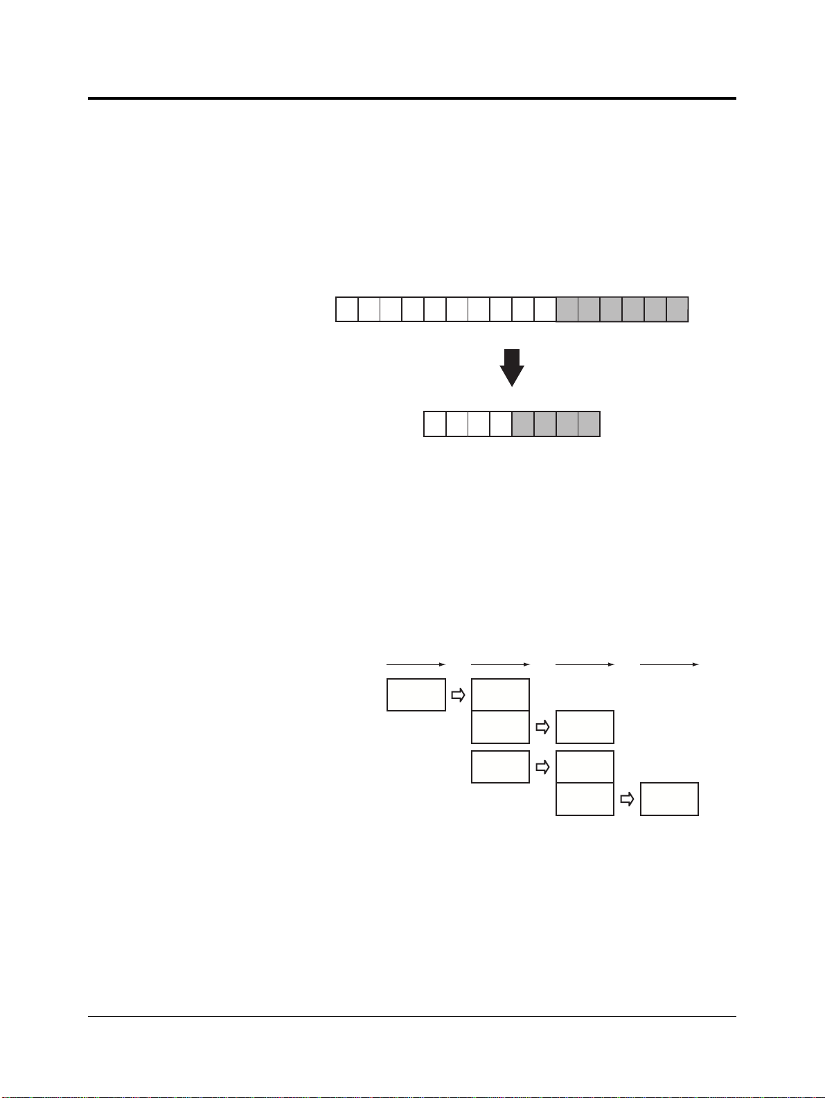
General Description
MN102H Series Features
■ Single-byte basic instruction length
The MN102H series has replaced general registers with eight internal CPU
registers divided functionally into four address registers (A0 - A3) and four
data registers (D0 - D3). The program can address a register pair in four or
less bits, and basic instructions such as register-to-register operations and
load/store operations occupy only one byte.
Conventional code assignment for general register instructions
1514131211109876543210
Register specification
(GRn)
76543210
Register specification
(An/Dn)
New Panasonic code assignments
Figure 1-1 Conventional vs. MN102H Series Code Assignments
■ High-speed pipeline throughput
The MN102H series executes instructions in a high-speed three-stage
pipeline: fetch, decode, execute. With this architecture, the MN102H series
can execute single-byte instructions in only one machine cycle (50 ns at 40
MHz).
1 machine cycle
Instruction 1 Fetch Decode
Instruction 2
Address
calculation
Fetch
Execute
Decode
Address
calculation
Execute
Figure 1-2 Three-Stage Pipeline
■ Simple instruction set
The MN102H series uses a streamlined set of 41 instructions, designed specifically for the programming model for embedded applications. To shrink
code size, instructions have a variable length of one to seven bytes, and the
most frequently used basic instructions are single-byte.
Time
MN102H75K/F75K/85K/F85K LSI User Manual Panasonic Semiconductor Development Company
19
Panasonic
Page 21
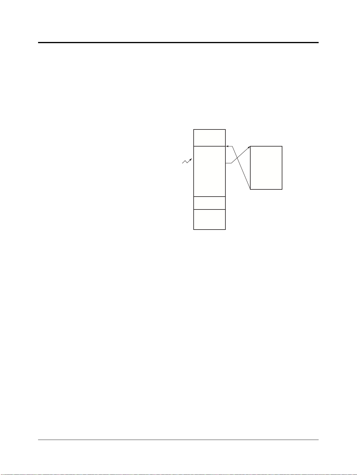
General Description
MN102H Series Features
■ Fast interrupt response
MN102H series devices can stop executing instructions, even those with
long execution cycles, to service interrupts immediately. After an interrupt
occurs, the program branches to the interrupt service routine within six
cycles or less. The architecture also includes a programmable interrupt
handler, which allows you to adjust interrupt servicing speed within the
software when necessary, improving real-time control performance.
Main Program
Instruction 1
Interrupt Service Routine
Instruction 2
Interrupt Request
Instruction 3
Instruction 4
Figure 1-3 MN102H Series Interr upt Servicing
■ Flexible interrupt control structure
The interrupt controller supports a maximum of 64 interrupt vectors.
(Vectors 0 to 3 are nonmaskable interrupt s .) Gr oup s of up to four vectors ar e
assigned to classes, and each class can be set to one of seven priority levels.
This gives the software designer great flexibility and fine control. The core is
also backwards compatible with software from previous Panasonic
peripheral mo dules.
■ High-speed, high-functionality external interface
The MN102H series pro v id es DMA, handshaking, bus arbitration, and other
functions that ensure a fast, efficient interface with other devices.
■ Optimal C-Language development environment
The MN102H series combines hardware optimized for C language programming with a highly efficient C compiler, resulting in assembly codes the
same size as that produced directly in assembly language. This gives
designers the advantage of short development time in a C language environment without the trade-off in code size expansion. The PanaXSeries
development tools support MN102H series devices.
Panasonic Semiconductor Development Company MN102H75K/F75K/85K/F85K LSI User Manual
20
Panasonic
Page 22

General Description
MN102H Series Description
■ Outstanding power savings
The MN102H series contains separate buses for instructions, data, and
peripheral functions, which distributes and reduces load capacitance, dramatically reducing overall power consumption. The series also supports
three HALT and STOP modes for even greater power savings.
The MN102H series is the flagship product for Panasonic’s new high-performance architecture. Panasonic will expand the series as it strives to improve
the CPU core’s performance and speed, and as it develops devices incorporating
ASSPs, ASICs, internal EPROM, and other products to meet the needs of a wide
array of embedded designs.
1.3 MN102H Ser ies Description
This section describes the basic architecture and functions of MN102H series
devices.
■
Processor status word (PSW)
The PSW contains the operation status flags and interrupt mask lev els flags. Note
that the PSW for the MN102H series contains flags for both 16- and 24-bit
operation results.
Bit:1514131211109876543210
—STS1S0IEIM2 IM1 IM 0 VX CX NX ZX VF CF NF ZF
Flags for All 24 Bits Flags for Low-Order 16 Bits
Reset:— 000000000000000
ST: Saturation
This bit controls whether or not the CPU calculates a saturation limit for an
operation. When it is set to 1, the CPU executes a saturate ope ration, and
when it is 0, the CPU executes a normal operation. The PXST instruction
can reverse the meaning of this bit for the next (and only the next) instruction.
S[1:0]: Software control
These bits are the control field for OS software. It is reserved for the OS.
IE: Interrupt enable
If set, this flag enables maskable interrupts; if reset, it disables them.
IM[2:0]: Interrupt mask level
This field indicates the mask level (from 0 to 7) of interrupts that the CPU
will accept from its seven interrupt input pins. The CPU will not accept
any interrupt from a pin at a higher level than that indicated here.
VX: Extension overflow
If the operation causes the sign bit to change in a 24-bit signed number,
this flag is set; otherwise it is reset.
CX: Extension carry flag
If the operation resulted in a carry into (from addition) or a borrow out of
(from subtraction or a comparison) the most significant bit, this flag is set;
otherwise it is reset.
MN102H75K/F75K/85K/F85K LSI User Manual Panasonic Semiconductor Development Company
21
Panasonic
Page 23

General Description
MN102H Series Desc ription
NX: Extension negative flag
If the most significant bit of the result of an operation has the value 1, this
flag is set; if that bit is 0, this flag is reset.
ZX: Extension zero flag
If all bits of the result of an operation have the value 0, this flag is set; otherwise it is reset.
VF: Overflow flag
If the operation causes the sign bit to change in a 16-bit signed number,
this flag is set; otherwise it is reset.
CF: Carry flag
If the operation resulted in a carry into (from addition) or a borrow out of
(from subtraction or a comparison) bit 15, this flag is set; otherwise it is
reset.
NF: Negative flag
If bit 15 of the result of an operation has the value 1, this flag is set; if that
bit is 0, this flag is reset.
ZF: Zero flag
If the least significant 16 bits of the result of an operation have the value 0,
this flag is set; otherwise it is reset.
Panasonic Semiconductor Development Company MN102H75K/F75K/85K/F85K LSI User Manual
22
Panasonic
Page 24
General Description
MN102H Series Description
Program Counter
Address Registers
Data Registers
■ Internal registers, memory, and special function registers
023
PC
A0
A1
A2
A3
D0
D1
D2
D3
The program counter specifies the 24-bit address of the
program instruction being executed.
023
The four address registers specify the location of the data in
the memory. A3 is assigned as the stack pointer.
023
The four data registers handle all arithmetic and logic
operations. When byte-length (8-bit) or word-length (16-bit)
data is to be transferred to memory or to another register, an
instruction adds a zero or sign extension.
Multiplication/Division Register
MDR
Processor Status Word
PSW
Memory, SFRs, and I/O Ports
ROM
RAM
CPUM, EFCR, IAGR
NMICR, xxICR
SCCTRn, TRXBUFn, SCSTRn
ANCTR, ANnBUF
TMn, BCn, BRn, ...
MEMMD
PnOUT, PnIN, PnDIR
015
The dedicated multiplication/division register stores the highorder 16 bits of the 32-bit product of multiplication operations.
In division operations, before execution it stores the high-order
16 bits of the 32-bit dividend, and after execution it stores the
015
16-bit remainder of the quotient.
Memory (ROM and RAM), special function registers for
controlling peripheral functions, and I/O ports can all be
assigned to the same address space.
Internal control registers
Interrupt control registers
Serial interface registers
A/D converter registers
Timer/counter registers
Memory control registers
I/O port registers
1
1
1
1
1
1
1
Note: 1. This a llocation is a representative example. Actual memory, peripheral, SFR, and I/O port configuration depends
on the product.
Figure 1-4 Internal Registers, Memory, and Special Function Registers
MN102H75K/F75K/85K/F85K LSI User Manual Panasonic Semiconductor Development Company
23
Panasonic
Page 25
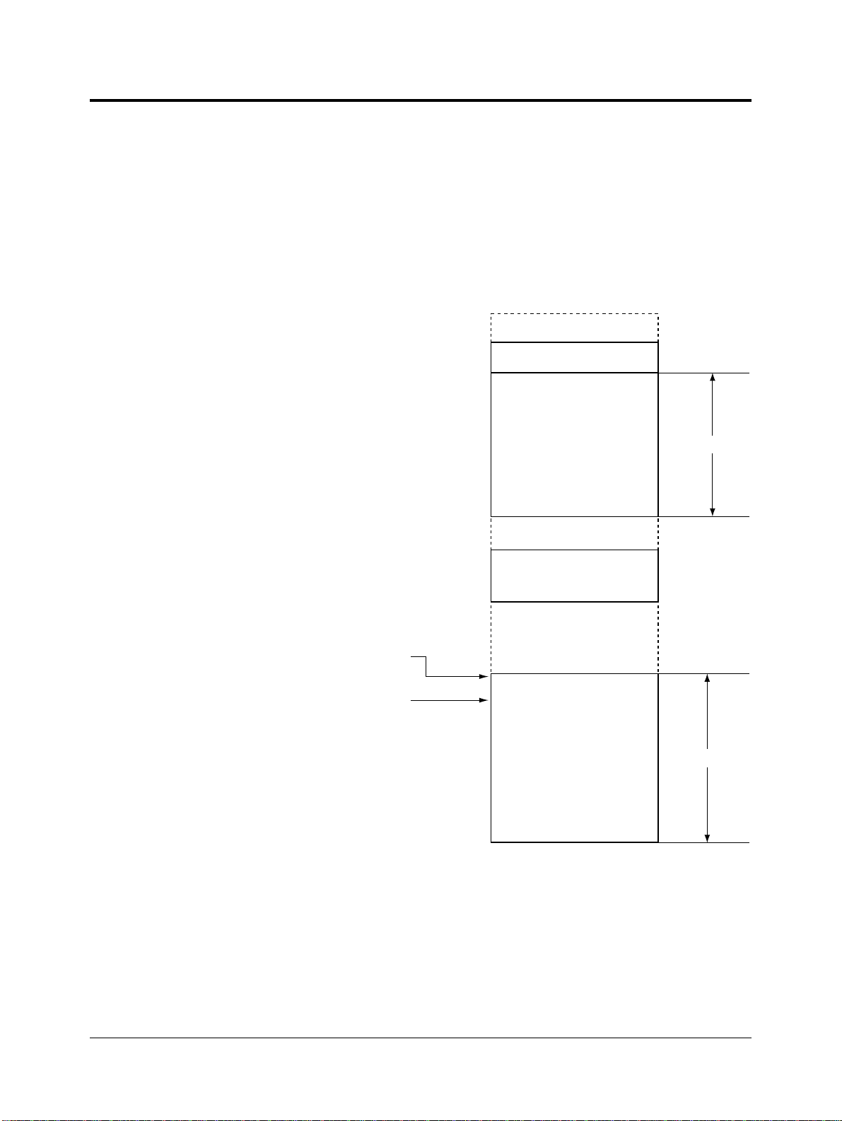
General Description
MN102H Series Desc ription
■ Address space
The memory in the MN102H series is configured as linear address space. The
instruction and data areas are not separated, so the basic segments are internal
ROM, internal RAM, and special function registers.
Figure 1-5 shows the address space for the MN102H75K/85K.The internal ROM
contains the instructions and the font data for the on-screen display (OSD), in any
location. The internal RAM contains the MCU data and the VRAM for the OSD,
in any location.
Program start address
= x’080000’
Interrupt handler start
address = x’080000’
x’007E00’
x’007FFF’
x’008000’
x’009FFF’
x’00FC00’
x’00FFFF’
x’080000’
Special Function
Registers
Internal RAM
Data
OSD
Text VRAM
Graphics VRAM
Special Function
Registers
Internal ROM
Program
OSD
Text fonts
Graphic tiles
8 KB
256 KB
x’0BFFFF’
Figure 1-5 Address Space
Note: In writing, do not use MOVB instruction to access Special Function Registers (x’00FC00’ - x’00FFFF’), access by
word. In reading, access by byte is possible.
Panasonic Semiconductor Development Company MN102H75K/F75K/85K/F85K LSI User Manual
24
Panasonic
Page 26
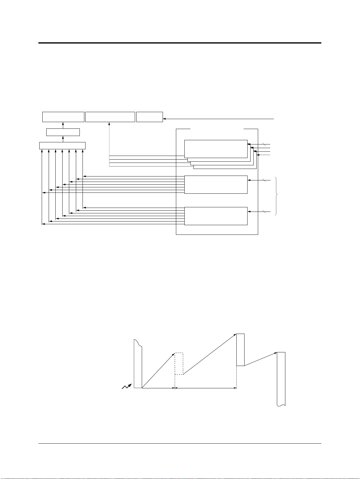
General Description
MN102H Series Description
CPU Core
Maskable Interrupt
Receive
Nonmaskable Interrupt
Receive
■ Interrupt controller
An interrupt controller external to the core controls all nonmaskable and
maskable interrupts except reset. There are a maximum of sixteen interrupt
classes (class 0 to 15). Each class can have up to four interrupt factors and any o f
seven priority levels.
Reset
Receive
Reset
Interrupt Enable
Interrupt Masking
0123456
Nonmaskable Interrupt Controllers
Maskable Interrupt Controllers
Maskable Interrupt Controllers
Note: Interrupt control hardware configuration varies between products.
Figure 1-6 Interrupt Controller Configuration
The CPU checks the processor status word to determine whether or not to accept
an interrupt request. If it accepts the request, automatic hardware servicing
begins and the contents of the program counter and other necessary registers are
pushed to the stack. The program then looks up and branches to th e entry addr ess
of the interrupt service routine for the interrupt that occurred.
Interrupt Controller
Groups 0-3
Nonmaskable Interrupt
Control Registers (NMICR)
Group 4
Maskable Interrupt
Control Registers (xx ICR)
Group 63
Maskable Interrupt
Control Registers (xx ICR)
(WDICR)
(UNICR)
(EIICR)
Nonmaskable interrupts
4
External NMI pin input
Watchdog timer
Undefined instruction
Interrupt occurred,
(
but no vector exists
4
Maskable interrupts
Max. 240 vectors
4
External pin interrupts
()
Peripheral interupts
)
Interrupt preprocessing
Push registers, branch to entry address, etc.
Interrupt
Main program
Max. 6 machine cycles
Hardware processing
Push PC, PSW
7 machine cycles
x'080008'
Interrupt service routine
Header resets interrupt vector
JMP, etc.
Figure 1-7 Interrupt Servicing Se quence
MN102H75K/F75K/85K/F85K LSI User Manual Panasonic Semiconductor Development Company
25
Panasonic
Page 27
General Description
General Specifications
1.4 General Specifications
Table 1-1 General Specifications
Parameter Specification
Structure Internal multiplier (16-bit × 16-bit = 32-bit) and saturate calculator
Load/store architecture
Eight registers:
♦ Four 24-bit data registers
♦ Four 24-bit address registers
Other:
♦ 24-bit program counter
♦ 16-bit processor status word
♦ 16-bit multiply/divide register
Instruction set ♦ 41 instructions
♦ 6 addressing modes
♦ 1-byte basic instruction length
♦ Code assignment: 1 byte (basic) + 0 to 6 bytes (extension)
Performance 12-MHz internal operating frequency (with a 4-MHz external oscilla-
tor)
Instruction execution clock cycles:
♦ Minimum 1 clock cycle (83.3 ns) for register-to-register operations
♦ Minimum 1 clock cycle (83.3 ns) for load/store operations
♦ Minimum 2 clock cycles (167 ns) for branch operations
Pipeline 3-stage: fetch, decode, e xecute
Address space ♦ Linear address space
♦ Shared instruction/data space
Interrupts ♦ 6 external
♦ 30 internal
♦ 7 priority level settings
Low-power modes ♦ STOP
♦ HALT
♦ SLOW
Oscillation frequency
4 MHz (48 MHz with internal PLL)
Panasonic Semiconductor Development Company MN102H75K/F75K/85K/F85K LSI User Manual
26
Panasonic
Page 28
General Description
General Specifications
Table 1-1 General Specifications
Parameter Specification
Timer/counters Four 8-bit timers:
♦ Cascading function (forming 16- or 32-bit timers)
♦ Timer output
♦ Selectable clock source (internal or external)
♦ Serial interface clock generation
♦ Start timing generation for analog-to-digital converter
Two 16-bit timers:
♦ Compare/capture registers
♦ Selectable clock source (internal or external)
♦ PWM and one-shot pulse output
♦ Two-phase encoder input (4x or 1x formats)
16-bit watchdog timer
ROM correction 16 bytes (8-bit × 16)
14
SYSCLK output SY SCLK or SYSC LK/2
Serial interfaces ♦ Two UART/synchronous serial/I
Analog-to-digital
converter
IR remote signal
receiver
PWM 8-bit with 7 channels (3.3-volt tolerance)
Closed-caption
decoder
On-screen display Three-layer format
I/O ports 66(MN102H75K/F75K) / 50(MN102H85K/F85K)
Package 84-pin-QFP(MN102H75K/F75K) / 64-pin-SDIL(MN102H85K/F85K)
2
♦ One I
♦ 8-bit with 12 channels
♦ Automatic scanning
♦ Automatic HEAMA / 5-/6-bit detection
♦ 1-bit interrupt
♦ 2 channels
♦ Internal sync separator
♦ Text layer: 16 × 18 pixels (16 × 26 in closed caption mode), blink-
♦ Graphics layer: 16 × 16 / 16 × 18 pixels
♦ Cursor layer: 16 × 16 / 32 × 32 pixels (1 cursor, displaying one
Color depth: One 16-color palette out of 4096 colors
Dot clock
♦ Internal PLL frequencies: 12, 16, 24, 32 and 48 MHz
♦ External clock: 16–48 MHz
♦ LC blocking oscillator: 16–48 MHz
C interface (multimaster; 2-channel with 1 internal circuit)
ing, outlining, shadowing (f oreground and bac kground), shut ter
effect, italics (CC mode), underlining (CC mode)
graphic tile)
(732.42 Hz)
2
C (master only) interfaces
MN102H75K/F75K/85K/F85K LSI User Manual Panasonic Semiconductor Development Company
27
Panasonic
Page 29
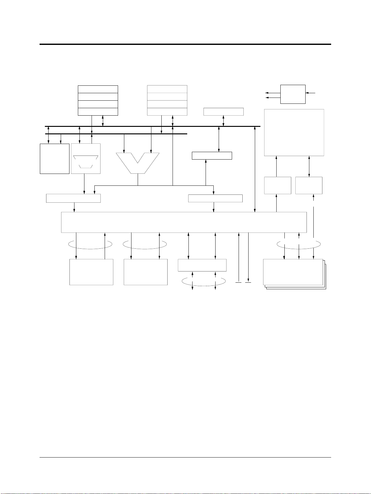
1.5 Block Diagram
Address registers Data registers
A0
A1
A2
A3
D0
D1
D2
D3
Multiplication/Division Register
MDR
General Description
Block Diagram
T1
T2
Clock
generator
Clock
source
A
B
Multiplier
Program address
Program
Counter
Incrementer
ROM bus
PSW
ALU
Operand address
Bus controller
RAM bus
External interface
Internal RAMInternal ROM
External extension bus
Figure 1-8 Functional Block Diagram
BR
BG
Instruction execution
controller
Instruction decoder
Quick decoder
Instruction
queue
Peripherals extension bus
Internal peripheral
Interrupt
controller
Interrupt bus
functions
Panasonic Semiconductor Development Company MN102H75K/F75K/85K/F85K LSI User Manual
28
Panasonic
Page 30

General Description
Block Diagram
Table 1-2 Block Diagram Explanation
Block Description
Clock generator An oscillation circuit connected to an external crystal supplies the
clock to all blocks within the CPU.
Program counter The program counter generates addresses for queued instruc-
tions. Normally it increments based on the sequencer indications,
but for branch instructions it is set as the branch head address,
and for interrupt servicing, it is set as the result of the ALU opera-
tion.
Instruction queue This block contains up to four bytes of prefetched instructions.
Instruction decoder The instruction decoder decodes the contents of the instruction
queue, generates, in the proper sequence, the control signals nec-
essary for executing the instruction, and controls ev ery block in the
chip to execute the instruction.
Quick decoder This block decodes instructions that are 2 bytes or larger in at a
much faster rate than previously possible.
Instruction execution
controller
ALU Arithmetic and logic unit. This block calculates the operand
Multiplier This block multiplies 16 bits × 16 bits = 32 bits.
Internal ROM and
RAM
Address registers
(An)
Operation registers
(Dn, MDR)
PSW The processor status word contains flags that indicate the status
Interrupt controller This block detects interrupt requests from peripheral function
Bus controller This bloc k controls the connection between the CPU’s internal and
Internal peripheral
functions
This block controls the operation of every block within the CPU
using the results from the instruction decoder and interrupt
requests.
addresses for arithmetic operations, logic operations, shift opera-
tions, relative indirect register addressing, indexed addressing,
and indirect register addressing.
These memory blocks contain the program, data, and stack areas.
The address registers store the addresses in memory to be
accessed in data transfers. In relative indirect, indexed, and indi-
rect addressing modes, they store the base address.
The data registers store data to be transferred to memory and
results of operations. In indexed and indirect addressing modes,
they store the offset address.
The multiplication/division register stores data for multiplication
and division operations.
of the CPU interrupt controller and provide information about oper-
ation results.
blocks and requests the CPU to service the interrupt.
external buses. It also contains a bus arbitration function.
MN102H series devices contain a wide range of internal periph-
eral devices, such as timers, serial interfaces, ADCs, and D ACs.
MN102H75K/F75K/85K/F85K LSI User Manual Panasonic Semiconductor Development Company
29
Panasonic
Page 31

1.6 Pin Descriptions
1.6.1 MN102H85K Pin Description
General Description
Pin Descriptions
P00, RMIN, IRQ0
* P01, SDA1
* P02, SCL1
P03, ADIN0
P04, ADIN1
P05, ADIN2
P06, ADIN3
P07, ADIN4
P10, ADIN5, IRQ1
P11, ADIN6, IRQ2
P12, ADIN7, IRQ3
P13, ADIN8, WDOUT
P14, ADIN9, STOP
P15, ADIN10, PWM0
P16, ADIN11, PWM1
P17, PWM2
P20, PWM3
P21, PWM4
P22, PWM5
P23, PWM6
P24, TM4IC, SBT1
P25, TM4IOB, SBI1, SBD1
P26, TM4IOA, SBO1
P27, TM0IO
VDD (VPP)
P30, CLH
VREFHS
P31, CVBS0
VSS
P32, CVBS1
VREFLS
P33, CLL
1
2
3
4
5
6
7
8
9
10
11
12
13
14
15
16
17
18
19
20
21
22
23
24
25
26
27
28
29
30
31
32
64-Pin SDIP
Top Vie w
64
63
62
61
60
59
58
57
56
55
54
53
52
51
50
49
48
47
46
45
44
43
42
41
40
39
38
37
36
35
34
33
VSS
OSC2
OSC1
VDD
P61, SCL0 *
P60, SDA0 *
P57, SBT0
P56, SBI0, SBD0
P55, SBO0
P54, IRQ5, VSYNC
P53, RST
P52, IRQ4, VI0
TEST
P51, YS
P50, SYSCLK
P47, HSYNC
P46, OSDXI
P45, OSDXO
P44, TM5IC, HI1 *
P43, TM5IOB, HI0 *
P42, TM5IOA *
P41, TM1IO *
VCOI
PDO
P40, DAYMOUT, YM
P37, DABOUT, B
P36, DAGOUT, G
P35, DAROUT, R
VREF, P34
IREF
COMP
AVDD
Notes: 1. Pins marked with an asterisk (*) are N-chann el , open-drain pins.
2. Pin 25 is V
in the MN102H85K and VPP in the MN102HF85K.
DD
Figure 1-9 MN102H85K Pin Configuration in Single-Chip Mode
Panasonic Semiconductor Development Company MN102H75K/F75K/85K/F85K LSI User Manual
30
Panasonic
Page 32

General Description
Pin Descriptions
1.6.2 MN102H75K Pin Description
P55, SBO0
P54, IRQ5, VSYNC
P84
NC
P53, RST
P52, IRQ4, VI0
TEST
P51, YS
P83
P50, SYSCLK
P82
P47, HSYNC
P81
P46, OSDXI
P45, OSDXO
* P44, TM5IC, HI1
* P43, TM5IOB, HI0
* P42, TM5IOA
* P41, TM1IO
VCOI
PDO
P85NCP56, SBI0, SBD0
848382818079787776757473727170696867666564
1
2
3
4
5
6
7
8
9
10
11
12
13
14
15
16
17
18
19
20
21
222324252627282930313233343536373839404142
P57, SBT0
P60, SDA0 *
P86
P61, SCL0 *
VDD
OSC1
84-Pin QFP
Top Vie w
OSC2
VSS
P87
P00, RMIN, IRQ0
P01, SDA1 *
P02, SCL1 *
P03, ADIN0
P04, ADIN1
P05, ADIN2
P06, ADIN3
P07, ADIN4
P70
63
62
61
60
59
58
57
56
55
54
53
52
51
50
49
48
47
46
45
44
43
NC
P71
P10, ADIN5, IRQ1
P11, ADIN6, IRQ2
P12, ADIN7, IRQ3
P72
P13, ADIN8, WDOUT
P14, ADIN9, STOP
P73
P15, ADIN10, PWM0
P16, ADIN11, PWM1
P17, PWM2
P20, PWM3
P21, PWM4
P22, PWM5
P23, PWM6
P24, TM4IC, SBT1
P25, TM4IOB, SBI1, SBD1
P26, TM4IOA, SBO1
P27, TM0IO
P74
VREFLS
P32, CVBS1
NC
VSS
P31, CVBS0
VREFHS
P30, CLH
P75
VDD (VPP)
P80
P40, DAYMOUT, YM
P77
P37, DABOUT, B
P36, DAGOUT, G
P76
IREF
AVDD
COMP
VREF, P34
P35, DAROUT, R
P33, CLL
Notes: 1. Pins marked with an asterisk (*) are N-channel, open-drain pins.
2. Pin 41 is V
in the MN102H75K and VPP in the MN102HF75K.
DD
Figure 1-10 MN102H75K Pin Configuration in Single-Chip Mode
MN102H75K/F75K/85K/F85K LSI User Manual Panasonic Semiconductor Development Company
31
Panasonic
Page 33

Table 1-3 Pin Functions
Block Pin Name I/O Pin Count Description
V
DD
V
SS
Power
AV
V
DD/VPP
DD
SYSCLK O 1 System clock output
OSC1 I 1 Oscillator input connection (with internal PLL)
Clocks
OSC2 O 1 Oscillator output connection (with internal PLL)
OSDXI I 1 OSD oscillator input connection (alt. function: P46)
OSDXO O 1 OSD oscillator output connection (alt. function: P45)
Reset RST
Interrupts (external) IRQ0–IRQ5 I6
HSYNC
OSD
VSYNC
YS O 1 Video signal cut
TMnIOA (n=4,5) I /O 2 Input capture/output compare A
16-bit (2)
TMnIOB (n=4,5) I/O 2 Input capture/output compare B
Timers
TMnIC (n=4,5) I 2 Timer/counter clear signal
8-bit (4) TMnIO (n=0,1) I/O 2 Timer clock input/timer output
SBI0/SBI1 I 2 Serial data input
Serial interfaces (2)
SBD0/SBD1 I/O 2 Serial data input
SBO0/SBO1 I/O 2 Serial data output
SBT0/SBT1 I/O 2 Serial clock signal
2
I
C interfaces (2)
SDA0/SDA1 I/O 2 I2C data
SCL0/SCL1 I/O 2 I
IR remote signal receiver RMIN I 1 Remote signal input
PWM (8-bit, 7-channel) PWM0–PWM6 O 7 Pulse width modulator output
I 1 Voltage supply
I 2 Ground reference
I 1 Analog voltage supply
I1
Voltage supply: V
EEPROM version
I/O 1 Reset
(alt. function: P53)
in mask ROM version and VPP in
DD
External interrupt request to microcontroller (alt. functions:
P00, P10, P11, P12, P52, P54)
I 1 Horizontal sync signal input
I 1 Vertical sync signal input
2
C clock
General Description
Pin Descriptions
Panasonic Semiconductor Development Company MN102H75K/F75K/85K/F85K LSI User Manual
32
Panasonic
Page 34

General Description
Pin Descriptions
Table 1-3 Pin Functions (Continued)
Block Pin Name I/O Pin Count Description
P00 –P07 I/O 8 General-purpose port 0 I/O
I/O ports
MN102H75K/HF75K:
total 66 pins
MN102H85K/HF85K:
total 50 pins
I/O ports only in
MN102H75K/F75K
Closed-caption decoders (2)
A/D converter (12-channel) ADIN0–ADIN11 I 12 Analog signal input
D/A converter
(4-bit, 4-channel)
PLL
Mode
Test TEST
Notes: 1. When DAROUT, DAGOUT, DABOUT, and DAYMOUT are used for digital output, their names are R, G, B, and
YM, respectively.
P10 –P17 I/O 8 General-purpose port 1 I/O
P20 –P27 I/O 8 General-purpose port 2 I/O
P30 –P37 I/O 8 General-purpose port 3 I/O
P40 –P47 I/O 8 General-purpose port 4 I/O
P50 –P57 I/O 8 General-purpose port 5 I/O
P60 –P61 I/O 2 General-purpose port 6 I/O
P70 –P77 I/O 8 General-purpose port 7 I/O
P80 –P87 I/O 8 General-purpose port 8 I/O
CVBS0/CBVS1 I 2 Composite video signal input
CLH I 1 Clamp level high input
CLL I 1 Clamp level low input
VREFHS I 1 CCD reference voltage input
VREFLS I 1 CCD reference voltage input
DAROUT
DAGOUT
DABOUT
DAYMOUT
(1)
(1)
(1)
(1)
IREF I 1 Resistance connection for DAC bias current setting
VREF I 1 DAC reference voltage connection
COMP I 1 DAC phase compensator connection
VCOI I 1 Internal VCO input (external LPF input)
PDO O 1 Internal phase compare output (external LPF output)
STOP O 1 STOP mode status signal
WDOUT O 1 Watchdog timer overflow signal
O 1 DAC output (red)
O 1 DAC output (green)
O 1 DAC output (blue)
O 1 DAC output (YM)
I 1 Test pin (Connect to ground.)
MN102H75K/F75K/85K/F85K LSI User Manual Panasonic Semiconductor Development Company
33
Panasonic
Page 35

General Description
W
Pin Descriptions
■ Considerations for power supply, clock, and reset pins
DD
V
V
DD
Power
Supply
V
SS
MN102H75K
MN102H85K
V
SS
Note: If the circuit uses the same po we r sup ply fo r di gita l a n d an al og sup pli es, co nn ect
the pins in the location closest to the power supply.
Figure 1-11 Power Supply Wiring
AV
AV
DD
SS
OSC1
4 MHz
OSC2
0.1 µF
4 MHz
Note: The capacitance values vary depending on the oscillator.
Figure 1-12 OSC1 and OSC2 Connection Examples
10 kΩ - 50 kΩ
RST
10 µF - 100 µF
+
-
Figure 1-13 Reset Pin Connection Example 1
OSDXI
16MHz - 48MHz
OSDXO
OSC1
OSDXI
Oscillation
Circuit
Di
S
OSC2
OSDXO
16MHz - 48MHz
Oscillation
Circuit
Note: The capacitance values vary depending on the oscillator.
Figure 1-14 OSDXI and OSDXO Connection Examples
■ Connection the PLL circuit
The MN102H75K/85K contains an internal PLL circuit. To use this circuit, you
must connect it to an external (lag-lead) filter.
Panasonic Semiconductor Development Company MN102H75K/F75K/85K/F85K LSI User Manual
34
Panasonic
Page 36

General Description
Bus Interface
1.7 Bus Int erface
1.7.1 Description
The bus interface operates in external extension mode. Figure 1-15 provides the
memory space for the MCU in this mode.
External Expansion Mode
Reset start
x'000000'
x'008000'
x'00A000'
x'00FC00'
x'010000'
x'080000'
x'0C0000'
x'200000'
x'400000'
x'800000'
x'C00000'
x'FFFFFF'
External devices
Internal RAM
(8192 bytes
(*4)
Peripheral registers
External devices
Internal masked ROM
(256 Kbytes
(*2)
External devices
Expandable up to 16 MB
(*3)
(*1)
)
External memory space 0 (CS0 signal):
IR remote signal receive
2
C
I
)
OSD
CCD0
CCD1
H counter
PWM
External memory space 1
(CS1 signal)
External memory space 2
(CS2 signal)
External memory space 3
(CS3 signal)
Cannot be accessed.
MN102H75K*1256 Kbytes*2x'0C0000'*38192 bytes*4x'00A000'
Figure 1-15 Memory Space in External Extension Mode
MN102H75K/F75K/85K/F85K LSI User Manual Panasonic Semiconductor Development Company
35
Panasonic
Page 37

General Description
Bus Interface
1.7.2 Bus Interface Control Registers
The external memory wait register (EXWMD) and memory mode register 1
(MEMMD1) control the bus interface.
EXWMD: External Memory Wait Register x’00FF80’
Bit:1514131211109876543210
EW 33 EW 32 EW 31 EW 30 E W 23 EW 22 EW 21 EW 20 EW 13 EW 12 EW 11 EW 10 EW 03 EW 02 EW 01 EW 00
Reset:1110111011101110
R/W: R/WR/WR/WR/WR/WR/WR/WR/WR/WR/WR/WR/WR/WR/WR/WR/W
EW[33:30], EW[23:20], EW[13:10], EW[03:00]
These fields contain the wait settings for external memory spaces 3, 2, 1,
and 0, respectively. One wait corresponds to one instruction cycle. When
the external oscillator is 4 MHz, one wait is 83 ns.
The OSD, VBI0, VBI1, I2C, IR remote signal receiver, and H counter
blocks apply to external memory space 0.
Table 1-4 Wait Count Settings
EW[n3:n0] Setting Wait Count Cycles
0000 0.01.0
0001 R es e rved
0010 1.02.0
0011 Res erved
0100 2.03.0
0101 R es e rved
0110 3.04.0
011 1 Res e rved
1000 4.05.0
1001 R es e rved
1010 5.06.0
1011 Res erved
1100 6.07.0
1101 R eser ved
1110 7. 08.0
1111 R eser ve d
MEMMD1: Memory Mode Register 1 x’00FF82’
Bit:1514131211109876543210
EB31 EB32 EB21 EB20 EB11 EB10 EB01 EB00 BRS1 BRS0 BRC3 BRC2 BRC1 BRC0 IOW 1 IOW 0
Reset:0000000000000011
R/W: R/WR/WR/WR/WR/WR/WR/WR/WR/WR/WR/WR/WR/WR/WR/WR/W
Write 0s to bits 15 to 2.
IOW[1:0]: Wait setting for internal I/O space
00:1 wait
01:Reserved
10:2 waits
11:3 waits
Panasonic Semiconductor Development Company MN102H75K/F75K/85K/F85K LSI User Manual
36
Panasonic
Page 38

Interrupts
Description
2 Interrupts
2.1 Description
The most important factor in real-time control is an MCU’s speed in servicing
interrupts. The MN102H75K/85K has an extremely fast interrupt response time
due to its ability to abort instructions, such as multiply or divide, that require
multiple clock cycles. The MN102H75K/85K re-executes an aborted instruction
after returning from the interrupt service routine.
This section describes the interrupt system in the MN102H75K/85K. The
MN102H75K/85K contains 36 interru pt group contro llers. Each controls a singl e
interrupt group. Because each group contains only one interrupt vector, the
MN102H75K/85K can handle interrupts much quicker than previously possible.
Each interrupt group belongs to one of twelve classes, which defines its interrupt
priority level.
With the exception of reset interrupts, all interrupts from timers, other peripheral
circuits, and external pins must be registered in an interrupt group controller.
Once they are registered, interrupt requests are sent to the CPU in accordance
with the interrupt mask level (0 to 6) set in the interrupt group controller. Groups
1 to 3 are dedicated to system interrupts. Table 2-1 compares the interrupt
parameters of the MN102H75K/85K to those of the MN102L35G, the comparable MCU in the previous generation of the 16-bit series.
Table 2-1 Comparison of MN102H75K/85K and MN102L35G Interrupt Features
Parameter MN102L35G MN102H75K/85K
Interrupt groups
(IAGR group numbers
Interrupt response time Good Excellent
Interrupt level settings 4 vectors per level 4 vectors per level
Software compatibility — Easily modified
4 vectors per group
(Separated by interrupt
service routine)
1 vector per group
(Group number gener-
ated for each interrupt)
The MN102H75K/85K has six e xter nal int errupt pins. S et th e interru pt con dition
(positive edge, negative edge, either edge, or active low) in the EXTMD register.
Internal
interrupts
.
.
.
IRQ0
IRQ1
IRQ2
IRQ3
IRQ4
IRQ5
.
.
.
EXTMD
Edge/level
Edge/level
Edge/level
Edge/level
Edge/level
Edge/level
Interrupt
to CPU
Interrupt
arbitration
Figure 2-1 Interrupt Controller Block Diagram
MN102H75K/F75K/85K/F85K LSI User Manual Panasonic Semiconductor Development Company
37
Panasonic
Page 39

Interrupts
Description
MN102H
CPU Core
Levels 0 6
Group Interrupt Vector
Group 0
NMIs
Group 1 Watchdog timer
Group 2 Undefined instruction
Group 3 Error interrupt
Group 4 External interrupt 0
Group 5 External interrupt 1
Group 6
Group 7
Group 8 External interrupt 2
Group 9 External interrupt 3
Group 10
Group 11
Group 12 External interrupt 4
Group 13 External interrupt 5
Group 14
Group 15
Group 16 Timer 4 compare/capture B
Group 17 Timer 4 compare/capture A
Group 18 Timer 4 underflow interrupt
Group 19 VBI interrupt (1)
Group 20 Timer 5 compare/capture B
Group 21 Timer 5 compare/capture A
Group 22 Timer 5 underflow interrupt
Group 23 VBI interrupt (2)
Group 24 Timer 2 underflow interrupt
Group 25 Timer 1 underflow interrupt
Group 26 Timer 0 underflow interrupt
Group 27 Remote signal receive int.
Group 28 Address 3 match interrupt
Group 29 Address 2 match interrupt
Group 30 Address 1 match interrupt
Group 31 Address 0 match interrupt
Group 32 A/D conversion end int.
Group 33 Serial 0 transmission end
Group 34 Serial 0 reception end
Group 35
Group 36 VBIVSYNC interrupt (1)
Group 37 VBIVSYNC interrupt (2)
Group 38 Timer 3 underflow interrupt
Group 39
Group 40 OSD interrupt (graphics)
Group 41 OSD interrupt (text)
Group 42
Group 43
Group 44 Serial 1 transmission end
Group 45 Serial 1 reception end
Group 46 I
Group 47
2
C interrupt
Priority
Level
Class
0
Class
1
Class
2
Class
3
Class
4
Class
5
Class
6
Class
7
Class
8
Class
9
Class
10
Class
11
Register
Address
00FC42 (R/W)
00FC44 (R/W)
00FC46 (R/W)
00FC48 (R/W)
00FC4A (R/W)
00FC50 (R/W)
00FC52 (R/W)
00FC58 (R/W)
00FC5A (R/W)
00FC60 (R/W)
00FC62 (R/W)
00FC64 (R/W)
00FC66 (R/W)
00FC68 (R/W)
00FC6A (R/W)
00FC6C (R/W)
00FC6E (R/W)
00FC70 (R/W)
00FC72 (R/W)
00FC74 (R/W)
00FC76 (R/W)
00FC78 (R/W)
00FC7A (R/W)
00FC7C (R/W)
00FC7E (R/W)
00FC80 (R/W)
00FC82 (R/W)
00FC84 (R/W)
00FC88 (R/W)
00FC8A (R/W)
00FC8C (R/W)
00FC90 (R/W)
00FC92 (R/W)
00FC98 (R/W)
00FC9A (R/W)
00FC9C (R/W)
Figure 2-2 Interrupt Vector Group and Class Assignments
Panasonic Semiconductor Development Company MN102H75K/F75K/85K/F85K LSI User Manual
38
Panasonic
Page 40

Interrupts
Description
Program
Interrupt
Max. 6 cycles
Interrupt hardware processing
(9 cycles)
rti (7 cycles)
Address 80008
Handler
(preprocessing)
jsr (5 cycles)
rts (5 cycles)
Handler
(postprocessing)
Registers popped
Interrupt service
routine
The interrupt request is
deleted in the header
(Included in the cycle
count shown to the left.)
Figure 2-3 Interrupt Servicing Time
Table 2-2 Handler Preprocessing
Sequence Assembler Bytes Cycles
Push registers add -8,A3
mov A0,(A3)
movx D0,(4,A3)
Interrupt ACK mov (FC0E),D0 31
Generate header address
for interrupt service routine
mov BASE,A0
mov (D0,A0),A0
Branch jsr (A0) 25
Tota l 17 15
2
2
3
3
2
1
2
3
1
2
Table 2-3 Handler Postprocessing
Sequence Assembler Bytes Cycles
Pop registers mov (A3),A0
movx (4,A3),D0
add 8,A3
Tota l 7 6
2
3
2
2
3
1
MN102H75K/F75K/85K/F85K LSI User Manual Panasonic Semiconductor Development Company
39
Panasonic
Page 41

Interrupts
Interrupt Setup Examples
2.2 Interrupt Setup Examples
2.2.1 Setting Up an External Pin Interrupt
In this example, an interrupt occurs on a falling-edge signal from the IRQ0 (P00)
external interrupt pin, and the interrupt priority level is 5.
On reset, the external edge setting in the EXTMD register is low (b’00’ = activelow interrupt), and the IQ0IR bit of the IQ0ICL register is 0.
IRQ0
P5
P0
P2
CORE
Interrupts
Timers 0-5
ROM, RAM
Bus Controller
Serial I/Fs
P1
P3
ADC
Figure 2-4 Block Diagram of External Pin Interrupt
■
Enabling external interrupt 0
1. Set the interrupt conditions for the IRQ0 (P00) pin. For this example, set the
IQ0TG[1:0] bits of EXTMD to b’10’ (negative-edge-triggered interrupt).
EXTMD (example) x’00FCF8’
Bit: 15 14 13 12
0000
Setting:———— 0 0 0000000010
11 10 9 8
IQ5TG1IQ5TG0IQ4TG1IQ4TG0IQ3TG1IQ3TG0IQ2TG1IQ2TG0IQ1TG1IQ1TG0IQ0TG1IQ0TG
76543210
0
2. Cancel any existing interrupt requests and enable IRQ0 interrupts. To do
this, set the IQ0IR bit of IQ0ICL to 0, set the IQ0LV[2:0] bits of IQ0ICH to
b’101’ (priority level 5), and set the IQ0IE bit to 1.
IQ0ICL (example) x’00FC48’
Bit:76543210
— — — IQ0IR — — — IQ0ID
Setting:00000000
IQ0ICH (examp le) x’00FC49’
Bit:76543210
— IQ0LV2 IQ0LV1 IQ0LV0 — — — IQ0IE
Setting:01010001
Panasonic Semiconductor Development Company MN102H75K/F75K/85K/F85K LSI User Manual
40
Panasonic
Page 42

Interrupts
Interrupt Setup Examples
The main program normally generates and branches to the interrupt start address.
3. Enable interrupts by writing a 1 to the interrupt enable flag (IE) in the PSW
and setting the interrupt masking level (IM[2:0]) to 7 (b’111’).
Now if a falling edge occurs on IRQ0 (P00), an interrupt will occur. If the
CPU accepts the interrupt, the program branches to address x’080008’.
Servicing the interrupt
■
4. During interrupt preprocessing, read the accepted interrupt group number
register (IAGR) to determine the interrupt group (group 4, in this case).
5. Branch to the interrupt service routine.
During the interrupt service routine, prevent the CPU from
accepting any other maskable
interrupts by setting the IM[2:0]
and IE bits of the PSW to 0.
To acce pt the same interrupt
during the interrupt service routine, clear IR flag at the beginning of it.
6. At the beginning of the interrupt service routine, clear the IQ0IR bit in
IQ0ICL to 0.
7. After the service routine ends, return to the main program with the RTI
instruction.
P00 (IRQ0)
EXTMD
IQ0IE
IQ0IR
Interrupt servicing
Registers [R/W]
Sequence
Figure 2-5 Timing for External Pin Interrupt Setup (Example)
Low level
Falling edge
EXTMD(W) IQ0ICL(B)
IQ0ICL(B)
(1) (2)(3) (4)(5)(6)(7)
IQ0ICL(B)IQ0ICH(B)
(4)(5)(6)(7)
MN102H75K/F75K/85K/F85K LSI User Manual Panasonic Semiconductor Development Company
41
Panasonic
Page 43

The watchdog timer interr upt is
provided for detecting and handling
racing. Normal operati on i s not
guaranteed if the progr am returns
after a watchdog in terrupt. For
actions requiring retu rns, us e a
timer interrupt.
Interrupts
Interrupt Setup Examples
2.2.2 Setting Up a Watchdog Timer Interrupt
In this example, a watchdog timer reset occurs. The watchdog timer starts
running after a reset, when the NWDEN flag in the CPU mode register (CPUM)
is enabled (set to 0). When the watchdog timer overflows, a nonmaskable
interrupt occurs. This means that the w atchdo g timer must b e cleared in the main
program.
P0
P5
CORE
Interrupts
ROM, RAM
Bus Controller
P1
P3
If WDM[1:0] = 00, a watchdog
interrupt occurs when the watchdog timer counts 2
(5.4613 ms at 4-MHz f
MHz f
SYSCLK
tings have the following meanings:
The main program normally
clears the watchdog timer prior
to a watchdog interrupt.
00: 2
01: 2
10: 2
11: 2
16
4
12
14
16
cycles
). The WDM set-
(5.46 ms)
(1.33 µs)
(0.34 ms)
(1.37 ms)
OSC
/12-
P2
Timers 0-5
Serial I/Fs
ADC
Figure 2-6 Block Diagram of Watchdog Timer Interrupt
Enabling watchdog timer interrupts
■
1. Enable interrupts by writing a 1 to the interrupt enable flag (IE) in the PSW
and setting the interrupt masking level (IM[2:0]) to 7 (b’111’).
2. Activate the wa tchdo g ti mer by clearing t he NWDEN bit o f th e CPUM re gi ster. Set the time limit for the racing detection function in the WDM[1:0 ]
field.
CPUM (example) x’00FC00’
Bit:1514131211109876543210
NW
WDM1WDM
DEN
Setting:0000000000000000
————————
0
OSC
STOP HAL T OSC1 OSC0
ID
■ Clearing the watchdog timer
3. Set the NWDEN bit in CPUM to 1, then immediately reset it to 0. The
watchdog timer clears to 0 when NWDEN is 1.
Panasonic Semiconductor Development Company MN102H75K/F75K/85K/F85K LSI User Manual
42
Panasonic
Page 44

Interrupts
Interrupt Setup Examples
The main program normally generates and branches to the interrupt start address.
If the CPU accepts an interrupt, the program branches to address x’080008’.
The oscillator delay timer shares the counter for the watchdog timer. The
oscillator delay timer is activated when the circuit exits the STOP mode, so the
program must clear the WDID flag to 0 prior to entering the STOP mode. It must
also reclear WDID after returning to NORMAL mode. For further details, see
section 2-6, “Standby Function,” in the MN10200 Series Linear Addressing
Version LSI User Manual.
Overflow
RST
WD count
NWDEN (CPUM)
WDID (WDICR)
Interrupt servicing
Registers [R/W]
Sequence
CPUM (W) CPUM (W) CPUM (W)
(1) (2) (3) (2)
Figure 2-7 Timing for Watchdog Timer Interrupt Setup (Example)
Clear
MN102H75K/F75K/85K/F85K LSI User Manual Panasonic Semiconductor Development Company
43
Panasonic
Page 45

Interrupts
Interrupt Control Registers
2.3 Interrupt Control Registers
A control register is assigned to each interrupt vector group. Except for the class
0 registers (WDICR, PIICR, and EIICR), the control registers allow you to
enable and set the priority level for interrupt groups.
Below is the general format of the registers in class 0 and classes 1 to 11.
Class 0 (X):
WD (watchdog overflow interrupts)
PI (undefined instruction interrupts)
EI (interrupt error interrupts)
XICR (System Interrupt)
Bit:76543210
———————ID
ID : Interrupt detect flag
0: Interrupt undetected
1: Interrupt detected
Classes 1–11 (X):
IQ (external interrupts)
TM (timer interrupts)
SC (serial interrupts)
I2C (I2C interrupts)
OSD (OSD interrupts)
AN (A/D conversion end interrupts)
RMC (remote signal receive interrupts)
VBI (VBI interrupts)
ADM (address match interrupts)
XnICH (System Interrupt)
Bit:76543210
— LV2 LV1 LV0 — — — IE
LV[2:0]: Interrupt priority level
Sets the priority from 0 to 6 (000 = 0, 001 = 1, etc.). When LV = 7, interrupts are not serviced.
Note that some registers do not contain the LV field. In this case, these bits
always read 0.
IE: Interrupt enable flag
0: Disable
1: Enable
Panasonic Semiconductor Development Company MN102H75K/F75K/85K/F85K LSI User Manual
44
Panasonic
Page 46

Interrupts
Interrupt Control Registers
XnICL (System Interrupt)
Bit:76543210
———IR———ID
IR: Interrupt request flag
0: No interrupt requested
1: Interrupt requested
ID: Interrupt detect flag
0: Interrupt undetected
1: Interrupt detected
The following is an example program setting an interrupt group’s priority level
(LV field) and enabling the in terrup t group (IE) in the interrupt control register
(XnICH). Note that interrupts must be disabled during this rou tine.
Example 2-1 Setting the Interrupt Priority Level
... ;
and 0xf7ff,psw ;Clear the IE bit of the PSW.
nop ; Inserted to ensure that IE clears
nop ; completely, so XnICH is accessible.
mov d0,(XnICH) ;Write to LV/IE
mov (XnICH),d0 ;Synchronize with the store buffer.
or 0x0800,psw ;Set the IE bit of the PSW.
... ;
The program does not need to clear the IE bit of the PSW to disable interrupts
during interrupt servicing, since the interrupt service routine has already cleared
it.
You can replace the NOP instructions in the example above with any instruction
except for those that modify the PSW IE bit or the LV or IE bits of an XnICH
register. Inserting any of these instructions would cause interrupt error to occur.
The example includes two NOP instructions to ensure that the minimum number
of cycles required for a write to IE have passed. However, you can also insert
more than two NOPs.
Table 2-4 provides a list of the interrupt control registers, and a description of the
fields in each register follows.
MN102H75K/F75K/85K/F85K LSI User Manual Panasonic Semiconductor Development Company
45
Panasonic
Page 47
Interrupt Control Registers
Table 2-4 Interrupt Control Registers
Register Address R/W Description
IAGR x’00FC0E’ R Accepted interrupt group number register
WDICR x’00FC42’ R/W Watchdog interrupt control register
PIICR x’00FC44’ R/W Undefined instruction interrupt control register
EIICR x’00FC46’ R Interrupt error interrupt control register
EXTMD x’00FCF8’ R/W External interrupt mode register
IQ0ICL
IQ0ICH
IQ1ICL
IQ1ICH
IQ2ICL
IQ2ICH
IQ3ICL
IQ3ICH
IQ4ICL
IQ4ICH
IQ5ICL
IQ5ICH
TM4CBICL
TM4CBICH
TM4CAICL
TM4CAICH
TM4UDICL
TM4UDICH
VBIICL
VBIICH
TM5CBICL
TM5CBICH
TM5CAICL
TM5CAICH
TM5UDICL
TM5UDICH
VBIWICL
VBIWICH
TM2UDICL
TM2UDICH
TM1UDICL
TM1UDICH
TM0UDICL
TM0UDICH
RMCICL
RMCICH
x’00FC48’
x’00FC49’
x’00FC4A’
x’00FC4B’
x’00FC50’
x’00FC51’
x’00FC52’
x’00FC53’
x’00FC58’
x’00FC59’
x’00FC5A’
x’00FC5B’
x’00FC60’
x’00FC61’
x’00FC62’
x’00FC63’
x’00FC64’
x’00FC65’
x’00FC66’
x’00FC67’
x’00FC68’
x’00FC69’
x’00FC6A’
x’00FC6B’
x’00FC6C’
x’00FC6D’
x’00FC6E’
x’00FC6F’
x’00FC70’
x’00FC71’
x’00FC72’
x’00FC73’
x’00FC74’
x’00FC75’
x’00FC76’
x’00FC77’
R/W
External interrupt 0 interrupt control register (low)
R/W
External interrupt 0 interrupt control register (high)
R/W
External interrupt 1 interrupt control register (low)
R/W
External interrupt 1 interrupt control register (high)
R/W
External interrupt 2 interrupt control register (low)
R/W
External interrupt 2 interrupt control register (high)
R/W
External interrupt 3 interrupt control register (low)
R/W
External interrupt 3 interrupt control register (high)
R/W
External interrupt 4 interrupt control register (low)
R/W
External interrupt 4 interrupt control register (high)
R/W
External interrupt 5 interrupt control register (low)
R/W
External interrupt 5 interrupt control register (high)
R/W
Timer 4 compare/capture B interrupt control register (low)
R/W
Timer 4 compare/capture B interrupt control register (high)
R/W
Timer 4 compare/capture A interrupt control register (low)
R/W
Timer 4 compare/capture A interrupt control register (high)
R/W
Timer 4 underflow interrupt control register (low)
R/W
Timer 4 underflow interrupt control register (high)
R/W
VBI (1) interrupt control register (low)
R/W
VBI (1) interrupt control register (high)
R/W
Timer 5 compare/capture B interrupt control register (low)
R/W
Timer 5 compare/capture B interrupt control register (high)
R/W
Timer 5 compare/capture A interrupt control register (low)
R/W
Timer 5 compare/capture A interrupt control register (high)
R/W
Timer 5 underflow interrupt control register (low)
R/W
Timer 5 underflow interrupt control register (high)
R/W
VBI (2) interrupt control register (low)
R/W
VBI (2) interrupt control register (high)
R/W
Timer 2 underflow interrupt control register (low)
R/W
Timer 2 underflow interrupt control register (high)
R/W
Timer 1 underflow interrupt control register (low)
R/W
Timer 1 underflow interrupt control register (high)
R/W
Timer 0 underflow interrupt control register (low)
R/W
Timer 0 underflow interrupt control register (high)
R/W
Remote signal receive interrupt control register (low)
R/W
Remote signal receive interrupt control register (high)
Interrupts
Panasonic Semiconductor Development Company MN102H75K/F75K/85K/F85K LSI User Manual
46
Panasonic
Page 48

Interrupts
Interrupt Control Registers
Table 2-4 Interrupt Control Registers
Register Address R/W Description
ADM3ICL
ADM3ICH
ADM2ICL
ADM2ICH
ADM1ICL
ADM1ICH
ADM0ICL
ADM0ICH
ANICL
ANICH
SCT0ICL
SCT0ICH
SCR0ICL
SCR0ICH
VBIVICL
VBIVICH
VBIVWICL
VBIVWICH
TM3UDICL
TM3UDICH
OSDGICL
OSDGICH
OSDCICL
OSDCICH
SCT1ICL
SCT1ICH
SCR1ICL
SCR1ICH
I2CICL
I2CICH
x’00FC78’
x’00FC79’
x’00FC7A’
x’00FC7B’
x’00FC7C’
x’00FC7D’
x’00FC7E’
x’00FC7F’
x’00FC80’
x’00FC81’
x’00FC82’
x’00FC83’
x’00FC84’
x’00FC85’
x’00FC88’
x’00FC89’
x’00FC8A’
x’00FC8B’
x’00FC8C’
x’00FC8D’
x’00FC90’
x’00FC91’
x’00FC92’
x’00FC93’
x’00FC98’
x’00FC99’
x’00FC9A’
x’00FC9B’
x’00FC9C’
x’00FC9D’
R/W
Address 3 match interrupt control register (low)
R/W
Address 3 match interrupt control register (high)
R/W
Address 2 match interrupt control register (low)
R/W
Address 2 match interrupt control register (high)
R/W
Address 1 match interrupt control register (low)
R/W
Address 1 match interrupt control register (high)
R/W
Address 0 match interrupt control register (low)
R/W
Address 0 match interrupt control register (high)
R/W
A/D conversion end interrupt control register (low)
R/W
A/D conversion end interrupt control register (high)
R/W
Serial 0 transmission end interrupt control register (low)
R/W
Serial 0 transmission end interrupt control register (high)
R/W
Serial 0 reception end interrupt control register (low)
R/W
Serial 0 reception end interrupt control register (high)
R/W
VBIVSYNC (1) interrupt control register (low)
R/W
VBIVSYNC (1) interrupt control register (high)
R/W
VBIVSYNC (2) interrupt control register (low)
R/W
VBIVSYNC (2) interrupt control register (high)
R/W
Timer 3 underflow interrupt control register (low)
R/W
Timer 3 underflow interrupt control register (high)
R/W
OSD (graphics) interrupt control register (low)
R/W
OSD (graphics) interrupt control register (high)
R/W
OSD (text) interrupt control register (low)
R/W
OSD (text) interrupt control register (high)
R/W
Serial 1 transmission end interrupt control register (low)
R/W
Serial 1 transmission end interrupt control register (high)
R/W
Serial 1 reception end interrupt control register (low)
R/W
Serial 1 reception end interrupt control register (high)
2
C interrupt control register (low)
R/W
I
2
I
C interrupt control register (high)
R/W
Note: The interrupt error interrupt control register does not exist in the hardware,
but if no matching interrupt vector is found for an interrupt that occurs, the
CPU writes a C to IAGR to indicate that it detected an abnormality.
MN102H75K/F75K/85K/F85K LSI User Manual Panasonic Semiconductor Development Company
47
Panasonic
Page 49

Interrupts
Interrupt Control Registers
IAG R: Accepted Inte rrupt Group Numb er Regis te r x’00FC0E’
Bit:1514131211109876543210
————————GN5GN4GN3GN2GN1GN0——
Reset:0000000000000000
R/W:RRRRRRRRRRRRRRRR
IAGR returns the group number of an accepted interrupt, indicated in the
6-bit GN field. When the interrupt handler has to calculates the header
address for the interrupt service routine, it merely needs to add the contents
of IAGR to the hea der address fo r the table in wh ich are registered the vector addresses for servicing all interrupts. IAGR is a 16-bit access register.
GN[5:0]: Group Number
Contains the group number multiplied by four.
EXTMD: External Interrupt Mode Register x’00FCF8’
Bit:1514131211109876543210
————
Reset:0000000000000000
R/W: R R R R R/W R/W R/W R/W R/W R/W R/W R/W R/W R/W R/W R/W
IQ5TG1IQ5TG0IQ4TG1IQ4TG0IQ3TG1IQ3TG0IQ2TG1IQ2TG0IQ1TG1IQ1TG0IQ0TG1IQ0TG
0
The watchdog timer interr upt is
provided for detecting and handling
racing. Normal operati on i s not
guaranteed if the progr am returns
after a watchdog in terrupt. For
actions requiring retu rns, us e a
timer interrupt.
EXTMD sets the trigger conditions for external interrupts. IQnTG[1:0]
sets the interrupt mode on the associated IRQ pin. Each IRQ pin can have
any polarity or edge setting. EXTMD is a 16-bit access register.
00:Active-low interrupt
01:Either-edge-triggered interrupt (positive or negative)
10:Negative-edge-triggered interrupt
11:Positive-edge-triggered interrupt
WDICR: Watchdog Interrupt Control Register x’00FC42’
Bit:76543210
———————WDID
Reset:00000000
R/W:RRRRRRRR/W
WDICR is an 8-bit access register.
WDID: Watchdog interrupt detect flag
0: Interrupt undetected
1: Interrupt detected
Panasonic Semiconductor Development Company MN102H75K/F75K/85K/F85K LSI User Manual
48
Panasonic
Page 50

Interrupts
Interrupt Control Registers
PIICR: Undefined Instruction Interrupt Control Register x’00FC44’
Bit:76543210
———————PIID
Reset:00000000
R/W:RRRRRRRR/W
PIICR is an 8-bit access register.
PIID: Undefined instruction interrupt detect flag
0: Interrupt undetected
1: Interrupt detected
EIICR: Interrupt error Interrupt Control Register x’00FC46’
Bit:76543210
————————
Reset:00000000
R/W:RRRRRRRR
EIICR does not exist in the hardware, but if the CPU finds no matching
interrupt vector for an interrupt that occurs, it writes a C to IAGR to indicate that it detected an abnormality. EIICR is an 8-bit access register.
IQ0ICL: External Interrupt 0 Interrupt Control Register (Low) x’00FC48’
Bit:76543210
— — — IQ0IR — — — IQ0ID
Reset:00000000
R/W:RRRR/WRRRR
IQ0ICL requests and verifies interrupt requests for external interrupt 0. It
is an 8-bit access register. Use the MOVB instruction to access it.
IQ0IR: External interrupt 0 interrupt request flag
0: No interrupt requested
1: Interrupt requested
IQ0ID: External interrupt 0 interrupt detect flag
0: Interrupt undetected
1: Interrupt detected
MN102H75K/F75K/85K/F85K LSI User Manual Panasonic Semiconductor Development Company
49
Panasonic
Page 51

Interrupts
Interrupt Control Registers
IQ0ICH: External Interrupt 0 Interrupt Control Register (High) x’00FC49’
Bit:76543210
— IQ0LV2 IQ0LV1 IQ0LV0 — — — IQ0IE
Reset:00000000
R/W: R R/W R/W R/W R R R R/W
IQ0ICH sets the priority level for and enables external interrupt 0. It is an
8-bit access register. Use the MOVB instruction to access it.
IQ0LV[2:0]: External interrupt 0 interrupt priority level
Sets the priority from 0 to 6.
IQ0IE: External interrupt 0 interrupt enable flag
0: Disable
1: Enable
IQ1ICL: External Interrupt 1 Interrupt Control Register (Low) x’00FC4A’
Bit:76543210
— — — IQ1IR — — — IQ1ID
Reset:00000000
R/W:RRRR/WRRRR
IQ1ICL requests and verifies interrupt requests for external interrupt 1. It
is an 8-bit access register. Use the MOVB instruction to access it.
IQ1IR: External interrupt 1 interrupt request flag
0: No interrupt requested
1: Interrupt requested
IQ1ID: External interrupt 1 interrupt detect flag
0: Interrupt undetected
1: Interrupt detected
IQ1ICH: External Interrupt 1 Interrupt Control Register (High) x’00FC4B’
Bit:76543210
———————IQ1IE
Reset:00000000
R/W:RRRRRRRR/W
IQ1ICH enables external interrupt 1. It is an 8-bit access register. Use the
MOVB instruction to access it.
The priority level for external interrupt 1 is written to the IQ0LV[2:0] field
of the IQ0ICH register.
IQ1IE: External interrupt 1 interrupt enable flag
0: Disable
1: Enable
Panasonic Semiconductor Development Company MN102H75K/F75K/85K/F85K LSI User Manual
50
Panasonic
Page 52

Interrupts
Interrupt Control Registers
IQ2ICL: External Interrupt 2 Interrupt Control Register (Low) x’00FC50’
Bit:76543210
— — — IQ2IR — — — IQ2ID
Reset:00000000
R/W:RRRR/WRRRR
IQ2ICL requests and verifies interrupt requests for external interrupt 2. It
is an 8-bit access register. Use the MOVB instruction to access it.
IQ2IR: External interrupt 2 interrupt request flag
0: No interrupt requested
1: Interrupt requested
IQ2ID: External interrupt 2 interrupt detect flag
0: Interrupt undetected
1: Interrupt detected
IQ2ICH: External Interrupt 2 Interrupt Control Register (High) x’00FC51’
Bit:76543210
— IQ2LV2 IQ2LV1 IQ2LV0 — — — IQ2IE
Reset:00000000
R/W: R R/W R/W R/W R R R R/W
IQ2ICH sets the priority level for and enables external interrupt 2. It is an
8-bit access register. Use the MOVB instruction to access it.
IQ2LV[2:0]: External interrupt 2 interrupt priority level
Sets the priority from 0 to 6.
IQ2IE: External interrupt 2 interrupt enable flag
0: Disable
1: Enable
IQ3ICL: External Interrupt 3 Interrupt Control Register (Low) x’00FC52’
Bit:76543210
— — — IQ3IR — — — IQ3ID
Reset:00000000
R/W:RRRR/WRRRR
IQ3ICL requests and verifies interrupt requests for external interrupt 3. It
is an 8-bit access register. Use the MOVB instruction to access it.
IQ3IR: External interrupt 3 interrupt request flag
0: No interrupt requested
1: Interrupt requested
IQ3ID: External interrupt 3 interrupt detect flag
0: Interrupt undetected
1: Interrupt detected
MN102H75K/F75K/85K/F85K LSI User Manual Panasonic Semiconductor Development Company
51
Panasonic
Page 53

Interrupts
Interrupt Control Registers
IQ3ICH: External Interrupt 3 Interrupt Control Register (High) x’00FC53’
Bit:76543210
———————IQ3IE
Reset:00000000
R/W:RRRRRRRR/W
IQ3ICH enables external interrupt 3. It is an 8-bit access register. Use the
MOVB instruction to access it.
The priority level for external interrupt 3 is written to the IQ2LV[2:0] field
of the IQ2ICH register.
IQ3IE: External interrupt 3 interrupt enable flag
0: Disable
1: Enable
IQ4ICL: External Interrupt 4 Interrupt Control Register (Low) x’00FC58’
Bit:76543210
— — — IQ4IR — — — IQ4ID
Reset:00000000
R/W:RRRR/WRRRR
IQ4ICL requests and verifies interrupt requests for external interrupt 4. It
is an 8-bit access register. Use the MOVB instruction to access it.
IQ4IR: External interrupt 4 interrupt request flag
0: No interrupt requested
1: Interrupt requested
IQ4ID: External interrupt 4 interrupt detect flag
0: Interrupt undetected
1: Interrupt detected
IQ4ICH: External Interrupt 4 Interrupt Control Register (High) x’00FC59’
Bit:76543210
— IQ4LV2 IQ4LV1 IQ4LV0 — — — IQ4IE
Reset:00000000
R/W: R R/W R/W R/W R R R R/W
IQ4ICH sets the priority level for and enables external interrupt 4. It is an
8-bit access register. Use the MOVB instruction to access it.
IQ4LV[2:0]: External interrupt 4 interrupt priority level
Sets the priority from 0 to 6.
IQ4IE: External interrupt 4 interrupt enable flag
0: Disable
1: Enable
Panasonic Semiconductor Development Company MN102H75K/F75K/85K/F85K LSI User Manual
52
Panasonic
Page 54

Interrupts
Interrupt Control Registers
IQ5ICL: External Interrupt 5 Interrupt Control Register (Low) x’00FC5A’
Bit:76543210
— — — IQ5IR — — — IQ5ID
Reset:00000000
R/W:RRRR/WRRRR
IQ5ICL requests and verifies interrupt requests for external interrupt 5. It
is an 8-bit access register. Use the MOVB instruction to access it.
IQ5IR: External interrupt 5 interrupt request flag
0: No interrupt requested
1: Interrupt requested
IQ5ID: External interrupt 5 interrupt detect flag
0: Interrupt undetected
1: Interrupt detected
IQ5ICH: External Interrupt 5 Interrupt Control Register (High) x’00FC5B’
Bit:76543210
———————IQ5IE
Reset:00000000
R/W:RRRRRRRR/W
IQ5ICH enables external interrupt 5. It is an 8-bit access register. Use the
MOVB instruction to access it.
The priority level for external interrupt 5 is written to the IQ4LV[2:0] field
of the IQ4ICH register.
IQ5IE: External interrupt 5 interrupt enable flag
0: Disable
1: Enable
TM4CBICL: Timer 4 Compare/Capture B Interrupt Control Register (Low) x’00FC60’
Bit:76543210
———
Reset:00000000
R/W:RRRR/WRRRR
TM4CB
IR
———
TM4CB
ID
TM4CBICL detects and requests timer 4 compare/capture B interrupts. It
is an 8-bit access register. Use the MOVB instruction to access it.
TM4CBIR: Timer 4 compare/capture B interrupt request flag
0: No interrupt requested
1: Interrupt requested
TM4CBID: Timer 4 compare/capture B interrupt detect flag
0: Interrupt undetected
1: Interrupt detected
MN102H75K/F75K/85K/F85K LSI User Manual Panasonic Semiconductor Development Company
53
Panasonic
Page 55

Interrupts
Interrupt Control Registers
TM4CBICH: Timer 4 Compare/Capture B Interrupt Control Register (High)x’00FC61’
Bit:76543210
TM4CB
TM4CB
—
LV2
Reset:00000000
R/W: R R/W R/W R/W R R R R/W
LV1
TM4CB
LV0
———
TM4CB
IE
TM4CBICH sets the priority level for and enables timer 4 compare/capture
B interrupts. It is an 8-bit access register. Use the MOVB instruction to
access it.
TM4CBLV[2:0]: Timer 4 compare/capture B interrupt priority level
Sets the priority from 0 to 6.
TM4CBIE: Timer 4 compare/capture B interrupt enable flag
0: Disable
1: Enable
TM4CAICL: Timer 4 Compare/Capture A Interrupt Control Register (Low) x’00FC62’
Bit:76543210
———
Reset:00000000
R/W:RRRR/WRRRR
TM4CA
IR
———
TM4CA
ID
TM4CAICL detects and requests timer 4 compare/capture interrupts. It is
an 8-bit access register. Use the MOVB instruction to access it.
TM4CAIR: Timer 4 compare/capture A interrupt request flag
0: No interrupt requested
1: Interrupt requested
TM4CAID: Timer 4 compare/capture A interrupt detect flag
0: Interrupt undetected
1: Interrupt detected
TM4CAICH: Timer 4 Compare/Capture A Interrupt Control Register (High)x’00FC63’
Bit:76543210
———————
Reset:00000000
R/W:RRRRRRRR/W
TM4CA
IE
TM4CAICH enables timer 4 compare/capture interrupts. It is an 8-bit
access register. Use the MOVB instruction to access it.
The priority level for timer 4 compare/capture interrupts is written to the
TM4CBLV[2:0] field of the TM4CBICH register.
TM4CAIE: Timer 4 compare/capture A interrupt enable flag
0: Disable
1: Enable
Panasonic Semiconductor Development Company MN102H75K/F75K/85K/F85K LSI User Manual
54
Panasonic
Page 56

Interrupts
Interrupt Control Registers
TM4UDICL: Timer 4 Underflow Interrupt Control Register (Low) x’00FC64’
Bit:76543210
———
Reset:00000000
R/W:RRRR/WRRRR
TM4UD
IR
———
TM4UD
ID
TM4UDICL detects and requests timer 4 underflow interrupts. It is an 8bit access register. Use the MOVB instruction to access it.
TM4UDIR: Timer 4 underflow interrupt request flag
0: No interrupt requested
1: Interrupt requested
TM4UDID: Timer 4 underflow interrupt detect flag
0: Interrupt undetected
1: Interrupt detected
TM4UDICH: Timer 4 Underflow Interrupt Control Register (High) x’00FC65’
Bit:76543210
———————
Reset:00000000
R/W:RRRRRRRR/W
TM4UD
IE
TM4UDICH enables timer 4 underflow interrupts. It is an 8-bit access register. Use the MOVB instruction to access it.
The priority level for timer 4 underflow interrupts is written to the
TM4CBLV[2:0] field of the TM4CBICH register.
TM4UDIE: Timer 4 underflow interrupt enable flag
0: Disable
1: Enable
VBIICL: VBI (1) Interrupt Control Register (Low) x’00FC66’
Bit:76543210
———
Reset:00000000
R/W:RRRR/WRRRR
VBI
———
IR
VBI
ID
VBIICL d etect s and r eques ts V BI (1) inter rupts . It is an 8-bit access register .
Use the MOVB instruction to access it.
VBIIR : VBI (1) interrupt request flag
0: No interrupt requested
1: Interrupt requested
VBIID: VBI (1) interrupt detect flag
0: Interrupt undetected
1: Interrupt detected
MN102H75K/F75K/85K/F85K LSI User Manual Panasonic Semiconductor Development Company
55
Panasonic
Page 57

Interrupts
Interrupt Control Registers
VBIICH: VBI (1) Interrupt Control Register (High) x’00FC67’
Bit:76543210
———————
Reset:00000000
R/W:RRRRRRRR/W
VBI
IE
VBIICH enables VBI (1) interrupts. It is an 8-bit access register. Use the
MOVB instruction to access it.
The priority level for VBI (1) interrupts is written to the TM4CBLV[2:0]
field of the TM4CBICH register.
VBIIE: VBI (1) interrupt enable flag
0: Disable
1: Enable
TM5CBICL: Timer 5 Compare/Capture B Interrupt Control Register (Low) x’00FC68’
Bit:76543210
———
Reset:00000000
R/W:RRRR/WRRRR
TM5CB
IR
———
TM5CB
ID
TM5CBICL detects and requests timer 5 compare/capture B interrupts. It
is an 8-bit access register. Use the MOVB instruction to access it.
TM5CBIR: Timer 5 compare/capture B interrupt request flag
0: No interrupt requested
1: Interrupt requested
TM5CBID: Timer 5 compare/capture B interrupt detect flag
0: Interrupt undetected
1: Interrupt detected
TM5CBICH: Timer 5 Compare/Capture B Interrupt Control Register (High)x’00FC69’
Bit:76543210
TM5CB
TM5CB
—
LV2
Reset:00000000
R/W: R R/W R/W R/W R R R R/W
LV1
TM5CB
LV0
———
TM5CB
IE
TM5CBICH sets the priority level for and enables timer 5 compare/capture
B interrupts. It is an 8-bit access register. Use the MOVB instruction to
access it.
TM5CBLV[2:0]: Timer 5 compare/capture B interrupt priority level
Sets the priority from 0 to 6.
TM5CBIE: Timer 5 compare/capture B interrupt enable flag
0: Disable
1: Enable
Panasonic Semiconductor Development Company MN102H75K/F75K/85K/F85K LSI User Manual
56
Panasonic
Page 58

Interrupts
Interrupt Control Registers
TM5CAICL: Timer 5 Compare/Capture A Interrupt Control Register (Low) x’00FC6A’
Bit:76543210
———
Reset:00000000
R/W:RRRR/WRRRR
TM5CA
IR
———
TM5CA
ID
TM5CAICL detects and requests timer 5 compare/capture interrupts. It is
an 8-bit access register. Use the MOVB instruction to access it.
TM5CAIR: Timer 5 compare/capture A interrupt request flag
0: No interrupt requested
1: Interrupt requested
TM5CAID: Timer 5 compare/capture A interrupt detect flag
0: Interrupt undetected
1: Interrupt detected
TM5CAICH: Timer 5 Compare/Capture A Interrupt Control Register (High) x’00FC6B’
Bit:76543210
———————
Reset:00000000
R/W:RRRRRRRR/W
TM5CA
IE
TM5CAICH enables timer 5 compare/capture interrupts. It is an 8-bit
access register. Use the MOVB instruction to access it.
The priority level for timer 5 compare/capture interrupts is written to the
TM5CBLV[2:0] field of the TM5CBICH register.
TM5CAIE: Timer 5 compare/capture A interrupt enable flag
0: Disable
1: Enable
TM5UDICL: Timer 5 Underflow Interrupt Control Register (Low) x’00FC6C’
Bit:76543210
———
Reset:00000000
R/W:RRRR/WRRRR
TM5UD
IR
———
TM5UD
ID
TM5UDICL detects and requests timer 5 underflow interrupts. It is an 8bit access register. Use the MOVB instruction to access it.
TM5UDIR: Timer 5 underflow interrupt request flag
0: No interrupt requested
1: Interrupt requested
TM5UDID: Timer 5 underflow interrupt detect flag
0: Interrupt undetected
1: Interrupt detected
MN102H75K/F75K/85K/F85K LSI User Manual Panasonic Semiconductor Development Company
57
Panasonic
Page 59

Interrupts
Interrupt Control Registers
TM5UDICH: Timer 5 Underflow Interrupt Control Register (High) x’00FC6D’
Bit:76543210
———————
Reset:00000000
R/W:RRRRRRRR/W
TM5UD
IE
TM5UDICH enables timer 5 underflow interrupts. It is an 8-bit access register. Use the MOVB instruction to access it.
The priority level for timer 5 underflow interrupts is written to the
TM5CBLV[2:0] field of the TM5CBICH register.
TM5UDIE: Timer 5 underflow interrupt enable flag
0: Disable
1: Enable
VBIWICL: VBI (2) Interrupt Control Register (Low) x’00FC6E’
Bit:76543210
———
Reset:00000000
R/W:RRRR/WRRRR
VBIW
———
IR
VBIW
ID
VBIWICL detects and requests VBI (2) interrupts. It is an 8-bit access register. Use the MOVB instruction to access it.
VBIWIR: VBI (2) interrupt request flag
0: No interrupt requested
1: Interrupt requested
VBIWID: VBI (2) interrupt detect flag
0: Interrupt undetected
1: Interrupt detected
VBIWICH: VBI (2) Interrupt Control Register (High) x’00FC6F’
Bit:76543210
———————
Reset:00000000
R/W:RRRRRRRR/W
VBIW
IE
VBIWICH register enables VBI (2) interrupts. It is an 8- bit access re gister.
Use the MOVB instruction to access it.
The priority level for VBI (2) interrupts is written to the TM5CBLV[2:0]
field of the TM5CBICH register.
VBIWIE: VBI (2) interrupt enable flag
0: Disable
1: Enable
Panasonic Semiconductor Development Company MN102H75K/F75K/85K/F85K LSI User Manual
58
Panasonic
Page 60

Interrupts
Interrupt Control Registers
TM2UDICL: Timer 2 Underflow Interrupt Control Register (Low) x’00FC70’
Bit:76543210
———
Reset:00000000
R/W:RRRR/WRRRR
TM2UD
IR
———
TM2UD
ID
TM2UDICL register detects and reques ts timer 2 underflo w interrupts. It is
an 8-bit access register. Use the MOVB instruction to access it.
TM2UDIR: Timer 2 underflow interrupt request flag
0: No interrupt requested
1: Interrupt requested
TM2UDID: Timer 2 underflow interrupt detect flag
0: Interrupt undetected
1: Interrupt detected
TM2UDICH: Timer 2 Underflow Interrupt Control Register (High) x’00FC71’
Bit:76543210
TM2UD
TM2UD
—
LV2
Reset:00000000
R/W: R R/W R/W R/W R R R R/W
LV1
TM2UD
LV0
———
TM2UD
IE
TM2UDICH sets the priority level for and enables timer 2 underflow interrupts. It is an 8-bit access register. Use the MOVB instruction to access it.
TM2UDLV[2:0]: Timer 2 underflow interrupt priority level
Sets the priority from 0 to 6.
TM2UDIE: Timer 2 underflow interrupt enable flag
0: Disable
1: Enable
TM1UDICL: Timer 1 Underflow Interrupt Control Register (Low) x’00FC72’
Bit:76543210
———
Reset:00000000
R/W:RRRR/WRRRR
TM1UD
IR
———
TM1UD
ID
TM1UDICL detects and requests timer 1 underflow interrupts. It is an 8bit access register. Use the MOVB instruction to access it.
TM1UDIR: Timer 1 underflow interrupt request flag
0: No interrupt requested
1: Interrupt requested
TM1UDID: Timer 1 underflow interrupt detect flag
0: Interrupt undetected
1: Interrupt detected
MN102H75K/F75K/85K/F85K LSI User Manual Panasonic Semiconductor Development Company
59
Panasonic
Page 61

Interrupts
Interrupt Control Registers
TM1UDICH: Timer 1 Underflow Interrupt Control Register (High) x’00FC73’
Bit:76543210
———————
Reset:00000000
R/W:RRRRRRRR/W
TM1UD
IE
TM1UDICH enables timer 1 underflow interrupts. It is an 8-bit access register. Use the MOVB instruction to access it.
The priority level for timer 1 underflow interrupts is written to the
TM2UDLV[2:0] field of the TM2UDICH register.
TM1UDIE: Timer 1 underflow interrupt enable flag
0: Disable
1: Enable
TM0UDICL: Timer 0 Underflow Interrupt Control Register (Low) x’00FC74’
Bit:76543210
———
Reset:00000000
R/W:RRRR/WRRRR
TM0UD
IR
———
TM0UD
ID
TM0UDICL register detects and reques ts timer 0 underflo w interrupts. It is
an 8-bit access register. Use the MOVB instruction to access it.
TM0UDIR: Timer 0 underflow interrupt request flag
0: No interrupt requested
1: Interrupt requested
TM0UDID: Timer 0 underflow interrupt detect flag
0: Interrupt undetected
1: Interrupt detected
TM0UDICH: Timer 0 Underflow Interrupt Control Register (High) x’00FC75’
Bit:76543210
———————
Reset:00000000
R/W:RRRRRRRR/W
TM0UD
IE
TM0UDICH enables timer 0 underflow interrupts. It is an 8-bit access register. Use the MOVB instruction to access it.
The priority level for timer 0 underflow is written to the TM2UDLV[2:0]
field of the TM2UDICH register.
TM0UDIE: Timer 0 underflow interrupt enable flag
0: Disable
1: Enable
Panasonic Semiconductor Development Company MN102H75K/F75K/85K/F85K LSI User Manual
60
Panasonic
Page 62

Interrupts
Interrupt Control Registers
RMCICL: Remote Signal Receive Interrupt Control Register (Low) x’00FC76’
Bit:76543210
———
Reset:00000000
R/W:RRRR/WRRRR
RMC
———
IR
RMC
ID
RMCICL detects and requests remote signal receive interrupts. It is an 8bit access register. Use the MOVB instruction to access it.
RMCIR: Remote signal receive interrupt request flag
0: No interrupt requested
1: Interrupt requested
RMCID: Remote signal receive interrupt detect flag
0: Interrupt undetected
1: Interrupt detected
RMCICH: Remote Signal Receive Interrupt Control Register (High) x’00FC77’
Bit:76543210
———————
Reset:00000000
R/W:RRRRRRRR/W
RMC
IE
RMCICH enables remote signal receive interrupts. It is an 8-bit access register. Use the MOVB instruction to access it.
The priority level for remote signal receive interrupts is written to the
TM2UDLV[2:0] field of the TM2UDICH register.
RMCIE: Remote signal receive interrupt enable flag
0: Disable
1: Enable
ADM3ICL: Address 3 Match Interrupt Control Register (Low) x’00FC78’
Bit:76543210
———
Reset:00000000
R/W:RRRR/WRRRR
ADM3
IR
———
ADM3
ID
ADM3ICL detects and requests address match 3 interrupts. It is an 8-bit
access register. Use the MOVB instruction to access it.
ADM3IR: Address match 3 interrupt request flag
0: No interrupt requested
1: Interrupt requested
ADM3ID: Address match 3 interrupt detect flag
0: Interrupt undetected
1: Interrupt detected
MN102H75K/F75K/85K/F85K LSI User Manual Panasonic Semiconductor Development Company
61
Panasonic
Page 63

Interrupts
Interrupt Control Registers
ADM3ICH: Address 3 Match Interrupt Control Register (High) x’00FC79’
Bit:76543210
ADM3
ADM3
—
LV2
Reset:00000000
R/W: R R/W R/W R/W R R R R/W
LV1
ADM3
LV0
———
ADM3
IE
ADM3ICH sets the priority level for and enables address match 3 interrupts. It is an 8-bit access register. Use the MOVB instruction to access it.
ADM3LV[2:0]: Address match 3 interrupt priority level
Sets the priority from 0 to 6.
ADM3IE: Address match 3 interrupt enable flag
0: Disable
1: Enable
ADM2ICL: Address 2 Match Interrupt Control Register (Low) x’00FC7A’
Bit:76543210
———
Reset:00000000
R/W:RRRR/WRRRR
ADM2
IR
———
ADM2
ID
ADM2ICL detects and requests address match 2 interrupts. It is an 8-bit
access register. Use the MOVB instruction to access it.
ADM2IR: Address match 2 interrupt request flag
0: No interrupt requested
1: Interrupt requested
ADM2ID: Address match 2 interrupt detect flag
0: Interrupt undetected
1: Interrupt detected
ADM2ICH: Address 2 Match Interrupt Control Register (High) x’00FC7B’
Bit:76543210
———————
Reset:00000000
R/W:RRRRRRRR/W
ADM2
IE
ADM2ICH enables address match 2 interrupts. It is an 8-bit access register. Use the MOVB instruction to access it.
The priority level for address match 2 interrupts is written to the
ADM3LV[2:0] field of the ADM3ICH register.
ADM2IE: Address match 2 interrupt enable flag
0: Disable
1: Enable
Panasonic Semiconductor Development Company MN102H75K/F75K/85K/F85K LSI User Manual
62
Panasonic
Page 64

Interrupts
Interrupt Control Registers
ADM1ICL: Address 1 Match Interrupt Control Register (Low) x’00FC7C’
Bit:76543210
———
Reset:00000000
R/W:RRRR/WRRRR
ADM1
IR
———
ADM1
ID
ADM1ICL detects and requests address match 1 interrupts. It is an 8-bit
access register. Use the MOVB instruction to access it.
ADM1IR: Address match 1 interrupt request flag
0: No interrupt requested
1: Interrupt requested
ADM1ID: Address match 1 interrupt detect flag
0: Interrupt undetected
1: Interrupt detected
ADM1ICH: Address 1 Match Interrupt Control Register (High) x’00FC7D’
Bit:76543210
———————
Reset:00000000
R/W:RRRRRRRR/W
ADM1
IE
ADM1ICH e n a b l e s address mat ch 1 interr up ts. It is an 8-bit access register.
Use the MOVB instruction to access it.
The priority level for address match 1 interrupts is written to the
ADM3LV[2:0] field of the ADM3ICH register.
ADM1IE: Address match 1 interrupt enable flag
0: Disable
1: Enable
ADM0ICL: Address 0 Match Interrupt Control Register (Low) x’00FC7E’
Bit:76543210
———
Reset:00000000
R/W:RRRR/WRRRR
ADM0
IR
———
ADM0
ID
ADM0ICL detects and requests address match 0 interrupts. It is an 8-bit
access register. Use the MOVB instruction to access it.
ADM0IR: Address match 0 interrupt request flag
0: No interrupt requested
1: Interrupt requested
ADM0ID: Address match 0 interrupt detect flag
0: Interrupt undetected
1: Interrupt detected
MN102H75K/F75K/85K/F85K LSI User Manual Panasonic Semiconductor Development Company
63
Panasonic
Page 65

Interrupts
Interrupt Control Registers
ADM0ICH: Address 0 Match Interrupt Control Register (High) x’00FC7F’
Bit:76543210
———————
Reset:00000000
R/W:RRRRRRRR/W
ADM0
IE
ADM0ICH enables address match 0 interrupts. It is an 8-bit access register. Use the MOVB instruction to access it.
The priority level for address match 0 interrupts is written to the
ADM3LV[2:0] field of the ADM3ICH register.
ADM0IE: Address match 0 interrupt enable flag
0: Disable
1: Enable
ANICL: A/D Conversion End Interrupt Control Register (Low) x’00FC80’
Bit:76543210
———ANIR———ANID
Reset:00000000
R/W:RRRR/WRRRR
ANICL detects and requests A/D conversion end interrupts. It is an 8-bit
access register. Use the MOVB instruction to access it.
ANIR : A/D conversion end interrupt request flag
0: No interrupt requested
1: Interrupt requested
ANID: A/D conversion end interrupt detect flag
0: Interrupt undetected
1: Interrupt detected
ANICH: A/D Conversion End Interrupt Control Register (High) x’00FC81’
Bit:76543210
— ANLV2 ANLV1 ANLV0 — — — ANIE
Reset:00000000
R/W: R R/W R/W R/W R R R R/W
ANICH sets the priority level for and enables A/D conversion end interrupts. It is an 8-bit access register. Use the MOVB instruction to access it.
ANLV[2:0]: A/D conversion end interrupt priority level
Sets the priority from 0 to 6.
ANIE: A/D conversion end interrupt enable flag
0: Disable
1: Enable
Panasonic Semiconductor Development Company MN102H75K/F75K/85K/F85K LSI User Manual
64
Panasonic
Page 66

Interrupts
Interrupt Control Registers
SCT0ICL: Serial 0 Transmission End Interrupt Control Register (Low) x’00FC82’
Bit:76543210
———
Reset:00000000
R/W:RRRR/WRRRR
SCT0
———
IR
SCT0
ID
SCT0ICL detects and requests serial 0 transmission end interrupts. It is an
8-bit access register. Use the MOVB instruction to access it.
SCT0IR: Serial 0 transmission end interrupt request flag
0: No interrupt requested
1: Interrupt requested
SCT0ID: Serial 0 transmission end interrupt detect flag
0: Interrupt undetected
1: Interrupt detected
SCT0ICH: Serial 0 Transmission End Interrupt Control Register (High) x’00FC83’
Bit:76543210
———————
Reset:00000000
R/W:RRRRRRRR/W
SCT0
IE
SCT 0 I C H e n a b l e s s e rial 0 t r a n s m i s s i o n en d i n t e r r u p t s . I t is an 8-bit access register. Use the MOVB instruction to access it.
The priority level for serial 0 transmission end interrupts is written to the
ANLV[2:0] field of the ANICH register.
SCT0IE: Serial 0 transmission end interrupt enable flag
0: Disable
1: Enable
SCR0ICL: Serial 0 Reception End Interr upt Contro l Register (Low) x’00FC 84’
Bit:76543210
———
Reset:00000000
R/W:RRRR/WRRRR
SCR0
———
IR
SCR0
ID
SCR0ICL detects and requests serial 0 reception end interrupts. It is an 8bit access register. Use the MOVB instruction to access it.
SCT0IR: Serial 0 reception end interrupt request flag
0: No interrupt requested
1: Interrupt requested
SCT0ID: Serial 0 reception end interrupt detect flag
0: Interrupt undetected
1: Interrupt detected
MN102H75K/F75K/85K/F85K LSI User Manual Panasonic Semiconductor Development Company
65
Panasonic
Page 67

Interrupts
Interrupt Control Registers
SCR0ICH: Serial 0 Reception End Interrupt Control Register (High) x’00FC85’
Bit:76543210
———————
Reset:00000000
R/W:RRRRRRRR/W
SCR0
IE
SCR0ICH enables serial 0 reception end interrupts. It is an 8-bit access
register. Use the MOVB instruction to access it.
The priority level for serial 0 reception end interrupts is written to the
ANLV[2:0] field of the ANICH register.
SCR0IE: Serial 0 reception end interrupt enable flag
0: Disable
1: Enable
VBIVICL: VBIVSYNC (1) Interrupt Control Register (Low) x’00FC88’
Bit:76543210
———VBIVIR———VBIVID
Reset:00000000
R/W:RRRR/WRRRR
VBIVICL detects and requests VBIVSYNC (1) interrupts. It is an 8-bit
access register. Use the MOVB instruction to access it.
VBIVIR: VBIVSYNC (1) interrupt request flag
0: No interrupt requested
1: Interrupt requested
VBIVID: VBIVSYNC (1) interrupt detect flag
0: Interrupt undetected
1: Interrupt detected
VBIVICH: VBIVSYNC (1) Interrupt Control Register (High) x’00FC89’
Bit:76543210
VBIV
VBIV
—
LV2
Reset:00000000
R/W: R R/W R/W R/W R R R R/W
LV1
VBIV
———
LV0
VBIV
IE
VBIVICH sets the priority level for and enables VBIVSYNC (1) interrupts. It is an 8-bit access register. Use the MOVB instruction to access it.
VBIVLV[2:0]: VBIVSYNC (1) interrupt priority level
Sets the priority from 0 to 6.
VBIVIE: VBIVSYNC (1) interrupt enable flag
0: Disable
1: Enable
Panasonic Semiconductor Development Company MN102H75K/F75K/85K/F85K LSI User Manual
66
Panasonic
Page 68

Interrupts
Interrupt Control Registers
VBIVWICL: VBIVSYNC (2) Interrupt Control Register (Low) x’00FC8A’
Bit:76543210
———
Reset:00000000
R/W:RRRR/WRRRR
VBIVW
IR
———
VBIVW
ID
VBIVWICL detects and requests VBIVSYNC (2) interrupts. It is an 8-bit
access register. Use the MOVB instruction to access it.
VBIVWIR: VBIVSYNC (2) interrupt request flag
0: No interrupt requested
1: Interrupt requested
VBIVWID: VBIVSYNC (2) interrupt detect flag
0: Interrupt undetected
1: Interrupt detected
VBIVWICH: VBIVSYNC (2) Interrupt Control Register (High) x’00FC8B’
Bit:76543210
———————
Reset:00000000
R/W:RRRRRRRR/W
VBIVW
IE
VBIV WI CH e na bl es V BI VSY N C (2 ) i nt err up ts . It is an 8-bit access register.
Use the MOVB instruction to access it.
The priority level for VBIVSYNC (2) interrupts is written to the
VBIVLV[2:0] field of the VBIVICH register.
VBIVWIE: VBIVSYNC (2) interrupt enable flag
0: Disable
1: Enable
TM3UDICL: Timer 3 Underflow Interrupt Control Register (Low) x’00FC8C’
Bit:76543210
———
Reset:00000000
R/W:RRRR/WRRRR
TM3UD
IR
———
TM3UD
ID
TM3UDICL detects and requests timer 3 underflow interrupts. It is an 8bit access register. Use the MOVB instruction to access it.
TM3UDIR: Timer 3 underflow interrupt request flag
0: No interrupt requested
1: Interrupt requested
TM3UDID: Timer 3 underflow interrupt detect flag
0: Interrupt undetected
1: Interrupt detected
MN102H75K/F75K/85K/F85K LSI User Manual Panasonic Semiconductor Development Company
67
Panasonic
Page 69

Interrupts
Interrupt Control Registers
TM3UDICH: Timer 3 Underflow Interrupt Control Register (High) x’00FC8D’
Bit:76543210
———————
Reset:00000000
R/W:RRRRRRRR/W
TM3UD
IE
TM3UDICH enables timer 3 underflow interrupts. It is an 8-bit access register. Use the MOVB instruction to access it.
The priority level for timer 3 underflow interrupts is written to the
VBIVLV[2:0] field of the VBIVICH register.
TM3UDIE: Timer 3 underflow interrupt enable flag
0: Disable
1: Enable
OSDGICL: OSD (Graphics) Interrupt Control Register (Low) x’00FC90’
Bit:76543210
———
Reset:00000000
R/W:RRRR/WRRRR
OSDG
IR
———
OSDG
ID
OSDGICL detects and requests OSD (graphics) interrupts. It is an 8-bit
access register. Use the MOVB instruction to access it.
OSDGIR: OSD (graphics) interrupt request flag
0: No interrupt requested
1: Interrupt requested
OSDGID: OSD (graphics) interrupt detect flag
0: Interrupt undetected
1: Interrupt detected
OSDGICH: OSD (Graphics) Interrupt Control Register (High) x’00FC91’
Bit:76543210
OSDG
OSDG
—
LV2
Reset:00000000
R/W: R R/W R/W R/W R R R R/W
LV1
OSDG
LV0
———
OSDG
IE
OSDGICH sets the priority level for and enables OSD (graphics) interrupts. It is an 8-bit access register. Use the MOVB instruction to access it.
OSDGLV[2:0]: OSD (graphics) interrupt priority level
Sets the priority from 0 to 6.
OSDGIE: OSD (graphics) interrupt enable flag
0: Disable
1: Enable
Panasonic Semiconductor Development Company MN102H75K/F75K/85K/F85K LSI User Manual
68
Panasonic
Page 70

Interrupts
Interrupt Control Registers
OSDCICL: OSD (Text) Interrupt Control Register (Low) x’00FC92’
Bit:76543210
———
Reset:00000000
R/W:RRRR/WRRRR
OSDC
———
IR
OSDC
ID
OSDCICL detects and requests OSD (text) interrupts. It is an 8-bit access
register. Use the MOVB instruction to access it.
OSDCIR: OSD (text) interrupt request flag
0: No interrupt requested
1: Interrupt requested
OSDCID: OSD (text) interrupt detect flag
0: Interrupt undetected
1: Interrupt detected
OSDCICH: OSD (Text) Interrupt Control Register (High) x’00FC93’
Bit:76543210
———————
Reset:00000000
R/W:RRRRRRRR/W
OSDC
IE
OSDCICH en abl e s ti me r O S D ( te x t) in te rr upt s. It is an 8-bit access register.
Use the MOVB instruction to access it.
The priority level for OSD (text) interrupts is written to the OSDGLV[2:0]
field of the OSDGICH register.
OSDCIE: OSD (text) interrupt enable flag
0: Disable
1: Enable
SCT1ICL: Serial 1 Transmission End Interrupt Control Register (Low) x’00FC98’
Bit:76543210
———
Reset:00000000
R/W:RRRR/WRRRR
SCT1
———
IR
SCT1
ID
SCT1ICL detects and requests serial 1 transmission end interrupts. It is an
8-bit access register. Use the MOVB instruction to access it.
SCT1IR: Serial 1 transmission end interrupt request flag
0: No interrupt requested
1: Interrupt requested
SCT1ID: Serial 1 transmission end interrupt detect flag
0: Interrupt undetected
1: Interrupt detected
MN102H75K/F75K/85K/F85K LSI User Manual Panasonic Semiconductor Development Company
69
Panasonic
Page 71

Interrupts
Interrupt Control Registers
SCT1ICH: Serial 1 Transmission End Interrupt Control Register (High) x’00FC99’
Bit:76543210
SCT1
SCT1
—
LV2
Reset:00000000
R/W: R R/W R/W R/W R R R R/W
LV1
SCT1
———
LV0
SCT1
IE
SCT1ICH sets the priority level for and enables serial 1 transmission end
interrupts. It is an 8-bit access register. Use the MOVB instruction to
access it.
SCT1LV[2:0]: Serial 1 transmission end interrupt priority level
Sets the priority from 0 to 6.
SCT1IE: Serial 1 transmission end interrupt enable flag
0: Disable
1: Enable
SCR1ICL: Serial 1 Reception End Interr upt Contro l Register (Low) x’00FC9A’
Bit:76543210
———
Reset:00000000
R/W:RRRR/WRRRR
SCR1
———
IR
SCR1
ID
SCR1ICL detects and requests serial 1 reception end interrupts. It is an 8bit access register. Use the MOVB instruction to access it.
SCT1IR: Serial 1 reception end interrupt request flag
0: No interrupt requested
1: Interrupt requested
SCT1ID: Serial 1 reception end interrupt detect flag
0: Interrupt undetected
1: Interrupt detected
SCR1ICH: Serial 1 Reception End Interrupt Control Register (High) x’00FC9B’
Bit:76543210
———————
Reset:00000000
R/W:RRRRRRRR/W
SCR1
IE
SCR1ICH enables serial 1 reception end interrupts. It is an 8-bit access
register. Use the MOVB instruction to access it.
The priority level for serial 1 reception end interrupts is written to the
SCT1LV[2:0] field of the SCT1ICH register.
SCR1IE: Serial 1 reception end interrupt enable flag
0: Disable
1: Enable
Panasonic Semiconductor Development Company MN102H75K/F75K/85K/F85K LSI User Manual
70
Panasonic
Page 72

Interrupts
Interrupt Control Registers
I2CICL: I2C Interrupt Control Register (Low) x’00FC9C’
Bit:76543210
———
Reset:00000000
R/W:RRRR/WRRRR
I2C
———
IR
I2C
ID
I2CICL detects and requests I2C interrupts. It is an 8-bit access register.
Use the MOVB instruction to access it.
I2CIR: I2C interrupt request flag
0: No interrupt requested
1: Interrupt requested
I2CID: I2C interrupt detect flag
0: Interrupt undetected
1: Interrupt detected
I2CICH: I2C Interrupt Control Register (High) x’00FC9D’
Bit:76543210
———————
Reset:00000000
R/W:RRRRRRRR/W
I2C
IE
I2CICH enables I2C interrupts. It is an 8-bit access register. Use the
MOVB instruction to access it.
2
The priority level for I
C interrupts is written to the SCT1LV[2:0] field of
the SCT1ICH register.
I2CIE: I2C interrupt enable flag
0: Disable
1: E na b le
MN102H75K/F75K/85K/F85K LSI User Manual Panasonic Semiconductor Development Company
71
Panasonic
Page 73

3 Low-Power Modes
The MN102H75K/85K provides two ways to reduce power consumption, controlling CPU operating and s tandby modes to cut overall consumption and
shutting down unused functions by stoppin g the system clock supplied to them.
3.1 CPU Modes
3.1.1 Description
The MN102H75K/85K has two CPU operating modes, NORMAL and SLOW,
and two CPU standby modes, HALT and STOP. Effective use of these modes can
significantly reduce power consumption. Figure 3-1 shows the CPU states in the
different modes.
Clock to CPU: 24 MHz
System clock: 12 MHz
CPU stopped, PLL on
HALT Mode
Clock to CPU: 4 MHz
System clock: 2 MHz
CPU and PLL off
Program
(Write to CPUM
register)
Interrupt
(Write to CPUM register)
(Write to CPUM register)
Program
(Write to CPUM
register)
Interrupt
NORMAL Mode
Clock to CPU: 24 MHz
System clock: 12 MHz
CPU and PLL on
Program
IDLE State
Clock to CPU: 24 MHz
System clock: 12 MHz
CPU and PLL on
Program
SLOW Mode
Clock to CPU: 4 MHz
System clock: 2 MHz
CPU on, PLL on
Low-Power Modes
Program
(Write to CPUM register)
Program
(Write to CPUM
register)
Interrupt
CPU Modes
STOP Mode
Clock to CPU: off
System clock: off
CPU and PLL off
Figure 3-1 CPU State Changes
The CPU mode control re gister ( CPUM) contro ls transitions b etween NORMAL
and SLOW modes and from NORMAL and SLOW modes to the standby modes.
A normal reset or an interrupt wakes the MCU from a standby mode.
You cannot enter STOP mode
from NORMAL mode.
Note that you cannot invoke the STOP mode from NORMAL mode. You can
only enter STOP from the SLOW mode.
Panasonic Semiconductor Development Company MN102H75K/F75K/85K/F85K LSI User Manual
72
Panasonic
Page 74

Low-Power Modes
CPU Modes
The MN102H75K/85K recovers
from power up and reset in
SLOW mode. For normal operation, the program must switch
the MCU from SLOW to NORMAL mode.
3.1.2 Exiting from SLOW Mode to NORMAL Mode
The MN102H75K/85K contains a PLL circuit that, in NORMAL mode, multiplies the clock input thro ugh th e OSC1 and OSC2 pi ns by 12, di vi des the signa l
by 2, then sends the resulting clock to the CPU. (See f ig ure 3-2.) The MCU starts
in SLOW mode on power up and on recovery from a reset. In SLOW mode
(system clock = 2 MHz), the clock from the OSC pins feeds directly to the CPU,
without going through the PLL circuit. This means that the program must switch
the CPU from SLOW to NORMAL mode (system clock = 12 MHz).
4 MHz
Clock select
(CPUM register)
M
U
X
CPU
To all function blocks
System clock:
SLOW: 2 MHz
NORMAL: 12 MHz
Oscillator
Circuit
12x PLL
circuit
48 MHz
Divide-by-2
circuit
NORMAL mode
SLOW mode
24 MHz
4 MHz
Figure 3-2 CPU Clock Switch (NORMAL/SLOW Modes)
Below is an example routine for exiting SLOW mode. You should run this
routine immediately after power up.
Example 3-1 Exiting SLOW Mode
MOV x’FC00’,A1
MOV (A1),D0 ;Read CPUM register
AND x’FFFD’,D0 ;Invoke IDLE mode
MOV (D0),A1
MOV (A1),D0 ;Read CPUM register
AND x’FFF0’,D0 ;Invoke NORMAL mode
MOV (D0),A1
Because the system clock in SLOW mode is 2 MHz, the OSD does not function.
The specifications also differ for the PWM function and functions such as the IR
remote signal receiver and the H counter that use the PWM waveforms.
The OSD cannot display in
SLOW mode.
For information on invoking SLOW mode from NORMAL mode, see MN102H
Series LSI User Manual.
MN102H75K/F75K/85K/F85K LSI User Manual Panasonic Semiconductor Development Company
73
Panasonic
Page 75

Using OSDX clock (both an LC
blocking oscillator and external
source), OSDXI and OSDXO
must be set to port (P46, P45)
and output ’H’ before invoking
STOP mode.
Low-Power Modes
CPU Modes
3.1.3 Notes on Invoking and Exiting STOP and HALT Mod es
■ When invoking STOP and HALT modes...
To reduce power consumption before invoking the STOP or HALT mode, stop
current flow from output pins and stabilize the input level of input pins. For
output pins, either match the output level to the external level or set the pin to
input. For input pins, ensure that the external level is fixed. To further reduce
power consumption, shut down unnecessary functions through the control registers. (See section 3.2, “Turning Individual Functions On and Off,” on page 75.)
Before entering the STOP mode, set all of the bits shown in table 3-1 to disable
all of these functions. Disable all functions in the NORMAL mode except the
PLL circuit, which you can only shut down once you have entered the SLOW
mode.
To allow the MCU to exit the STOP or HALT mode on reset or interrupt, you
must set the interrupt registers before you invoke the standby mode. To specify a
particular interrupt vector as the signal for waking up, enable that vector in the
interrupt registers. (For more information on controlling interrupts, see “section
2, “Interrupts,” on page 37.)
■
When exiting STOP and HALT modes...
The MCU exits STOP and HALT modes on reset or interrupt. For information on
exiting on inte rrup t, see F igu re 3-1, “CPU State Changes,” on page 72. When the
MCU exits on reset, it always exits to SLOW mode.
Panasonic Semiconductor Development Company MN102H75K/F75K/85K/F85K LSI User Manual
74
Panasonic
Page 76

Low-Power Modes
Turning Individual Functions On and Off
3.2 Turning Individual Functions On and Off
The MN102H75K/85K allows you to turn each peripheral function on or off
through writing to the r egi sters. You can significantly reduce po wer consump tion
by turning off unused functions. Table 3-1 shows the register bits controlling on
You cannot set the PLL function
control bit during NORMAL mode.
You must set it from the SLOW
mode.
To turn off the OSD block to save
power:
1. Write a 0 to OSD (OSD1, bit10).
2. Wait for the next VSYNC input.
3. Write a 0 to OSDPOFF(PCNT0,
bit 7), turning the clock off.
If you turn the clock off before the
VSYNC input, power usage may
not drop or the microcontroller
may halt.
and off for each function block. The ADC used for the OSD and CCD functions
is turned off on reset. Write a 1 to the function to enable it, when necessary.
You cannot read from or write to the registers associated with a function that is
disabled. Turning on the function enables register reads and writes.
See the sections on each of these peripheral functions for more information.
Table 3-1 Peripheral Function On/Off Switches
Block Name Description Bit Name Address Operation Reset Value
OSD block control OSDPOFF
OSD
CCD
PLL PLL function control PLLPOFF
H counter H counter function control HCNTOFF
IR remote
signal receiver
2
I
CI
PWM PWM function control PWMOFF
OSD function control O SD
OSD register R/W control
ADC control for CCD1 ADC1ON
ADC control for CCD0 ADC0ON
CCD1 function control VBI1OFF
CCD0 function control VBI0OFF
IR remote signal
receiver function control
2
C function control I2COFF
OSDREGEPCNT2, x’00FF92’, bit
RMCOFF
PCNT0, x’00FF90’, bit
7
OSD1, x’007F06’, bit
10
0
PCNT0, x’00FF90’, bit
5
PCNT0, x’00FF90’, bit
4
PCNT0, x’00FF90’, bit
1
PCNT0, x’00FF90’, bit
0
PCNT0, x’00FF90’, bit
6
PCNT0, x’00FF90’, bit
3
PCNT0, x’00FF90’, bit
2
PCNT2, x’00FF92’, bit
2
PCNT2, x’00FF92’, bit
1
0:OSD block off
1:OSD block enabled
0:OSD function off
1:OSD function on
0:OSD register R/W off
1:OSD register R/W enabled
0:A DC for CCD1 off
1:A DC for CCD1 enabled
0:A DC for CCD0 off
1:A DC for CCD0 enabled
0:CCD1 block off
1:CCD1 block enabled
0:CCD0 block off
1:CCD0 block enabled
0:P LL block enabled
1:P LL block off
0:H cou nter block enabled
1:H counter block off
0:IR remote signal receiver
block off
1:IR remote signal receiver
block enabled
2
0:I
C block enabled
2
C block off
1:I
0:P LL block enabled
1:P LL block off
0
0
0
0
0
0
0
0
0
0
0
0
MN102H75K/F75K/85K/F85K LSI User Manual Panasonic Semiconductor Development Company
75
Panasonic
Page 77

Low-Power Modes
CPU Control Register
3.3 CPU Control Register
CPUM: CPU Mode Control Register x’00FC00’
Bit:1514131211109876543210
NW
——————————
DEN
Reset:1000000000000000
R/W:R/WRRRRRRRRRRRR/WR/WR/WR/W
This register controls the invoking of all of the CPU modes.
NWDEN: Watchdog timer reset
0: Enab le watchdog timer
1: Disable and clear watchdog timer
Setting the watchdog timer to 1, then setting it to 0 clears an d restarts the
watchdog timer.
OSCID: Oscillator select
System clock monitor
0: Fast
1: Slow
OSC
STOP HALT OSC1 OSC0
ID
STOP: STOP mode request
CPU operating state control. See table 3-2.
HALT: HALT mode request
CPU operating state control. See table 3-2.
OSC[1:0]: Oscillator control
See table 3-2.
Table 3-2 CPU Mode Bit Settings
Clock
STOP HALT OSC1 OSC0 CPU Mode
0 0 0 0 NO RMA L 24 MHz 12 MHz On O n
0 0 1 1 SLOW 4 MHz 2 MHz Off On
0100
0111
1 0 x x STOP Off Off Off Off
HALT0 (Invoked
from NORMAL)
HALT1 (Invoked
from SLOW)
to CPU
24 MHz 12 MHz On Off
4 MHz 2 MHz Off Off
Note: All unindicated bit settings are reserved.
System
Clock PLL CPU
Panasonic Semiconductor Development Company MN102H75K/F75K/85K/F85K LSI User Manual
76
Panasonic
Page 78

Timers
8-Bit Timer Description
4Timers
4.1 8-Bit Timer Description
The MN102H75K/85K contains four 8-bit timers that can serve as interval
timers, event timer/counters, clock generators (divide-by-2 output of the
underflow), reference clocks for the serial interfaces, or start timers for A/D conversions. The clock source can be the internal clock (oscillator frequency divided
by 2) or the external clock (1/4 or less the oscillator frequency input). A timer
interrupt is generated by a tim e r underf low.
All passages below assume a
clock B
of 24 MHz.
OSC
The 8-bit timers are cascadable into true 16-bit timers. For instance, if you
cascade timers 0 and 1, timer 0 sends cascaded output to timer 1. The result is
true 16-bit division, rather than two successive 8-bit divisions.
Cascading Connections
8-bit x 4
Configuration example
16-bit 8-bit 8-bit 8-bit 8-bit 16-bit
TM0UDIR
TM1UDIR
A/D conversion start
TM2UDIR
TM3UDIR
Note: B
Clock output
Figure 4-1 Timer Configuration Examples
(To 16-bit timer, serial I/F)
(To 16-bit timer, serial I/F)
UDF
TMIO
UDF
TMIO
= 24 MHz
OSC
Figure 4-2 Block Diagram of 8-Bit Timers
TM2
TM3
TMIA
TMIB
TMIC
TMID
TMIA
TMIB
TMIC
TMID
Interval
timer
Sync.
transfer
clock
UART
transfer
TM0O
TM1O
clock
UDF
TMIO
UDF
TMIO
Event
timer
TM0
TM1
TMIA
TMIB
TMIC
TMID
TMIA
TMIB
TMIC
TMID
Event
timer
B
B
OSC
B
OSC
B
OSC
OSC
TM0I
TM1I
/256
/512
/4
/64
MN102H75K/F75K/85K/F85K LSI User Manual Panasonic Semiconductor Development Company
77
Panasonic
Page 79

Timers
8-Bit Timer Features
4.2 8-Bit Timer Features
Table 4-1 8-Bit Timer Functions and Features
Function/Feature Timer 0 Timer 1 Timer 2 Timer 3
Interrupt request flag(s) TM0UDICL register
(TM0UDIR bit)
Interrupt source(s) Timer 0 underflow Timer 1 underflow Timer 2 underflow Timer 3 underflow
Interval timer function —
Event counter function
Clock source for 16-bit timer
Timer output function
Serial interface transfer clock
source
A/D conversion trigger function —
Clock sources 0 B
1 B
2 B
3 TM0I signal TM1I signal B
Cascade connection
Note: When B
B
OSC
B
OSC
B
OSC
B
OSC
= 24 MHz:
OSC
/4 = 6 MHz
/64 = 375 kHz
/256 = 93.75 kHz
/512 = 48.875 kHz.
✔✔
✔✔
✔
(TM0O signal)
✔✔
/4 B
OSC
/64 B
OSC
/512 Casc ade connection Cas cade connection Cascade connection
OSC
TM1UDICL register
(TM1UDIR bit)
TM2UDICL register
(TM2UDIR bit)
TM3UDICL register
(TM3UDIR bit)
✔✔✔
——
——
✔
(TM1O signal)
✔
/4 B
OSC
/64 B
OSC
——
——
——
/4 B
OSC
/256 B
OSC
/512 B
OSC
OSC
OSC
OSC
/4
/256
/512
✔✔✔
Panasonic Semiconductor Development Company MN102H75K/F75K/85K/F85K LSI User Manual
78
Panasonic
Page 80

Timers
8-Bit Timer Block Diagrams
4.3 8-Bit Time r Block Diagrams
Data bus
TM0EN
TM0LD
TM0MD
(FE20)
TM0S1
TM0S0
88
Timer 0 base register
TM0BR
Load
8
Timer 0 binary counter
TM0BC
Count
(FE10)
Reload
(FE00)
8
Underflow
Timer 0
underflow
interrupt
B
/4
OSC
B
/64
OSC
B
/412
OSC
TM0I pin
TM1EN
TM1LD
TM1MD
B
OSC
B
/64
OSC
Cascade from timer 0
TM1I pin
Multiplexer
/4
0
1
2
3
Reset
Figure 4-3 Timer 0 Block Diagram
Data bus
(FE21)
TM1S0
TM1S1
0
1
2
3
Multiplexer
8 88
Timer 1 base register
TM1BR
Load
8
Timer 1 binary counter
TM1BC
Count
(FE11)
Reload
(FE01)
Reset
1/2
P2MD7,P2DIR7 setting
Underflow
1/2
P4MD1,P4DIR1 setting
TM0O pin
Timer 1
underflow
interrupt
TM1O pin
Figure 4-4 Timer 1 Block Diagram
MN102H75K/F75K/85K/F85K LSI User Manual Panasonic Semiconductor Development Company
79
Panasonic
Page 81

TM2EN
TM2LD
TM2MD
(FE22)
TM2S0
TM2S1
Data bus
8
Timer 2 base register
TM2BR
Load
8
Timer 2 binary counter
TM2BC
Count
8-Bit Timer Block Diagrams
(FE12)
Reload
(FE02)
88
Underflow
Timers
Timer 2
underflow
interrupt
B
OSC
B
/256
OSC
Cascade from timer 1
/512
B
OSC
TM3EN
TM3LD
TM3MD
B
OSC
B
/256
OSC
Cascade from timer 2
/512
B
OSC
/4
/4
0
1
2
3
Multiplexer
Figure 4-5 Timer 2 Block Diagram
Data bus
(FE23)
TM3S0
TM3S1
0
1
2
3
Multiplexer
8
Timer 3 base register
TM3BR
Load
8
Timer 2 binary counter
TM3BC
Count
(FE13)
Reload
(FE03)
88
Underflow
Timer 3
underflow
interrupt
Figure 4-6 Timer 3 Block Diagram
Panasonic Semiconductor Development Company MN102H75K/F75K/85K/F85K LSI User Manual
80
Panasonic
Page 82

Timers
8-Bit Timer Timing
4.4 8-Bit Timer Timing
BC value
Load
value
Time
TMnIO
input
Figure 4-7 Event Timer Input Timing (8-Bit Timers)
BC value
Load
value
Interrupt
TMnIO
input 1
TMnIO
output 2
Figure 4-8 Clock Output and Interval Timer Timing (8-Bit Timers)
Time
MN102H75K/F75K/85K/F85K LSI User Manual Panasonic Semiconductor Development Company
81
Panasonic
Page 83

Timers
8-Bit Timer Setup Examples
4.5 8-Bit Timer Setup Examples
4.5.1 Setting Up an Event Counter Usin g Timer 0
In this example, timer 0 generates an underflow interrupt on the fourth rising
edge of the TM0IO signal.
The event counter continues to operate during STOP mode. In all modes but
STOP, the TMnIO signal input is synchronized to B
timer counts TMnIO signal directly. When an interrupt occurs, the CPU returns
to NORMAL mode after the oscillator stabilization wait. The event counter continues to count the TMnIO signal during stabil ization wait, and at the same time
that the CPU returns to NORMAL mode, the event counter begins counting the
signal resulting from the B
sampling of the TMnIO signal input.
OSC
. In STOP mode, the
OSC
TM2UDICH, TM0UDICL, and
TM0UDICH are 8-bit access
registers. Use the MOVB
instruction to access them.
TM0I
P2
P6
CORE
Interrupts
Timers 0-3
Timers 4-5
ROM, RAM
Bus Controller
Serial I/Fs
ADC
P4
P5
Figure 4-9 Block Diagram of Event Counter Using Timer 0
1. Set the interrupt enable flag (IE) of the processor status word (PSW) to 1.
2. Disable timer 0 counting in the timer 0 mode register (TM0MD). This step is
unnecessary immediately after a reset, since TM0MD resets to 0.
TM0MD (example) x’00FE20’
Bit:76543210
TM0ENTM0
Setting:00000000
————
LD
TM0S1TM0
S0
3. Cancel all existing interrupt requests and enable timer 0 underflow interrupts. To do this, set the TM2UDLV[2:0] bits of TM2UDICH (priority level
4 in this example), set the TM0UDIE bit to 1, and set the TM0UDIR bit of
TM0UDICL to 0. (Note that you set the priority level for timer 0 interrupts
in the timer 2 interrupt control register.) From this point on, an interrupt
request is generated whenever timer 0 underflows.
TM2UDICH (example) x’00FC71’
Bit:76543210
TM2UD
TM2UD
—
LV2
Setting:01000000
LV1
TM2UD
LV0
———
TM2UD
IE
Panasonic Semiconductor Development Company MN102H75K/F75K/85K/F85K LSI User Manual
82
Panasonic
Page 84

Timers
8-Bit Timer Setup Examples
TM0UDICL (example) x’00FC74’
Bit:76543210
———
Setting:00000000
TM0UD
IR
———
TM0UD
ID
TM0UDICH (example) x’00FC75’
Bit:76543210
———————
Setting:00000001
TM0UD
IE
4. Set the divide-by ratio for timer 0. Since the timer will count 4 TM0IO
cycles, write x’03’ to the timer 0 base register (TM0BR). (The valid range
for TM0BR is 0 to 255.)
TM0BR (example) x’00FE10’
Bit:76543210
TM0
TM0
TM0
TM0
TM0
TM0
TM0
BR7
BR6
BR5
BR4
BR3
BR2
Setting:00000011
BR1
TM0
BR0
Do not change the clock source
once you select it. Selecting the
clock source while you set up
the count operation control will
corrupt the value in the binary
counter.
In the bank and linear addressing versions of the MN102
series, it was necessary to set
TM0EN and TM0LD to 0
between steps 5 and 6, to
ensure stable operation. This is
unnecessary in the high-speed
linear addressing version.
5. Set the TM0LD bit of the TM0MD register to 1. This loads the value in the
base register to the binary counter. At the same time, select the clock source
as the TM0IO signal input by writing b’11’ to TM0S[1:0].
TM0MD (example) x’00FE20’
Bit:76543210
TM0ENTM0
Setting:01000011
————
LD
TM0S1TM0
S0
6. Set TM0LD to 0 and TM0EN to 1. This starts the timer. Counting begins at
the start of the next cycle. When the binary counter reaches 0 and loads the
value x’03’ from the b ase register, in preparation for the next count, a timer 0
underflow interrupt request is sent to the CPU.
Interrupt enable
TM0BR
TM0BC
Timer 0 underflow
interrupt
TM0IO
Sequence
00 03
00 03 02 01 00 03
(2)
(3) (6)
TM0UDICH(B) TM0MD(B)
TM0BR(B)
(4)
(5)
TM0MD(B)
Figure 4-10 Event Counter Timing (Timer 0)
MN102H75K/F75K/85K/F85K LSI User Manual Panasonic Semiconductor Development Company
83
Panasonic
Page 85

Timers
8-Bit Timer Setup Examples
4.5.2 Setting Up an Interva l Timer Using Timers 1 and 2
In this example, timers 1 and 2 are cascaded to divide B
generate an underflow interrupt.
16-bit timer
B
OSC
(24 MHz)
Figure 4-11 Configuration Example of Interval Timer Using Timers 1 and 2
1/4
(Divide by 4)
Timer 1
(Divide by 60,000)
(x'EA60')
Timer 2
/4 by 60,000 and
OSC
Timer 2
underflow
interrupt
P2
P6
CORE
Interrupts
Timers 0-3
Timers 4-5
ROM, RAM
Bus Controller
Serial I/Fs
ADC
P4
P5
Figure 4-12 Block Diagram of Interval Timer Using Timers 1 and 2
1. Disable timer 1 and 2 counting in the timer 1 and 2 mode registers
(TM1MD, TM2MD). This step is unnecessary immediately after a reset,
since TM1MD and TM2MD reset to 0.
TM1MD (example) x’00FE21’
Bit:76543210
TM1ENTM1
Setting:00000000
————
LD
TM2MD (example) x’00FE22’
Bit:76543210
TM2ENTM2
Setting:00000000
————
LD
TM1S1TM1
S0
TM2S1TM2
S0
2. Cancel all existing interrupt requests and enable timer 2 underflow interrupts. To do this, set the TM2UDLV[2:0] bits of TM2UDICH (priority level
4 in this example), set the TM2UDIE bit to 1, set the TM2UDIR bit of
TM2UDICL to 0, set the TM1UDIE bit of TM1UDICH to 0, and set the
TM1UDIR bit of TM1UDICL to 0. (Note that you set th e priority level for
both timer 1 and 2 interrupts in the timer 2 interrupt control register.) From
this point on, an interrupt request is generated whenever timer 2 underflows.
Timer 1 underflows are unused.
Panasonic Semiconductor Development Company MN102H75K/F75K/85K/F85K LSI User Manual
84
Panasonic
Page 86

Timers
8-Bit Timer Setup Examples
TM2UDICH (example) x’00FC71’
Bit:76543210
TM2UD
TM2UD
—
LV2
Setting:01000001
LV1
TM2UD
LV0
———
TM2UD
IE
TM2UDICL (example) x’00FC70’
Bit:76543210
———
Setting:00000000
TM2UD
IR
———
TM2UD
ID
TM1UDICH (example) x’00FC73’
Bit:76543210
———————
Setting:00000000
TM0UD
IE
TM1UDICL (example) x’00FC72’
Bit:76543210
———
Setting:00000000
TM1UD
IR
———
TM1UD
ID
Do not change the clock source
once you select it. Selecting the
clock source while you set up
the count operation control will
corrupt the value in the binary
counter.
3. Set the divide-by ratio for timer 0. Since the timer will count 60,000 cycles
(x’EA60’), write x’5F’ to the timer 1 base register (TM1BR) and x’EA’ to
the timer 2 base register (TM2BR). (The valid range for TMnBR is 0 to
255.)
TM1BR (example) x’00FE11’
Bit:76543210
TM1
TM1
TM1
TM1
TM1
TM1
TM1
BR7
BR6
BR5
BR4
BR3
BR2
Setting:01011111
BR1
TM1
BR0
TM2BR (example) x’00FE12’
Bit:76543210
TM2
TM2
TM2
TM2
TM2
TM2
TM2
BR7
BR6
BR5
BR4
BR3
BR2
Setting:11101010
BR1
TM2
BR0
4. Set the TM1LD bit of the TM1MD register and theTM2LD bit of the
TM2MD register to 1. This loads the value in the base register to the binary
counter. At the same time, select the clock source as the BOSC/4 for timer 1
and cascade to timer 1 for timer 2. (Write to TMnS[1:0]).
TM1MD (example) x’00FE21’
Bit:76543210
TM1ENTM1
Setting:01000000
————
LD
TM1S1TM1
S0
MN102H75K/F75K/85K/F85K LSI User Manual Panasonic Semiconductor Development Company
85
Panasonic
Page 87

8-Bit Timer Setup Examples
TM2MD (example) x’00FE22’
Bit:76543210
TM2ENTM2
Setting:01000010
————
LD
TM2S1TM2
S0
Timers
In the bank and linear addressing versions of the MN102
series, it was necessary to set
TM0EN and TM0LD to 0
between steps 4 and 5, to
ensure stable operation. This is
unnecessary in the high-speed
linear addressing version.
Access TM2MD and TM1MD
with a 16-bit write, using the
MOV instruction, or set the two
registers consecutively, beginning with TM2MD.
5. Set TM2LD to 0 and TM2EN to 1, then set TM1LD to 0 and TM1EN to 1.
This starts the timers. Counting begins at the start of the next cycle. When
both the timer 1 and 2 binary counters reach 0 and loads the values from the
base registers, in preparation for the next count, a timer 2 underflow interrupt request is sent to the CPU. The timer 1 interrupt is unused.
B
/4
OSC
TM2,1BR
TM2,1BC
Timer 2
underflow
interrupt
Interrupt enable
Sequence
Figure 4-13 Interval Timer Timing (Timers 1 and 2)
00 EA5F
00 EA5F EA5E EA5D 0002 0001 0000 EA5F
(1) (2) (3) (4) (5)
Panasonic Semiconductor Development Company MN102H75K/F75K/85K/F85K LSI User Manual
86
Panasonic
Page 88

Timers
8-Bit Timer Control Registers
4.6 8-Bit Timer Control Registers
Table 4-2 shows the registers used to control the 8-bit timers. A binary counter
(TMnBC), a time base counter (TMnBR), and a timer mode register ( TMnMD) is
associated with each 8-bit timer.
Table 4-2 8-Bit Timer Control Registers
Register Address R/W Description
Timer 0 TM0BC x’00FE00’ R Timer 0 binary counter
TM0BR x’00FE10’ R/W Timer 0 base register
TM0MD x’00FE20’ R/W Timer 0 mode register
Timer 1 TM1BC x’00FE01’ R Timer 1 binary counter
TM1BR x’00FE11’ R/W Timer 1 base register
TM1MD x’00FE21’ R/W Timer 1 mode register
Timer 2 TM2BC x’00FE02’ R Timer 2 binary counter
TM2BR x’00FE12’ R/W Timer 2 base register
TM2MD x’00FE22’ R/W Timer 2 mode register
Timer 3 TM3BC x’00FE03’ R Timer 3 binary counter
TM3BR x’00FE13’ R/W Timer 3 base register
TM3MD x’00FE23’ R/W Timer 3 mode register
TM0BC–TM3BC: Timer n Binary Counter x’00FE00’–x’00FE03’
Bit:76543210
TMn
TMn
TMn
TMn
TMn
TMn
TMn
BC7
BC6
BC5
BC4
BC3
BC2
Reset:00000000
R/W:RRRRRRRR
BC1
TMn
BC0
TM0BR–TM3BR: Timer n Base Register x’00FE10’–x’00FE13’
Bit:76543210
TMn
TMn
TMn
TMn
TMn
TMn
TMn
BR7
BR6
BR5
BR4
BR3
BR2
Reset:00000000
R/W: R/W R/W R/W R/W R/W R/W R/W R/W
BR1
TMn
BR0
TM0MD–TM3MD: Timer n Mode Register x’00FE20’–x’00FE23’
Bit:76543210
TMnENTMn
Reset:00000000
R/W:R/WR/WRRRRR/WR/W
————
LD
TMnS1TMn
S0
TMnEN: TMnBC count enable
0: Disable / 1: Enable
TMnLD: TMnBR value load to TMnBC
0: Do not load value / 1: Load value
TMnS[1:0]: Timer n clock source select
See table 4-1 on page 78 for clock sources. 00 = clock sou rce 0, 01 = cl ock
source 1, 10 = clock source 2, and 11 = clock source 3.
MN102H75K/F75K/85K/F85K LSI User Manual Panasonic Semiconductor Development Company
87
Panasonic
Page 89

Underflow interrupts can only
occur during down counting.
Timers
16-Bit Timer Description
4.7 16-Bit Timer Description
The MN102H75K/85K contains two 16-bit up/down timers, timers 5 and 6.
Associated with each timer are two compare/capture registers that can capture
and compare the up/down counter values, generate PWM signals, and generate
interrupts. The PWM function has a double buffering mod e that causes cycle and
transition changes to occur at the beginning of the next clock cycle. This prevents
PWM signal losses and minimizes waveform distortion during timing changes.
Timers 5 and 6 can serve as interval timers, event counters (in clock oscillation
mode), one- or two-phase PWMs, dual capture inputs, dual two-phase encoders,
one-shot pulse generators, and external count direction controllers. The clock
source can be the internal clock, the external clock, or the TM0UDIR or
TM1UDIR signals from the 8-bit timers.
TMnIC
TM0UDIR
TM1UDIR
B
OSC
/4
Up/down counter
CLR
TMnIB
TMnIA
Note: B
2-phase encoding
Capture
Capture
= 24 MHz
OSC
Figure 4-14 Block Diagram of 16-Bit Timers
16-bit compare/capture A
16-bit compare/capture A
Match
Match
TQ
R
Q
S
TQ
TMnOA
TMnOB
Panasonic Semiconductor Development Company MN102H75K/F75K/85K/F85K LSI User Manual
88
Panasonic
Page 90
Timers
16-Bit Timer Features
4.8 16-Bit Timer Features
Table 4-3 16-Bit Timer Functions and Features
Function/Feature Timer 4 Timer 5
Interrupt request flag(s) TM4UDIR bit of TM4UDICL
TM4CAICL bit of TM4CAIR
TM4CBICL bit of TM4CBIR
Interrupt sources Timer 4 underflow
Timer 4 compare A match
Timer 4 capture A
Timer 4 compare B match
Timer 4 capture B
Clock sources Timer 0 underflow
Timer 1 underflow
TM4IB signal
4x two-phase encoder
(TM4IA and TM4IB signals)
1x two-phase encoder
(TM4IA and TM4IB signals)
Count direction Up/down counter Up/down counter
Interval timer function
Event counter function
PWM function
One-shot pulse output
Single-phase capture input
Two-phase capture input
Two-phase encoding (4x)
Two-phase encoding (1x)
External count direction control
✔✔
✔✔
✔✔
✔✔
✔✔
✔✔
✔✔
✔✔
✔✔
TM5UDIR bit of TM5UDICL
TM5CAICL bit of TM5CAIR
TM5CBICL bit of TM5CBIR
Timer 5 underflow
Timer 5 compare A match
Timer 5 capture A
Timer 5 compare B match
Timer 5 capture B
Timer 0 underflow
Timer 1 underflow
TM5IB signal
4x two-phase encoder
(TM5IA and TM5IB signals)
1x two-phase encoder
(TM5IA and TM5IB signals)
MN102H75K/F75K/85K/F85K LSI User Manual Panasonic Semiconductor Development Company
89
Panasonic
Page 91
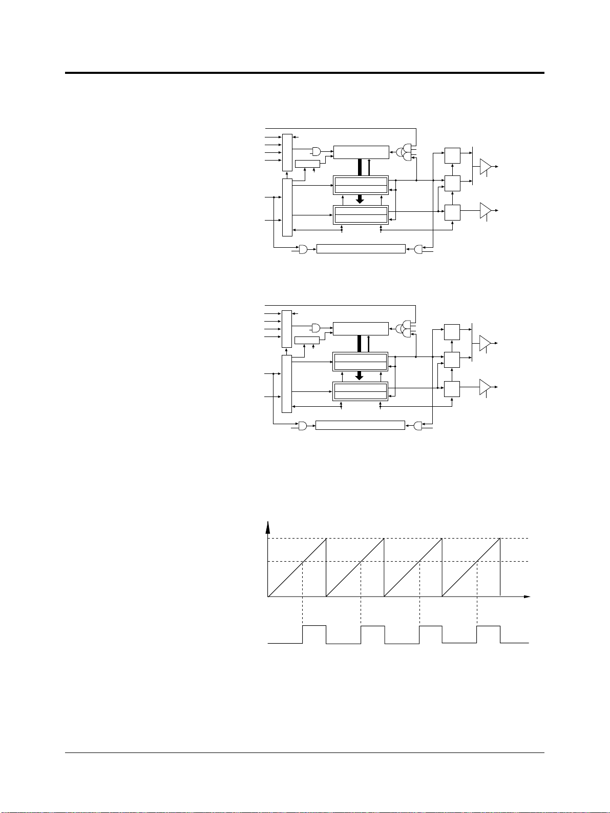
16-Bit Timer Block Diagrams
4.9 16-Bit Timer Block Diagrams
Timers
TM4IC pin
Timer 0 underflow
Timer 1 underflow
TM4IB pin
B
OSC
TM4IB pin
TM4IA pin
TM5IC pin
Timer 0 underflow
Timer 1 underflow
TM5IB pin
B
OSC
TM5IB pin
TM5IA pin
[S]
CLK
TM4BC
TM4CA
TM4CAX
TM4CB
TM4CBX
[MD] [LD]
TM4MD
[TGE]
[EN]
SelectorController
U/D control
[UD]
Capture
Capture
/4
LOAD
CLR
Match
Match
[ECLR]
[LP]
[ONE]
[ASEL]
Q
T
R
R
Q
S
R
Q
T
R
TM4IOA pin
P2MD6,P2DIR6 setting
TM4IOB pin
P2MD5,P2DIR5 setting
Figure 4-15 Timer 4 Block Diagram
[S]
CLK
TM5BC
TM5CA
TM5CAX
TM5CB
TM5CBX
[MD] [LD]
TM5MD
[TGE]
[EN]
SelectorController
U/D control
[UD]
Capture
Capture
/4
LOAD
CLR
Match
Match
[ECLR]
[LP]
[ONE]
[ASEL]
Q
T
R
R
Q
S
R
Q
T
R
TM5IOA pin
P4MD2,P4DIR2 setting
TM5IOB pin
P4MD3,P4DIR3 setting
Figure 4-16 Timer 5 Block Diagram
4.10 16-Bit Timer Timing
BC value
CA
CB
TMnIOA
TMnOA
Figure 4-17 Single-Phase PWM Output Timing (16-Bit Timers)
Time
Panasonic Semiconductor Development Company MN102H75K/F75K/85K/F85K LSI User Manual
90
Panasonic
Page 92

Timers
16-Bit Timer Timing
BC value
New value written
to CCRB
Change reflected in
next clock cycle
CA
CB
Time
TMnIOA
TMnOA
Figure 4-18 Single-Phase PWM Output Timing with Data Change (16-Bit Timers)
BC value
CA
CB
Time
TMnOA
TMnOB
BC value
CA
TMnIB
TMnOA
Figure 4-19 Two-Phase PWM Output Timing (16-Bit Timers)
Time
Figure 4-20 One-Shot Pulse Output Timing (16-Bit Timers)
MN102H75K/F75K/85K/F85K LSI User Manual Panasonic Semiconductor Development Company
91
Panasonic
Page 93

T
T
BC value
Timers
16-Bit Timer Timing
CA
MnIB
MnIA
Figure 4-21 External Count Direction Control Timing (16-Bit Timers)
BC value
MnIB
Time
Time
Figure 4-22 Event Timer Input Timing (16-Bit Timers)
BC value
FFFF
Time
TMnIB
TMnIA
TMnCA
TMnCB
Figure 4-23 Single-Phase Capture Input Timing (16-Bit Timers)
Panasonic Semiconductor Development Company MN102H75K/F75K/85K/F85K LSI User Manual
92
Panasonic
0033 (Example)
5A87 (Example)
Page 94

Timers
16-Bit Timer Timing
BC value
FFFF
Time
TMnIB
TMnIA
TMnCA
TMnCB
Figure 4-24 Two-Phase Capture Input Timing (16-Bit Timers)
BC value
TMnIA
TMnIB
Figure 4-25 Two-Phase 4x Encoder Timing (16-Bit Timers)
BC value
0033 (Example)
5A87 (Example)
Time
Time
TMnIA
TMnIB
Figure 4-26 Two-Phase 1x Encoder Timing (16-Bit Timers)
MN102H75K/F75K/85K/F85K LSI User Manual Panasonic Semiconductor Development Company
93
Panasonic
Page 95

16-Bit Timer Setup Examples
4.11 16-Bit Timer Setup Examples
4.11.1 Setting Up an Event Counter Using Timer 4
In this example, timer 4 counts the TM4IB input signal (B
and generates an interrupt on the second and fifth cycles.
/4 = 6 MHz or less)
OSC
Timers
TM4IB
(B
OSC
TM4IB
/4)
P2
P6
Timer 4
up
Controller
CORE
Interrupts
Timers 0-3
Timers 4-5
A. Chip Level
TM4BC
TM4CA
TM4CAX
TM4CB
TM4CBX
ROM, RAM
Bus Controller
Serial I/Fs
ADC
TQ
R
Q
S
TQ
P4
P5
(TM4OA)
B. Block Level
Figure 4-27 Block Diagram of Event Counter Using Timer 4
■
To set up timer 4:
1. Set the operating mode in the timer 4 mode register (TM4MD). Disable
timer 4 counting and interrupts. Select up counting. Select TM4IB as the
clock source.
Use the MOV instruction for this
setup and only use 16-bit write
operations.
This step stops the TM4BC
count and clears both TM4BC
and the S-R flip-flop to 0.
TM4MD (example) x’00FE80’
Bit:1514131211109876543210
TM4ENTM4
Setting:0000000000010010
NLD
——
TM4
UD1
TM4
UD0
TM4
TGE
TM4
ONE
TM4
MD1
TM4
MD0
TM4
ECLR
TM4LPTM4
ASEL
TM4S2TM4S1TM4
S0
2. Set the divide-by ratio for timer 4. To divide the TM4IB input signa l by 5,
write x’0004’ to timer 4 compare/capture register A (TM4CA). (The valid
range for TM4CA is x’0001’ to x’FFFE’.)
Panasonic Semiconductor Development Company MN102H75K/F75K/85K/F85K LSI User Manual
94
Panasonic
Page 96

Timers
16-Bit Timer Setup Examples
TM4CA (example) x’00FE84’
Bit:1514131211109876543210
TM4
TM4
TM4
TM4
TM4
TM4
TM4
TM4
TM4
TM4
TM4
TM4
TM4
TM4
TM4
CA15
CA14
CA13
CA12
CA11
CA10
CA9
CA8
CA7
CA6
CA5
CA4
CA3
CA2
Setting:0000000000000100
CA1
TM4
CA0
3. Set the phase difference for timer 4. For a 2-cycle phase difference, write
x’0001’ to timer 4 compare/capture reg ister B (TM4CB). (The v alid rang e is
-1 ≤ TM4CB < the TM4CA value.)
TM4CB (example) x’00FE88’
Bit:1514131211109876543210
TM4
TM4
TM4
TM4
TM4
TM4
TM4
TM4
TM4
TM4
TM4
TM4
TM4
TM4
TM4
CB15
CB14
CB13
CB12
CB11
CB10
CB9
CB8
CB7
CB6
CB5
CB4
CB3
CB2
Setting:0000000000000001
CB1
TM4
CB0
4. Set the TM4NLD bit of the TM4MD register to 1 and the TM4EN bit to 0.
This enables TM4BC and the S-R flip-flop. This step ensures stable operation. If it is omitted, the binary counter may not count the first cycle. Do not
change any other operating modes during this step.
5. Set TM4NLD and TM4EN to 1. This starts the timer. Counting begins at the
start of the next cycle.
■
To enable timer 4 capture interrupts:
Cancel all existing interrupt requests. Next, set the interrupt priority level in the
TM4CBLV[2:0] bits of the TM4CBICH register (lev els 0 to 6), set the TM4 CBIE
bit to 1, set the TM4CBIR bit of TM4CBICL to 0, set the TM4CAIE bit of
TM4CAICH to 1, and set the TM4CAIR bit of TM4CAICL to 0. From this point
on, an interrupt request is generated whenever a timer 4 capture A or capture B
event occurs.
Timer 4 can operate as an event counter, but timer 4 does not operate in STOP
mode, when B
. This means that the frequency of the event counter clock must be 1/4 or
B
OSC
is off. If you use an external clock, it must be synchronized to
OSC
less that of the oscillator (6 MHz with a 24-MHz oscillator).
Figure 4-28 shows an example timing chart.
TM4CA
TM4CB
TM4BC
0000 0003 00000001
0002 0004 00030001 0002 0004
0004
0001
TM4IB
Interrupts
B
BA A
Figure 4-28 Event Counter Timing (Timer 4)
MN102H75K/F75K/85K/F85K LSI User Manual Panasonic Semiconductor Development Company
95
Panasonic
Page 97

Timers
16-Bit Timer Setup Examples
4.11.2 Setting Up a Sing le-Phase PWM O utput Signal U sing
Tim e r 4
In this example, timer 4 is used to divide B
single-phase PWM signal. The duty of this signal is 2:3. To accomplish this, the
program must load the divide-by ratio of 5 (actual setting: 4) into compare/
capture register A and a cycle count of 2 (actual setting: 1) into compare/capture
register B.
by 5 and generate a five-cycle,
OSC
TM4OA
B
OSC
P3
P6
PC
P2
CORE
Interrupts
Timers 0-3
Timers 4-5
A. Chip Level
ROM, RAM
Bus Controller
Serial I/Fs
ADC
P4
P5
Timer 4
/4
TM4BC
up
TM4CA
TQ
TM4CAX
R
Q
S
TM4OA
Controller
TM4CB
TQ
TM4CBX
B. Block Level
Figure 4-29 Block Diagram of Single-Phase PWM Output Using Timer 4
■
To set up the output port:
Set the P2MD[13:12] bits of the port 2 output mode register (P2MD) to b’01’
(selecting the TM4IOA pin) and set the P2DIR6 bit of the port 2 I/O control
register (P2DIR) to 1 (selecting output direction). This step selects the TM4OA
pin (P26) as the timer output port.
P2MD (example) x’00FFF4’
Bit:1514131211109876543210
P2
—
MD14P2MD13P2MD12P2MD11P2MD10P2MD9P2MD8P2MD7P2MD6P2MD5P2MD4P2MD3P2MD2P2MD1P2MD0
Setting:0001000000000000
Panasonic Semiconductor Development Company MN102H75K/F75K/85K/F85K LSI User Manual
96
Panasonic
Page 98

Timers
16-Bit Timer Setup Examples
Use the MOV instruction for this
setup and only use 16-bit write
operations.
This step stops the TM4BC
count and clears both TM4BC
and the S-R flip-flop to 0.
P2DIR (example) x’00FFE2’
Bit:76543210
P2
DIR7P2DIR6P2DIR5P2DIR4P2DIR3P2DIR2P2DIR1P2DIR0
Setting:01000000
■ To set up timer 4:
1. Set the operating mode in the timer 4 mode register (TM4MD). Disable
timer 4 counting and interrupts. Select up counting. Select B
OSC
/4 as the
clock source. Select the double-buffer operating mode.
TM4MD (example) x’00FE80’
Bit:1514131211109876543210
TM4ENTM4
Setting:0000000001010011
NLD
——
2. Set the divide-by ratio for timer 4. To divide B
TM4
UD1
TM4
UD0
TM4
TGE
TM4
ONE
TM4
MD1
TM4
MD0
TM4
TM4LPTM4
ECLR
/4 by 5, write x’0004’ to
OSC
TM4S2TM4S1TM4
ASEL
S0
timer 4 compare/capture register A (TM4CA). (The valid range for TM4CA
is x’0001’ to x’FFFE’.)
TM4CA (example) x’00FE84’
Bit:1514131211109876543210
TM4
TM4
TM4
TM4
TM4
TM4
TM4
TM4
TM4
TM4
TM4
TM4
TM4
TM4
TM4
CA15
CA14
CA13
CA12
CA11
CA10
CA9
CA8
CA7
CA6
CA5
CA4
CA3
CA2
Setting:0000000000000100
3. Set the timer 4 duty cycle. For a 2/5 B
/4 duty cycle, write x’0001’ to
OSC
CA1
TM4
CA0
timer 4 compare/capture register B (TM4CB). (The valid range is -1 <
TM4CB < the TM4CA value.)
TM4CB (example) x’00FE88’
Bit:1514131211109876543210
TM4
TM4
TM4
TM4
TM4
TM4
TM4
TM4
TM4
TM4
TM4
TM4
TM4
TM4
TM4
CB15
CB14
CB13
CB12
CB11
CB10
CB9
CB8
CB7
CB6
CB5
CB4
CB3
CB2
Setting:0000000000000001
CB1
TM4
CB0
4. Write a dummy data word (of any value) to TM4CAX. In double-buffer
mode, TM4CA is compared to TM4CAX. The contents of TM4CA are
loaded to TM4CAX when TM4BC = TM4CAX. However, since TM4CAX
is undefined or x’0000’ before this operation starts, this initial dummy write
prevents timing errors.
5. Write a dummy data word (of any value) to TM4CBX. In double-buffer
mode, TM4CB is compared to TM4CBX. The contents of TM4CB are
loaded to TM4CBX when TM4BC = TM4CBX. However, since TM4CBX
is undefined or x’0000’ before this operation starts, this initial dummy write
prevents timing errors.
MN102H75K/F75K/85K/F85K LSI User Manual Panasonic Semiconductor Development Company
97
Panasonic
Page 99

Timers
16-Bit Timer Setup Examples
6. Set the TM4NLD bit of the TM4MD register to 1 and the TM4EN bit to 0.
This enables TM4BC and the S-R flip-flop. This step ensures stable operation. If it is omitted, the binary counter may not count the first cycle. Do not
change any other operating modes during this step.
7. Set TM4NLD and TM4EN to 1. This starts the timer. Counting begins at the
start of the next cycle.
Timer 4 can output a single-phase PWM signal at any d uty. You must select up
counting. Timer 4 does not operate in STOP mode, when B
an external clock, it must be synchr oni zed to B
OSC
.
is off. If you use
OSC
In this procedure, you set the cycle (x’0001’ to x’FFFE’) in the TM4CA register
and the duty in the TM4CB register. When the contents of TM4BC match those
of the TM4CB register , the S-R flip-flop resets at the begin ning of the ne xt c ycle.
Please note the following:
■ When -1 ≤ TM4CB < TM4CA, TM4OA output is low during the 0 to
TM4CB + 1 cycles of the TM4CA + 1 cycle period and high during the
remainder of the cycles.
■ When TM4CA ≤ TM4CB ≤ x’FFFE, TM4OA output is always low.
■ When TM4BC = x’FFFF’, TM4OA output is always high.
The circuitry is configured so that there are no waveform errors, even when the
output is always high or always low. Counting begins after the TM 4EN bit is set
in the TM4MD register.
Panasonic Semiconductor Development Company MN102H75K/F75K/85K/F85K LSI User Manual
98
Panasonic
Page 100

Timers
16-Bit Timer Setup Examples
Figure 4-30 below shows the output waveforms for TM4OA. Both A and B
interrupts can occur, but B interrupts can only occur if the TM4CB setting is from
0 to less than TM4CA. This is because when TM4CB ≤ TM4CA, TM4BC never
matches TM4CB.
Write to TM4MD
TM4EN
TM4BC
/4
B
OSC
CLRBC4
(1) TMCB = 4 (All 0s)
S4
R4
012340 01234012340123
TM4OA
Interrupts
(2) TMCB = 2
S4
R4
TM4OA
Interrupts
(3) TMCB = FFFF (All 1s)
S4
R4
TM4OA
Interrupts
0s on first cycle, since
S4 has not gone high yet.
Figure 4-30 Single-Phase PWM Output Timing (Timer 4)
AB
A
B
A
AB
A
B
A
AB
A
B B
A
MN102H75K/F75K/85K/F85K LSI User Manual Panasonic Semiconductor Development Company
99
Panasonic
 Loading...