


Service Manual
15-inch LCD Monitor
H15AAU/R
Service Manual Versions and Revision
No. |
Ve rsion |
Re le ase Date |
Re vis ion |
|
|
|
|
1. |
1.0 |
Jan. 31, 2002 |
Original release |
|
|
|
|
Copyright
Copyright 2002 LiteOn Technology Corp.
All Rights Reserved
This manual may not, in whole or in part, be copied, photocopied, reproduced, translated, or converted to any electronic or machine readable form without prior written permission of LiteOn Technology Corp.
H15AAU / H15AAR Service Manual.
Trademarks
LiteOn is a registered trademark of LiteOn Technology Corp.
All other trademarks are the property of their respective owners.
Printed in Taiwan.

|
|
Table of Contents |
|
1. |
Audio circuit --------------------------------------------------------------------------------------------------------------- |
1 |
|
|
1.1 |
Audio input ------------------------------------------------------------------------------------------------------------ |
1 |
|
1.2 |
Audio output ---------------------------------------------------------------------------------------------------------- |
1 |
2. |
Power supply -------------------------------------------------------------------------------------------------------------- |
1 |
|
3. |
On-screen circuit ---------------------------------------------------------------------------------------------------------- |
2 |
|
4. |
Video input circuit -------------------------------------------------------------------------------------------------------- |
2 |
|
5. |
Definition converter LSI peripheral circuit ---------------------------------------------------------------------------- |
2 |
|
6. |
System reset, LED control circuit --------------------------------------------------------------------------------------- |
2 |
|
7. |
E2PROM for PNP --------------------------------------------------------------------------------------------------------- |
2 |
|
8. |
E2PROM -------------------------------------------------------------------------------------------------------------------- |
3 |
|
9. |
CPU circuit ----------------------------------------------------------------------------------------------------------------- |
3 |
|
|
9.1 |
Dection of POWER switch status ---------------------------------------------------------------------------------- |
3 |
|
9.2 |
Display mode identification ----------------------------------------------------------------------------------------- |
3 |
|
9.3 |
User control ----------------------------------------------------------------------------------------------------------- |
4 |
|
9.4 |
Control of identification converter LSI ---------------------------------------------------------------------------- |
5 |
|
9.5 |
I2C bus control -------------------------------------------------------------------------------------------------------- |
5 |
|
9.6 |
Power ON sequence -------------------------------------------------------------------------------------------------- |
6 |
|
9.7 |
Power OFF sequence ------------------------------------------------------------------------------------------------- |
7 |
10. Inverter ---------------------------------------------------------------------------------------------------------------------- |
8 |
||
Circuit Description

H15AAU / H15AAR
1. Audio circuit (Circuit diagrams Main PWB)
1.1Audio input
The audio signal input received from the audio input terminal (JK011) is applied to the amplifier I001 of 4 (L- CH) and 9 (R-CH) through the low-pass filter consisting of R040, R041, R042, R043, C040 and C041.
In this amplifier, controls of Volume and mute are conducted. The audio signal controlled at the pin 6 determines the attenuation of output of the amplifiers. Since then, the signal is output to the jack P003.
1.2Audio output
The audio signal is output from P002 output terminal of the Audio block to the internal speaker system.
2. Power supply (Circuit daigrams MAIN PWB)
2.1Line filter consists of C801, T801, C802, C803, C804. It eliminates high frequency interference to meet EMI’s requirement.
2.2Rec & Filter :
Bridge diode D801 converts AC source into pulsed DC. This pulsed DC is smoothed and filtered by C805. R802 is an NTC ( negative thermal coefficient ) resistor, used to reduce inrush current to be within safe range.
2.3Power transformer :
T802 converts energy for square wave from power source C805 to secondary side to generate +12V and +5V.
2.4Output :
The square wave from T802 is rectified by D809, D810, then filtered by C817, C822 to generate +12V and +5V respectively.
2.4.1A 5V power supply for LCD module, CPU and logic is generated from the power source.
2.4.2I308 : 3-terminal regulator
A 3.3V power supply for I306 analog is generated from the 5V source. 2.4.3 I308 : 3-terminal regulator
A 3.3V power supply for I306 digital is generated from the 5V source.
Q302, Q303 ON/OFF control for LCD Module
ON/OFF control is performed for power ON/OFF and also for the power saving sequence.
2.5Driver :
Q803 drive T802 from PWM control of I801 for power converted.
2.6FB :
Negative feedback CKT consists of photo coupler I802 and adjustable regulator I803. It can maintain output voltages +5V and +12V at a stable level.
2.7PWM :
2.7.1Start : When power is turned on, Q801 conducts due to bias from C805 and R805,R803. C807 is charged a 16 volt and a starting current about 0.3mA to pin 7 of I801. I801 starts to oscillate and outputs a pulse train
through pin 6 to drive Q803.
2.7.2OPP : When Q803 turns on, C805 supplies a linearly increasing triangle current through the primary induc tance of T802 to the driver Q803, once the peak value of this current multiplied by R811 exceeds1 volt, pulse train will be shut down immediately to protect Q803, T802 from being burned out.
2.7.3Regulation : If output voltage +5V goes up, the R terminal of I803 gets more bias, accordingly photo transis tor and photo diode flows more current. The voltage of pin 2 goes up too, making the pulse width of pin 6 to become narrower. So the output voltage +5V will be pulled down to a stable value.
Circuit Description |
Page 1 |
H15AAU / H15AAR
2.7.4OVP : If +5V goes up too much, the induced voltage on pin 4 of T802 becomes large also. Suppose that it is over 18 volts, ZD801 conducts, pin 3 of I801 is pulled up over 1 volt. The pulse train at pin 6 goes down to zero, shutting Q803 off immediately.
2.7.5SCP : If output terminal is short to ground, photo transistor does not conduct, hence Q806 does not conduct either. Then oscillation of I801 is stop, shutting Q803 off immediately.
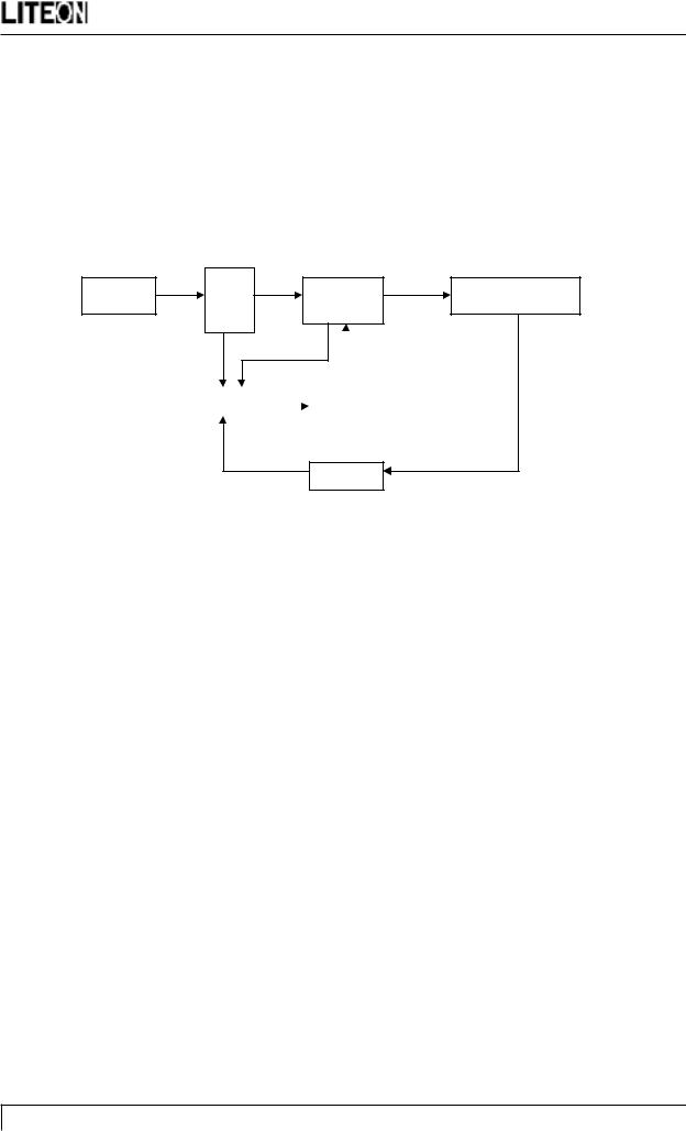
H15AAU / H15AAR Power Board Block Diagram
Rec.
Line Filter Power Output Rec. & Filter
&
Transformer
Filter
|
|
|
|
|
PWM |
|
|
Driver |
|
|
|
|||
|
|
|
|
|
FB
3. On-screen circuit (Circuit diagrams Main PWB)
I300 Embeded function.
On-screen menu screen is established and the resultant data are output from I300 (Circuit diagram MAIN PWB).
4. Video input circuit (Circuit diagram MAIN PWB)
The AC-coupled video signal is used to clamp the black level at 0V).
5. Definition converter LSI peripheral circuit (Circuit diagram MAIN PWB)
I301 MRT V2 gmZAN1 is the definition A/D converter LSI.
The analog R, G, B signal input entered from the video input circuit is converted into the digital data of video signal through the incorporated A/D converter. Based on this conversion, this device performs interpolation during pixel extension. The source voltage for this device is 3.3V and the system clock frequency is 12MHz.
The withstand voltage level for the input signal voltage is 3.3V and 5V.
6. System reset, LED control circuit (Circuit diagram MAIN PWB)
6.1System reset
System reset is performed by detecting the rising and falling of the 5V source voltage at I302.
6.2LED control circuit
Green / amber is lit with the control signal of the LED GREEN and LED AMBER signal pin 43, 42 from I303 (Circuit diagram MAIN PWB).
7. E2PROM for PnP (Circuit diagram MAIN PWB)
Page 2 |
Circuit Description |

H15AAU / H15AAR
8. E2PROM (Circuit diagram MAIN PWB)
Data transfer between I304 and CPU (Circuit diagram MAIN PWB page 4/7 (I303) is effected through the IIC bus SCL (pin 9) and SDA (pin 8) of I300 or SCL (pin 42) and SDA pin 39 of I301. The data to be transferred to each device are stored in I304.
lI300 control data.
lOSD related setting data.
lOther control data for service menu.
9.CPU circuit (Circuit diagram MAIN PWB)
I303 (MTV312M64) (SM89516C25) or (W78E62BP-40) functions as the CPU.
The source voltage for the device is 5.0V and the system clock frequency is 12MHz.
9.1Detection of POWER switch status
The CPU identifies the ON status of the two power supplies. The identification is made when the power supply is turned off. For example, if the power supply is turned off with the POWER switch, the POWER switch must be turned on when activating the power supply again. If the power supply is turned off by pulling out the power cord, then this power supply can be turned on by connecting the power cord, without pressing the POWER switch.
9.2Display mode identification
9.2.1Functions
(1) Display mode identification
lThe display mode of input signal is identified based on Table 1, and according to the frequency and polarity (HPOL, VPOL) of horizontal or vertical sync signal, presence of the horizontal or vertical sync signal, and the discrimination signal (HSYNC_DETECT, VSYNC_DETECT).
lWhen the mode has been identified through the measurement of horizontal and vertical frequencies, the total number of lines is determined with a formula of “ Horizontal frequency / Vertical frequency = Total number of lines. “Final identification can be made by examining the coincidence of the obtained figure with the number of lines for the mode identified from the frequency.
lWhen the detected frequency if the sync signal has changed, the total number of lines should be counted even through it is rge identified frequency in the same mode. Then, it is necessary to examine whether the preset value for the vertical display position of Item 4-3 has exceeded the total number of lines. If exceeded, a maximum value should be set up, which does not exceed the vertical display position of Item 4-3.
(2) Out-of -range
This out-of-range mode is assumed when the frequency of the horizontal / vertical signal is as specified below.
lVertical frequency : Below 50Hz or above 85Hz
lHorizontal frequency : Below 24 KHz or above 75 KHz
(3) Power save mode
The power save mode is assumed when the horizontal / vertical signals are as specified below.
lIf there is no horizontal sync signal input.
lIf there is no vertical sync signal input.
lIf the horizontal sync signal is outside the measuring range of I300.
lIf the vertical sync signal is outside the measuring range of I300.
Circuit Description |
Page 3 |

H15AAU / H15AAR
Table 1
Mode |
No |
Resolution |
H-freq |
Band Width |
Polarity |
||
|
|
|
|
(KHz) |
(MHz) |
H |
V |
|
|
|
|
|
|
||
|
|
|
|
|
|
|
|
1. |
247 |
VGA 720 x 350 |
70Hz |
31.47 |
28.322 |
+ |
- |
|
|
|
|
|
|
|
|
2. |
102 |
VGA 720 x 400 |
70Hz |
31.47 |
28.322 |
- |
+ |
3. |
103 |
VGA 640 x 480 |
60Hz |
31.47 |
25.175 |
- |
- |
|
|
|
|
|
|
|
|
4. |
182 |
MAC 640 x 480 |
66Hz |
35 |
32.24 |
- |
- |
|
|
|
|
|
|
|
|
5. |
173 |
VESA 640 X 480 |
72Hz |
37.86 |
31.5 |
- |
- |
6. |
109 |
VESA 640 X 480 |
75Hz |
37.5 |
31.5 |
- |
- |
|
|
|
|
|
|
|
|
7. |
104 |
VESA 800 x 600 |
56Hz |
35.16 |
36 |
+ |
+ |
|
|
|
|
|
|
|
|
8. |
116 |
VESA 800 x 600 |
60Hz |
37.88 |
40 |
+ |
+ |
|
|
|
|
|
|
|
|
9. |
110 |
VESA 800 x 600 |
75Hz |
46.88 |
49.5 |
+ |
+ |
|
|
|
|
|
|
|
|
10. |
117 |
VESA 800 x 600 |
72Hz |
48.08 |
50 |
+ |
+ |
|
|
|
|
|
|
|
|
11. |
108 |
MAC 832 x 624 |
75Hz |
49.72 |
57.283 |
- |
- |
|
|
|
|
|
|
|
|
12. |
118 |
VESA 1024 x 768 |
60Hz |
48.36 |
65 |
- |
- |
|
|
|
|
|
|
|
|
13. |
217 |
SUN 1024 x 768 |
65Hz |
52.45 |
70.49 |
- |
- |
|
|
|
|
|
|
|
|
14. |
157 |
VESA 1024 x 768 |
70Hz |
56.48 |
75 |
- |
- |
|
|
|
|
|
|
|
|
15. |
141 |
VESA 1024 x 768 |
75Hz |
60.02 |
78.75 |
+ |
+ |
|
|
|
|
|
|
|
|
Attention :
1.When resolution beyond 1024 x 768 is inputted, resolution is lowered with Down scaling to 1024 x 768, and indicated, and OSD should indicate OUT of Range.
9.3User Control
9.3.1 Related ports of I303
Port |
Pin No. |
I/O |
Signal name |
|
Function |
|
|
Remarks |
|
|
|
|
|
|
|||
P1.5 |
7 |
I |
POWER |
Power switch input |
Power ON , OFF |
|||
|
|
|
|
|
|
control |
||
|
|
|
|
|
|
|
|
|
P1.1 |
3 |
I |
DOWN |
|
switch input |
( |
|
) key |
P1.0 |
2 |
I |
UP |
|
switch input |
( |
|
) key |
P1.3 |
5 |
I |
- |
- |
switch input |
( |
- |
) key |
P1.2 |
4 |
I |
+ |
+ |
switch input |
( |
+ |
) key |
Page 4 |
Circuit Description |

H15AAU / H15AAR
9.3.2Functions
Control is effected for the push-switches to be used when the user changes the parameters, in order to modify the respective setting values. Whether the switch has been pressed is identified with the switch input level that is turned “L”.
Each switch input port is pulled up at outside of ASIC.
Each parameter is stored in the EEPROM, the contents of which are updated as required.
9.4 Control of definition converter LSI I300. 9.4.1 Ports related to control
Pin No. |
I/O |
Signal name |
Function |
159 |
I |
IRQ |
interrupt signal |
5 |
I/O |
SCL |
serial clock |
6 |
I/O |
SDA |
serial data |
9.4.2Functions
Major function of I300 are as follows:
(1)Expansion of the display screen.
(2)Timing control for various signal types.
(3)Power-supply sequence (LCD panel).
9.5I2C bus control
9.5.1 Related ports of I303
Port |
Pin No. |
I/O |
Signal name |
Function |
P1.7 |
14 |
O |
SCL |
IIC bus clock |
P1.6 |
13 |
I/O |
SDA |
IIC bus data |
9.5.2I2C-controlled functions
The following functional controls are effected by I2C.
(1) Control of EEPROM I304 for parameter setting.
Circuit Description |
Page 5 |

H15AAU / H15AAR
9.6Power ON sequence
When the POWER switch is pressed, the POWER OFF signal is turned “H”. When this “H” potential is detected, the CPU begins to establish the respective power supplies according to the sequence shown below.
POWER
PPWR
D-SHCLK
INV_EN
LED
DATA
Page 6 |
Circuit Description |
 Loading...