

Linear Technology LTC1291BIJ8, LTC1291BCN8, LTC1291DMJ8, LTC1291DIN8, LTC1291DIJ8 Datasheet
...
LTC1291
CODE
0
–0.5
DELTA (LSB)
–0.4
–0.2
–0.1
0
0.5
0.2
1024
2048
2560
1291 TA02
–0.3
0.3
0.4
0.1
512 1536
3072
3584
4096
Single Chip 12-Bit
Data Acquisition System
EATU
F
■
Built-In Sample-and-Hold
■
Single Supply 5V Operation
■
Power Shutdown
■
Direct 3- or 4-Wire Interface to Most MPU Serial
RE
S
Ports and All MPU Parallel Ports
■
Two-Channel Analog Multiplexer
■
Analog Inputs Common Mode to Supply Rails
■
8-Pin DIP Package
U
KEY SPECIFICATIO S
■
Resolution: 12 Bits
■
Fast Conversion Time: 12µs Max Over Temp.
■
Low Supply Current:
6.0mA (Typ) Active Mode
10µA (Max) Shutdown Mode
DUESCRIPTIO
The LTC1291 is a data acquisition system that contains a
serial I/O successive approximation A/D converter. It uses
LTCMOSTM switched capacitor technology to perform a
12-bit unipolar A/D conversion. The input multiplexer can
be configured for either single-ended or differential inputs. An on-chip sample-and-hold is included on the “+”
input. When the LTC1291 is idle, it can be powered down
in applications where low power consumption is desired.
An external reference is not required because the LTC1291
takes its reference from the power supply (VCC). All these
features are packaged in an 8-pin DIP.
The serial I/O is designed to communicate without external
hardware to most MPU serial ports and all MPU parallel
I/O ports allowing data to be transmitted over three or four
wires. Given the accuracy, ease of use and small package
size, this device is well suited for digitizing analog signals
in remote applications where minimum number of interconnects, small physical size, and low power consumption are important.
TM
LTCMOS
is a trademark of Linear Technology Corporation
2-CHANNEL
MUX*
U
O
A
PPLICATITYPICAL
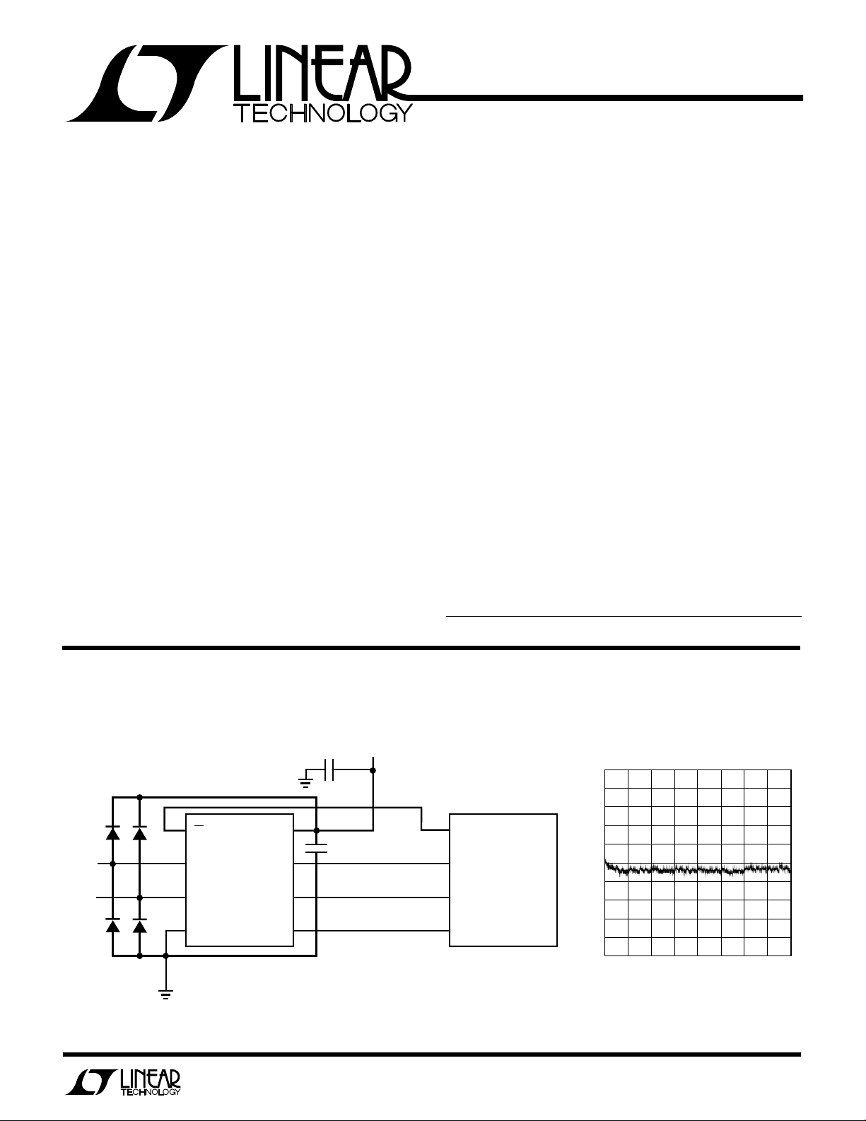
2-Channel 12-Bit Data Acquisition System
22µF
TANTALUM
+5V
+
)
LTC1291
V
CC(VREF
D
CLK
OUT
D
0.1µF
IN
AND GND WITH 1N4148 DIODES.
CC
< GND OR V
IN
> VCC). SEE
IN
CS
CH0
CH1
GND
*FOR OVERVOLTAGE PROTECTION LIMIT THE INPUT CURRENT TO 15mA
PER PIN OR CLAMP THE INPUTS TO V
CONVERSION RESULTS ARE NOT VALID WHEN THE SELECTED CHANNEL OR
THE OTHER CHANNEL IS OVERVOLTAGED (V
SECTION ON OVERVOLTAGE PROTECTION IN THE APPLICATIONS INFORMATION.
Channel-to-Channel
INL Matching
DO
SCK
MC68HC11
MISO
MOSI
1291 TA01
1
LTC1291
O
A
(Notes 1 and 2)
LUTEXI T
S
W
A
WUW
ARB
U
G
I
S
PACKAGE
/
O
RDER I FOR ATIO
Supply Voltage (VCC) to GND.................................. 12V
Voltage
Analog Inputs............................ –0.3V to V
Digital Inputs........................................ –0.3V to 12V
Digital Outputs .......................... –0.3V to V
Power Dissipation............................................. 500mW
Operating Temperature Range
LTC1291BC, LTC1291CC,
LTC1291DC............................................ 0°C to 70°C
LTC1291BI, LTC1291CI,
LTC1291DI ........................................ –40°C to 85°C
CC
CC
+ 0.3V
+ 0.3V
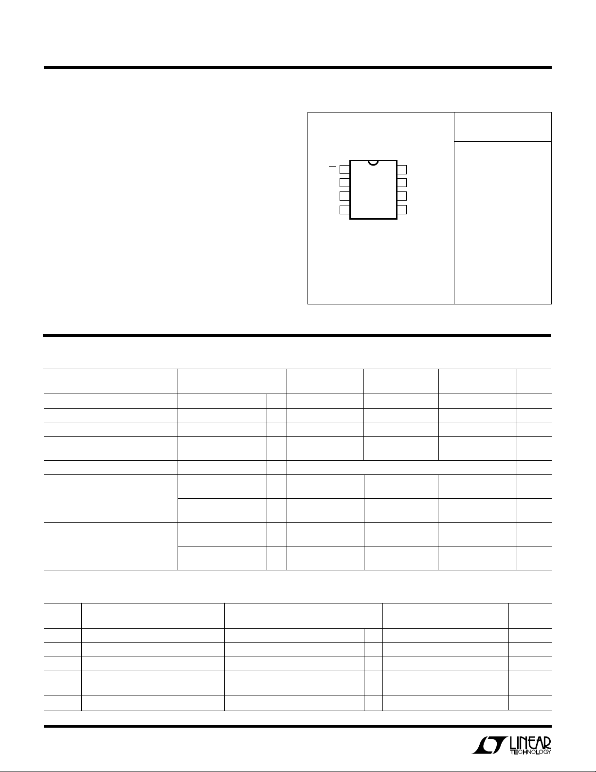
TOP VIEW
1
CS
2
CH0
3
CH1
45
GND
J8 PACKAGE
8-LEAD CERAMIC DIP
N8 PACKAGE
8-LEAD PLASTIC DIP
LTC1291BM, LTC1291CM,
LTC1291DM................................... –55°C to 125°C
Storage Temperature Range ................ –65°C to 150°C
Lead Temperature (Soldering, 10 sec.)................ 300°C
UU W
CO VERTER A D ULTIPLEXER CHARACTERISTICS
V
CC (VREF
CLK
D
OUT
D
IN
(Note 3)
)
8
7
6
WU
ORDER PART
NUMBER
LTC1291BMJ8
LTC1291CMJ8
LTC1291DMJ8
LTC1291BIJ8
LTC1291CIJ8
LTC1291DIJ8
LTC1291BIN8
LTC1291CIN8
LTC1291DIN8
LTC1291BCN8
LTC1291CCN8
LTC1291DCN8
U
PARAMETER CONDITIONS MIN TYP MAX MIN TYP MAX MIN TYP MAX UNITS
Offset Error (Note 4) ● ±3.0 ±3.0 ±3.0 LSB
Linearity Error (INL) (Note 4 & 5) ● ±0.5 ±0.5 ±0.75 LSB
Gain Error (Note 4) ● ±1.0 ±2.0 ±4.0 LSB
Minimum Resolution for which No
Missing Codes are Guaranteed
Analog Input Range (Note 7) V
On Channel Leakage Current On Channel = 5V
(Note 8) Off Channel = 0V
On Channel = 0V
Off Channel = 5V
Off Channel Lekage Current On Channel = 5V
(Note 8) Off Channel = 0V
On Channel = 0V ● ±1 ±1 ±1 µA
Off Channel = 5V
AC CHARACTERISTICS
SYMBOL PARAMETER CONDITIONS MIN TYP MAX UNITS
f
CLK
t
SMPL
t
CONV
t
CYC
t
dDO
Clock Frequency VCC = 5V (Note 6) (Note 9) 1.0 MHz
Analog Input Sample Time See Operating Sequence 2.5 CLK Cycles
Conversion Time See Operating Sequence 12 CLK Cycles
Total Cycle Time See Operating Sequence (Note 6) 18 CLK Cycles
Delay Time, CLK↓ to D
OUT
(Note 3)
Data Valid See Test Circuits ● 160 300 ns
● 12 12 12 Bits
● ±1 ±1 ±1 µA
● ±1 ±1 ±1 µA
● ±1 ±1 ±1 µA
LTC1291B
LTC1291C
–0.05V to VCC + 0.05V
LTC1291B/LTC1291C/LTC1291D
+ 500ns
LTC1291D
2
LTC1291
AC CHARACTERISTICS
SYMBOL PARAMETER CONDITIONS MIN TYP MAX UNITS
t
dis
t
en
t
hDI
t
hDO
t
WHCLK
t
WLCLK
t
f
t
r
t
suDI
t
suCS
t
WHCS
t
WLCS
C
IN
Delay Time, CS↑ to D
Delay Time, CLK↓ to D
Hold Time, DIN after CLK↑ VCC = 5V (Note 6) 50 ns
Time Output Data Remains Valid after CLK↓ 130 ns
CLK High Time VCC = 5V (Note 6) 300 ns
CLK Low Time VCC = 5V (Note 6) 400 ns
D
Fall Time See Test Circuits ● 65 130 ns
OUT
D
Rise Time See Test Circuits ● 25 50 ns
OUT
Setup Time, DIN Stable before CLK↑ VCC = 5V (Note 6) 50 ns
Setup Time, CS↓ before CLK↑ VCC = 5V (Note 6) 50 ns
CS High Time During Conversion VCC = 5V (Note 6) 500 ns
CS Low Time During Data Transfer VCC = 5V (Note 6) 18 CLK Cycles
Input Capacitance Analog Inputs On Channel 100 pF
OUT
OUT
(Note 3)
LTC1291B/LTC1291C/LTC1291D
Hi-Z See Test Circuits ● 80 150 ns
Enabled See Test Circuits ● 80 200 ns
Analog Inputs Off Channel 5 pF
Digital Inputs 5 pF
U
D
DIGITAL
SYMBOL PARAMETER CONDITIONS MIN TYP MAX UNITS
V
IH
V
IL
I
IH
I
IL
V
OH
V
OL
I
OZ
I
SOURCE
I
SINK
I
CC
The
● denotes specifications which apply over the operating temperature
range; all other limits and typicals TA = 25°C.
Note 1: Absolute Maximum Ratings are those values beyond which the life
of a device may be impaired.
Note 2: All voltage values are with respect to ground (unless otherwise
noted).
Note 3: V
Note 4: One LSB is equal to V
5V, 1LSB = 5V/4096 = 1.22mV.
Note 5: Linearity error is specified between the actual end points of the
A/D transfer curve. The deviation is measured from the center of the
quantization band.
Note 6: Recommended operating conditions.
CC
A
High Level Input Voltage VCC = 5.25V ● 2.0 V
Low Level Input Voltage VCC = 4.75V ● 0.8 V
High Level Input Current VIN = V
Low Level Input Current VIN = 0V ● –2.5 µA
High Level Output Voltage VCC = 4.75V, I
Low Level Output Voltage VCC = 4.75V, I
High Z Output Leakage V
Output Source Current V
Output Sink Current V
Positive Supply Current CS High ● 612 mA
= 5V, CLK = 1.0MHz unless otherwise specified.
DC
divided by 4096. For example, when VCC =
CC
LECTRICAL C CHARA TER ST
E
CC
= –10µA 4.7 V
OUT
VCC = 4.75V, I
= VCC, CS High ● 3 µA
OUT
V
= 0V, CS High ● –3 µA
OUT
= 0V –20 mA
OUT
= V
OUT
CS High
Power shutdown
CLK Off
= – 360µA ● 2.4 4.0 V
OUT
= 1.6mA ● 0.4 V
OUT
CC
LTC1291BC, LTC1291CC, LTC1291DC ● 510 µA
LTC1291BI, LTC1291CI, LTC1291DI,
LTC1291BM, LTC1291CM, LTC1291DM
Note 7: Two on-chip diodes are tied to each analog input which will
conduct for analog voltages one diode drop below GND or one diode drop
above VCC. Be careful during testing at low VCC levels (4.5V), as high level
analog inputs (5V) can cause this input diode to conduct, especially at
elevated temperature, and cause errors for inputs near full scale. This spec
allows 50mV forward bias of either diode. This means that as long as the
analog input does not exceed the supply voltage by more than 50mV, the
output code will be correct.
Note 8: Channel leakage current is measured after the channel selection.
Note 9: Increased leakage currents at elevated temperatures cause the
S/H to droop, therefore it is recommended that f
f
CLK
I
≥ 30kHz at 85°C and f
(Note 3)
ICS
LTC1291B/LTC1291C/LTC1291D
● 2.5 µA
20 mA
● 515 µA
≥ 125kHz at 125°C,
≥ 3kHz at 25°C.
CLK
CLK
3
LTC1291
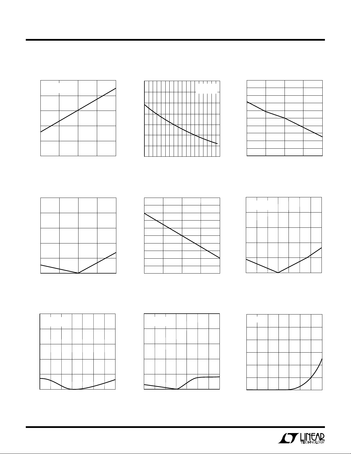
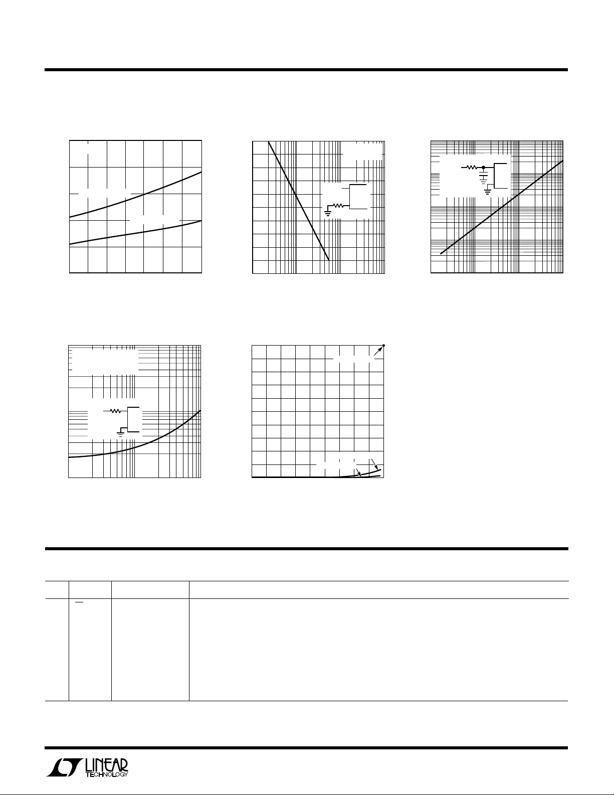
AMBIENT TEMPERATURE (°C)
–50
MINIMUM CLK FREQUENCY* (MHz)
0.15
0.20
0.25
50
1291 G09
0.10
0.05
–25
0
25
75
125100
VCC = 5V
LPER
Supply Current vs Supply Voltage
10
CLK = 1MHz
= 25°C
T
A
8
6
4
SUPPLY CURRENT (mA)
2
0
4
SUPPLY VOLTAGE (V)
F
5
O
R
ATYPICA
6
1291 G01
UW
CCHARA TERIST
E
C
Supply Current vs Temperature
10
9
8
7
6
5
SUPPLY CURRENT (mA)
4
3
–50
–30 –10
AMBIENT TEMPERATURE (°C)
10
ICS
50 90
30 70
CLK = 1MHz
= 5V
V
CC
110
1291 G02
130
Change in Offset vs Supply
Voltage
))
0.5
REF
0.4
(V
CC
0.3
0.2
0.1
0
–0.1
–0.2
–0.3
–0.4
–0.5
CHANGE IN OFFSET (LSB = 1/4096 × V
4.0
4.5
5.0
SUPPLY VOLTAGE (V)
5.5
6.0
1291 G03
Change in Linearity vs Supply
Voltage
))
0.5
REF
(V
CC
0.4
0.3
0.2
0.1
0
CHANGE IN LINEARITY (LSB = 1/4096 × V
4.0
4.5
5.0
SUPPLY VOLTAGE (V)
Change in Linearity vs
Temperature
0.5
VCC = 5V
CLK = 1MHz
0.4
0.3
5.5
1291 G04
6.0
Change in Gain Error vs Supply
Voltage Change in Offset vs Temperature
))
(V
CHANGE IN GAIN ERROR (LSB = 1/4096 × V
REF
CC
–0.1
–0.2
–0.3
–0.4
–0.5
0.5
0.4
0.3
0.2
0.1
0
4.0
4.5
5.0
SUPPLY VOLTAGE (V)
5.5
6.0
1291 G05
0.5
VCC = 5V
CLK = 1MHz
0.4
0.3
0.2
0.1
MAGNITUDE OF OFFSET CHANGE (LSB)
0
–50
0
–25
AMBIENT TEMPERATURE (°C)
50
25
Minimum Clock Rate for
Change in Gain vs Temperature
0.5
VCC = 5V
CLK = 1MHz
0.4
0.3
0.1 LSB Error
100
125
1291 G06
75
0.2
0.1
MAGNITUDE OF LINEARITY CHANGE (LSB)
0
–50
–25
AMBIENT TEMPERATURE (°C)
* AS THE CLK FREQUENCY IS DECREASED FROM 1MHz, MINIMUM CLK FREQUENCY (∆ERROR ≤ 0.1LSB) REPRESENTS THE
FREQUENCY AT WHICH A 0.1LSB SHIFT IN ANY CODE TRANSITION FROM ITS 1MHz VALUE IS FIRST DETECTED.
4
0.2
0.1
MAGNITUDE OF GAIN CHANGE (LSB)
0
0
75
50
25
100
125
1291 G07
–50
0
–25
AMBIENT TEMPERATURE (°C)
50
25
75
100
125
1291 G08
LPER
F
O
R
ATYPICA
UW
CCHARA TERIST
E
C
LTC1291
ICS
D
Delay Time vs Temperature
OUT
250
VCC = 5V
200
MSB-FIRST DATA
150
0
LSB-FIRST DATA
25
50
DELAY TIME FROM CLK↓ (ns)
OUT
D
100
50
0
–50
–25
AMBIENT TEMPERATURE (°C)
Sample-and-Hold Acquisition
Time vs Source Resistance
100
VCC = 5V
= 25°C
T
A
0V TO 5V INPUT STEP
R
+
SOURCE
10
S/H AQUISITION TIME TO 0.02% (µs)
1
100
V
IN
+
–
1k 10k
R
+ (Ω)
SOURCE
Maximum Clock Rate vs Source
Resistance
1.0
0.8
0.6
0.4
0.2
MAXIMUM CLK FREQUENCY* (MHz)
75
125100
1291 G10
0
100
1k 10k 100k
R
SOURCE
+V
R
SOURCE
–
(Ω)
VCC = 5V
CLK = 1MHz
IN
–
+
+IN
–IN
–
1291 G11
Maximum Filter Resistor vs
Cycle Time
10k
R
FILTER
1k
** (Ω)
FILTER
100
10
MAXIMUM R
1
10
+V
C
FILTER
IN
≥1µF
+
–
100
CYCLE TIME (µs)
1k
10k
1291 G12
Input Channel Leakage Current
vs Temperature
1000
1291 G13
900
800
700
600
500
400
300
200
100
INPUT CHANNEL LEAKAGE CURRENT (nA)
0
–30 10
–10
–50
AMBIENT TEMPERATURE (°C)
GUARANTEED
ON CHANNEL
OFF CHANNEL
70 90
50 130
30
110
1291 G14
* MAXIMUM CLK FREQUENCY REPRESENTS THE CLK
FREQUENCY AT WHICH A 0.1LSB SHIFT IN THE
ERROR AT ANY CODE TRANSITION FROM ITS 1MHz
VALUE IS FIRST DETECTED.
**MAXIMUM R
VALUE AT WHICH A 0.1LSB CHANGE IN FULL SCALE
ERROR FROM ITS VALUE AT R
DETECTED.
REPRESENTS THE FILTER RESISTOR
FILTER
= 0Ω IS FIRST
FILTER
U
UU
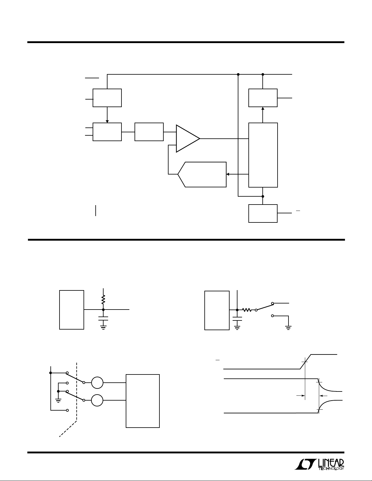
PI FU CTIO S
# PIN FUNCTION DESCRIPTION
1 CS Chip Select Input A logic low on this input enables the LTC1291.
2, 3 CH0, CH1 Analog Inputs These inputs must be free of noise with respect to GND.
4 GND Analog Ground GND should be tied directly to an analog ground plane.
5D
6D
IN
OUT
7 CLK Shift Clock This clock synchronizes the serial data transfer.
8V
CC(VREF
Digital Data Input The multiplexer address is shifted into this input.
Digital Data Output The A/D conversion result is shifted out of this output.
) Positive Supply and This pin provides power and defines the span of the A/D converter. This supply must be kept free of noise and
Reference Voltage ripple by bypassing directly to the analog ground plane.
5
LTC1291
D
OUT
WAVEFORM 1
(SEE NOTE 1)
2.0V
t
dis
90%
10%
D
OUT
WAVEFORM 2
(SEE NOTE 2)
CS
NOTE 1: WAVEFORM 1 IS FOR AN OUTPUT WITH INTERNAL CONDITIONS SUCH
THAT THE OUTPUT IS HIGH UNLESS DISABLED BY THE OUTPUT CONTROL.
NOTE 2: WAVEFORM 2 IS FOR AN OUTPUT WITH INTERNAL CONDITIONS SUCH
THAT THE OUTPUT IS LOW UNLESS DISABLED BY THE OUTPUT CONTROL.
1291 TC06
BLOCK
IDAGRA
8
)
V
CC (VREF
W
7
CLK
D
IN
CH0
CH1
TEST CIRCUITS
5
2
3
GND
INPUT
SHIFT
REGISTER
ANALOG
INPUT MUX
4
SAMPLE
AND
HOLD
COMP
12-BIT
CAPACITIVE
DAC
OUTPUT
SHIFT
REGISTER
12-BIT
SAR
CONTROL
AND
TIMING
6
1
1291 BD
D
OUT
CS
Load Circuit for t
1.4V
D
OUT
3k
dDO
100pF
, tr and t
On and Off Channel Leakage Current
5V
I
ON
A
I
OFF
A
POLARITY
6
f
TEST POINT
1291 TC02
ON CHANNEL
OFF CHANNEL
1291 TC01
Load Circuit for t
TEST POINT
D
OUT
3k
100pF
Voltage Waveforms for t
dis
and t
en
5V t
WAVEFORM 2, t
dis
t
WAVEFORM 1
dis
dis
en
1291 TC05
 Loading...