

Linear Technology LTC1290DMJ, LTC1290DISW, LTC1290DCSW, LTC1290BISW, LTC1290BIN Datasheet
...
LTC1290
Single Chip 12-Bit Data
Acquisition System
EATU
F
■
Software Programmable Features
RE
S
– Unipolar/Bipolar Conversion
– Four Differential/Eight Single-Ended Inputs
– MSB- or LSB-First Data Sequence
– Variable Data Word Length
– Power Shutdown
■
Built-In Sample-and-Hold
■
Single Supply 5V or ±5V Operation
■
Direct Four-Wire Interface to Most MPU Serial Ports
and All MPU Parallel Ports
■
50kHz Maximum Throughput Rate
U
KEY SPECIFICATIO S
■
Resolution: 12 Bits
■
Fast Conversion Time: 13µs Max Over Temp
■
Low Supply Current: 6.0mA
DUESCRIPTIO
The LTC®1290 is a data acquisition component which
contains a serial I/O successive approximation A/D converter. It uses LTCMOSTM switched capacitor technology
to perform either 12-bit unipolar or 11-bit plus sign bipolar
A/D conversions. The 8-channel input multiplexer can be
configured for either single-ended or differential inputs (or
combinations thereof). An on-chip sample-and-hold is
included for all single-ended input channels. When the
LTC1290 is idle it can be powered down with a serial word
in applications where low power consumption is desired.
The serial I/O is designed to be compatible with industry
standard full duplex serial interfaces. It allows either MSBor LSB-first data and automatically provides 2's complement output coding in the bipolar mode. The output data
word can be programmed for a length of 8, 12 or 16 bits.
This allows easy interface to shift registers and a variety of
processors.
, LTC and LT are registered trademarks of Linear Technology Corporation.
LTCMOS is a trademark of Linear Technology Corporation.
U
O
A
PPLICATITYPICAL
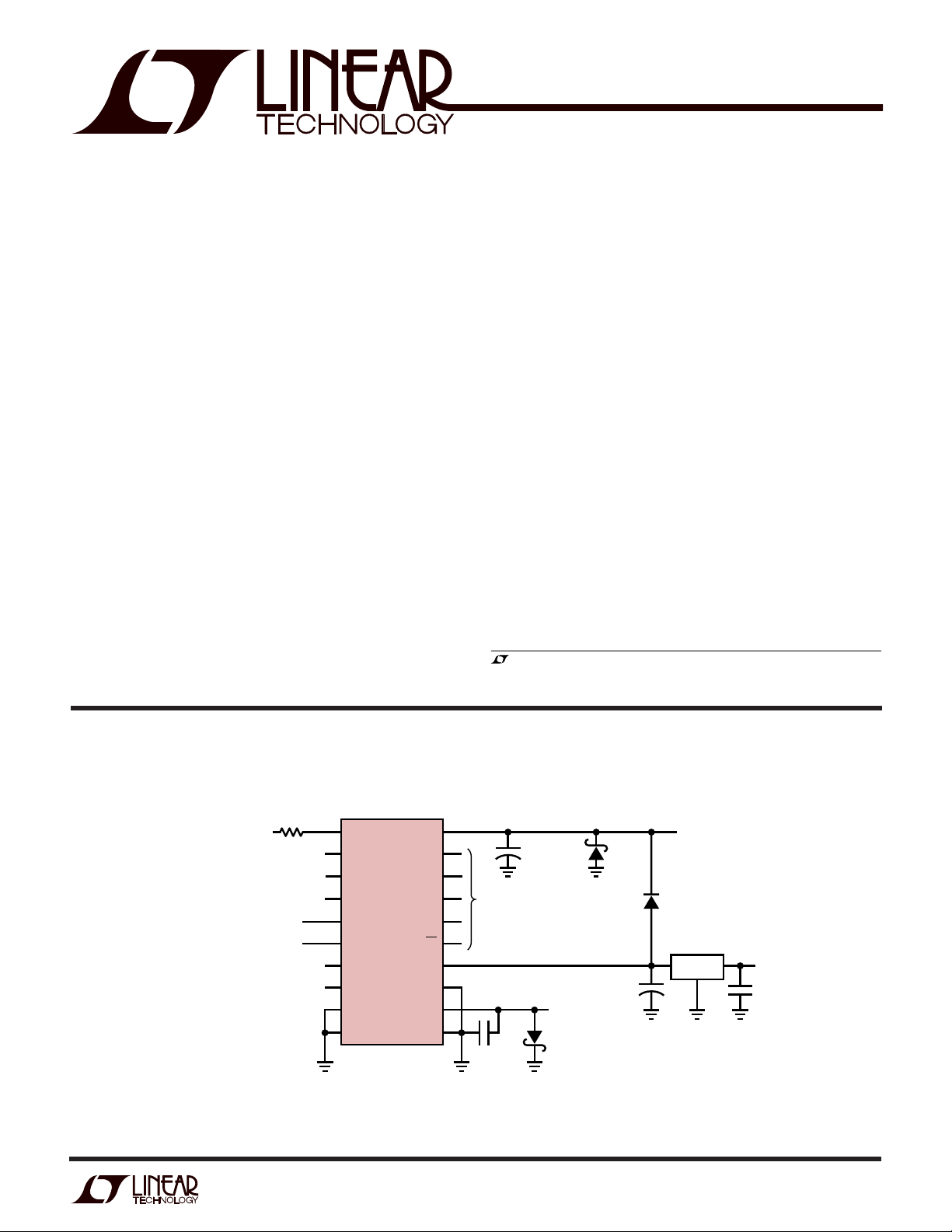
12-Bit 8-Channel Sampling Data Acquisition System
SINGLE-ENDED INPUT
0V TO 5V OR ±5V
±15V OVERVOLTAGE RANGE*
DIFFERENTIAL INPUT (+)
±5V COMMON MODE RANGE (–)
* FOR OVERVOLTAGE PROTECTION ON ONLY ONE CHANNEL LIMIT THE INPUT CURRENT TO 15mA. FOR OVERVOLTAGE PROTECTION
ON MORE THAN ONE CHANNEL LIMIT THE INPUT CURRENT TO 7mA PER CHANNEL AND 28mA FOR ALL CHANNELS. (SEE SECTION ON
OVERVOLTAGE PROTECTION IN THE APPLICATIONS INFORMATION SECTION.) CONVERSION RESULTS ARE NOT VALID WHEN THE SELECTED
OR ANY OTHER CHANNEL IS OVERVOLTAGED (V
1k
CH0
•
•
CH1
•
CH2
CH3
CH4
LTC1290
CH5
•
CH6
•
CH7
•
COM
DGND
V
CC
ACLK
SCLK
D
IN
D
OUT
CS
+
REF
–
REF
–
V
AGND
< V– OR VIN > VCC).
IN
+
22µF
TANTALUM
TO AND FROM
MICROPROCESSOR
0.1µF
1N5817
4.7µF
TANTALUM
–5V
1N5817
5V
1N4148
LT®1027
+
8V TO 40V
1µF
1290 • TA01
1
LTC1290
A
W
O
LUTEXI TIS
S
A
WUW
U
ARB
G
(Notes 1, 2)
Supply Voltage (VCC) to GND or V–........................ 12V
Negative Supply Voltage (V–).................... –6V to GND
Voltage
Analog/Reference Inputs.........(V–) –0.3V to V
CC
+ 0.3V
Digital Inputs........................................ –0.3V to 12V
Digital Outputs ........................... –0.3V to V
CC
+ 0.3V
Power Dissipation............................................. 500mW
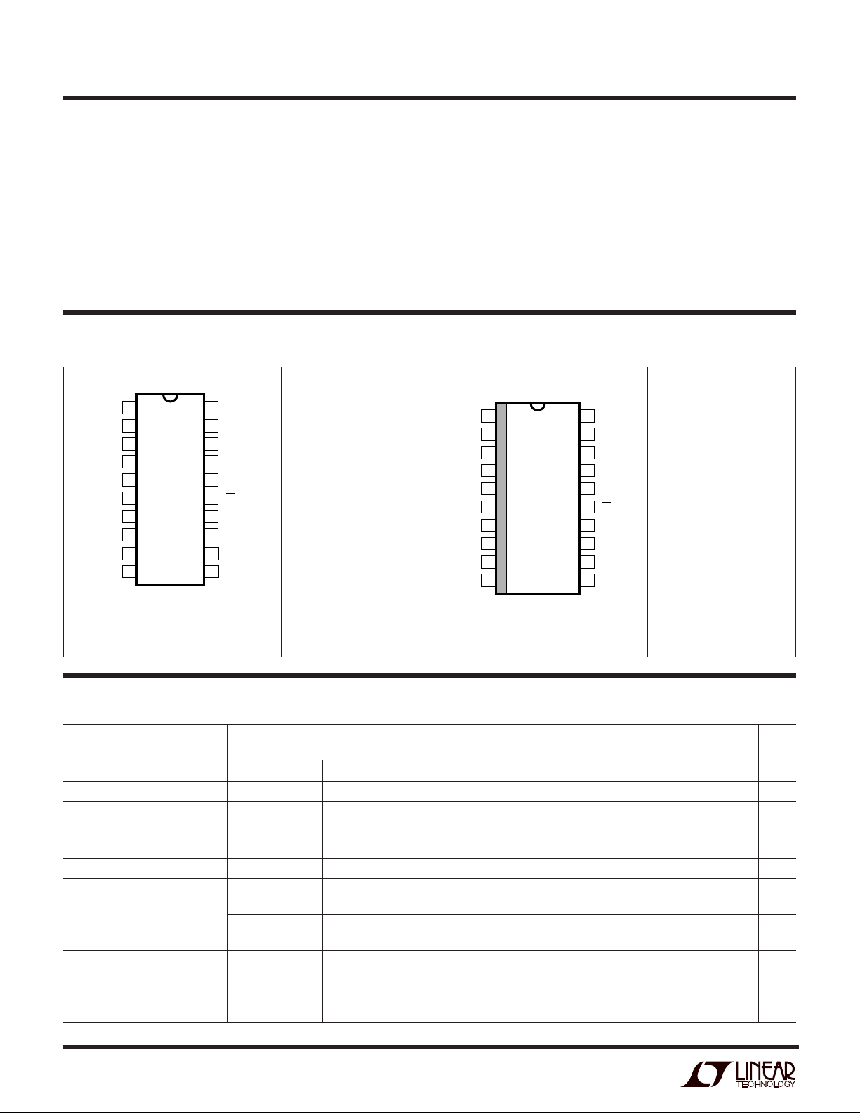
PACKAGE
TOP VIEW
1
CH0
2
CH1
3
CH2
4
CH3
5
CH4
6
CH5
7
CH6
8
CH7
9
COM
10
DGND
J PACKAGE
20-LEAD CERAMIC DIP
T
= 150°C, θJA = 80°C/W (J)
JMAX
T
= 110°C, θJA = 100°C/W (N)
JMAX
/
O
RDER I FOR ATIO
ORDER PART
V
20
CC
ACLK
19
SCLK
18
D
17
IN
D
16
OUT
CS
15
REF
14
REF
13
–
V
12
AGND
11
N PACKAGE
20-LEAD PDIP
+
–
NUMBER
LTC1290BMJ
LTC1290CMJ
LTC1290DMJ
LTC1290BIJ
LTC1290CIJ
LTC1290DIJ
LTC1290BIN
LTC1290CIN
LTC1290DIN
LTC1290BCN
LTC1290CCN
LTC1290DCN
WU
U
Operating Temperature Range
LTC1290BC, LTC1290CC, LTC1290DC.... 0°C to 70°C
LTC1290BI, LTC1290CI, LTC1290DI .... –40°C to 85°C
LTC1290BM, LTC1290CM,
LTC1290DM....................................... –55°C to 125°C
Storage Temperature Range................ –65°C to 150°C
Lead Temperature (Soldering, 10 sec.)................ 300°C
TOP VIEW
1
CH0
2
CH1
3
CH2
4
CH3
5
CH4
6
CH5
7
CH6
8
CH7
9
COM
10
DGND
SW PACKAGE
20-LEAD PLASTIC SO WIDE
= 110°C, θJA = 130°C/W (SW)
T
JMAX
20
V
CC
19
ACLK
18
SCLK
17
D
IN
16
D
OUT
15
CS
+
14
REF
–
13
REF
–
12
V
11
AGND
ORDER PART
NUMBER
LTC1290BCSW
LTC1290CCSW
LTC1290DCSW
LTC1290BISW
LTC1290CISW
LTC1290DISW
UU W
CO VERTER A D ULTIPLEXER CHARACTERISTICS
LTC1290B LTC1290C LTC1290D
PARAMETER CONDITIONS MIN TYP MAX MIN TYP MAX MIN TYP MAX UNITS
Offset Error (Note 4) ● ±1.5 ±1.5 ±1.5 LSB
Linearity Error (INL) (Notes 4,5) ● ±0.5 ±0.5 ±0.75 LSB
Gain Error (Note 4) ● ±0.5 ±1.0 ±4.0 LSB
Minimum Resolution for Which ● 12 12 12 Bits
No Missing Codes are Guaranteed
Analog and REF Input Range (Note 7) (V–) – 0.05V to VCC + 0.05V (V–) – 0.05V to VCC + 0.05V (V–) – 0.05V to VCC + 0.05V V
On Channel Leakage Current On Channel = 5V ● ±1 ±1 ±1 µA
(Note 8) Off Channel = 0V
On Channel = 0V ● ±1 ±1 ±1 µA
Off Channel = 5V
Off Channel Leakage Current On Channel = 5V ● ±1 ±1 ±1 µA
(Note 8) Off Channel = 0V
On Channel = 0V ● ±1 ±1 ±1 µA
Off Channel = 5V
(Note 3)
2
LTC1290
AC CHARACTERISTICS
SYMBOL PARAMETER CONDITIONS MIN TYP MAX UNITS
f
SCLK
f
ACLK
t
ACC
t
SMPL
t
CONV
t
CYC
t
dDO
t
dis
t
en
t
hCS
t
hDI
t
hDO
t
f
t
r
t
suDI
t
suCS
t
WHCS
C
IN
Shift Clock Frequency VCC = 5V (Note 6) 0 2.0 MHz
A/D Clock Frequency VCC = 5V (Note 6) (Note 10) 4.0 MHz
Delay time from CS↓ to D
Analog Input Sample Time See Operating Sequence 7 SCLK
Conversion Time See Operating Sequence 52 ACLK
Total Cycle Time See Operating Sequence (Note 6) 12 SCLK + Cycles
Delay Time, SCLK↓ to D
Delay Time, CS↑ to D
Delay Time, 2nd ACLK↓ to D
Hold Time, CS After Last SCLK↓ VCC = 5V (Note 6) 0 ns
Hold Time, DIN After SCLK↑ VCC = 5V (Note 6) 50 ns
Time Output Data Remains Valid After SCLK↓ 50 ns
D
Fall Time See Test Circuits ● 65 130 ns
OUT
D
Rise Time See Test Circuits ● 25 50 ns
OUT
Setup Time, DIN Stable Before SCLK↑ VCC = 5V (Note 6) 50 ns
Setup Time, CS↓ Before Clocking in (Notes 6, 9) 2 ACLK Cycles
First Address Bit + 100ns
CS High Time During Conversion VCC = 5V (Note 6) 52 ACLK
Input Capacitance Analog Inputs On Channel 100 pF
OUT
OUT
Hi-Z See Test Circuits ● 70 100 ns
OUT
(Note 3)
LTC1290B/LTC1290C/LTC1290D
Data Valid (Note 9) 2 ACLK
56 ACLK
Data Valid See Test Circuits LTC1290BC, LTC1290CC ● 130 220 ns
LTC1290DC, LTC1290BI
LTC1290CI, LTC1290DI
LTC1290BM, LTC1290CM ● 180 270 ns
LTC1290DM
Enabled See Test Circuits ● 130 200 ns
OUT
Analog Inputs Off Channel 5 pF
Digital Inputs 5 pF
Cycles
Cycles
Cycles
Cycles
U
DIGITAL
A
D
DC
LECTRICAL C CHARA TER ST
E
ICS
I
(Note 3)
LTC1290B/LTC1290C/LTC1290D
SYMBOL PARAMETER CONDITIONS MIN TYP MAX UNITS
V
IH
V
IL
I
IH
I
IL
V
OH
V
OL
I
OZ
I
SOURCE
High Level Input Voltage VCC = 5.25V ● 2.0 V
Low Level Input Voltage VCC = 4.75V ● 0.8 V
High Level Input Current VIN = V
Low Level Input Current VIN = 0V ● –2.5 µA
High Level Output Voltage VCC = 4.75V IO = 10µA 4.7 V
Low Level Output Voltage VCC = 4.75V IO = 1.6mA ● 0.4 V
High-Z Output Leakage V
Output Source Current V
CC
= 360µA ● 2.4 4.0 V
I
O
= VCC, CS High ● 3 µA
OUT
V
= 0V, CS High ● –3 µA
OUT
= 0V – 2 0 mA
OUT
● 2.5 µA
3
LTC1290
REFERENCE VOLTAGE, V
REF
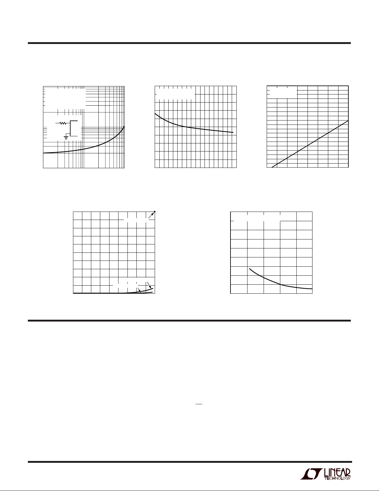
(V)
1
OFFSET ERROR (LSB = • V
REF
)
5
1290 • TPC03
2
3
4
0.9
0.8
0.7
0.6
0.5
0.4
0.3
0.2
0.1
1
4096
VOS = 0.25mV
VOS = 0.125mV
VCC = 5V
U
D
DIGITAL
SYMBOL PARAMETER CONDITIONS MIN TYP MAX UNITS
I
SINK
I
CC
I
REF
–
I
A
Output Sink Current V
Positive Supply Current CS High ● 612 mA
Reference Current V
Negative Supply Current CS High ● 150 µA
DC
LECTRICAL C CHARA TER ST
E
LTC1290B/LTC1290C/LTC1290D
= V
OUT
CC
CS High LTC1290BC, LTC1290CC ● 510 µA
Power Shutdown LTC1290DC, LTC1290BI
ACLK Off LTC1290CI, LTC1290DI
LTC1290BM, LTC1290CM ● 515 µA
LTC1290DM
= 5V ● 10 50 µA
REF
ICS
I
(Note 3)
20 mA
The ● denotes specifications which apply over the full operating
temperature range; all other limits and typicals T
Note 1: Absolute Maximum Ratings are those values beyond which the life
of a device may be impaired.
Note 2: All voltage values are with respect to ground with DGND, AGND
–
and REF
Note 3: V
–5V for bipolar mode, ACLK = 4.0MHz unless otherwise speicfied.
Note 4: These specs apply for both unipolar and bipolar modes. In bipolar
mode, one LSB is equal to the bipolar input span (2V
For example, when V
Note 5: Integral nonlinearity is defined as the deviation of a code from a
straight line passing through the actual endpoints of the transfer curve.
The deviation is measured from the center of the quantization band.
Note 6: Recommended operating conditions.
Note 7: Two on-chip diodes are tied to each reference and analog input
which will conduct for reference or analog input voltages one diode drop
4
wired together (unless otherwise noted).
= 5V, V
CC
26
ACLK = 4MHz
T
A
22
(mA)
18
CC
14
10
SUPPLY CURRENT, I
6
2
46810
+
= 5V, V
REF
= 5V, 1LSB (bipolar) = 2(5V)/4096 = 2.44mV.
REF
LPER
= 25°C
SUPPLY VOLTAGE, VCC (V)
F
= 25°C.
A
–
= 0V, V– = 0V for unipolar mode and
REF
) divided by 4096.
REF
UW
O
R
ATYPICA
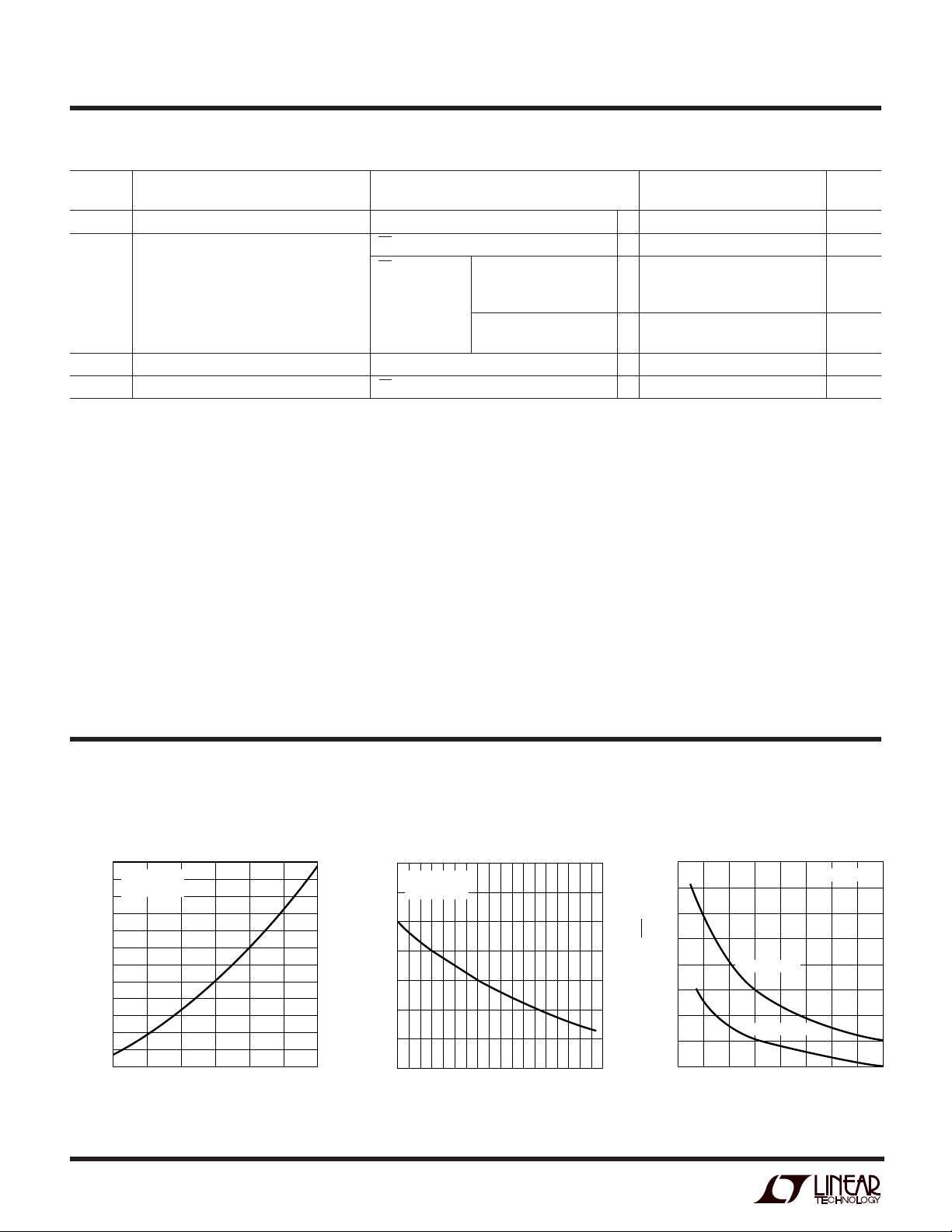
1290 • TPC01
CCHARA TERIST
E
C
(mA)
CC
SUPPLY CURRENT, I
Supply Current vs TemperatureSupply Current vs Supply Voltage
10
ACLK = 4MHz
= 5V
V
9
CC
8
7
6
5
4
3
–50
–10 70
–30
10 90 110 130
AMBIENT TEMPERATURE, TA (°C)
below V– or one diode drop above VCC. Be careful during testing at low
V
levels (4.5V), as high level reference or analog inputs (5V) can cause
CC
this input diode to conduct, especially at elevated temperatures and cause
errors for inputs near full scale. This spec allows 50mV forward bias of
either diode. This means that as long as the reference or analog input does
not exceed the supply voltage by more than 50mV, the output code will be
correct. To achieve an absolute 0V to 5V input voltage range will therefore
require a minimum supply voltage of 4.950V over initial tolerance,
temperature variations and loading.
Note 8: Channel leakage current is measured after the channel selection.
Note 9: To minimize errors caused by noise at the chip select input, the
internal circuitry waits for two ACLK falling edge after a chip select falling
edge is detected before responding to control input signals. Therefore, no
attempt should be made to clock an address in or data out until the
minimum chip select setup time has elapsed.
Note 10: Increased leakage currents at elevated temperatures cause the
S/H to droop, therefore it's recommended that f
≥ 125kHz at 85°C and f
f
ACLK
≥ 15kHz at 25°C.
ACLK
≥ 500kHz at 125°C,
ACLK
ICS
Unadjusted Offset Voltage vs
Reference Voltage
30
50
LT1290 • TPC02

LPER
AMBIENT TEMPERATURE, TA (°C)
–50
MAGNITUDE OF OFFSET CHANGE ∆OFFSET (LSB)
0.5
0.4
0.3
0.2
0.1
0
–10
30
50 130
1290 • TPC06
–30 10
70
90
110
ACLK = 4MHz
V
CC
= 5V
V
REF
= 5V
LTC1290
UW
R
F
O
ATYPICA
CCHARA TERIST
E
C
ICS
Change in Linearity vs Reference
Voltage
1.25
4096
1.00
0.75
0.50
0.25
VCC = 5V
0
0
REFERENCE VOLTAGE, V
1
2
)
REF
1
LINEARITY ERROR (LSB = • V
Change in Linearity Error vs
Temperature
0.6
ACLK = 4MHz
V
0.5
0.4
0.3
0.2
= 5V
CC
= 5V
V
REF
Change in Gain vs Reference
Voltage
0
)
REF
–0.1
1
4096
–0.2
–0.3
–0.4
VCC = 5V
CHANGE IN GAIN ERROR (LSB = • V
–0.5
3
4
5
(V)
REF
1290 • TPC04
1
2
REFERENCE VOLTAGE, V
3
4
REF
5
(V)
1290 • TPC05
Change in Offset vs Temperature
Change in Gain Error vs
Temperature
0.5
ACLK = 4MHz
= 5V
V
CC
= 5V
V
0.4
REF
0.3
0.2
0.1
MAGNITUDE OF LINEARITY CHANGE ∆LINEARITY (LSB)
0
–30 10
–10
–50
AMBIENT TEMPERATURE, TA (°C)
50 130
30
90
110
70
1290 • TPC07
Maximum ACLK Frequency vs
Source Resistance
5
4
3
2
1
MAXIMUM ACLK FREQUENCY* (MHz)
0
100
* MAXIMUM ACLK FREQUENCY REPRESENTS THE ACLK
FREQUENCY AT WHICH A 0.1LSB SHIFT IN THE ERROR AT
ANY CODE TRANSITION FROM ITS 4MHz VALUE IS FIRST DETECTED.
1k 10 k 100k
R
SOURCE
V
R
(Ω)
IN
SOURCE
VCC = 5V
= 5V
V
REF
= 25°C
T
A
+
–
–
INPUT
INPUT
1290 • TPC09
0.1
MAGNITUDE OF GAIN CHANGE ∆GAIN (LSB)
0
–30 10
–50
–10
AMBIENT TEMPERATURE, TA (°C)
30
90
50 130
110
70
1290 • TPC08
Maximum Filter Resistor vs
Cycle Time
10k
1k
** (Ω)
FILTER
100
R
FILTER
V
IN
C
≥ 1µF
10
MAXIMUM R
1.0
10 1000 10000
** MAXIMUM R
AT WHICH A 0.1LSB CHANGE IN FULL-SCALE ERROR FROM
ITS VALUE AT R
FILTER
FILTER
100
CYCLE TIME, t
REPRESENTS THE FILTER RESISTOR VALUE
= 0 IS FIRST DETECTED.
FILTER
CYC
(µs)
+
–
1290 • TPC10
5
LTC1290
REFERENCE VOLTAGE, V
REF
(V)
0
0
PEAK-TO-PEAK NOISE ERROR (LSBs)
0.25
0.75
1.00
1.25
2
4
5
2.25
1290 • TPC15
0.50
13
1.50
1.75
2.00
LTC1290 NOISE 200µV
P-P
LPER
UW
R
F
O
ATYPICA
CCHARA TERIST
E
C
ICS
Sample-and-Hold Acquisition
Time vs Source Resistance
100
V
= 5V
REF
= 5V
V
CC
= 25°C
T
A
0V TO 5V INPUT STEP
R
+
SOURCE
V
IN
10
+
–
S & H AQUISITION TIME TO 0.02% (µs)
1
100
1k 10k
R
+ (Ω)
SOURCE
Input Channel Leakage Current
vs Temperature
1000
900
800
700
600
500
400
300
200
100
INPUT CHANNEL LEAKAGE CURRENT (nA)
0
–30 10
–10
–50
AMBIENT TEMPERATURE, TA (°C)
LTC1290 • TPC11
GUARANTEED
ON CHANNEL
OFF CHANNEL
70 90
50 130
30
Supply Current (Power Shutdown)
vs Temperature
10
ACLK OFF DURING
9
POWER SHUTDOWN
8
(µA)
7
CC
6
5
4
3
SUPPLY CURRENT, I
2
1
0
110
1290 • TPC14
–10
–30 10
–50
AMBIENT TEMPERATURE, TA (°C)
30
50 130
70
Supply Current (Power Shutdown)
vs ACLK
200
VCC = 5V
180
CMOS LEVELS
160
(µA)
140
CC
120
100
80
60
SUPPLY CURRENT, I
40
20
90
110
1290 • TPC12
0
Noise Error vs Reference Voltage
1.00 2.00
ACLK FREQUENCY (MHz)
3.00
4.00
1290 • TPC13
U
PI FU CTIO S
CH0 to CH7 (Pin 1 to Pin 8): Analog Inputs. The analog
inputs must be free of noise with respect to AGND.
COM (Pin 9): Common. The common pin defines the zero
reference point for all single-ended inputs. It must be free
of noise and is usually tied to the analog ground plane.
DGND (Pin 10): Digital Ground. This is the ground for the
internal logic. Tie to the ground plane.
AGND (Pin 11): Analog Ground. AGND should be tied
directly to the analog ground plane.
6
UU
V– (Pin 12): Negative Supply. Tie V– to most negative
potential in the circuit. (Ground in single supply applications.)
REF–, REF+ (Pins 13, 14): Reference Inputs. The reference inputs must be kept free of noise with respect to
AGND.
CS (Pin 15): Chip Select Input. A logic low on this input
enables data transfer.
D
(Pin 16): Digital Data Output. The A/D conversion
OUT
result is shifted out of this output.
LTC1290
D
OUT
3k
100pF
TEST POINT
5V WAVEFORM 2
WAVEFORM 1
LTC1290 • TC02
U
UU
PI FU CTIO S
D
(Pin 17): Digital Data Input. The A/D configuration
IN
word is shifted into this input after CS is recognized.
SCLK (Pin 18): Shift Clock. This clock synchronizes the
serial data transfer.
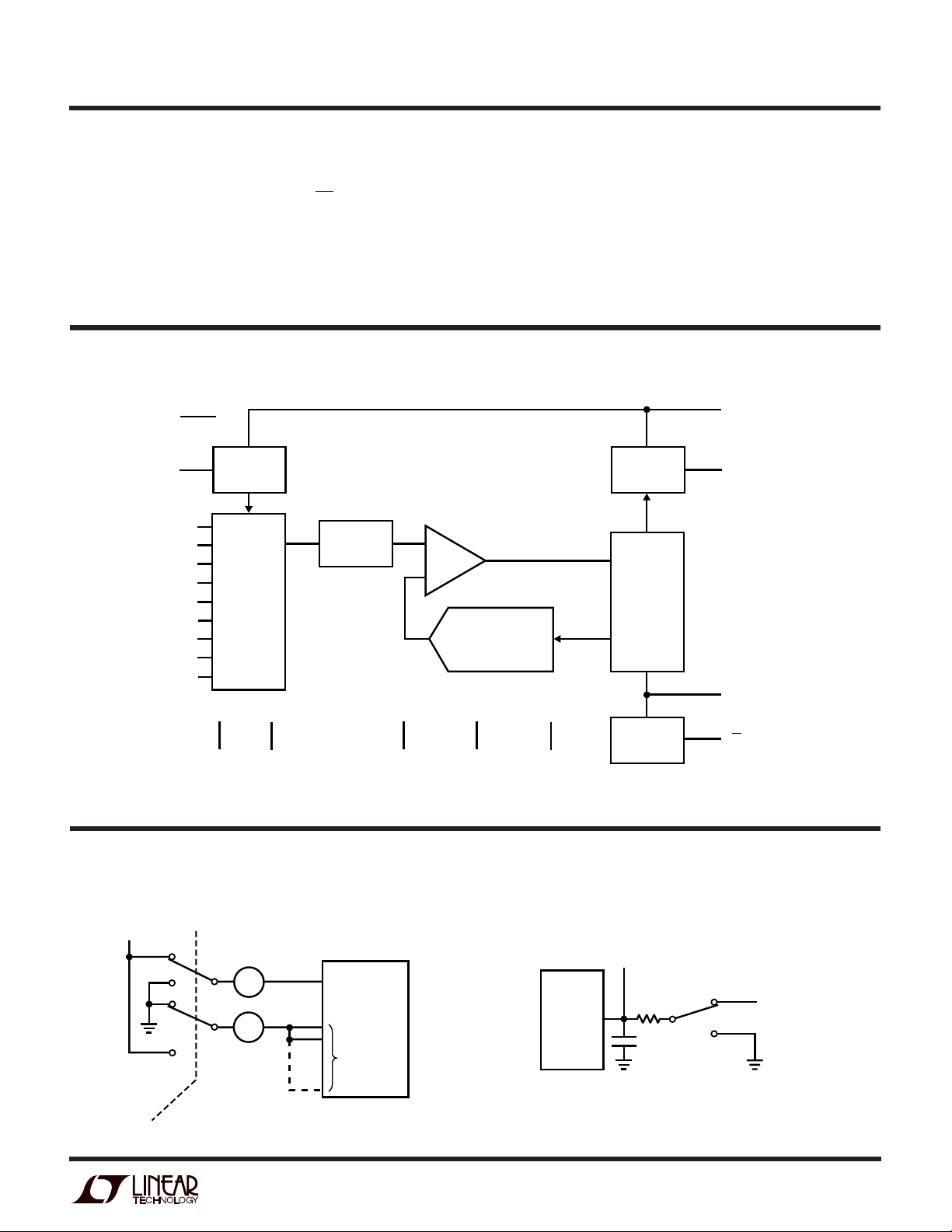
BLOCK DIAGRAM
20
V
CC
1
2
3
4
5
6
7
8
9
INPUT
SHIFT
REGISTER
ANALOG
INPUT MUX
SAMPLE-
AND-
HOLD
COMP
17
D
IN
CH0
CH1
CH2
CH3
CH4
CH5
CH6
CH7
COM
ACLK (Pin 19): A/D Conversion Clock. This clock controls
the A/D conversion process.
VCC (Pin 20): Positive Supply. This supply must be kept
free of noise and ripple by bypassing directly to the analog
ground plane.
18
SCLK
OUTPUT
SHIFT
REGISTER
12-BIT
SAR
12-BIT
CAPACITIVE
DAC
16
D
OUT
19
ACLK
TEST CIRCUITS
5V
10
DGND
11
AGND
On and Off Channel Leakage Current
I
ON
•
•
•
•
ON CHANNEL
OFF
CHANNELS
LTC1290 • TC01
POLARITY
A
I
OFF
A
12
–
V
REF
13
–
REF
14
+
CONTROL
AND
TIMING
Load Circuit for t
15
LTC1290 • BD
and t
dis
CS
en
7
LTC1290
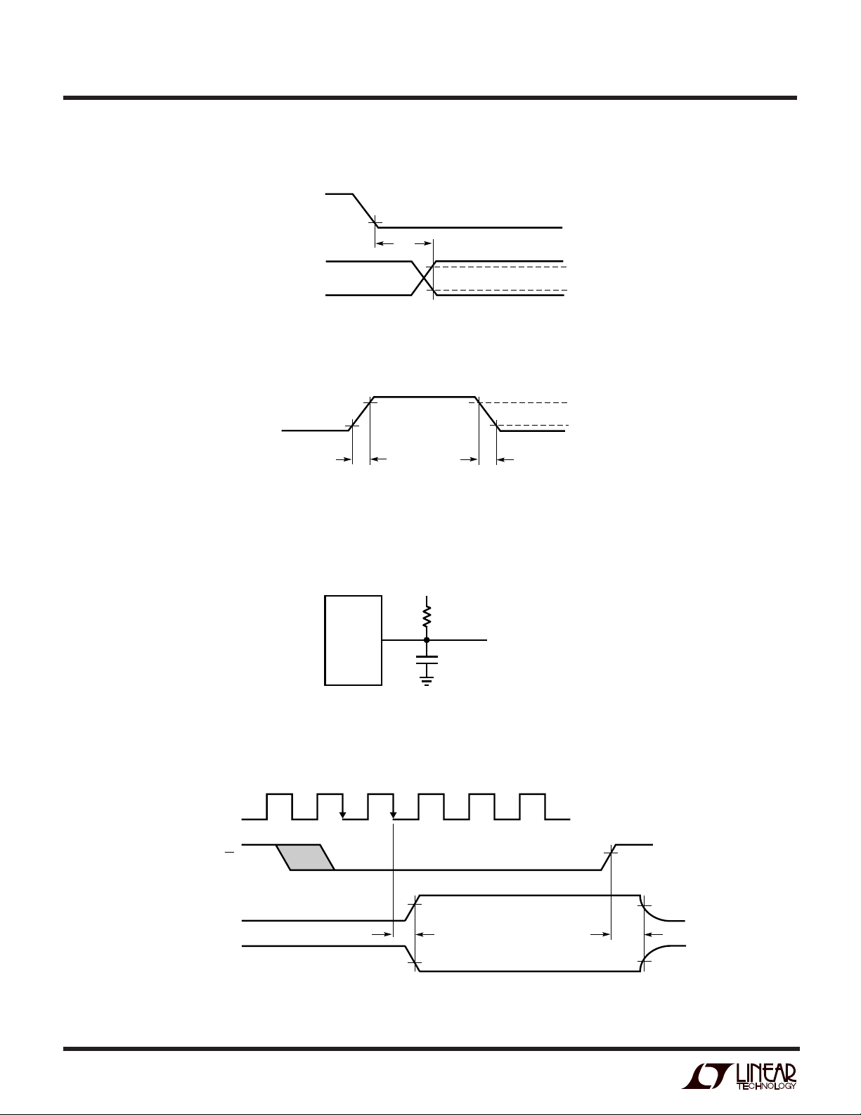
TEST CIRCUITS
Voltage Waveforms for D
SCLK
D
OUT
0.8V
t
Voltage Waveform for D
D
OUT
t
r
Load Circuit for t
Delay Time, t
OUT
dDO
Rise and Fall Times, tr, t
OUT
, tr and t
dDO
dDO
2.4V
0.4V
LTC1290 • TC03
f
2.4V
0.4V
t
LTC1290 • TC04
f
f
1.4V
3k
D
OUT
100pF
Voltage Waveforms for ten and t
ACLK
CS
D
WAVEFORM 1
WAVEFORM 2
NOTE 1: WAVEFORM 1 IS FOR AN OUTPUT WITH INTERNAL CONDITIONS SUCH THAT THE OUTPUT IS HIGH UNLESS DISABLED BY THE OUTPUT CONTROL.
NOTE 2: WAVEFORM 2 IS FOR AN OUTPUT WITH INTERNAL CONDITIONS SUCH THAT THE OUTPUT IS LOW UNLESS DISABLED BY THE OUTPUT CONTROL.
OUT
(SEE NOTE 1)
D
OUT
(SEE NOTE 2)
12
2.4V
t
en
0.8V
TEST POINT
1290 • TC05
dis
2.0V
90%
t
dis
10%
LTC1290 • TC06
8
LTC1290
PPLICATI
A
U
O
S
I FOR ATIO
WU
U
The LTC1290 is a data acquisition component which
contains the following functional blocks:
1. 12-bit successive approximation capacitive A/D
converter
2. Analog multiplexer (MUX)
3. Sample-and-hold (S/H)
4. Synchronous, full duplex serial interface
5. Control and timing logic
DIGITAL CONSIDERATIONS
Serial Interface
The LTC1290 communicates with microprocessors and
other external circuitry via a synchronous, full duplex,
four-wire serial interface (see Operating Sequence). The
shift clock (SCLK) synchronizes the data transfer with
each bit being transmitted on the falling SCLK edge and
captured on the rising SCLK edge in both transmitting and
receiving systems. The data is transmitted and received
simultaneously (full duplex).
Data transfer is initiated by a falling chip select (CS) signal.
After the falling CS is recognized, an 8-bit input word is
shifted into the DIN input which configures the LTC1290
for the next conversion. Simultaneously, the result of the
previous conversion is output on the D
line. At the end
OUT
of the data exchange the requested conversion begins and
CS should be brought high. After t
, the conversion is
CONV
complete and the results will be available on the next data
transfer cycle. As shown below, the result of a conversion
is delayed by one CS cycle from the input word requesting
it.
DIN
D
D
OUTDOUT
WORD 1
IN
WORD 0
DATA
TRANSFER
t
CONV
A/D
CONVERSION
D
WORD 2
IN
D
WORD 1
OUT
DATA
TRANSFER
t
CONVERSION
CONV
A/D
D
IN
D
OUT
WORD 3
WORD 2
LTC1290 • AI01
Input Data Word
The LTC1290 8-bit data word is clocked into the DIN input
on the first eight rising SCLK edges after chip select is
recognized. Further inputs on the DIN pin are then ignored
until the next CS cycle. The eight bits of the input word are
defined as follows:
SGL/
DIFF
SELECT
ODD/
SIGN
MUX ADDRESS
UNIPOLAR/
BIPOLAR
SELECT
1
UNI MSBF WL1
0
MSB-FIRST/
LSB-FIRST
WORD
LENGTH
WL0
LTC1290 • AI02
SCLK
D
D
OUT
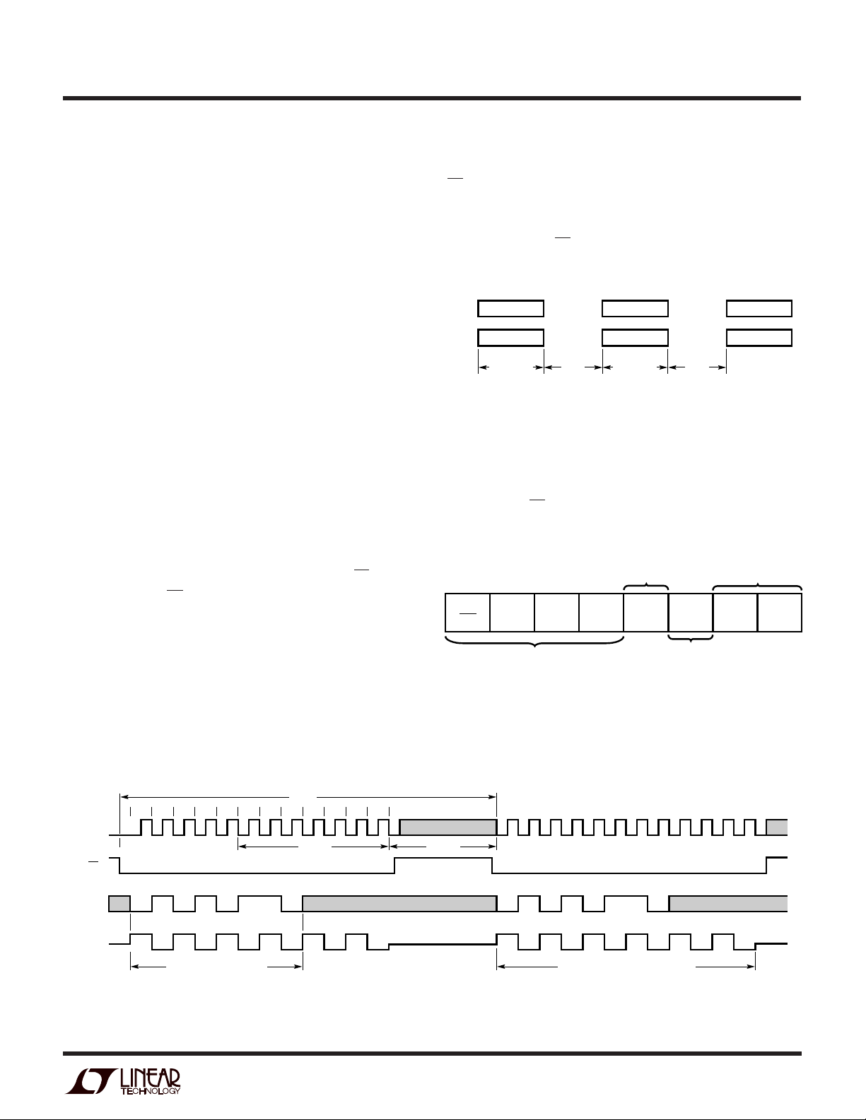
Operating Sequence
(Example: Differential Inputs (CH3-CH2), Bipolar, MSB-First and 12-Bit Word Length)
t
123456789101112
CS
IN
SHIFT CONFIGURATION
WORD IN
CYC
t
SMPL
DON’T CARE
DON’T CARE
t
CONV
B11 B10 B9 B8 B7 B6 B5 B4 B3 B2 B1 B0
(SB)
SHIFT A/D RESULT OUT AND
NEW CONFIGURATION WORD IN
LTC1290 • AI03
9
 Loading...