

Linear Technology LTC1275BCS, LTC1275BCN, LTC1275ACS, LTC1275ACN, LTC1273ACS Datasheet
...
LTC1273
INPUT FREQUENCY (Hz)
10k
0
EFFECTIVE BITS
3
5
7
10
100k 2M
LTC1273/75/76 • TA02
1
4
6
9
12
11
8
2
1M
62
56
74
68
50
S/(N + D) (dB)
f
SAMPLE
= 300kHz
NYQUIST
FREQUENCY
LTC1275/LTC1276
12-Bit, 300ksps Sampling
A/D Converters with Reference
EATU
F
■
Single Supply 5V or ±5V Operation
■
300ksps Sample Rate
■
75mW (Typ) Power Dissipation
■
On-Chip 25ppm/°C Reference
■
Internal Synchronized Clock; No Clock Required
■
High Impedance Analog Input
■
70dB S/(N + D) and 77dB THD at Nyquist
■
±1/2LSB INL and ±3/4LSB DNL Max (A Grade)
■
ESD Protected On All Pins
■
24-Pin Narrow DIP and SOL Packages
■
Variety of Input Ranges:
RE
S
0V to 5V (LTC1273)
±2.5V (LTC1275)
±5V (LTC1276)
U
O
PPLICATI
A
■
High Speed Data Acquisition
■
Digital Signal Processing
■
Multiplexed Data Acquisition Systems
■
Audio and Telecom Processing
■
Spectrum Analysis
S
DUESCRIPTIO
The LTC1273/LTC1275/LTC1276 are 300ksps, sampling
12-bit A/D converters that draw only 75mW from single
5V or ± 5V supplies. These easy-to-use devices come
complete with 600ns sample-and-holds, precision references and internally trimmed clocks. Unipolar and bipolar conversion modes provide flexibility for various applications. They are built with LTBiCMOSTM switched capacitor technology.
These devices have 25ppm/°C (max) internal references.
The LTC1273 converts 0V to 5V unipolar inputs from a
single 5V supply. The LTC1275/LTC1276 convert ±2.5V
and ±5V respectively from ± 5V supplies. Maximum DC
specifications include ±1/2LSB INL, ±3/4LSB DNL and
25ppm/°C full scale drift over temperature. Outstanding
AC performance includes 70dB S/(N + D) and 77dB THD
at the Nyquist input frequency of 150kHz.
The internal clock is trimmed for 2.7µ s maximum conversion time. The clock automatically synchronizes to each
sample command eliminating problems with asynchronous clock noise found in competitive devices. A high
speed parallel interface eases connections to FIFOs, DSPs
and microprocessors.
LTBiCMOSTM is a trademark of Linear Technology Corporation
OUTPUT
U
O
A
PPLICATITYPICAL
Single 5V Supply, 300ksps, 12-Bit Sampling A/D Converter
2.42V
V
REF
+
10µF
PARALLEL BUS
ANALOG INPUT
(0V TO 5V)
0.1µF
8- OR 12-BIT
1
2
3
4
5
6
7
8
9
10
11
12
LTC1273
AIN
V
REF
AGND
D11
D10
D9
D8
D7
D6
D5
D4
DGND
V
NC
BUSY
CS
RD
HBEN
NC
NC
D0/8
D1/9
D2/10
D3/11
24
DD
23
+
22
21
20
19
18
17
16
15
14
13
10µF
µP CONTROL
LINES
LTC1273/75/76 • TA01
Effective Bits and Signal to (Noise + Distortion)
vs Input Frequency
5V
0.1µF
1
LTC1273
LTC1275/LTC1276
A
W
O
LUTEXI T
S
A
WUW
ARB
U
G
I
(Notes 1 and 2)
S
Supply Voltage (VDD).............................................. 12V
Negative Supply Voltage (VSS)
LTC1275/LTC1276.................................. – 6V to GND
Total Supply Voltage (VDD to VSS)
LTC1275/LTC1276............................................... 12V
Analog Input Voltage (Note 3)
LTC1273 .................................... –0.3V to VDD + 0.3V
LTC1275/LTC1276.............. VSS – 0.3V to VDD + 0.3V
Digital Input Voltage (Note 4)
LTC1273 ................................................ –0.3V to 12V
LTC1275/LTC1276......................... VSS – 0.3V to 12V
PACKAGE
A
1
IN
V
2
REF
AGND
3
D11
4
D10
5
D9
6
D8
7
D7
8
D6
9
D5
10
D4
11
DGND
12
N PACKAGE
24-LEAD PLASTIC DIP
T
= 110°C, θJA = 100°C/W (N)
JMAX
= 110°C, θJA = 130°C/W (S)
T
JMAX
/
O
RDER I FOR ATIO
TOP VIEW
VDD
24
NC
23
BUSY
22
CS
21
RD
20
HBEN
19
NC
18
NC
17
D0/8
16
D1/9
15
D2/10
14
D3/11
13
S PACKAGE
24-LEAD PLASTIC SOL
PART NUMBER
LTC1273ACN
LTC1273BCN
LTC1273ACS
LTC1273BCS
(For MIL Grade:
Contact Factory)
WU
ORDER
U
Digital Output Voltage (Note 3)
LTC1273 .................................... –0.3V to VDD + 0.3V
LTC1275/LTC1276.............. VSS – 0.3V to VDD + 0.3V
Power Dissipation............................................. 500mW
Operating Temperature Range
LTC1273AC, LTC1273BC, LTC1275AC
LTC1275BC, LTC1276AC, LTC1276BC .... 0°C to 70°C
Storage Temperature Range ................ –65°C to 150°C
Lead Temperature (Soldering, 10 sec)................. 300°C
TOP VIEW
A
1
IN
V
2
REF
AGND
3
D11
4
D10
5
D9
6
D8
7
D7
8
D6
9
D5
10
D4
11
DGND
12
N PACKAGE
24-LEAD PLASTIC DIP
T
= 110°C, θJA = 100°C/W (N)
JMAX
T
= 110°C, θJA = 130°C/W (S)
JMAX
VDD
24
V
23
SS
BUSY
22
CS
21
RD
20
HBEN
19
NC
18
NC
17
D0/8
16
D1/9
15
D2/10
14
D3/11
13
S PACKAGE
24-LEAD PLASTIC SOL
ORDER
PART NUMBER
LTC1275ACN
LTC1275BCN
LTC1275ACS
LTC1275BCS
LTC1276ACN
LTC1276BCN
LTC1276ACS
LTC1276BCS
(For MIL Grade:
Contact Factory)
U
CO
PARAMETER CONDITIONS MIN TYP MAX MIN TYP MAX UNITS
Resolution (No Missing Codes) ● 12 12 Bits
Integral Linearity Error (Note 7) ±1/2 ±1 LSB
Differential Linearity Error Commercial ● ±3/4 ±1 LSB
Offset Error (Note 8) ±3 ±4 LSB
Full Scale Error ±10 ±15 LSB
Full Scale Tempco I
VERTER
CCHARA TERIST
Commercial
Military
Military
OUT(REFERENCE)
= 0 ● ±5 ±25 ±10 ±45 ppm/°C
With Internal Reference (Notes 5 and 6)
ICS
LTC1273A/LTC1275A/LTC1276A
● ±1/2 ±1 LSB
● ±3/4 ±1 LSB
● ±1 ±1 LSB
● ±4 ±6 LSB
LTC1273B/LTC1275B/LTC1276B
2
LTC1273
LTC1275/LTC1276
W
U
IC
A
DY
SYMBOL PARAMETER CONDITIONS MIN TYP MAX UNITS
S/(N + D) Signal-to-Noise Plus Distortion Ratio 50kHz/150kHz Input Signal 72/70 dB
THD Total Harmonic Distortion 50kHz/150kHz Input Signal –83/–74 dB
Up to 5th Harmonic
Peak Harmonic or Spurious Noise 50kHz/150kHz Input Signal –85/–76 dB
IMD Intermodulation Distortion f
Full Power Bandwidth 4.5 MHz
Full Linear Bandwidth (S/(N + D) ≥ 68dB) 200 kHz
U
IN
IN
IN
ACQ
U
LOG
Analog Input Range (Note 9) 4.95V ≤ VDD ≤ 5.25V (LTC1273) ● 0 to 5 V
Analog Input Leakage Current CS = High ● ±1 µA
Analog Input Capacitance Between Conversions (Sample Mode) 50 pF
Sample-and-Hold Commercial ● 600 ns
Acquisition Time Military ● 1000 ns
UU
A
SYMBOL PARAMETER CONDITIONS MIN TYP MAX UNITS
V
I
C
t
ACCURACY
U
IA
PUT
(Note 5)
(Note 5)
LTC1273A/LTC1275A/LTC1276A
LTC1273B/LTC1275B/LTC1276B
= 29.37kHz, f
IN1
4.75V ≤ V
4.95V ≤ VDD ≤ 5.25V, –5.25V ≤ VSS ≤ –4.95V (LTC1276) ● ±5V
During Conversions (Hold Mode) 5 pF
≤ 5.25V, –5.25V ≤ VSS ≤ –2.45V (LTC1275) ● ±2.5 V
DD
= 32.446kHz –80 dB
IN2
LTC1273A/LTC1275A/LTC1276A
LTC1273B/LTC1275B/LTC1276B
I TER AL REFERE CE CHARACTERISTICS (Note 5)
LTC1273B/LTC1275B/LTC1276BLTC1273A/LTC1275A/LTC1276A
PARAMETER CONDITIONS MIN TYP MAX MIN TYP MAX UNITS
V
Output Voltage I
REF
V
Output Tempco I
REF
V
Line Regulation 4.95V ≤ VDD ≤ 5.25V 0.01 0.01 LSB/V
REF
V
Load Regulation 0V ≤ |I
REF
U
DIGITAL I PUTS A D DIGITAL OUTPUTS
SYMBOL PARAMETER CONDITIONS MIN TYP MAX UNITS
V
IH
V
IL
I
IN
C
IN
V
OH
High Level Input Voltage V
Low Level Input Voltage VDD = 4.95V ● 0.8 V
Digital Input Current VIN = 0V to V
Digital Input Capacitance 5pF
High Level Output Voltage VDD = 4.95V
= 0 2.400 2.420 2.440 2.400 2.420 2.440 V
OUT
= 0 ● ±5 ±25 ±10 ±45 ppm/°C
OUT
–5.25V ≤ V
≤ –4.95V 0.01 0.01 LSB/V
SS
| ≤ 1mA 2 2 LSB/mA
OUT
U
(Note 5)
LTC1273A/LTC1275A/LTC1276A
LTC1273B/LTC1275B/LTC1276B
= 5.25V ● 2.4 V
DD
DD
IO = –10µA 4.7 V
IO = –200µA ● 4.0 V
● ±10 µA
3

LTC1273
LTC1275/LTC1276
U
DIGITAL I PUTS A D DIGITAL OUTPUTS
SYMBOL PARAMETER CONDITIONS MIN TYP MAX UNITS
V
OL
I
OZ
C
OZ
I
SOURCE
I
SINK
Low Level Output Voltage VDD = 4.95V
High Z Output Leakage D11-D0/8 V
High Z Output Capacitance D11-D0/8 CS High (Note 9 ) ● 15 pF
Output Source Current V
Output Sink Current V
POWER REQUIRE E TS
SYMBOL PARAMETER CONDITIONS MIN TYP MAX UNITS
V
DD
V
SS
I
DD
I
SS
P
D
Positive Supply Voltage LTC1273/LTC1276 (Notes 10, 11) 4.95 5.25 V
Negative Supply Voltage LTC1275 (Note 10) –2.45 –5.25 V
Positive Supply Current ● 15 25 mA
Negative Supply Current LTC1275/LTC1276 ● 0.065 0.200 mA
Power Dissipation 75 mW
W
U
TI I G CHARACTERISTICS
U
W
U
(Note 5)
LTC1273A/LTC1275A/LTC1276A
LTC1273B/LTC1275B/LTC1276B
= 160µA 0.05 V
I
O
IO = 1.6mA ● 0.10 0.4 V
= 0V to VDD, CS High ● ±10 µA
OUT
= 0V –10 mA
OUT
OUT
= V
DD
10 mA
(Note 5)
LTC1273A/LTC1275A/LTC1276A
LTC1273B/LTC1275B/LTC1276B
LTC1275 (Note 10) 4.75 5.25 V
LTC1276 (Notes 10, 11) –4.95 –5.25 V
See Timing Characteristics Figures (Note 5)
LTC1273A/LTC1275A/LTC1276A
LTC1273B/LTC1275B/LTC1276B
SYMBOL PARAMETER CONDITIONS MIN TYP MAX UNITS
f
SAMPLE(MAX)
t
CONV
t
1
t
2
t
3
t
4
t
5
t
6
Maximum Sampling Frequency (Note 10)
Commercial ● 300 kHz
Military ● 250 kHz
Conversion Time Commercial ● 2.7 µs
Military ● 3.0 µs
CS to RD Setup Time ● 0ns
RD to BUSY Delay CL = 50pF 80 190 ns
Commercial
Military ● 270 ns
Data Access Time After RD↓ CL = 20pF 40 90 ns
Commercial
Military ● 120 ns
CL = 100pF 50 125 ns
Commercial
Military ● 170 ns
RD Pulse Width ● t
CS to RD Hold Time ● 0ns
Data Setup Time After BUSY↑ 40 70 ns
Commercial
Military ● 100 ns
● 230 ns
● 110 ns
● 150 ns
3
● 90 ns
ns
4
LTC1273
LTC1275/LTC1276
W
U
TI I G CHARACTERISTICS
SYMBOL PARAMETER CONDITIONS MIN TYP MAX UNITS
t
7
t
8
t
9
t
10
t
11
t
12
The
temperature range; all other limits and typicals T
Note 1: Absolute maximum ratings are those values beyond which the life
of a device may be impaired.
Note 2: All voltage values are with respect to ground with DGND and
AGND wired together (unless otherwise noted).
Note 3: When these pin voltages are taken below V
LTC1273) or above V
product can handle input currents greater than 60mA below V
for LTC1273) or above V
Note 4: When these pin voltages are taken below VSS (ground for
LTC1273) they will be clamped by internal diodes. This product can handle
input currents greater than 60mA below V
without latch-up. These pins are not clamped to V
Note 5: VDD = 5V (VSS = –5V for LTC1275/LTC1276), 300kHz at 70°C and
250kHz at 125°C, t
Bus Relinquish Time 20 30 75 ns
HBEN to RD Setup Time ● 0ns
HBEN to RD Hold Time ● 0ns
Delay Between RD Operations ● 40 ns
Delay Between Conversions (Note 10) 500 ns
Aperture Delay of Sample-and-Hold 25 ns
● indicates specifications which apply over the full operating
= 25°C.
A
, they will be clamped by internal diodes. This
DD
without latch-up.
DD
(ground for LTC1273)
SS
DD
= tf = 5ns unless otherwise specified.
r
See Timing Characteristics Figures (Note 5)
LTC1273A/LTC1275A/LTC1276A
LTC1273B/LTC1275B/LTC1276B
Commercial
Military ● 20 90 ns
Commercial
Military ● 1000 ns
Note 6: Linearity, offset and full scale specifications apply for unipolar and
bipolar modes.
Note 7: Integral nonlinearity is defined as the deviation of a code from a
straight line passing through the actual endpoints of the transfer curve.
The deviation is measured from the center of the quantization band.
Note 8: Bipolar offset (LTC1275/LTC1276) is the different voltage
(ground for
SS
(ground
SS
measured from –0.5LSB when the LTC1275/LTC1276 output code flickers
between 0000 0000 0000 and 1111 1111 1111.
Note 9: Guaranteed by design, not subject to test.
Note 10: Recommended operating conditions.
Note11: A
must not exceed VDD or fall below VSS by more than 50mV for
IN
specified accuracy. Therefore the minimum supply voltage for the
LTC1273 is +4.95V. The minimum supplies for the LTC1275 are +4.75V
.
and –2.45V and the minimum supplies for the LTC1276 are ±4.95V.
● 20 85 ns
● 600 ns
W
U
TI I G CHARACTERISTICS
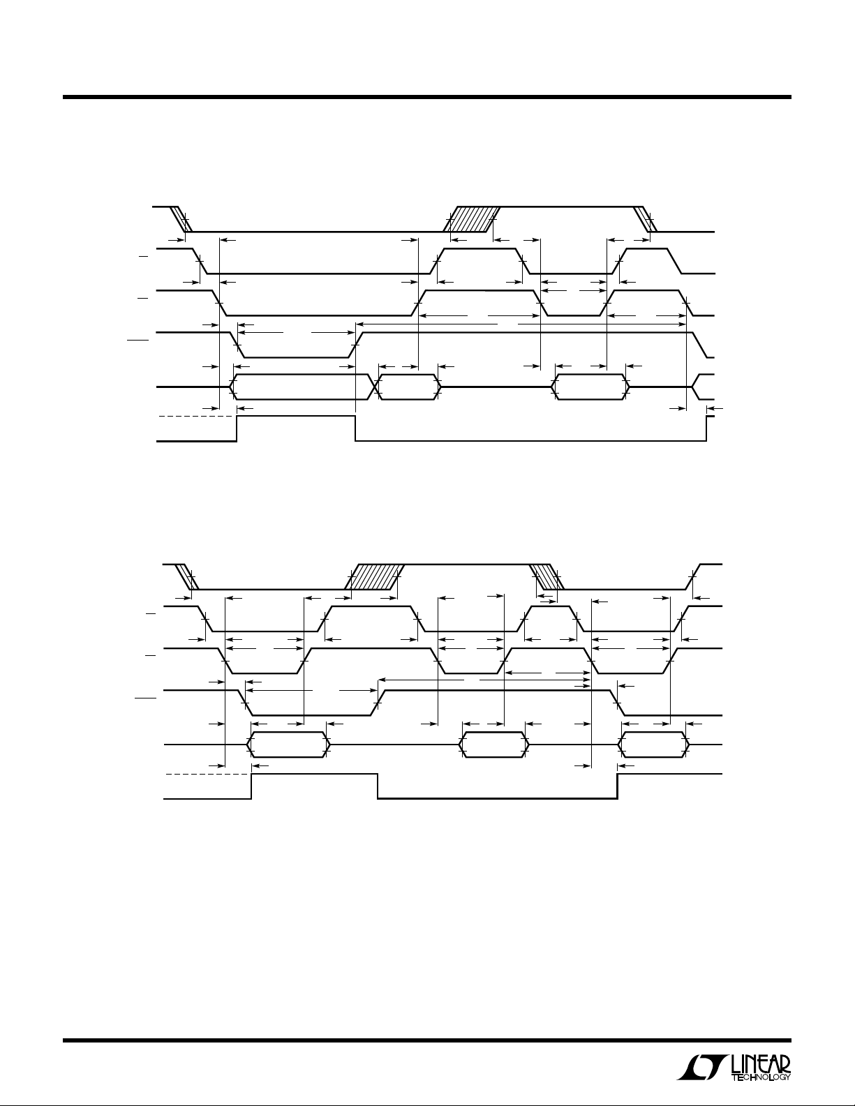
Slow Memory Mode, Parallel Read Timing Diagram
CS
RD
BUSY
DATA
HOLD
TRACK
t
1
t
2
t
CONV
t
3
t
12
OLD DATA
DB11 TO DB0
t
6
t
5
t
7
NEW DATA
DB11 TO DB0
t
11
(Note 5)
t
10
LTC1273/75/76 • TA03
ROM Mode, Parallel Read Timing Diagram
CS
RD
t
1
t
2
t
3
DB11 TO DB0
t
12
t
OLD DATA
t
1
BUSY
DATA
HOLD
TRACK
t
t
CONV
5
t
7
4
t
1
t
11
t
2
t
3
t
12
t
5
t
4
t
CONV
NEW DATA
DB11 TO DB0
t
7
LTC1273/75/76 • TA04
5
LTC1273
LTC1275/LTC1276
W
U
TI I G CHARACTERISTICS
Slow Memory Mode, Two Byte Read Timing Diagram
HBEN
t
8
CS
t
1
RD
t
BUSY
DATA
HOLD
2
t
3
t
12
t
CONV
OLD DATA
DB7 TO DB0
(Note 5)
t
6
NEW DATA
DB7 TO DB0
t
9
t
5
t
7
t
8
t
1
t
4
t
10
t
11
t
3
NEW DATA
DB11 TO DB8
t
9
t
5
t
10
t
7
t
12
TRACK
HBEN
BUSY
DATA
HOLD
TRACK
RD
LTC1273/75/76 • TA05
ROM Mode, Two Byte Read Timing Diagram
t
8
CS
t
1
t
2
t
t
12
3
t
4
OLD DATA
DB7 TO DB0
t
5
t
t
7
t
CONV
9
t
8
t
1
t
4
t
11
t
3
NEW DATA
DB11 TO DB8
t
9
t
5
t
7
t
8
t
1
t
10
t
2
t
t
12
3
t
4
NEW DATA
DB7 TO DB0
t
9
t
5
t
7
LTC1273/75/76 • TA06
6
LPER
RIPPLE FREQUENCY (Hz)
1k
–120
AMPLITUDE OF POWER SUPPLY FEEDTHROUGH (dB)
–40
–20
0
10k 100k 1M
LTC1273/75/76 • TPC08
–60
–80
–100
f
SAMPLE
= 300kHz
V
DD (VRIPPLE
= 1mV)
DGND
(VRIPPLE
= 0.1V)
V
SS (VRIPPLE
= 10mV)
F
O
R
ATYPICA
UW
CCHARA TERIST
E
C
LTC1273
LTC1275/LTC1276
ICS
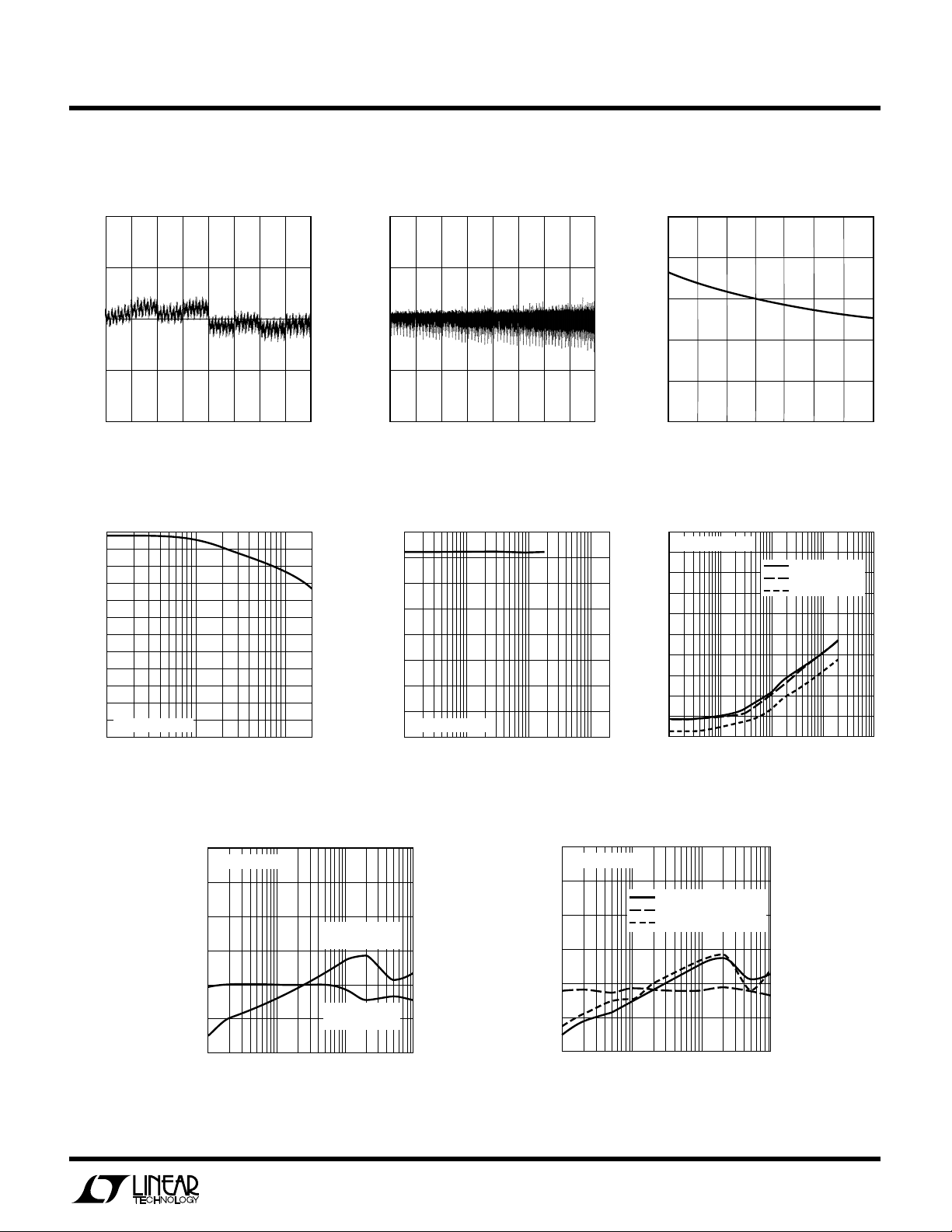
Integral Nonlinearity
1.0
0.5
0
INL ERROR (LSB)
–0.5
–1.0
0
512 1024 1536 2048
ENOBs and S/(N + D)
vs Input Frequency
12
11
10
9
8
7
6
5
4
3
EFFECTIVE NUMBER OF BITS
2
1
f
= 300kHz
SAMPLE
0
10k
100k 2M
INPUT FREQUENCY (Hz)
2560 3072 3584 4096
CODE
LTC1273/75/76 • TPC01
LTC1273/75/76 • TPC04
1M
74
68
62
56
S/(N + D) (dB)
50
Differential Nonlinearity Supply Current vs Temperature
1.0
0.5
0
DNL ERROR (LSB)
–0.5
–1.0
0
512 1024 1536 2048
2560 3072 3584 4096
CODE
LTC1273/75/76 • TPC02
25
20
15
10
SUPPLY CURRENT (mA)
5
0
–50
–25
0
TEMPERATURE (°C)
50
25
Signal-to-Noise Ratio (Without
Harmonics) vs Input Frequency Distortion vs Input Frequency
80
70
60
50
40
30
20
SIGNAL-TO-NOISE RATIO (dB)
10
f
= 300kHz
SAMPLE
0
1k
10k 1M
INPUT FREQUENCY (Hz)
100k
LTC1273/75/76 • TPC05
0
f
= 300kHz
SAMPLE
–10
–20
–30
–40
–50
–60
–70
–80
–90
AMPLITUDE (dB BELOW THE FUNDAMENTAL)
–100
1k 100k 1M 10M
10k
INPUT FREQUENCY (Hz)
THD
2nd HARMONIC
3rd HARMONIC
75
100
LTC1273/75/76 • TPC03
LTC1273/75/76 • TPC06
125
Power Supply Feedthrough
vs Ripple Frequency (LTC1273)
0
f
SAMPLE
–20
–40
–60
–80
–100
–120
1k
AMPLITUDE OF POWER SUPPLY FEEDTHROUGH (dB)
= 300kHz
VDD
= 1mV)
(V
RIPPLE
DGND
= 0.1V)
(V
RIPPLE
10k 100k 1M
RIPPLE FREQUENCY (Hz)
LTC1273/75/76 • TPC07
Power Supply Feedthrough
vs Ripple Frequency (LTC1275/76)
7
LTC1273
LTC1275/LTC1276
LPER
F
O
R
ATYPICA
UW
CCHARA TERIST
E
C
ICS
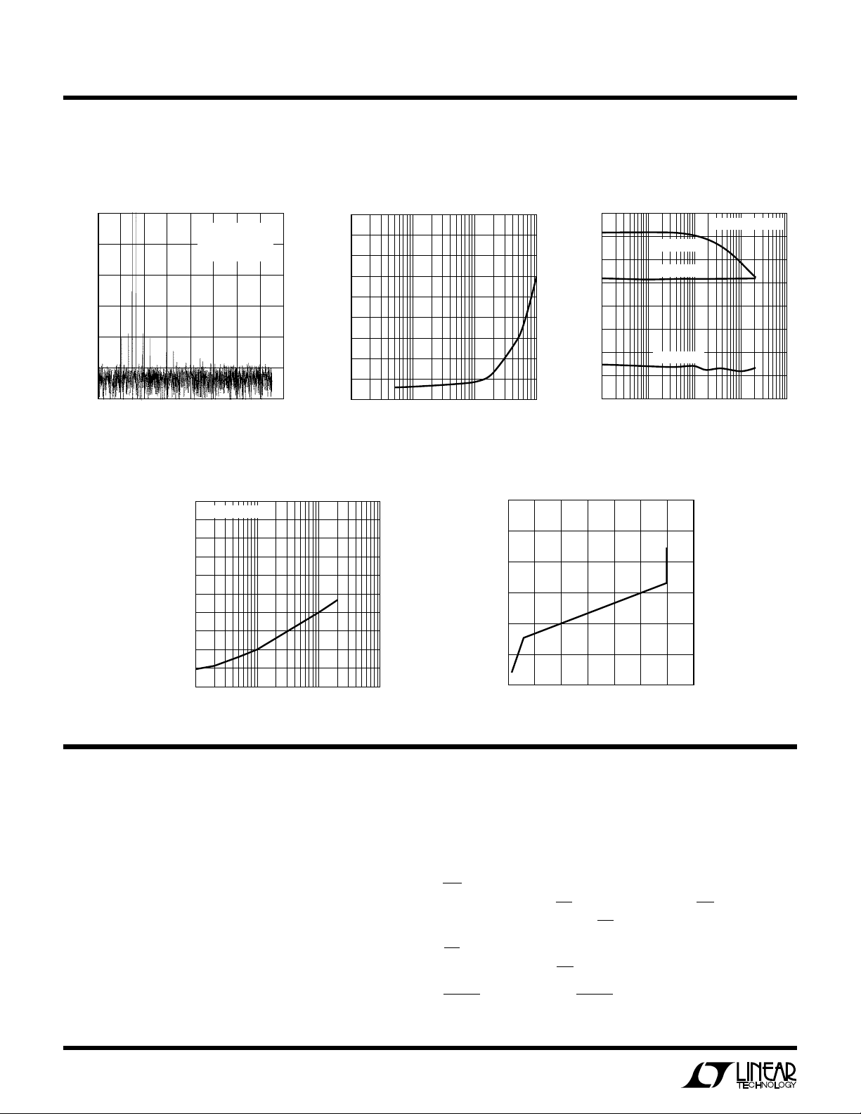
Intermodulation Distortion Plot
0
f
SAMPLE
f
–20
–40
–60
AMPLITUDE (dB)
–80
–100
–120
20 60 100
0
40 80
FREQUENCY (kHz)
IN1
f
IN2
Spurious Free Dynamic Range
vs Input Frequency
0
f
SAMPLE
–10
–20
–30
–40
–50
–60
–70
–80
–90
SPURIOUS FREE DYNAMIC RANGE (dB)
–100
10k
= 300kHz
= 29.37kHz
= 32.446kHz
120
140
160
LTC1273/75/76 • F05
= 300kHz
100k 1M 10M
INPUT FREQUENCY (Hz)
Acquisition Time
vs Source Impedance
4500
4000
3500
3000
2500
2000
1500
ACQUISITION TIME (ns)
1000
500
0
10
LTC1273/75/76 • TPC12
100 1k 10k
R
(Ω)
SOURCE
LTC1273/75/76 • TPC10
Reference Voltage
vs Load Current
2.435
2.430
2.425
2.420
2.415
REFERENCE VOLTAGE (V)
2.410
2.405
–4 –2 –1 2
–5
S/(N + D) vs Input Frequency and
Amplitude
80
70
60
50
40
30
20
10
SIGNAL/(NOISE + DISTORTION) (dB)
0
1k
–3 0 1
LOAD CURRENT (mA)
VIN = 0dB
VIN = –20dB
VIN = –60dB
10k 100k 10M
INPUT FREQUENCY (Hz)
LTC1273/75/76 • TPC13
f
SAMPLE
LTC1273/75/76 • TPC11
= 300kHz
1M
UU U
PI FU CTIO S
A
(Pin 1): Analog Input. 0V to 5V (LTC1273), ± 2.5V
IN
(LTC1275) or ±5V (LTC1276).
V
(Pin 2): +2.42V Reference Output. Bypass to AGND
REF
(10µ F tantalum in parallel with 0.1µF ceramic).
AGND (Pin 3): Analog Ground.
D11-D4 (Pins 4 to 11): Three-State Data Outputs.
DGND (Pin 12): Digital Ground.
D3/11-D0/8 (Pins 13 to 16): Three-State Data Outputs.
NC (Pins 17 and 18): No Connection.
8
HBEN (Pin 19): High Byte Enable Input. This pin is used to
multiplex the internal 12-bit conversion result into the
lower bit outputs (D7-D0/8). See Table 1. HBEN also
disables conversion start when HIGH.
RD (Pin 20): READ Input. This active low signal starts a
conversion when CS and HBEN are low. RD also enables
the output drivers when CS is low.
CS (Pin 21): The CHIP SELECT Input must be low for the
ADC to recognize RD and HBEN inputs.
BUSY (Pin 22): The BUSY Output shows the converter
status. It is low when a conversion is in progress.
 Loading...