

Linear Technology LTC1098LIS8, LTC1098LCS8, LTC1098IS8, LTC1096LCS8, LTC1096IN8 Datasheet
...
LTC1096/LTC1096L
SAMPLE FREQUENCY, f
SMPL
(kHz)
0.1
1
SUPPLY CURRENT, I
CC
(µA)
10
100
1000
1 10 100
LTC1096/98 • TPC03
TA = 25°C
V
CC
= V
REF
= 5V
LTC1098/LTC1098L
Micropower Sampling
8-Bit Serial I/O A/D Converters
EATU
F
■
80µA Maximum Supply Current
■
1nA Typical Supply Current in Shutdown
■
8-Pin SO Plastic Package
■
5V Operation (LTC1096/LTC1098)
■
3V Operation (LTC1096L/LTC1098L)(2.65V Min)
■
Sample-and-Hold
■
16µs Conversion Time
■
33kHz Sample Rate
■
±0.5LSB Total Unadjusted Error Over Temp
■
Direct 3-Wire Interface to Most MPU Serial Ports and
RE
S
All MPU Parallel I/O Ports
U
O
PPLICATI
A
■
Battery-Operated Systems
■
Remote Data Acquisition
■
Battery Monitoring
■
Battery Gas Gauges
■
Temperature Measurement
■
Isolated Data Acquisition
, LTC and LT are registered trademarks of Linear Technology Corporation.
S
DUESCRIPTIO
The LTC®1096/LTC1096L/LTC1098/LTC1098L are
micropower, 8-bit A/D converters that draw only 80µ A of
supply current when converting. They automatically power
down to 1nA typical supply current whenever they are not
performing conversions. They are packaged in 8-pin SO
packages and have both 3V (L) and 5V versions. These
8-bit, switched-capacitor, successive approximation ADCs
include sample-and-hold. The LTC1096/LTC1096L have a
single differential analog input. The LTC1098/LTC1098L
offer a software selectable 2-channel MUX.
On-chip serial ports allow efficient data transfer to a wide
range of microprocessors and microcontrollers over three
wires. This, coupled with micropower consumption, makes
remote location possible and facilitates transmitting data
through isolation barriers.
These circuits can be used in ratiometric applications or
with an external reference. The high impedance analog
inputs and the ability to operate with reduced spans
(below 1V full scale) allow direct connection to sensors
and transducers in many applications, eliminating the
need for gain stages.
ANALOG INPUT
0V TO 5V RANGE
U
O
A
PPLICATITYPICAL
10µW, S8 Package, 8-Bit A/D
Samples at 200Hz and Runs Off a 5V Battery
5V1µF
CS/
SHUTDOWN
+IN
–IN
GND
LTC1096
V
CC
CLK
D
OUT
V
REF
MPU
(e.g., 8051)
P1.4
P1.3
P1.2
LTC1096/8 • TA01
Supply Current vs Sample Rate
1
LTC1096/LTC1096L
LTC1098/LTC1098L
A
W
O
LUTEXI T
S
A
WUW
ARB
U
G
I
S
(Notes 1 and 2)
Supply Voltage (VCC) to GND................................... 12V
Voltage
Analog and Reference ................ –0.3V to V
CC
+ 0.3V
Digital Inputs......................................... –0.3V to 12V
Digital Outputs ........................... –0.3V to V
CC
+ 0.3V
Power Dissipation.............................................. 500mW
Storage Temperature Range ................. –65°C to 150°C
WU
/
PACKAGE
CS/
SHUTDOWN
1096
1096A
+IN
–IN
GND
N8 PACKAGE
8-LEAD PLASTIC DIP
T
JMAX
T
JMAX
S8 PART MARKING
O
RDER I FOR ATIO
TOP VIEW
1
2
3
4
8-LEAD PLASTIC SOIC
= 150°C, θJA = 130°C/W (N8)
= 150°C, θJA = 175°C/W (S8)
1096I
1096IA
V
8
CLK
7
D
6
V
5
S8 PACKAGE
1096L
1096LI
CC
OUT
REF
ORDER PART
NUMBER
LTC1096ACN8
LTC1096ACS8
LTC1096AIN8
LTC1096AIS8
LTC1096CN8
LTC1096CS8
LTC1096IN8
LTC1096IS8
LTC1096LCS8
LTC1096LIS8
Operating Temperature
LTC1096AC/LTC1096C/LTC1096LC/
LTC1098AC/LTC1098C/LTC1098LC ....... 0°C to 70°C
LTC1096AI/LTC1096I/LTC1096LI/
LTC1098AI/LTC1098I/LTC1098LI ..... –40°C to 85°C
Lead Temperature (Soldering, 10 sec.)................ 300°C
U
(Notes 3)
TOP VIEW
CS/
SHUTDOWN
8-LEAD PLASTIC DIP
1
2
CH0
3
CH1
4
GND
N8 PACKAGE
T
= 150°C, θJA = 130°C/W (N8)
JMAX
= 150°C, θJA = 175°C/W (S8)
T
JMAX
S8 PART MARKING
1098
1098A
1098I
1098IA
V
8
CC(VREF)
CLK
7
D
6
OUT
D
5
IN
S8 PACKAGE
8-LEAD PLASTIC SOIC
1098L
1098LI
ORDER PART
LTC1098ACN8
LTC1098ACS8
LTC1098AIN8
LTC1098AIS8
LTC1098CN8
LTC1098CS8
LTC1098IN8
LTC1098IS8
LTC1098LCS8
LTC1098LIS8
NUMBER
Consult factory for Military grade parts.
WUW
UUU
RECO E DED OPERATI G CO DITIO S
LTC1096/LTC1098
SYMBOL PARAMETER CONDITIONS MIN TYP MAX UNITS
V
CC
VCC = 5V Operation
f
CLK
t
CYC
t
hDI
t
suCS
t
WAKEUP
t
suDI
t
WHCLK
Supply Voltage LTC1096 3.0 9 V
Clock Frequency VCC = 5V 25 500 kHz
Total Cycle Time LTC1096, f
Hold Time, DIN After CLK↑ VCC = 5V 150 ns
Setup Time CS↓ Before First CLK↑ (See Operating Sequence) VCC = 5V, LTC1096 500 ns
Wake-Up Time CS↓ Before First CLK↓ After First CLK↑ VCC = 5V, LTC1096 10 µs
(See Figure 1 LTC1096 Operating Sequence)
Wake-Up Time CS↓ Before MSBF Bit CLK↓ VCC = 5V, LTC1098 10 µs
(See Figure 2 LTC1098 Operating Sequence)
Setup Time, DIN Stable Before CLK↑ VCC = 5V 400 ns
CLK High Time VCC = 5V 0.8 µs
LTC1098 3.0 6 V
= 500kHz 29 µs
LTC1098, f
VCC = 5V, LTC1098 500 ns
CLK
= 500kHz 29 µs
CLK
2
LTC1096/LTC1096L
LTC1098/LTC1098L
WUW
UUU
RECO E DED OPERATI G CO DITIO S
LTC1096/LTC1098
SYMBOL PARAMETER CONDITIONS MIN TYP MAX UNITS
t
WLCLK
t
WHCS
t
WLCS
VCC = 3V Operation
f
CLK
t
CYC
t
hDI
t
suCS
t
WAKEUP
t
suDI
t
WHCLK
t
WLCLK
t
WHCS
t
WLCS
CLK Low Time VCC = 5V 0.8 µs
CS High Time Between Data Transfer Cycles VCC = 5V 1 µs
CS Low Time During Data Transfer LTC1096, f
LTC1098, f
Clock Frequency VCC = 3V 25 250 kHz
Total Cycle Time LTC1096, f
LTC1098, f
Hold Time, DIN After CLK↑ VCC = 3V 450 ns
Setup Time CS↓ Before First CLK↑ (See Operating Sequence) VCC = 3V, LTC1096 1 µs
VCC = 3V, LTC1098 1 µs
Wake-Up Time CS↓ Before First CLK↓ After First CLK↑ VCC = 3V, LTC1096 10 µs
(See Figure 1 LTC1096 Operating Sequence)
Wake-Up Time CS↓ Before MSBF Bit CLK↓ VCC = 3V, LTC1098 10 µs
(See Figure 2 LTC1098 Operating Sequence)
Setup Time, DIN Stable Before CLK↑ VCC = 3V 1 µs
CLK High Time VCC = 3V 1.6 µs
CLK Low Time VCC = 3V 1.6 µs
CS High Time Between Data Transfer Cycles VCC = 3V 2 µs
CS Low Time During Data Transfer LTC1096, f
LTC1098, f
= 500kHz 28 µs
CLK
= 500kHz 28 µs
CLK
= 250kHz 58 µs
CLK
= 250kHz 58 µs
CLK
= 250kHz 56 µs
CLK
= 250kHz 56 µs
CLK
LTC1096L/LTC1098L
SYMBOL PARAMETER CONDITIONS MIN TYP MAX UNITS
V
CC
f
CLK
t
CYC
t
hDI
t
suCS
t
WAKEUP
t
suDI
t
WHCLK
t
WLCLK
t
WHCS
t
WLCS
Supply Voltage 2.65 4.0 V
Clock Frequency VCC = 2.65V 25 250 kHz
Total Cycle Time LTC1096L, f
Hold Time, DIN After CLK↑ VCC = 2.65V 450 ns
Setup Time CS↓ Before First CLK↑ (See Operating Sequence) VCC = 2.65V, LTC1096L 1 µs
Wake-Up Time CS↓ Before First CLK↓ After First CLK↑ VCC = 2.65V, LTC1096L 10 µs
(See Figure 1, LTC1096L Operating Sequence)
Wake-Up Time CS↓ Before MSBF Bit CLK↓ VCC = 2.65V, LTC1098L 10 µs
(See Figure 2, LTC1098L Operating Sequence)
Setup Time, DIN Stable Before CLK↑ VCC = 2.65V 1 µs
CLK High Time VCC = 2.65V 1.6 µs
CLK Low Time VCC = 2.65V 1.6 µs
CS High Time Between Data Transfer Cycles VCC = 2.65V 2 µs
CS Low Time During Data Transfer LTC1096L, f
LTC1098L, f
V
= 2.65V, LTC1098L 1 µs
CC
LTC1098L, f
= 250kHz 58 µs
CLK
= 250kHz 58 µs
CLK
= 250kHz 56 µs
CLK
= 250kHz 56 µs
CLK
3
LTC1096/LTC1096L
LTC1098/LTC1098L
UU W
CO VERTER A D ULTIPLEXER CHARACTERISTICS
LTC1096/LTC1098
VCC = 5V, V
PARAMETER CONDITIONS MIN TYP MAX MIN TYP MAX UNITS
Resolution (No Missing Code) ● 8 8 Bits
Offset Error ● ±0.5 ±0.5 LSB
Linearity Error (Note 4) ● ±0.5 ±0.5 LSB
Full Scale Error ● ±0.5 ±1.0 LSB
Total Unadjusted Error (Note 5) V
Analog Input Range (Notes 6, 7) V
REF Input Range (Notes 6, 7) 4.5 ≤ VCC ≤ 6V V
Analog Input Leakage Current (Note 8) ● ±1.0 ±1.0 µA
LTC1096/LTC1098
VCC = 3V, V
PARAMETER CONDITIONS MIN TYP MAX MIN TYP MAX UNITS
Resolution (No Missing Code) ● 8 8 Bits
Offset Error ● ±0.75 ±1.0 LSB
Linearity Error (Notes 4, 9) ● ±0.5 ±1.0 LSB
Full-Scale Error ● ±1.0 ±1.0 LSB
Total Unadjusted Error
Analog Input Range (Notes 6, 7) V
REF Input Range (Notes 6, 7, 9) 3V ≤ VCC ≤ 6V V
Analog Input Leakage Current (
= 5V, f
REF
= 2.5V, f
REF
= 500kHz, unless otherwise noted.
CLK
= 5.000V ● ±0.5 ±1.0 LSB
REF
6V < VCC ≤ 9V, LTC1096 V
= 250kHz, unless otherwise noted.
CLK
(Notes 5, 9)
V
= 2.500V ● ±1.0 ±1.5 LSB
REF
Notes 8, 9
)
LTC1096A/LTC1098A
–0.05V to VCC + 0.05V
–0.05V to V
–0.05V to 6V
–0.05V to VCC + 0.05V
–0.05V to V
● ±1.0 ±1.0 µ A
LTC1096/LTC1098
+ 0.05V
CC
LTC1096/LTC1098LTC1096A/LTC1098A
+ 0.05V
CC
LTC1096L/LTC1098L
VCC = 2.65V, V
PARAMETER CONDITIONS MIN TYP MAX UNITS
Resolution (No Missing Code) ● 8 Bits
Offset Error ● ±1.0 LSB
Linearity Error (Note 4) ● ±1.0 LSB
Full-Scale Error ● ±1.0 LSB
Total Unadjusted Error
Analog Input Range (Notes 6, 7) –0.05V to VCC + 0.05V V
REF Input Range (Note 6) 2.65V ≤ VCC ≤ 4.0V –0.05V to VCC + 0.05V V
Analog Input Leakage Current (Note 8) ● ±1.0 µA
= 2.5V, f
REF
(Notes 5)
= 250kHz, unless otherwise noted.
CLK
V
= 2.5V ● ±1.5 LSB
REF
LTC1096L/LTC1098L
4
LTC1096/LTC1096L
LTC1098/LTC1098L
U
DIGITAL AND DC ELECTRICAL CHARACTERISTICS
LTC1096/LTC1098
VCC = 5V, V
SYMBOL PARAMETER CONDITIONS MIN TYP MAX UNITS
V
IH
V
IL
I
IH
I
IL
V
OH
V
OL
I
OZ
I
SOURCE
I
SINK
I
REF
I
CC
= 5V, unless otherwise noted.
REF
High Level Input Voltage VCC = 5.25V ● 2.0 V
Low Level Input Voltage VCC = 4.75V ● 0.8 V
High Level Input Current VIN = V
CC
● 2.5 µA
Low Level Input Current VIN = 0V ● –2.5 µA
High Level Output Voltage VCC = 4.75V, IO = 10µA ● 4.5 4.74 V
VCC = 4.75V, IO = 360µA ● 2.4 4.72 V
Low Level Output Voltage VCC = 4.75V, IO = 1.6mA ● 0.4 V
Hi-Z Output Leakage CS ≥ V
Output Source Current V
Output Sink Current V
= 0V –25 mA
OUT
= V
OUT
Reference Current CS = V
≥ 200µs, f
t
CYC
t
= 29µs, f
CYC
Supply Current CS = V
LTC1096, t
LTC1096, t
LTC1098, t
LTC1098, t
IH
CC
CC
CC
≤ 50kHz ● 3.500 7.5 µA
CLK
= 500kHz ● 35.000 50.0 µA
CLK
≥ 200µs, f
CYC
= 29µs, f
CYC
≥ 200µs, f
CYC
= 29µs, f
CYC
≤ 50kHz ● 40 80 µA
CLK
= 500kHz ● 120 180 µA
CLK
≤ 50kHz ● 44 88 µA
CLK
= 500kHz ● 155 230 µA
CLK
● ±3.0 µA
45 mA
● 0.001 2.5 µA
● 0.001 3.0 µA
LTC1096/LTC1098
VCC = 3V, V
SYMBOL PARAMETER CONDITIONS MIN TYP MAX UNITS
V
IH
V
IL
I
IH
I
IL
V
OH
V
OL
I
OZ
I
SOURCE
I
SINK
I
REF
I
CC
= 2.5V, unless otherwise noted.
REF
High Level Input Voltage VCC = 3.6V ● 1.9 V
Low Level Input Voltage VCC = 3V ● 0.45 V
High Level Input Current (Note 9) VIN = V
CC
● 2.5 µA
Low Level Input Current (Note 9) VIN = 0V ● –2.5 µA
High Level Output Voltage VCC = 3V, IO = 10µA ● 2.3 2.69 V
VCC = 3V, IO = 360µA ● 2.1 2.64 V
Low Level Output Voltage VCC = 3V, IO = 400µA ● 0.3 V
Hi-Z Output Leakage (Note 9) CS ≥ V
Output Source Current (Note 9) V
Output Sink Current (Note 9) V
= 0V –10 mA
OUT
= V
OUT
Reference Current (Note 9) CS = V
t
≥ 200µs, f
CYC
= 58µs, f
t
CYC
Supply Current (Note 9) CS = V
LTC1096, t
LTC1096, t
LTC1098, t
LTC1098, t
IH
CC
CC
CC
≤ 50kHz ● 3.500 7.5 µA
CLK
= 250kHz ● 35.000 50.0 µA
CLK
≥ 200µs, f
CYC
= 58µs, f
CYC
≥ 200µs, f
CYC
= 58µs, f
CYC
≤ 50kHz ● 40 80 µA
CLK
= 250kHz ● 120 180 µA
CLK
≤ 50kHz ● 44 88 µA
CLK
= 250kHz ● 155 230 µA
CLK
● ±3.0 µA
15 mA
● 0.001 2.5 µA
● 0.001 3.0 µA
5
LTC1096/LTC1096L
LTC1098/LTC1098L
U
DIGITAL AND DC ELECTRICAL CHARACTERISTICS
LTC1096L/LTC1098L
VCC = 2.65V, V
SYMBOL PARAMETER CONDITIONS MIN TYP MAX UNITS
V
IH
V
IL
I
IH
I
IL
V
OH
V
OL
I
OZ
I
SOURCE
I
SINK
I
REF
I
CC
= 2.5V, f
REF
= 250kHz, unless otherwise noted.
CLK
High Level Input Voltage VCC = 3.6V ● 1.9 V
Low Level Input Voltage VCC = 2.65V ● 0.45 V
High Level Input Current VIN = V
CC
● 2.5 µA
Low Level Input Current VIN = 0V ● –2.5 µA
High Level Output Voltage VCC = 2.65V, IO = 10µA ● 2.3 2.64 V
= 2.65V, IO = 360µA ● 2.1 2.50 V
V
CC
Low Level Output Voltage VCC = 2.65V, IO = 400µA ● 0.3 V
Hi-Z Output Leakage CS = High ● ±3.0 µA
Output Source Current V
Output Sink Current V
Reference Current CS = V
Supply Current CS = V
= 0V –10 mA
OUT
= V
OUT
CC
CC
≥ 200µs, f
t
CYC
= 58µs, f
t
CYC
CC
LTC1096L, t
LTC1096L, t
LTC1098L, t
LTC1098L, t
● 0.001 2.5 µA
≤ 50kHz ● 3.500 7.5 µA
CLK
= 250kHz ● 35.000 50.0 µ A
CLK
● 0.001 3.0 µA
≥ 200µs, f
CYC
= 58µs, f
CYC
≥ 200µs, f
CYC
= 58µs, f
CYC
≤ 50kHz ● 40 80 µA
CLK
= 250kHz ● 120 180 µA
CLK
≤ 50kHz ● 44 88 µA
CLK
= 250kHz ● 155 230 µA
CLK
15 mA
AC CHARACTERISTICS
LTC1096/LTC1098
VCC = 5V, V
SYMBOL PARAMETER CONDITIONS MIN TYP MAX UNITS
t
SMPL
f
SMPL
(MAX)
t
CONV
t
dDO
t
dis
t
en
t
hDO
t
f
t
r
C
IN
REF
= 5V, f
= 500kHz, unless otherwise noted.
CLK
Analog Input Sample Time See Operating Sequence 1.5 CLK Cycles
Maximum Sampling Frequency ● 33 kHz
Conversion Time See Operating Sequence 8 CLK Cycles
Delay Time, CLK↓ to D
Delay Time, CS↑ to D
Delay Time, CLK↓ to D
Time Output Data Remains Valid After CLK↓ C
D
Fall Time See Test Circuits ● 70 250 ns
OUT
D
Rise Time See Test Circuits ● 25 100 ns
OUT
Data Valid See Test Circuits ● 200 450 ns
OUT
Hi-Z See Test Circuits ● 170 450 ns
OUT
Enable See Test Circuits ● 60 250 ns
OUT
= 100pF 180 ns
LOAD
Input Capacitance Analog Inputs On Channel 25 pF
Analog Inputs Off Channel 5 pF
Digital Input 5 pF
6
LTC1096/LTC1096L
LTC1098/LTC1098L
AC CHARACTERISTICS
LTC1096/LTC1098
VCC = 3V, V
SYMBOL PARAMETER CONDITIONS MIN TYP MAX UNITS
t
SMPL
f
SMPL(MAX)
t
CONV
t
dDO
t
dis
t
en
t
hDO
t
f
t
r
C
IN
= 2.5V, f
REF
= 250kHz, unless otherwise noted.
CLK
Analog Input Sample Time See Operating Sequence 1.5 CLK Cycles
Maximum Sampling Frequency ● 16.5 kHz
Conversion Time See Operating Sequence 8 CLK Cycles
Delay Time, CLK↓ to D
Delay Time, CS↑ to D
Delay Time, CLK↓ to D
Time Output Data Remains Valid After CLK↓ C
D
Fall Time See Test Circuits (Note 9) ● 70 250 ns
OUT
D
Rise Time See Test Circuits (Note 9) ● 50 150 ns
OUT
Data Valid See Test Circuits (Note 9) ● 500 1000 ns
OUT
Hi-Z See Test Circuits (Note 9) ● 220 800 ns
OUT
Enable See Test Circuits (Note 9) ● 160 480 ns
OUT
= 100pF 400 ns
LOAD
Input Capacitance Analog Inputs On Channel 25 pF
Analog Inputs Off Channel 5 pF
Digital Input 5 pF
LTC1096L/LTC1098L
VCC = 2.65V, V
SYMBOL PARAMETER CONDITIONS MIN TYP MAX UNITS
t
SMPL
f
SMPL(MAX)
t
CONV
t
dDO
t
dis
t
en
t
hDO
t
f
t
r
C
IN
The ● denotes specifications which apply over the operating temperature
range.
Note 1: Absolute Maximum Ratings are those values beyond which the life
of a device may be impaired.
Note 2: All voltage values are with respect to GND.
Note 3: For the 8-lead PDIP, consult the factory.
Note 4: Linearity error is specified between the actual and points of the
A/D transfer curve.
Note 5: Total unadjusted error includes offset, full scale, linearity,
multiplexer and hold step errors.
Note 6: Two on-chip diodes are tied to each reference and analog input
which will conduct for reference or analog input voltages one diode drop
below GND or one diode drop above V
bias of either diode. This means that as long as the reference or analog
= 2.5V, f
REF
= 250kHz, unless otherwise noted.
CLK
Analog Input Sample Time See Operating Sequence 1.5 CLK Cycles
Maximum Sampling Frequency ● 16.5 kHz
Conversion Time See Operating Sequence 8 CLK Cycles
Delay Time, CLK↓ to D
Delay Time, CS↑ to D
Delay Time, CLK↓ to D
Time Output Data Remains Valid After CLK↓ C
D
Fall Time See Test Circuits ● 70 250 ns
OUT
D
Rise Time See Test Circuits ● 50 200 ns
OUT
Data Valid See Test Circuits ● 500 1000 ns
OUT
Hi-Z See Test Circuits ● 220 800 ns
OUT
Enable See Test Circuits ● 160 480 ns
OUT
= 100pF 400 ns
LOAD
Input Capacitance Analog Inputs On Channel 25 pF
Analog Inputs Off Channel 5 pF
Digital Input 5 pF
input does not exceed the supply voltage by more than 50mV, the output
code will be correct. To achieve an absolute 0V to 5V input voltage range
will therefore require a minimum supply voltage of 4.950V over initial
tolerance, temperature variations and loading. For 5.5V < V
CC
≤ 9V,
reference and analog input range cannot exceed 5.55V. If reference and
analog input range are greater than 5.55V, the output code will not be
guaranteed to be correct.
Note 7: The supply voltage range for the LTC1096L/LTC1098L is from
2.65V to 4V. The supply voltage range for the LTC1096 is from 3V to 9V,
but the supply voltage range for the LTC1098 is only from 3V to 6V.
Note 8: Channel leakage current is measured after the channel selection.
Note 9: These specifications are either correlated from 5V specifications or
. This spec allows 50mV forward
CC
guaranteed by design.
7
LTC1096/LTC1096L
REFERENCE VOLTAGE (V)
0
CHANGE IN LINEARITY (LSB)
0
0.25
4
LTC1096/98 • TPC06
–0.25
–O.50
1
2
3
5
0.50
TA = 25°C
V
CC
= 5V
F
CLK
= 500kHz
VOLTAGE REFERENCE (V)
0
CHANGE IN GAIN (LSB)
0
0.25
4
LTC1096/98 • TPC09
–0.25
–O.50
1
2
3
5
0.50
TA = 25°C
V
CC
= 5V
F
CLK
= 500kHz
LTC1098/LTC1098L
LPER
F
O
R
ATYPICA
UW
CCHARA TERIST
E
C
ICS
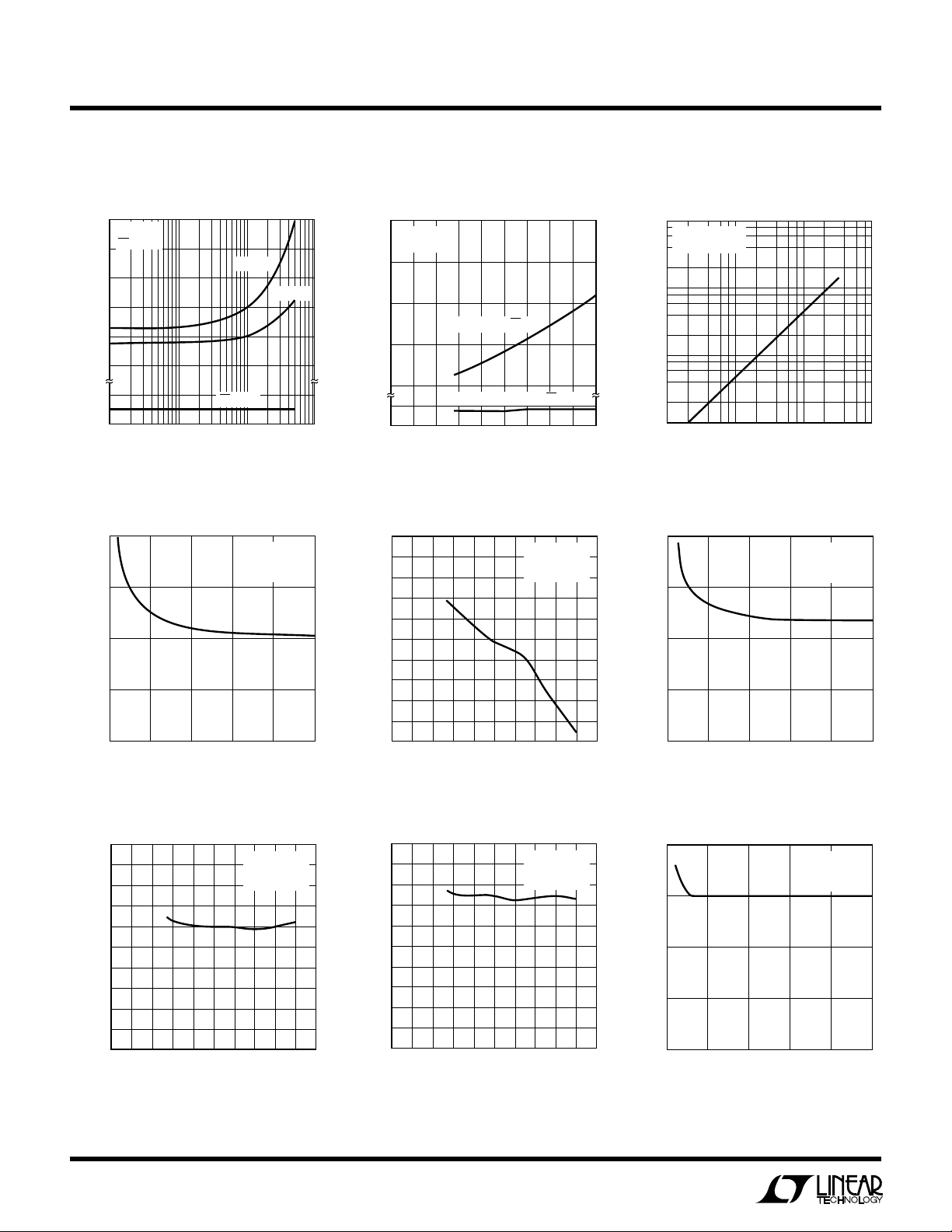
Supply Current vs Clock Rate
for Active and Shutdown Modes
250
TA = 25°C
CS = 0V
200
150
(µA)
CC
100
50
10
SUPPLY CURRENT, I
0.002
0
1
CS = V
10 100 1000
FREQUENCY (kHz)
Change in Offset vs
Reference Voltage LTC1096
)
REF
0.50
0.25
0
–0.25
–0.50
MAGNITUDE OF OFFSET CHANGE (LSB = 1/256 × V
1
0
2
REFERENCE VOLTAGE (V)
Change in Linearity vs
Supply Voltage
0.5
0.4
0.3
0.2
0.1
0
–0.1
–0.2
CHANGE IN LINEARTY (LSB)
–0.3
–0.4
–0.5
19
0
3
2
SUPPLY VOLTAGE, VCC (V)
5
4
100
VCC = 9V
(µA)
VCC = 5V
CC
LTC1096/98 • TPC01
TA = 25°C
= 5V
V
CC
= 500kHz
F
CLK
3
4
5
LTC1096/98 • TPC04
T
= 25°C
A
= 2.5V
V
REF
= 100kHz
F
CLK
7
6
8
10
LTC1096/98 • TPC07
CC
SUPPLY CURRENT, I
0.001
–0.1
–0.2
–0.3
–0.4
MAGNITUDE OF OFFSET CHANGE (LSB)
–0.5
–0.1
–0.2
CHANGE IN GAIN (LSB)
–0.3
–0.4
–0.5
Supply Current vs Supply Voltage
Active and Shutdown Modes
T
= 25°C
A
V
REF
80
60
40
20
0
13
0
= 2.5V
“ACTIVE” MODE CS = 0
“SHUTDOWN” MODE CS = V
2
SUPPLY VOLTAGE,VCC (V)
59
4
7
6
LTC1096/98 • TPC02
CC
8
1000
(µA)
100
CC
SUPPLY CURRENT, I
Change in Offset vs
Supply Voltage
0.5
0.4
0.3
0.2
0.1
0
3
2
19
0
4
SUPPLY VOLTAGE, VCC (V)
T
= 25°C
A
= 2.5V
V
REF
= 100kHz
F
CLK
7
6
8
5
LTC1096/98 • TPC05
10
Change in Gain vs Supply Voltage
0.5
0.4
0.3
0.2
0.1
0
3
2
19
0
4
SUPPLY VOLTAGE, VCC (V)
T
= 25°C
A
= 2.5V
V
REF
= 100kHz
F
CLK
7
6
8
5
10
LTC1096/98 • TPC08
Supply Current vs Sample
Frequency LTC1096
TA = 25°C
= V
V
10
1
0.1
= 5V
CC
REF
1 10 100
SAMPLE FREQUENCY, f
SMPL
Change in Linearity vs
Reference Voltage LTC1096
Change in Gain vs
Reference Voltage LTC1096
(kHz)
LTC1096/98 • TPC03
8
TEMPERATURE (°C)
–60
LEAKAGE CURRENT (nA)
10
100
1000
100
LTC1096/98 • TPC15
1
0.1
0.01
–20
20
60
140
–40 0
40
80 120
V
REF
= 5V
V
CC
= 5V
ON CHANNEL
OFF CHANNEL
FREQUENCY (kHz)
0
–100
AMPLITUDE (dB)
–90
–70
–60
–50
0
–30
2
4
LTC1096/98 • TPC18
–80
–20
–10
–40
6
8
10 12
14 16
TA = 25°C
V
CC
= V
REF
= 5V
f
SMPL
= 31.25kHz
f
IN
= 5.8kHz
LPER
F
O
R
ATYPICA
UW
CCHARA TERIST
E
C
LTC1096/LTC1096L
LTC1098/LTC1098L
ICS
Maximum Clock Frequency vs
Source Resistance
1
TA = 25°C
= V
V
0.75
0.50
0.25
MAXIMUM CLOCK FREQUENCY* (MHz)
0
1
= 5V
CC
REF
R
SOURCE
V
IN
10 100
–
(kΩ)
Wake-Up Time vs Supply Voltage
4
TA = 25°C
= 2.5V
V
REF
3
+ INPUT
– INPUT
–
R
SOURCE
LTC1096/98 • TPC10
Maximum Clock Frequency vs
Supply Voltage
1.5
TA = 25°C
= 2.5V
V
REF
1.25
1.0
0.75
0.5
0.25
MAXIMUM CLOCK FREQUENCY (MHz)
0
0
2468
SUPPLY VOLTAGE (V)
Minimum Wake-Up Time
vs Source Resistance
10
TA = 25°C
= 5V
V
REF
7.5
LTC1096/98 • TPC11
Digital Input Logic Threshold
vs Supply Voltage
5
TA = 25°C
4
3
2
LOGIC THRESH0LD (V)
1
10
0
2
0
SUPPLY VOLTAGE, VCC (V)
6
8
4
10
LTC1096/98 • TPC12
Input Channel Leakage Current
vs Temperature
2
WAKE-UP TIME (µs)
1
0
0
Minimum Clock Frequency for
0.1LSB Error† vs Temperature
200
180
160
140
120
100
80
60
40
MINIMUM CLOCK FREQUENCY (kHz)
20
0
–60
* Maximum CLK frequency represents the clock frequency at which a 0.1LSB shift in the error at any code
transition from its 0.75MHz value is first detected.
†
As the CLK frequency is decreased from 500kHz, minimum CLK frequency (∆error ≤ 0.1LSB) represents
the frequency at which a 0.1LSB shift in any code transition from its 500kHz value is first detected.
2
SUPPLY VOLTAGE, VCC (V)
V
= 5V
REF
= 5V
V
CC
–20
–40 0
20
TEMPERATURE (°C)
4
40
6
60
80 120
8
LTC1096/98 • TPC13
100
•
10
140
5.0
2.5
MINIMUM WAKE-UP TIME (µs)
0
1
ENOBs vs Frequency
10
9
8
7
6
5
ENOBs
4
3
2
TA = 25°C
= V
V
CC
1
f
SMPL
REF
= 31.25kHz
1
0
V
10 100
R
(kΩ)
SOURCE
= 5V
10 100
FREQUENCY (kHz)
R
SOURCE
IN
LTC1096/98 • TPC17
+
+
–
LTC1096/98 • TPC14
FFT Plot
9
 Loading...