

Linear Technology LTC1098LCS8, LTC1098L, LTC1096LAIS8, LTC1096LACS8, LTC1096LIS8 Datasheet
...
Final Electrical Specifications
SAMPLE FREQUENCY (kHz)
0.1
1
SUPPLY CURRENT, I
CC
(µA)
10
100
1000
1 10 100
1096/8 TA02
LTC1096L/LTC1098L
Low Voltage, Micropower
Sampling 8-Bit Serial I/O
A/D Converters
December 1995
EATU
F
■
Specified at 2.65V Minimum Supply
■
Maximum Supply Current: 80µA
■
Auto Shutdown to 1nA
■
8-Pin SO Package
■
On-Chip Sample-and-Hold
■
Conversion Time: 32µs
■
Sample Rates: 16.5ksps
■
I/O Compatible with SPI, MICROWIRETM, etc.
PPLICATI
A
■
Battery-Operated Systems
■
Remote Data Acquisition
■
Isolated Data Acquisition
■
Battery Monitoring
■
Temperature Measurement
RE
S
O
U
S
DUESCRIPTIO
The LTC®1096L/LTC1098L are 3V micropower, 8-bit successive approximation sampling A/D converters. They
typically draw only 40µ A of supply current when converting and automatically power down to a typical supply
current of 1nA between conversions. They are packaged in
8-pin SO packages and operate on a 3V supply. These 8bit, switched capacitor, successive approximation ADCs
include a sample-and-hold. The LTC1096L has a single
differential analog input. The LTC1098L offers a software
selectable 2-channel multiplexed input.
On-chip serial ports allow efficient data transfer to a wide
range of microprocessors and microcontrollers over three
wires. This, coupled with micropower consumption, makes
remote location possible and facilitates transmitting data
through isolation barriers.
The circuits can be used in ratiometric applications or with
an external reference. The high impedance analog inputs
and the ability to operate with reduced spans (to 1V full
scale) allow direct connection to sensors and transducers
in many applications, eliminating the need for gain stages.
, LTC and LT are registered trademarks of Linear Technology Corporation.
MICROWIRE is a registered trademark of National Semiconductor Corporation.
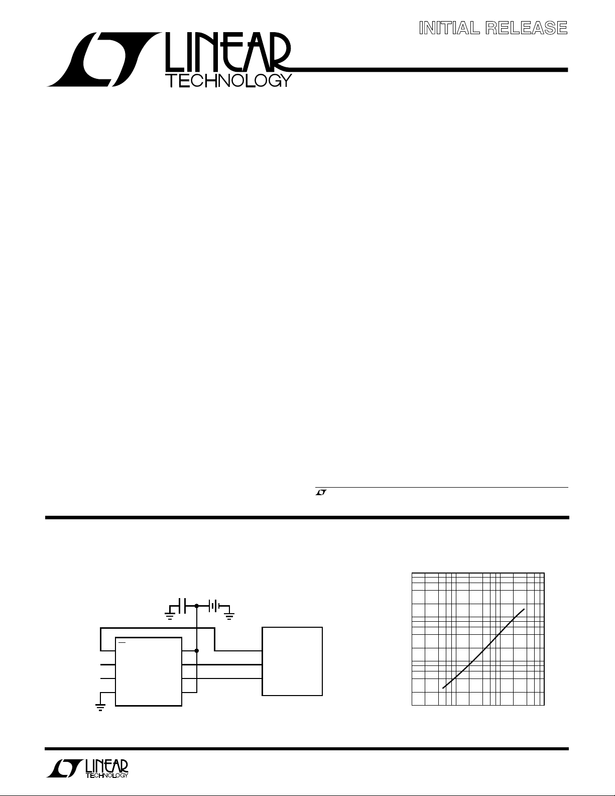
ANALOG INPUT
0V TO 3V RANGE
A
PPLICATITYPICAL
Samples at 200Hz and Runs Off a 3V Battery
1
CS/
SHDN
2
+IN
LTC1096L
3
–IN
4
GND
U
O
Supply Current vs Sample Rate10µW, SO-8 Package, 8-Bit A/D Converter
3V1µF
8
V
CC
7
CLK
6
D
OUT
V
REF
SERIAL DATA LINK
5
Information furnished by Linear Technology Corporation is believed to be accurate and reliable.
However, no responsibility is assumed for its use. Linear Technology Corporation makes no representation that the interconnection of its circuits as described herein will not infringe on existing patent rights.
MPU
SERIAL DATA LINK
(MICROWIRE AND
SPI COMPATIBLE)
1096/8 TA01
1
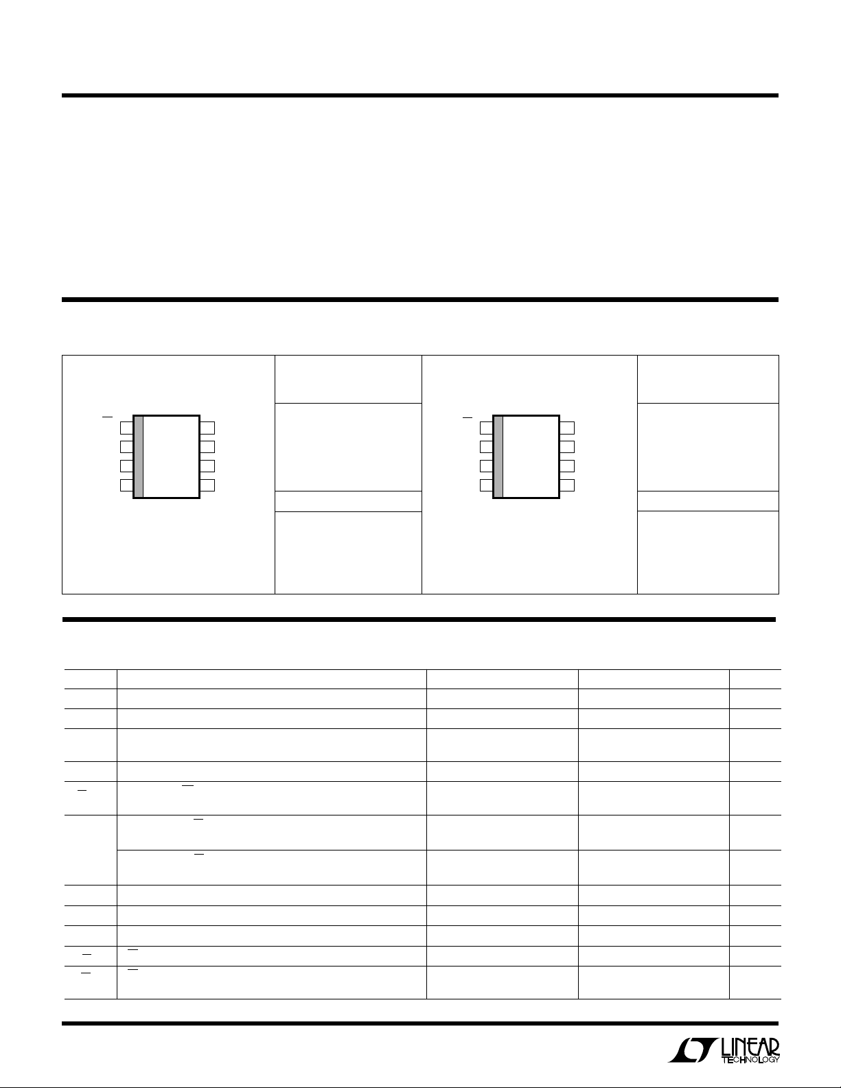
LTC1096L/LTC1098L
TOP VIEW
+IN
–IN
GND
V
CC
CLK
D
OUT
V
REF
S8 PACKAGE
8-LEAD PLASTIC SO
CS/
SHDN
1
2
3
4
8
7
6
5
A
W
O
LUTEXI T
S
A
WUW
ARB
U
G
I
S
Supply Voltage (VCC) to GND................................... 12V
Voltage
Analog and Reference ................ –0.3V to V
CC
+ 0.3V
Digital Inputs......................................... –0.3V to 12V
Digital Outputs ........................... –0.3V to V
CC
+ 0.3V
Power Dissipation.............................................. 500mW
WU
/
PACKAGE
T
JMAX
Consult factory for Military grade parts.
O
RDER I FOR ATIO
= 150°C, θJA = 175°C/W
ORDER PART
NUMBER
LTC1096LACS8
LTC1096LAIS8
LTC1096LCS8
LTC1096LIS8
S8 PART MARKING
096LIA
1096LA
1096LI
1096L
(Notes 1 and 2)
Operating Temperature
LTC1096LAC/LTC1098LAC .................... 0°C to 70°C
LTC1096LAI/LTC1098LAI .................. –40°C to 85°C
LTC1096LC/LTC1098LC......................... 0°C to 70°C
LTC1096LI/LTC1098LI ....................... –40°C to 85°C
Storage Temperature Range ................. –65°c to 150°C
Lead Temperature (Soldering, 10 sec.)................ 300°C
U
(Note 3)
ORDER PART
NUMBER
LTC1098LACS8
LTC1098LAIS8
LTC1098LCS8
LTC1098LIS8
S8 PART MARKING
098LIA
1098LA
1098LI
1098L
CS/
SHDN
CH0
CH1
GND
T
JMAX
TOP VIEW
1
2
3
4
S8 PACKAGE
8-LEAD PLASTIC SO
= 150°C, θJA = 175°C/W
8
7
6
5
V
CC(VREF)
CLK
D
OUT
D
IN
WUW
UUU
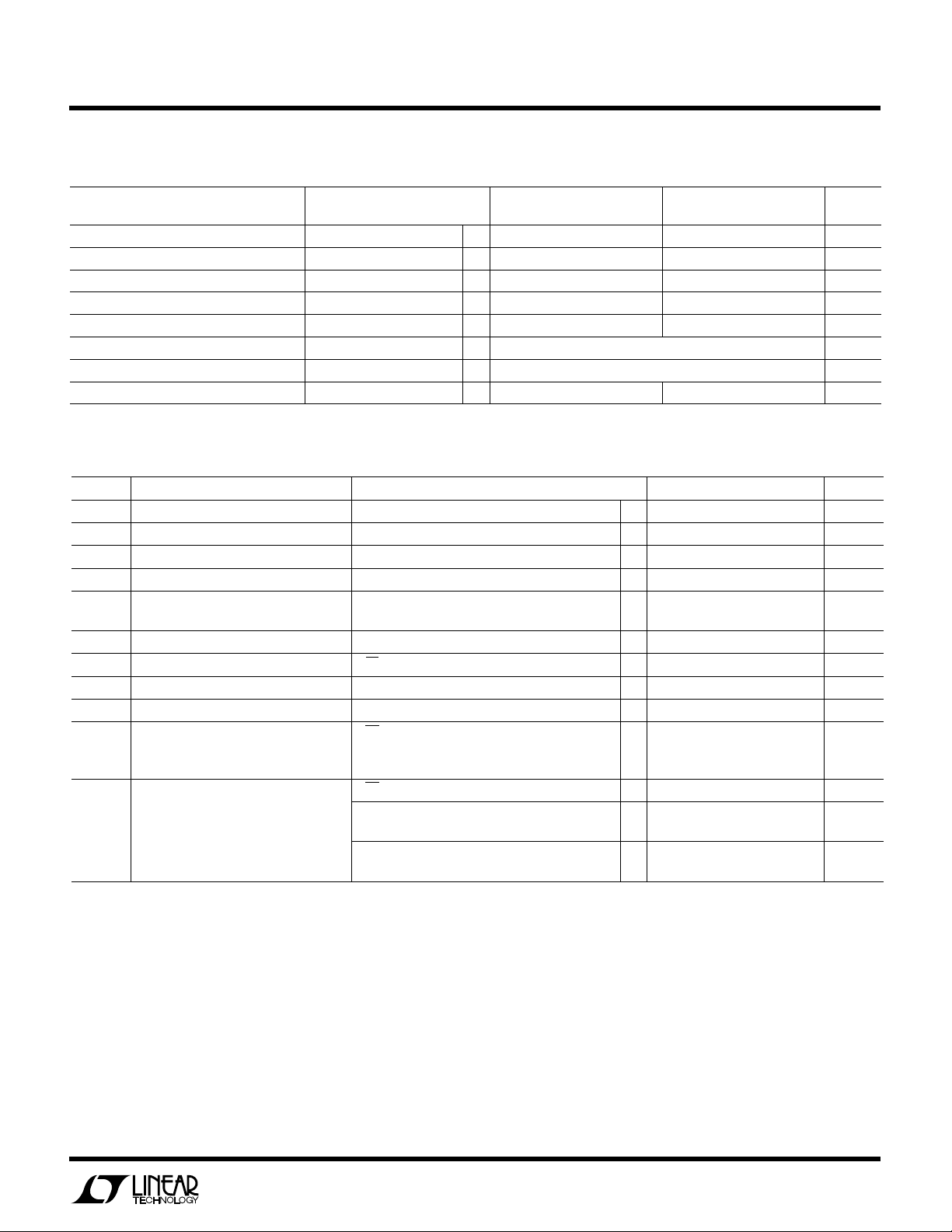
RECO E DED OPERATI G CO DITIO S
SYMBOL PARAMETER CONDITIONS MIN TYP MAX UNITS
V
CC
f
CLK
t
CYC
t
hDI
t
suCS
t
WAKEUP
t
suDI
t
WHCLK
t
WLCLK
t
WHCS
t
WLCS
Supply Voltage 2.65 4.0 V
Clock Frequency VCC = 2.65V 25 250 kHz
Total Cycle Time LTC1096L, f
Hold Time, DIN After CLK↑ VCC = 2.65V 450 ns
Setup Time CS↓ Before First CLK↑ (See Operating Sequence) VCC = 2.65V, LTC1096L 1 µs
Wakeup Time CS↓ Before First CLK↓ After First CLK↑ VCC = 2.65V, LTC1096L 10 µs
(See Figure 1, LTC1096L Operating Sequence)
Wakeup Time CS↓ Before MSBF Bit CLK↓ VCC = 2.65V, LTC1098L 10 µs
(See Figure 2, LTC1098L Operating Sequence)
Setup Time, DIN Stable Before CLK↑ VCC = 2.65V 1 µs
CLK High Time VCC = 2.65V 1.6 µs
CLK Low Time VCC = 2.65V 1.6 µs
CS High Time Between Data Transfer Cycles VCC = 2.65V 2 µs
CS Low Time During Data Transfer LTC1096L, f
LTC1098L, f
VCC = 2.65V, LTC1098L 1 µs
LTC1098L, f
= 250kHz 58 µs
CLK
= 250kHz 58 µs
CLK
= 250kHz 56 µs
CLK
= 250kHz 56 µs
CLK
2
LTC1096L/LTC1098L
UU W
CO VERTER A D ULTIPLEXER CHARACTERISTICS
V
= 2.65V, V
CC
= 2.5V, f
REF
= 250kHz, unless otherwise noted.
CLK
PARAMETER CONDITIONS MIN TYP MAX MIN TYP MAX UNITS
Resolution (No Missing Code) ● 8 8 Bits
Offset Error (Note 4) ● ±0.5 ±1 LSB
Linearity Error ● ±0.5 ±1 LSB
Full Scale Error ● ±0.5 ±1 LSB
Total Unadjusted Error (Note 5) V
Analog Input Range (Note 6) V
REF Input Range (Note 6) 2.65 ≤ VCC ≤ 4.0V V
Analog Input Leakage Current (Note 7) ● ±1 ±1 µA
= 2.5V ● ±1 ±1.5 LSB
REF
LTC1096LA/LTC1098LA
–0.05V to V
–0.05V to V
LTC1096L/LTC1098L
+ 0.05V
CC
+ 0.05V
CC
U
D
DIGITAL
VCC = 2.65V, V
SYMBOL PARAMETER CONDITIONS MIN TYP MAX UNITS
V
IH
V
IL
I
IH
I
IL
V
OH
V
OL
I
OZ
I
SOURCE
I
SINK
I
REF
I
CC
A
= 2.5V, f
REF
High Level Input Voltage VCC = 3.6V ● 1.9 V
Low Level Input Voltage VCC = 2.65V ● 0.45 V
High Level Input Current VIN = V
Low Level Input Current VIN = 0V ● –2.5 µA
High Level Output Voltage VCC = 2.65V, IO = 10µA ● 2.4 2.64 V
Low Level Output Voltage VCC = 2.65V, IO = 400µA ● 0.3 V
Hi-Z Output Leakage CS =High ● ±3 µA
Output Source Current V
Output Sink Current V
Reference Current CS = V
Supply Current CS = V
DC
CLK
LECTRICAL C CHARA TER ST
E
= 250kHz, unless otherwise noted.
CC
I
= 0V –10 mA
OUT
= V
OUT
≥ 200µs, f
t
CYC
= 58µs, f
t
CYC
LTC1096L, t
LTC1098L, t
= 360µA ● 2.1 2.50 V
O
CC
CC
CC
≤ 50kHz ● 3.500 7.5 µA
CLK
= 250kHz ● 35.00 50.0 µA
CLK
≥ 200µs, f
CYC
= 58µs, f
t
CYC
≥ 200µs, f
CYC
= 58µs, f
t
CYC
ICS
I
● 2.5 µA
15 mA
● 0.001 2.5 µA
● 0.001 ± 3 µA
≤ 50kHz ● 40 80 µA
CLK
= 250kHz ● 120 180 µA
CLK
≤ 50kHz ● 44 88 µA
CLK
= 250kHz ● 155 230 µA
CLK
3
 Loading...