

Linear Technology LT1011AMH, LT1011AIS8, LT1011ACN8, LT1011ACJ8, LT1011ACH Datasheet
...
FEATURES
LT1011/LT1011A
Voltage Comparator
U
DESCRIPTIO
■
Pin Compatible with LM111 Series Devices
■
Guaranteed
■
Guaranteed
■
Guaranteed
■
Guaranteed
■
Guaranteed
■
50mA Output Current Source or Sink
■
±30V Differential Input Voltage
■
Fully Specified for Single 5V Operation
Max 0.5mV Input Offset Voltage
Max 25nA Input Bias Current
Max 3nA Input Offset Current
Max 250ns Response Time
Min 200,000 Voltage Gain
U
APPLICATIO S
■
SAR A/D Converters
■
Voltage-to-Frequency Converters
■
Precision RC Oscillator
■
Peak Detector
■
Motor Speed Control
■
Pulse Generator
■
Relay/Lamp Driver
, LTC and LT are registered trademarks of Linear Technology Corporation.
The LT®1011 is a general purpose comparator with significantly better input characteristics than the LM111.
Although pin compatible with the LM111, it offers four
times lower bias current, six times lower offset voltage and
five times higher voltage gain. Offset voltage drift, a
previously unspecified parameter, is guaranteed at
15µV/°C. Additionally, the supply current is lower by a
factor of two with no loss in speed. The LT1011 is several
times faster than the LM111 when subjected to large
overdrive conditions. It is also fully specified for DC
parameters and response time when operating on a single
5V supply. These parametric improvements allow the
LT1011 to be used in high accuracy (≥12-bit) systems
without trimming. In a 12-bit A/D application, for instance,
using a 2mA DAC, the offset error introduced by the
LT1011 is less than 0.5LSB. The LT1011 retains all the
versatile features of the LM111, including single 3V to
±18V supply operation, and a floating transistor output
with 50mA source/sink capability. It can drive loads referenced to ground, negative supply or positive supply, and
is specified up to 50V between V– and the collector output.
A differential input voltage up to the full supply voltage is
allowed, even with ±18V supplies, enabling the inputs to
be clamped to the supplies with simple diode clamps.
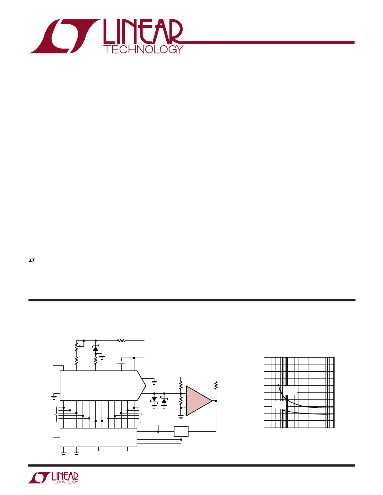
TYPICAL APPLICATIO
10µs 12-Bit A/D Converter
R1
15V
PARALLEL
OUTPUTS
5V
1k
FULL-SCALE
TRIM
R2*
6.49k
20 14 15 16 17
13
10 9 8 7 6 5 4 32
12
11
456789161718192021
24
E
12
LM329
7V
R3
0.001µF
6.98k
6012
12-BIT
D/A CONVERTER
AM2504
SAR REGISTER
SCP
START CLOCK f = 1.4MHz
3.9k
U
1
D
CC
S
15V
–15V
19
18
PARALLEL
OUTPUTS
SERIAL OUTPUT
*R2 AND R4
SHOULD TC TRACK
INPUT
0V TO 10V 5V
R4*
2.49k
2
+
R6
7475
LATCH
3
LT1011A
–
1011 TA01
820Ω
Response Time vs Overdrive
500
450
400
R5
1k
7
350
300
250
200
RISING
150
100
OUTPUT
50
0
0.1
RESPONSE TIME (ns)
FALLING
OUTPUT
1 10 100
OVERDRIVE (mV)
1011 TA02
1
LT1011/LT1011A
WW
W
ABSOLUTE MAXIMUM RATINGS
U
(Note 1)
Supply Voltage (Pin 8 to Pin 4) .............................. 36V
Output to Negative Supply (Pin 7 to Pin 4)
LT1011AC, LT1011C .......................................... 40V
LT1011AI, LT1011I ............................................ 40V
LT1011AM, LT1011M (OBSOLETE) .............. 50V
Ground to Negative Supply (Pin 1 to Pin 4) ............ 30V
Differential Input Voltage ...................................... ±36V
Voltage at STROBE Pin (Pin 6 to Pin 8) .................... 5V
U
W
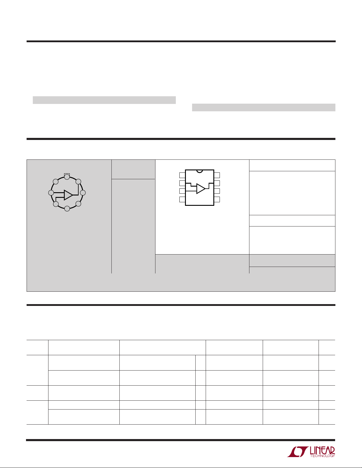
PACKAGE/ORDER INFORMATION
TOP VIEW
+
V
8
1
GND
2
INPUT
INPUT
3
H PACKAGE
8-LEAD TO-5 METAL CAN
T
= 150°C, θJA = 150°C/W, θJC = 45°C/W
JMAX
7
+
–
5
4
–
V
OUTPUT
BALANCE/
6
STROBE
BALANCE
ORDER PART
NUMBER
LT1011ACH
LT1011CH
LT1011AMH
LT1011MH
INPUT
INPUT
Input Voltage (Note 2) ....................... Equal to Supplies
Output Short-Circuit Duration.............................. 10 sec
Operating Temperature Range (Note 3)
LT1011AC, LT1011C ............................... 0°C to 70°C
LT1011AI, LT1011I ........................... –40°C to 85°C
LT1011AM, LT1011M (OBSOLETE) –55°C to 125°C
Storage Temperature Range .................– 65°C to 150°C
Lead Temperature (Soldering, 10 sec).................. 300°C
U
TOP VIEW
GND
1
2
+
–
3
–
V
4
N8 PACKAGE
8-LEAD PDIP
T
= 150°C, θJA = 130°C/ W(N8)
JMAX
= 150°C, θJA = 150°C/ W(S8)
T
JMAX
V+
8
OUTPUT
7
BALANCE/
6
STROBE
BALANCE
5
S8 PACKAGE
8-LEAD PLASTIC SO
ORDER PART NUMBER
LT1011ACN8
LT1011CN8
LT1011CS8
LT1011AIS8
LT1011IS8
S8 PART MARKING
1011
1011AI
1011I
T
JMAX
OBSOLETE PACKAGES
Consider the N8 or S8 Packages for Alternate Source
Consult LTC Marketing for parts specified with wider operating temperature ranges.
J8 PACKAGE 8-LEAD CERDIP
= 150°C, θJA = 100°C/ W(J8)
ORDER PART NUMBER
LT1011ACJ8
LT1011CJ8
LT1011AMJ8
LT1011MJ8
ELECTRICAL CHARACTERISTICS
The ● denotes the specifications which apply over the full operating temperature range, otherwise specifications are at TA = 25°C.
VS = ±15V, VCM = 0V, RS = 0Ω, V1 = –15V, output at pin 7 unless otherwise noted.
LT1011AC/AI/AM LT1011C/I/M
SYMBOL PARAMETER CONDITIONS MIN TYP MAX MIN TYP MAX UNITS
V
OS
I
OS
I
B
Indicates parameters which are guaranteed for all supply voltages, including a single 5V supply. See Note 5.
*
Input Offset Voltage (Note 4) 0.3 0.5 0.6 1.5 mV
● 1.0 3.0 mV
*Input Offset Voltage RS ≤ 50k (Note 5) 0.75 2.0 mV
● 1.50 3.0 mV
*Input Offset Current (Note 5) 0.2 3 0.2 4 nA
● 56nA
Input Bias Current (Note 4) 15 25 20 50 nA
*Input Bias Current (Note 5) 20 35 25 65 nA
● 50 80 nA
2
LT1011/LT1011A
ELECTRICAL CHARACTERISTICS
The ● denotes the specifications which apply over the full operating temperature range, otherwide specifications are at TA = 25°C.
VS = ±15V, VCM = 0V, RS = 0Ω, V1 = –15V, output at pin 7 unless otherwise noted.
LT1011AC/AI/AM LT1011C/I/M
SYMBOL PARAMETER CONDITIONS MIN TYP MAX MIN TYP MAX UNITS
∆V
OS
∆T (Note 6)
A
VOL
CMRR Common Mode 94 115 90 115 dB
t
D
V
OL
Input Offset Voltage Drift T
*Large-Signal Voltage Gain RL = 1k to 15V, 200 500 200 500 V/mV
Rejection Ratio
*Input Voltage Range VS = ±15V ● –14.5 13 –14.5 13 V
(Note 9) V
*Response Time (Note 7) 150 250 150 250 ns
*Output Saturation Voltage, VIN = 5mV, I
V
= 0 VIN = 5mV, I
1
*Output Leakage Current VIN = 5mV, V1 = –15V, 0.2 10 0.2 10 nA
*Positive Supply Current 3.2 4.0 3.2 4.0 mA
*Negative Supply Current 1.7 2.5 1.7 2.5 mA
*Strobe Current Minimum to Ensure Output 500 500 µA
(Note 8) Transistor is Off
Input Capacitance 6 6 pF
≤ T ≤ T
MIN
–10V ≤ V
RL = 500Ω to 5V, 50 300 50 300 V/mV
0.5V ≤ V
= Single 5V ● 0.5 3 0.5 3 V
S
= 5mV, I
V
IN
V
OUT
MAX
≤ 14.5V
OUT
≤ 4.5V
OUT
= 8mA, TJ ≤ 100°C 0.25 0.40 0.25 0.40 V
SINK
= 8mA ● 0.25 0.45 0.25 0.45 V
SINK
= 50mA ● 0.70 1.50 0.70 1.50 V
SINK
= 35V (25V for LT1011C/I) ● 500 500 nA
● 415 425µV/°C
Indicates parameters which are guaranteed for all supply voltages, including a single 5V supply. See Note 5.
*
Note 1: Absolute Maximum Ratings are those values beyond which the
life of a device may be impaired.
Note 2: Inputs may be clamped to supplies with diodes so that
maximum input voltage actually exceeds supply voltage by one diode
drop. See Input Protection in the Applications Information section.
Note 3: T
Note 4: Output is sinking 1.5mA with V
Note 5: These specifications apply for all supply voltages from a single
5V to ±15V, the entire input voltage range, and for both high and low
output states. The high state is I
the low state is I
defines a worst-case error band that includes effects due to common
mode signals, voltage gain and output load.
JMAX
= 150°C.
≤ 8mA, V
SINK
= 0V.
OUT
≥ 100µA, V
SINK
≤ 0.8V. Therefore, this specification
OUT
≥ (V+ – 1V) and
OUT
Note 6: Drift is calculated by dividing the offset voltage difference
measured at min and max temperatures by the temperature difference.
Note 7: Response time is measured with a 100mV step and 5mV
overdrive. The output load is a 500Ω resistor tied to 5V. Time
measurement is taken when the output crosses 1.4V.
Note 8: Do not short the STROBE pin to ground. It should be current
driven at 3mA to 5mA for the shortest strobe time. Currents as low as
500µA will strobe the LT1011A if speed is not important. External
leakage on the STROBE pin in excess of 0.2µA when the strobe is “off”
can cause offset voltage shifts.
Note 9: See graph “Input Offset Voltage vs Common Mode Voltage.”
3
LT1011/LT1011A
UW
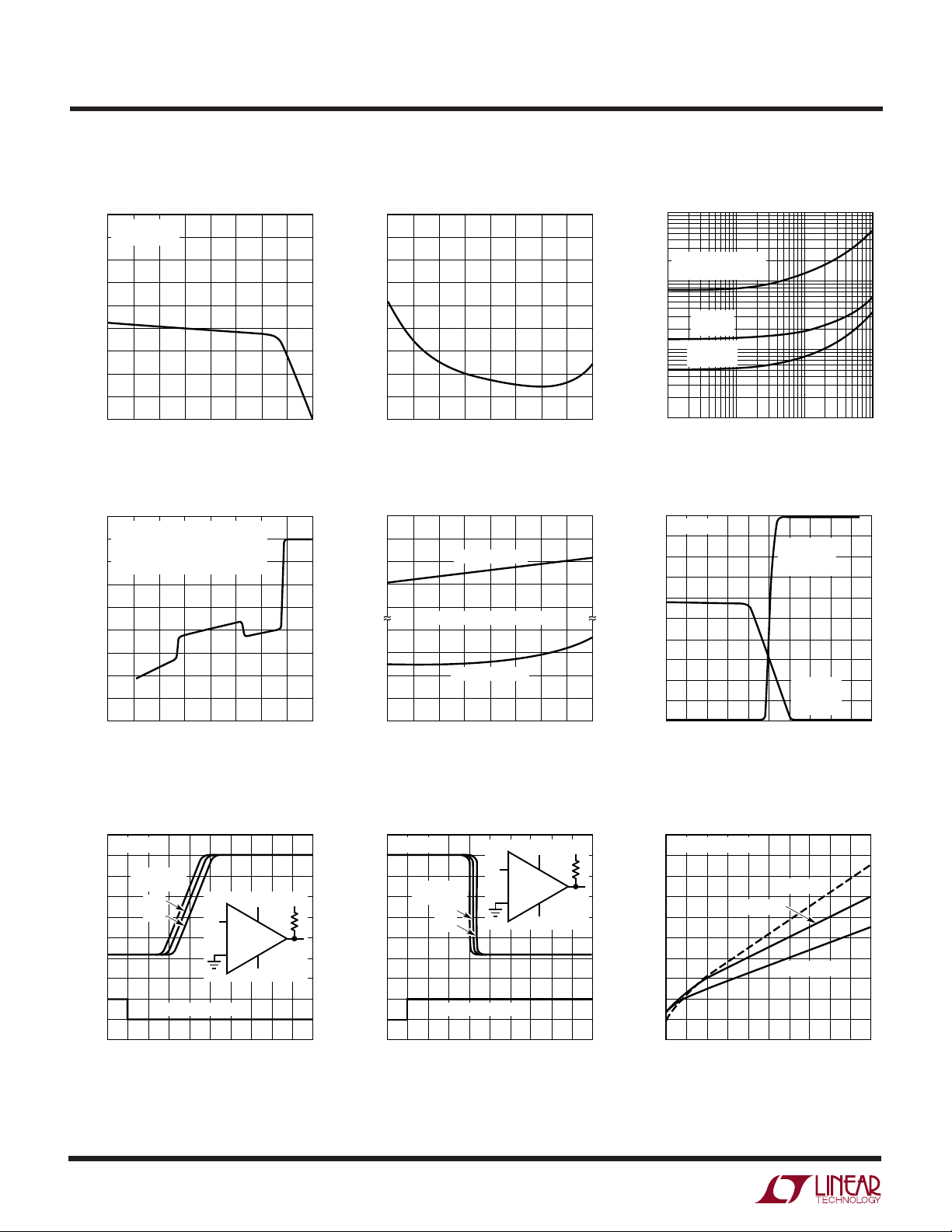
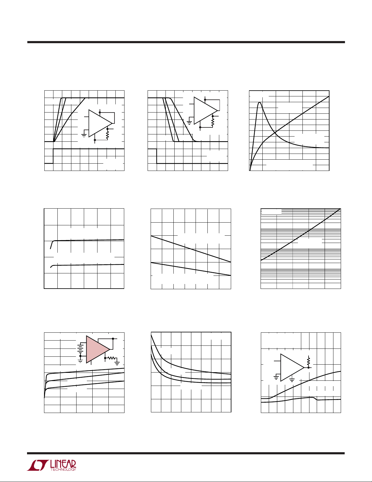
TYPICAL PERFOR A CE CHARACTERISTICS
Input Bias Current Input Offset Current Worst-Case Offset Error
45
IB FLOWS OUT
40
OF INPUTS
35
30
25
20
CURRENT (nA)
15
10
5
0
–50
–25
0
50 75 100 125
25
TEMPERATURE (°C)
150
1011 G01
0.9
0.8
0.7
0.6
0.5
0.4
CURRENT (nA)
0.3
0.2
0.1
0
–50
–25
0
50 75 100 125
25
TEMPERATURE (°C)
150
1011 G01
Input Characteristics* Common Mode Limits Transfer Function (Gain)
+
5
*EITHER INPUT.
0
REMAINING INPUT GROUNDED.
CURRENT FLOWS OUT OF INPUT.
–5
= ±15V
V
S
–10
–15
–20
–25
INPUT CURRENT (nA)
–30
–35
–40
–20
–15
–10
–5
INPUT VOLTAGE (V)
0 5 10 15
20
1011 G04
V
–0.5
–1.0
–1.5
–2.0
0.4
0.3
0.2
COMMON MODE VOLTAGE (V)
0.1
–
V
–50
–25
POSITIVE LIMIT
REFERRED TO SUPPLIES
NEGATIVE LIMIT
0
25
TEMPERATURE (°C)
50 75 100 125
150
1011 G05
100
LM311
(FOR COMPARISON)
10
LT1011M
LT1011C
LT1011AM
1
LT1011AC
EQUIVALENT OFFSET VOLTAGE (mV)
0.1
1k
50
TA = 25°C
40
30
20
OUTPUT VOLTAGE (V)
10
0
– 0.5
10k 100k 1M
SOURCE RESISTANCE (Ω)
–0.3
DIFFERENTIAL INPUT VOLTAGE (mV)
–0.1
COLLECTOR
OUTPUT
= 1k
R
L
EMITTER
OUTPUT
R
= 600Ω
L
0.1
0.3
1011 G03
0.5
1011 G06
Response Time—Collector Output Response Time—Collector Output
100mV
6
VS = ±15V
5
4
3
2
1
0
0
OVERDRIVE
20mV
5mV
2mV
INPUT = 100mV STEP
50 100
0
150
V
IN
200
TIME (ns)
15V 5V
500Ω
–
+
–15V
250 300 400
350
450
1011 G07
100mV
6
5
4
3
2
1
0
0
VS = ±15V
OVERDRIVE
INPUT = 100mV STEP
50 100
0
20mV
5mV
2mV
150
200
TIME (ns)
V
–
IN
+
250 300 400
4
15V 5V
500Ω
–15V
350
1011 G08
450
Collector Output Saturation
Voltage
1.0
PIN 1 GROUNDED
0.9
0.8
0.7
0.6
0.5
0.4
0.3
SATURATION VOLTAGE (V)
0.2
0.1
0
50
TA = 25°C
10 15
20
SINK CURRENT (mA)
25
TA = 125°C
TA = –55°C
30 35 45
40
50
1011 G09
UW
TYPICAL PERFOR A CE CHARACTERISTICS
LT1011/LT1011A
Response Time Using GND Pin
as Output
15
20mV 5mV 2mV
10
5
0
–5
–10
OUTPUT VOLTAGE (V)
–15
0
–50
–100
INPUT VOLTAGE (mV)
0
1
V
IN
TIME (µs)
+
V
V
OUT
2k
–
V
= ±15V
V
S
= 25°C
T
A
4
3
2
1011 G10
Response Time Using GND Pin
as Output
15
V
10
5
0
–5
–10
–15
20mV
0
–50
–100
INPUT VOLTAGE (mV) OUTPUT VOLTAGE (V)
0
IN
5mV
1
TIME (µs)
2
Supply Current vs Supply Voltage Supply Current vs Temperature
5
4
3
2
CURRENT (mA)
1
0
0
POSITIVE SUPPLY
COLLECTOR OUTPUT “LO”
POSITIVE AND NEGATIVE SUPPLY
COLLECTOR OUTPUT “HI”
10 15 20
5
SUPPLY VOLTAGE (V)
25 30
1011 G13
6
5
4
3
CURRENT (mA)
2
1
POSITIVE AND NEGATIVE SUPPLY
COLLECTOR OUTPUT “HI”
0
–50
–25 0
TEMPERATURE (˚C)
POSITIVE SUPPLY
COLLECTOR OUTPUT “LO”
50 100 125
25 75
2mV
Output Limiting Characteristics*
+
V
V
OUT
2k
–
V
140
120
100
80
60
TA = 25°C
POWER
DISSIPATION
SHORT-CIRCUIT
CURRENT
40
= ±15V
V
S
T
A
3
= 25°C
SHORT-CIRCUIT CURRENT (mA)
20
0
4
0
*MEASURED 3 MINUTES
AFTER SHORT
5
10 15
OUTPUT VOLTAGE (V)
1011 G11
1011 G12
0.7
0.6
POWER DISSIPATION (W)
0.5
0.4
0.3
0.2
0.1
0
Output Leakage Current
–7
10
VS = ±15V
–8
10
V
= 35V
OUT
= –15V
V
GND
TEMPERATURE (
°C)
1011 G15
1011 G14
–9
10
–10
LEAKAGE CURRENT (A)
10
–11
10
25 65 85 105
45 125
Output Saturation—
Ground Output
5
REFERRED TO V
4
3
TJ = –55°C
2
TO GROUND PIN VOLTAGE (V)
1
+
V
0
0
+
TJ = 25°C
TJ = 125°C
10
20
OUTPUT CURRENT (mA)
Output Saturation Voltage Response Time vs Input Step Size
+
2
+
8
LT1011
3
4
–
V
V
7
1
R
L
V
OUT
0.6
0.5
0.4
0.3
0.2
= 125°C
T
J
= 25°C
T
J
TJ = –55°C
I
SINK
= 8mA
SATURATION VOLTAGE (V)
0.1
0
30
40
50
0
24
13
6
5
8
7
INPUT OVERDRIVE (mV)
1011 G16
1011 G17
1000
VS = ±15V
= 500Ω TO 5V
R
L
OVERDRIVE = 5mV
800
–
3
INPUT
600
2
+
400
PROPAGATION DELAY (ns)
200
0
2
3
19
0
INPUT STEP (V)
1
4
5V
500Ω
7
RISING INPUT
FALLING INPUT
6
5
7
8
10
1011 G18
5
 Loading...