


VS750
1. Introduction
1.1. Purpose
This manual provides the information necessary to repair, calibration, description and download the
features of this model.
1.2. Regulatory Information
A. Security
Toll fraud, the unauthorized use of telecommunications system by an unauthorized part (for example,
persons other than your company’s employees, agents, subcontractors, or person working on your
company’s behalf) can result in substantial additional charges for your telecommunications services.
System users are responsible for the security of own system.
There are may be risks of toll fraud associated with your telecommunications system. System users
are responsible for programming and configuring the equipment to prevent unauthorized use. The
manufacturer does not warrant that this product is immune from the above case but will prevent
unauthorized use of common carrier telecommunication service of facilities accessed through or
connected to it. The manufacturer will not be responsible for any charges that result from such
unauthorized use.
B. Incidence of Harm
If a telephone company determines that the equipment provided to customer is faulty and possibly
causing harm or interruption in service to the telephone network, it should disconnect telephone
service until repair can be done. A telephone company may temporarily disconnect service as long as
repair is not done.
C. Changes in Service
A local telephone company may make changes in its communications facilities or procedure. If these
changes could reasonably be expected to affect the use of the phones or compatibility with the net
work, the telephone company is required to give advanced written notice to the user, allowing the user
to take appropriate steps to maintain telephone service.
D. Maintenance Limitations
Maintenance limitations on the phones must be performed only by the manufacturer or its authorized
agent. The user may not make any changes and/or repairs expect as specifically noted in this manual.
Therefore, note that unauthorized alternations or repair may affect the regulatory status of the system
and may void any remaining warranty.
E. Notice of Radiated Emissions
This model complies with rules regarding radiation and radio frequency emission as defined by local
regulatory agencies. In accordance with these agencies, you may be required to provide information
such as the following to the end user.
F. Pictures
The pictures in this manual are for illustrative purposes only; your actual hardware may look slightly
different.
G. Interference and Attenuation
A phone may interfere with sensitive laboratory equipment, medical equipment, etc. Interference from

VS750
unsuppressed engines or electric motors may cause problems.
H. Electrostatic Sensitive Devices
ATTENTION
Boards, which contain Electrostatic Sensitive Device (ESD), are indicated by the sign. Following
information is ESD handling:
• Service personnel should ground themselves by using a wrist strap when exchange system boards.
• When repairs are made to a system board, they should spread the floor with anti-static mat which is
also grounded.
• Use a suitable, grounded soldering iron.
• Keep sensitive parts in these protective packages until these are used.
• When returning system boards or parts like EEPROM to the factory, use the protective package as
described.

VS750 Product SPEC
- 1 -
VS750
Product Requirement SPEC.
Feb., 26, 2010
(RevA.0)
LG Electronics Inc.

VS750
- 2 -
Table of Contents
VS750 Product SPEC........................ 1
2. Supporting Standard................................. 3
3. Functions of Major Semi-Conductors ....... 3
4. HW Features ............................................ 4
5. SW Features............................................. 6
6. VS750 Figures.......................................... 9
GSM/ UMTS TECHNICAL BRIEF.... 10
1.1. GENERAL DESCRIPTION.................. 10
1.2. GSM MODE......................................... 11
1.3. UMTS MODE....................................... 13
1.4. LO GENERATION and DISTRIBUTION
CIRCUIT .............................................. 16
1.5. OFF-CHIP RF COMPONENTS ........... 17
Calibration & RF Auto Test
Program (Tachyon)......................... 85
1. Configuration of Tachyon ....................... 86
1.1 Configuration of directory............... 86
1.2 Description of basic folders............ 87
1.3 Description of configuration files.... 87
2. How to use Tachyon............................... 88
2.1 Model selection.............................. 88
2.2 Start cal & auto .............................. 90
Main PCB Component List............. 92
FPCB Main Component List ........113
3 Key Component List.................. 114
TROUBLE SHOOTING .................... 21
1.1 RF Component ..................................... 21
1.2 SIGNAL PATH...................................... 23
1.3 Checking TCXO Block.......................... 26
1.4 Checking FEM Block ............................ 28
1.5 Checking WCDMA Block...................... 31
1.6 Checking GSM Block............................ 43
System HW Block Diagram............ 52
System RF Block Diagram............. 53
System HW Block Diagram............ 54
VS750 REV 1.0 Schematic.............. 57
BGA Pin Map ...................................77
VS750 Product SPEC
- 3 -
VS750 : WCDMA1900/850/2100 + EGSM/GSM850/DCS/PCS +
US Cellular/US PCS + GPS
(HSDPA / GPRS / EDGE) (EVDO Rev_0 / EVDO Rev_A)
2. Supporting Standard
tnemmoC erutaeF metI
Supporting
Standard
Frequency Range WCDMA(FDD1) TX : 1920 – 1980 MHz
WCDMA(FDD1,2,5)
EGSM/GSM850/DCS1800/PCS1900
US Cellular / US PCS
GPS
WCDMA(FDD1) RX : 2110 – 2170 MHz
WCDMA(FDD2) TX : 1850 – 1910 MHz
WCDMA(FDD2) RX : 1930 – 1990 MHz
WCDMA(FDD5) TX : 824 – 849 MHz
WCDMA(FDD5) RX : 849 – 894 MHz
EGSM TX : 880 – 915 MHz
EGSM RX : 925 – 960 MHz
GSM850 TX : 824 – 849 MHz
GSM850 RX : 869 – 894 MHz
DCS1800 TX : 1710 – 1785 MHz
DCS1800 RX : 1805 – 1880 MHz
PCS1900 TX : 1850 – 1910 MHz
PCS1900 RX : 1930 – 1990 MHz
US Cellular TX : 824.82 ~ 848.19 MHz
US Cellular RX : 869.82~893.19 MHz
US PCS TX : 1850~1910 MHz
US PCS RX : 1930~1990 MHz
GPS : 1575.42 MHz
3. Functions of Major Semi-Conductors
noitcnuF noitacifissalC
QSD8650 Terminal operation control and digital signal processing
Memory
(H8BES0UQ0MCR-46M)
RTR6500/ RTR6285 Converts Rx and Tx RF signal to baseband signal
NAND Flash Memory (4G) + SDRAM (2G)
Storing of terminal operation program
VS750 Product SPEC
- 4 -
4. HW Features
Form Factor Horizontal Slide QWERTY
Battery
Size Standard :
PCB 3-8 Staggered 10 Layers , 0.8t
Stand by time GSM Up to 370 hrs
Talk time GSM Up to 250 min
SIM card type Plug-In SIM
LCD
Built-in Camera 3.0 Mega AF Camera w/o Flash
Keypad Function Key : 4
ANT Main : Internal Fixed Type
Ear Phone Jack
Memory NAND Flash : 4Gbit
Data & Fax Built in Data & Fax support
Blue Tooth V2.1 + EDR
MIDI(for Buzzer
Function)
1) Capacity
Standard : Li-Ion polymer, 1500mAh
2) Packing Type : Soft Pack
115 x 56 x 16.5 mm
WCDMA Up to 300 hrs
CDMA Up to 240 hrs
WCDMA Up to 300 min
CDMA Up to 150 min
3V /1.8V
3.2” 800 x 480 pixels (WVGA)
260K TFT LCD
Side Key : 2
3.5Φ Ear Jack
SDRAM : 2Gbit
SW Decoded 72Poly
g 051 thgieW
DBT emuloV
@ Paging Period 5 (2G)
@ DRX 7 (3G)
@ SCI=2(pwr: -75dBm)
1500mAh
@ TX= Lvl 5 (2G)
@ Tx = 12dBm (3G)
@ Rx pwr -92dBm
rotacidnI BGR rotacidnI sutatS
Function Key:
CAM, Power, HW Reset,
Mullti Tasking
Side Key :
Volume up/down
niP 5 rotcennoc metsyS
RMA,RH ,RFE ,RF gnidoc hceepS
rotarbiV ni tliuB rotarbiV
+CAA/CAA/3PM reyalP cisuM
,462.H ,4GEPM reyalP oediV
tnemmoC erutaeF metI
/ ffO rewoP @ nim 003 emit gnigrahC
462.H ,4GEPM redrocmaC
seY gnidroceR ecioV
seYedom enohP rekaepS

VS750 Product SPEC
- 5 -
Support
T-Flash
(External Memory)
seY retpadA levarT
seY MORDC
seY tesdaeH oeretS
seY elbaC ataD
seY
VS750 Product SPEC
- 6 -
5. SW Features
RSSI 0 ~ 5 Levels
Battery Charging 0 ~ 4 Levels
Key Volume 0 ~ 5 Level
Audio Volume 0 ~ 5 Level
Quick Access Mode Dialing/ Contact / Camera
Phone Book [Outlook contact]
Name / Picture / Company /
File as: / Mobile tel / Work tel /
Home tel / Work2 tel / Home2
tel / Company tel / Pager / Car
tel / Assistant tel / Radio tel /
E-mail / IM / E-mail2 / E-mail3
/ IM2 / IM3 / Set ringtone /
Work addr: / Home addr: /
Other addr: / Job title: / Office
loc: / Work fax / Home fax /
Birthday / Anniversary /
Categories / Web page /
Spouse / Children /
Department / Assistant /
Manager / Customer ID / Govt
ID / Account / Note
[SIM Contact]
Name / Tel number
Last Received
Number
Search by Number
/ Name
tnemmoC erutaeF metI
seY yalpsiD etaD / emiT
hsilgnE oN egaugnaL-itluM
SM(cnys evitcA htiw troppuS seY cnyS CP
application). Contacts, Calendar,
E-mail, Tasks, Notes, Favorites,
Files, Media
yek 1 >- retnec liam ecioV seY laiD deepS
enohp erutaef htiw emas ton seY eliforP
setting
seY RILC / PILC
There is no limitation on the
number of items.
It depends on Available memory
amount.
tsaL ,srebmuN laiD tsaL seY rebmuN laiD tsaL
Received Numbers and Last
Missed Numbers can store.
tsaL ,srebmuN laiD tsaL seY
Received Numbers and Last
Missed Numbers can store .
tsaL ,srebmuN laiD tsaL seY rebmuN dessiM tsaL
Received Numbers and Last
Missed Numbers can store.
emaN
eht no noitatimil on si erehT seY puorG
number of items.

VS750 Product SPEC
- 7 -
Network Selection Automatic /Manual
SMS (EMS) There is no limitation on the
number of items.
It depends on available
memory amount.
EMS Melody / Picture
Send / Receive / Save NoNo
MMS MPEG4
Send / Receive / Save
Download Over the Web
Download Melody /
Wallpaper
Yes
Yes
It depends on
available memory amount.
seY rebmuN laiD dexiF
oN rebmuN laiD ecivreS
ylno daeR seY rebmuN nwO
(add/edit/delete are not
supported)
redrocer eciov troppuS seY omeM ecioV
oN rednimeR llaC
seY etuM
seY treviD llaC
seY gnirraB llaC
oN )CoA( egrahC llaC
seY noitaruD llaC
EMS does not support.
seY SRPG revO SMS
seY egasseM gnoL
oN tsacdaorB lleC
seY emaG
seY radnelaC
eht no noitatimil on si erehT seY omeM
number of items.
It depends on available memory
amount.
seY kcolC dlroW
oN trevnoC tinU
oN hctaW potS
seY repaP llaW
eliboM EI seY resworB PAW
resworb bew revO seY
tnednepeD rotarepO seY kcoL MIS
oN tiklooT MIS
tneilC SMM GL seY SMM
oN SNOE
oN SHPC
/ FA M2.3 seY aremaC
Digital Zoom : x3.2
oN AVAJ
dnammoc eciov htiw troppuS seY laiD ecioV

VS750 Product SPEC
- 8 -
oN aDrI
RDE+1.2 .reV seY htooteulB
(HSP,HFP,A2DP,AVRCP)
oN oidar MF
21 ssalC seY SRPG
21 ssalC seY EGDE
seY eveirteR / dloH
3 .xaM seY llaC ecnerefnoC
seY FMTD
oN dap omeM
seY YTT
seY RMA
seY LMcnyS
seY MI
seY liamE
VS750 Product SPEC
- 9 -
6. VS750 Figures
LG-VS750
- 10 -
3.13 GSM/ UMTS TECHNICAL BRIEF
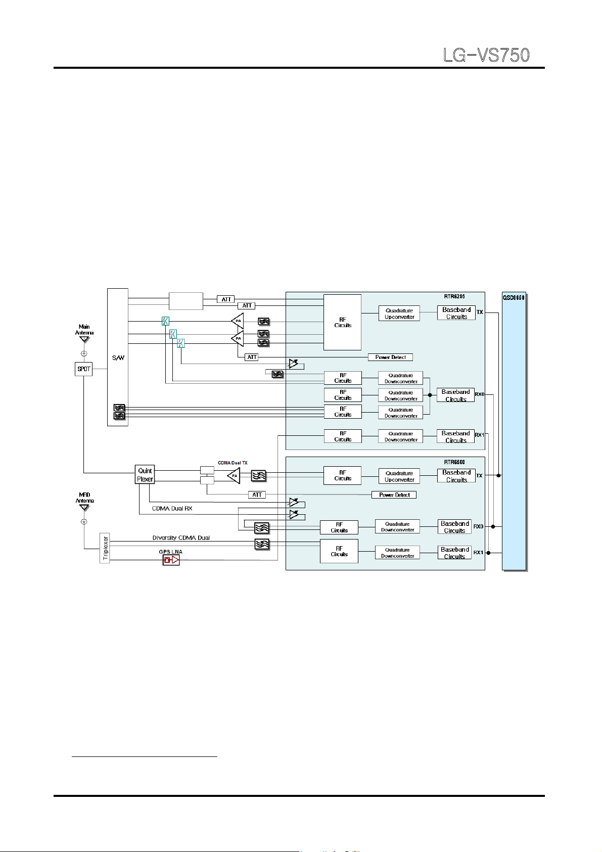
1.1. GENERAL DESCRIPTION
The LG-VS750 supports UMTS-900(Band VIII), UMTS-1900(Band II), UMTS-2100(Band I),
GSM-850, GSM-900, GSM-1800, and GSM-1900 based GSM/GPRS/EDGE/UMTS. All
receivers and the UMTS transmitter use the radioOne1Zero-IF architecture to eliminate
intermediate frequencies, directly converting signals between RF and baseband. The quadband GSM transmitters use a baseband-to-IF up-conversion followed by an offset phaselocked loop that translates the GMSK-modulated or 8-PSK-modulated signal to RF.
GSM_BAND
Quadband
Dual PA
WCDMA_TX_1900
WCDMA_TX_900
WCDMA_TX_2100
GSM Quad
coupler
coupler
[Figure 1-1] Block diagram of RF part
A generic, high-level functional block diagram of LG-VS750 is shown in Figure 1-1. One
antenna collects base station forward link signals and radiates handset reverse link signals.
The antenna connects with receive and transmit paths through LMSP43QL-771(FEM, Front
End Module). The UMTS receive paths each include an LNA, an RF band-pass filter, and a
down-converter that translate the signal directly from RF-to-baseband using radioOne ZIF
techniques. The RFIC’s RX analog baseband outputs, for the receive chains, connect to the
QSD IC. The UMTS and GSM RX baseband outputs share the same inputs to the QSD IC.
For the transmit chains, the RTR6285 IC directly translates the TX baseband signals (from the
QSD 8650 device) to
1
QUALCOMM’s branded chipset that implements a Zero-IF radio architecture.
an RF signal using an internal LO generated by integrated on-chip PLL
LG-VS750
- 11 -
and VCO. The RTR6285 IC outputs deliver fairly high-level RF signals that are first filtered
by TX SAWs and then amplified by their respective UMTS PAs.
In the GSM receive path, the received RF signals are applied through their band-pass filters
and down-converted directly to baseband in the RTR6285 transceiver IC. These baseband
outputs are shared with the UMTS receiver and routed to the QSD IC for further signal
processing.
The GSM/EDGE transmit path employs one stage of up-conversion and, in order to improve
efficiency, is divided into phase and amplitude components to produce an open-loop Polar
topology:
1. The on-chip quadrature up-converter translates the GMSK-modulated signal or 8-PSK
modulated signal, to a constant envelope phase signal at RF;
2. The amplitude-modulated (AM) component is applied to the ramping control pin of Polar
power amplifier from a DAC within the QSD
LG-VS750 power supply voltages are managed and regulated by the PM7540 Power
Management IC. This versatile device integrates all wireless handset power management,
general housekeeping, and user interface support functions into a single mixed signal IC. It
monitors and controls the external power source and coordinates battery recharging while
maintaining the handset supply voltages using low dropout, programmable regulators.
The device’s general housekeeping functions include an ADC and analog multiplexer circuit
for monitoring on-chip voltage sources, charging status, and current flow, as well as userdefined off-chip variables such as temperature, RF output power, and battery ID. Various
oscillator, clock, and counter circuits support IC and higher-level handset functions. Key
parameters such as under-voltage lockout and crystal oscillator signal presence are monitored
to protect against detrimental conditions.
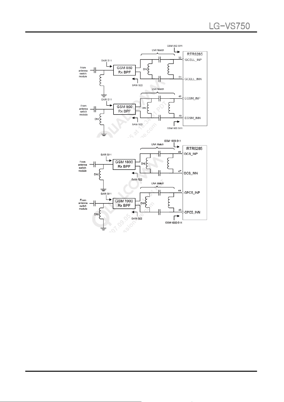
1.2. GSM MODE
1.2.1 GSM RECEIVER
The GSM-850, GSM-900, GSM-1800, and GSM-1900 receiver inputs of RTR6285 are
connected directly to the transceiver front-end circuits(filters and antenna switch module).
GSM-850, GSM-900, GSM-1800, and GSM-1900 receiver inputs use differential
configurations to improve common-mode rejection and second-order non-linearity
performance as shown in Figure 1-2. The balance between the complementary signals is
critical and must be maintained from the RF filter outputs all the way into the IC pins
LG-VS750
- 12 -
[Figure 1-2] GSM Receiver Inputs Topologies
Since GSM-850, GSM-900, GSM-1800, and GSM-1900 signals are time-division duplex (the
handset can only receive or transmit at one time), switches are used to separate RX and TX
signals in place of frequency duplexers – this is accomplished in the switch module. The
GSM-850, GSM-900, GSM-1800, and GSM-1900 receive signals are routed to the RTR6285
through band selection filters and matching networks that transform single-ended 50Ω�sources to differential impedances optimized for gain and noise figure. The RTR input uses
a differential configuration to improve second-order inter-modulation and common mode
rejection performance. The RTR6285 input stages include QSD-controlled gain adjustments
that maximize receiver dynamic range.
The amplifier outputs drive the RF ports of the quadrature RF-to-baseband downconverters.
The downconverted baseband outputs are multiplexed and routed to lowpass filters (one I and
one Q) having passband and stopband characteristics suitable for GMSK or 8-PSK processing.
These filter circuits include DC offset
on to the QSD8650 IC for further processing as shown in Figure 1-7.
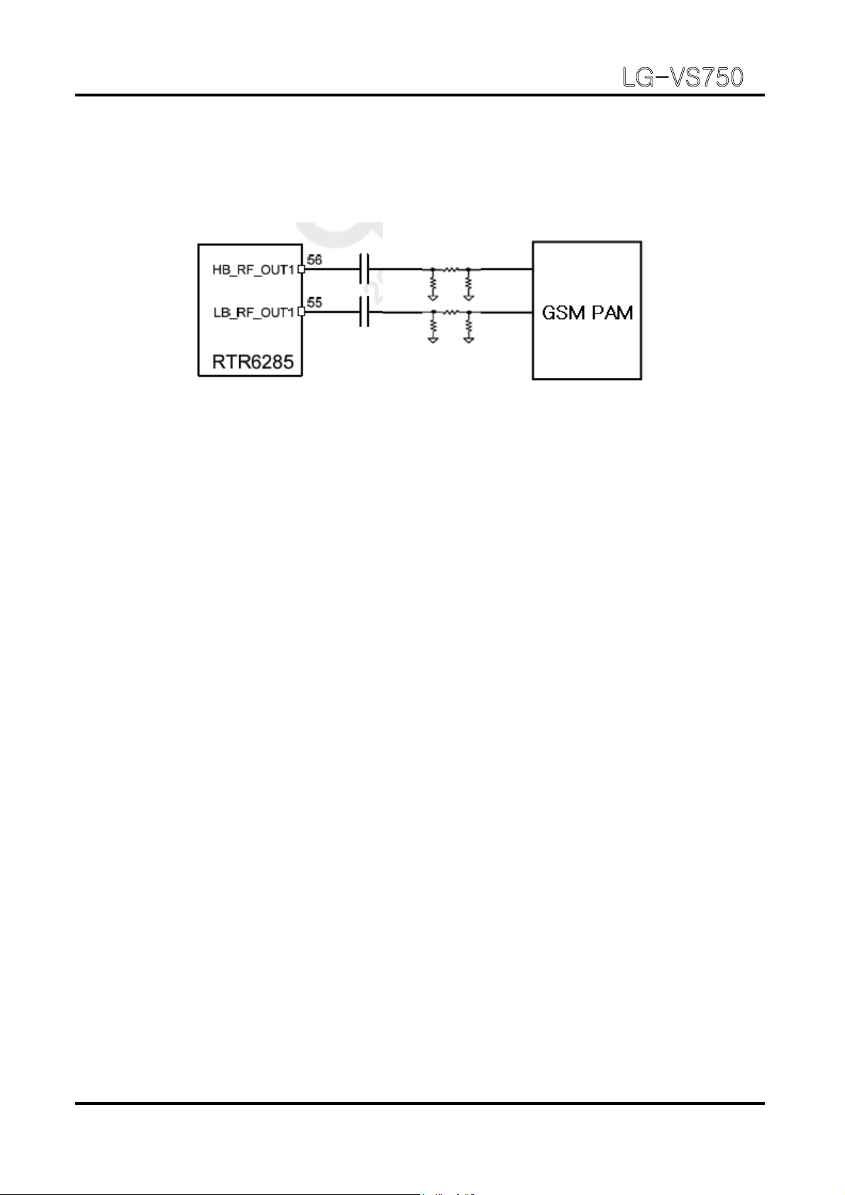
1.2.2 GSM TRANSMITTER
The RTR6285 transmitter outputs(HB_RF_OUT1 and LB_RF_OUT1) include on-chip output
corrections. The filter outputs are buffered and passed
LG-VS750
- 13 -
matching inductors. 50ohm output impedance is achieved by adding a series capacitor at the
output pins. The capacitor value may be optimized for specific applications and PCB
characteristics based on pass-band symmetry about the band center frequency as shown in
Figure 1-3.
[Figure 1-3] GSM Transmitter Outputs Topologies
The RTR6285 IC is able to support GSM 900 and GSM 1800/1900 mode transmitting. This
design guideline shows a tri-band GSM application. Both high-band and low band outputs are
followed by resistive pads to ensure that the load presented to the outputs remains close to
50ohm.
1.3. UMTS MODE
1.3.1 UMTS RECEIVER
The UMTS duplexer receiver output is routed to LNA circuits within the RTR6285 device as
shown in Figure 1-4. The UMTS RX input is provided with an on-chip LNA that amplifies the
signal before a second stage filter that provides differential downconverter as shown in Figure
1-5. This second stage input is configured differentially to optimize second-order
intermodulation and common mode rejection performance. The gain of the UMTS front end
amplifier and the UMTS second stage differential amplifier are adjustable, under QSD control,
to extend the dynamic range of the receivers. The second stage UMTS RX amplifiers drive
the RF ports of the quadrature RF-to-baseband downconverters. The downconverted UMTS
RX
baseband outputs are routed to lowpass filters having passband and stopband
characteristics suitable for UMTS RX processing. These filter circuits allow DC offset
corrections, and their differential outputs are buffered to interface shared with GSM RX to the
QSD IC. The UMTS baseband outputs are turned off when the RTR6285 is downconverting
GSM signals and on when the UMTS is operating.
LG-VS750
- 14 -
[Figure 1-4] UMTS Receiver Inputs Topologies
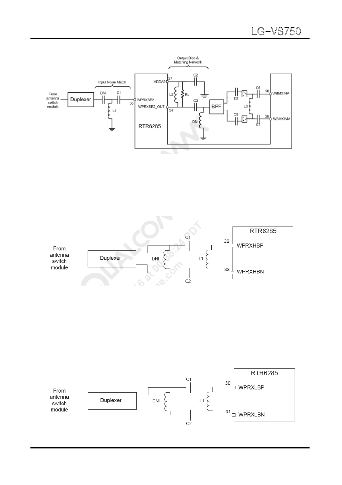
The UMTS-1900 (Band II) receiver LNA input uses a differential configuration with
connections realized by these two pins. The positive and negative connections are WPRXHBP
(pin 32) and WPRXHBN (pin 33), respectively. The WCDMA Rx input is routed from the
duplexer through an impedance transformation circuit that transforms the 50 Ω impedance to
one that is optimally matched to the balance LNA input pins. This is shown in Figure 1-5.
[Figure 1-5] UMTS-1900 (Band II) Receiver Inputs Topologies
The UMTS-900 (Band VIII) receiver LNA input uses a differential configuration with
connections realized by these two pins. The positive and negative connections are WPRXLBP
(pin 30) and WPRXLBN (pin 31), respectively. The WCDMA Rx input is routed from the
duplexer through an impedance transformation circuit that transforms the 50 Ω impedance to
one that is optimally matched to the balance LNA input pins. This is shown in Figure 1-6.
[Figure 1-6] UMTS-900 (Band VIII) Receiver Inputs Topologies

LG-VS750
- 15 -
1.3.2 UMTS TRANSMITTER
The UMTS TX path begins with differential baseband signals (I and Q) from the QSD device.
These analog input signals are amplified, filtered, and applied to the quadrature up-converter
mixers. The up-converter output is amplified by multiple variable gain stages that provide
transmit AGC control. The AGC output is filtered and applied to the driver amplifier; this
output stage includes an integrated matching inductor that simplifies the external matching
network to a single series capacitor to achieve the desired 50-Ω interface.
The RTR6285 UMTS output is routed to its power amplifier through a bandpass filter, and
delivers fairly high-level signals that are filtered and applied to the PA. Transmit power is
delivered from the duplexer to the antenna through the switch module.
The transceiver LO synthesizer is contained within the RTR6285 IC with the exception of the
off-chip loop filter components and the VC-TCXO. This provides a simplified design for
multimode applications. The PLL circuits include a reference divider, phase detect
pump, feedback divider, and digital logic generator.
UMTS TX Using only PLL1, the LO generation and distribution circuits create the necessary
LO signals for nine different frequency converters. The UMTS transmitter also employs the
ZIF architecture to translate the signal directly from baseband to RF. This requires FLO to
equal FRF, and the RTR6285 IC design achieves this without allowing FVCO to equal FRF.
The RTR6285 IC is able to support UMTS 2100/1900/1800/1700 and 900 mode transmitting.
This design guideline shows only UMTS 2100 applications.
or, charge
LG-VS750
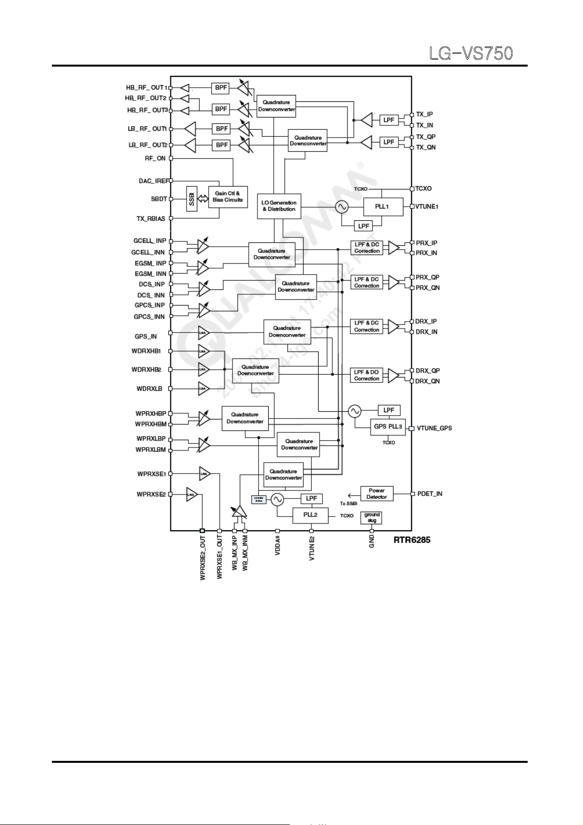
[Figure 1.7] RTR6285 IC Functional Block Diagram
1.4. LO GENERATION and DISTRIBUTION CIRCUIT
The integrated LO generation and distribution circuits are driven by internal VCOs to support
various modes to yield highly flexible quadrature LO outputs that drive all GSM/EDGE,
UMTS band and GPS upconverters and downconverters; with the help of these LO generation
and distribution circuits, true zero-IF architecture is employed in all GSM and UMTS band
receivers and transmitters to translate the signal directly from RF-to-baseband and from
baseband-to-RF. Two fully functional fraction-N synthesizers, including VCOs and loop
filters, are integrated within the RTR6285 IC. In addition, the RTR6285 has a third
- 16 -
LG-VS750
- 17 -
synthesizer used for GPS operation. The first synthesizer (PLL1) in the RTR6285 creates the
transceiver Los that support the UMTS transmitter, and all four GSM band receivers and
transmitters including: GSM850, GSM900, GSM1800, and GSM1900. The second
synthesizer (PLL2) in the RTR6285 IC provides the LO for the UMTS primary receiver. For
the RTR6285 IC only, the second synthesizer also provides the LO for the secondary UMTS
receiver. The third synthesizer (PLL3), only in the RTR6285 IC, provides the LO for the GPS
receiver. An external TCXO input signal is required to provide the synthesizer frequency
reference to which the PLL is phase and frequency locked. The RTR6285 ICs integrate most
of the PLL loop filter components on-chip except for three off-chip loop filter-series
capacitors, which significantly reduces off-chip component requirement. With the integrated
fractional-N PLL synthesizers, the RTR6285 ICs have the advantage of more flexible loop
bandwidth control, fast lock time, and low-integrated phase error.
1.5. OFF-CHIP RF COMPONENTS
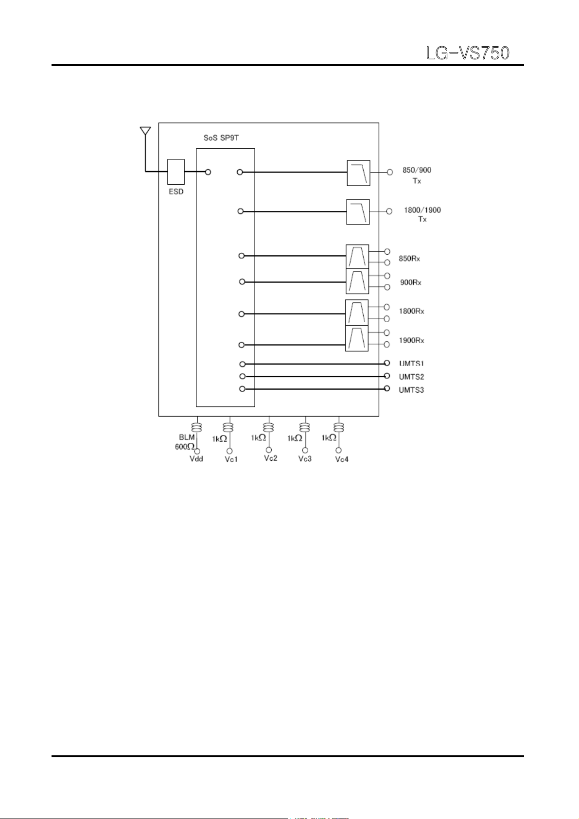
1.5.1 LMSP43QL-771(F1001: FEM, Front End Module)
Application
Low-loss SAW front-end module for mobile telephone system
Covering GSM850, GSM900, GSM1800, GSM1900, WCDMA 2100 bands
Integration fo TX low pass filters, switches and decoder
Integration of GSM 850, EGSM, PCN and PCS RX SAWs
Balanced outputs of all RX ports
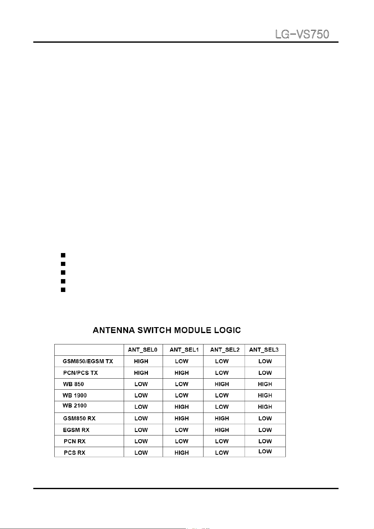
[Table 1] Antenna Switch Module Logic
LG-VS750
- 18 -
[Figure 1.8] LMSP43QL-771 Functional Block Diagram.
1.5.2 W-CDMA 1900 POWER AMPLIFIER (U1019: ACPM-5202)
The ACPM-5202 is fully matched 10-pin surface mount module developed for UMTS Bnad2.
This power amplifier module operates in the 1850-1910MHz bandwidth. The ACPM-5202
meets stringent UMTS linearity requirements up to 28dBm output power (Rel99). The 3mm x
3mm form factor package is self contained, incorporation 50ohm input and output matching
networks.
th
The ACPM-5202 features 5
generation of CoolPAM circuit technology which supports 3
power modes-bypass, mid and high power modes. The CoolPAM is stage bypass technology
enhancing PAE (power added efficiency) at low and medium power range. Active bypass
feature is added to 5
th
generation to enhance PAE further at low output range. This helps to
extend talk time. A directional coupler is integrated into the module and both coupling and
isolation ports are available externally, supporting daisy chain.
LG-VS750
- 19 -
[Figure 1.9] ACPM-5202 Amplifier module features
1.5.3 WCDMA 2100 POWER AMPLIFIER (U1024: ACPM-5201)
The ACPM-5201 is fully matched 10-pin surface mount module developed for UMTS Bnad1.
This power amplifier module operates in the 1920-1980MHz bandwidth. The ACPM-5201
meets stringent UMTS linearity requirements up to 27.5dBm output power (Rel99). The 3mm
x 3mm form factor package is self contained, incorporation 50ohm input and output matching
networks.
The power amplifier is manufactured on an advanced InGaP HBT (hetero-junction Bipolar
Transistor) MMIC (microwave monolithic integrated circuit) technology offering state-of-theart reliability ,temperature stability and ruggedness.
[Figure 1.10] ACPM-5201 Amplifier module features
LG-VS750
- 20 -
1.5.4 WCDMA 900 POWER AMPLIFIER (U1023: ACPM-5308)
The ACPM-5308 is fully matched 10-pin surface mount module developed for UMTS EGSM.
This power amplifier module operates in the 880-915MHz bandwidth. The ACPM-5308
meets stringent UMTS linearity requirements up to 28dBm output power (Rel99). The 3mm x
3mm form factor package is self contained, incorporation 50ohm input and output matching
networks.
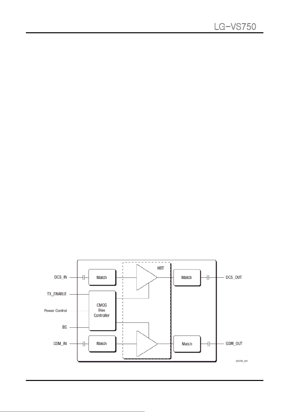
1.5.5 Quad-Band GSM/EDGE Polar Power Amplifier Module (U1007: SKY77336)
SKY77336 Power Amplifier Module (PAM) is designed in a compact form factor for quadband cellular handsets comprising GSM850/900, DCS1800 and PCS1900, supporting
Gaussian Minimum-Shift Keying(GMSK) and Polar Enhanced Data for GSM Evolution
(EDGE) modulation. Class 12 General Packet Radio Service (GPRS) multi-slot operation is
also supported.
The module consists of GSM850/900 PA and DCS1800/PCS1900 PA blocks, impedance
matching circuitry for 50 Ω input and output impedances, and a Power Amplifier Control
(PAC) block. The custom CMOS integrated circuit provides the internal PAC function and
interface circuitry. Fabricated in InGaP/GaAs, the heterojunction Bipolar Transistor (HBT) PA
blocks support the GSM850/900 bands and DCS1800/PCS1900 bands. Both PA blocks share
common power supply pads to distribute current. The InGaP/GaAs die, Silicon (Si) controller
and passive components are mounted on a multi-layer laminate substrate and the entire
die,
assembly is encapsulated with plastic overmold.
RF input and output ports of the SKY77336 are internally matched to a 50 Ω load to reduce
the number of external components for a quad-band design.Extremely low leakage current (10
μA, typical) of the PAM module maximizes handset standby time.
The SKY77336 also contains band-select switching circuitry to select GSM(logic 0) or
DCS/PCS (logic 1) as determined from the Band Select (BS) signal. See Figure 1.11 shown
below.
[Figure 1.11] SKY77336 Functional Block Diagram.
1. TROUBLE SHOOTING
- 21 -
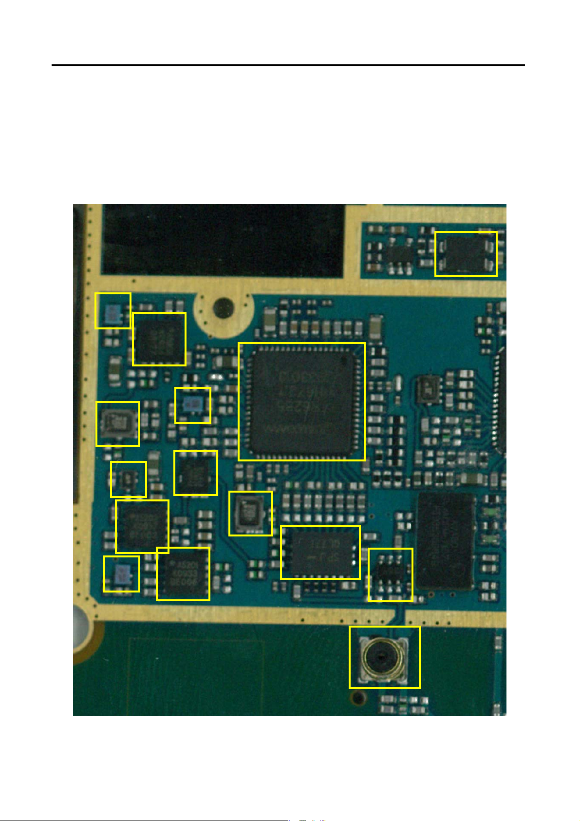
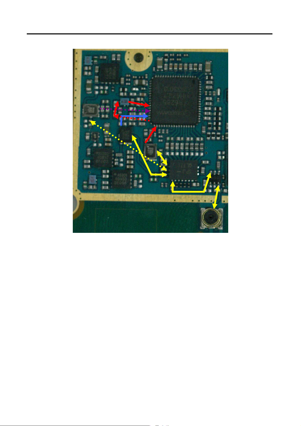
1.1 RF Component
F1008
1.TROUBLE SHOOTING
U1013
U1023
DP1003
F1009
U1019
F1003
F1006
DP1500
U1024
U1011
DP1000
F1001
SW1000

1.TROUBLE SHOOTING
- 22 -
U1007
RF component (WCDMA / GSM)
Reference Description Reference Description
U1011 RTR6285(Transceiver) F1008 WCDMA (VIII) Tx SAW Filter
U1007 GSM / EDGE PAM F1003 WCDMA (I) Tx SAW Filter
U1024 WCDMA Single (I) PAM DP1000 WCDMA (I) Duplexer
U1019 WCDMA Single (II) PAM DP1500 WCDMA (II) Duplexer
U1023 WCDMA Single (VIII) PAM F1009 WCDMA (II) Tx SAW Filter
F1001 Front End Module F1006 WCDMA (I) Rx SAW Filter
U1021 SPDT U1013 VCTCXO (19.2MHz)
DP1003 WCDMA (VIII) Duplexer U1000 RF Antenna Connector
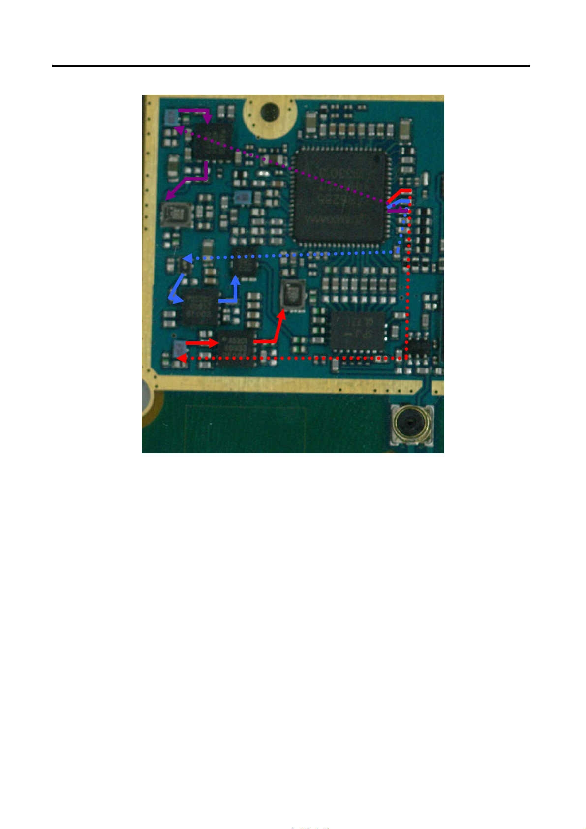
1.2 SIGNAL PATH
- 23 -
1.TROUBLE SHOOTING
GSM850/GSM900/DCS/PCS’s RX/TX Signal PATH
A. GSM850/GSM900/DCS1800/PCS1900 RX PATH
B. GSM850/GSM900/DCS1800/PCS1900 TX PATH
C. COMMON TX/RX PATH
1.TROUBLE SHOOTING
- 24 -
WCDMA BAND I, II & VIII RX Signal PATH
D1. WCDMA 2100 RX PATH
E1. WCDMA 1900 RX PATH
F1. W900 Rx PATH
G1. COMMON TX/RX PATH
1.TROUBLE SHOOTING
- 25 -
WCDMA I,II and VIII Band TX Signal PATH
D2. WCDMA 2100 TX PATH
E2. WCDMA 1900 TX PATH
F2. W900 Rx PATH
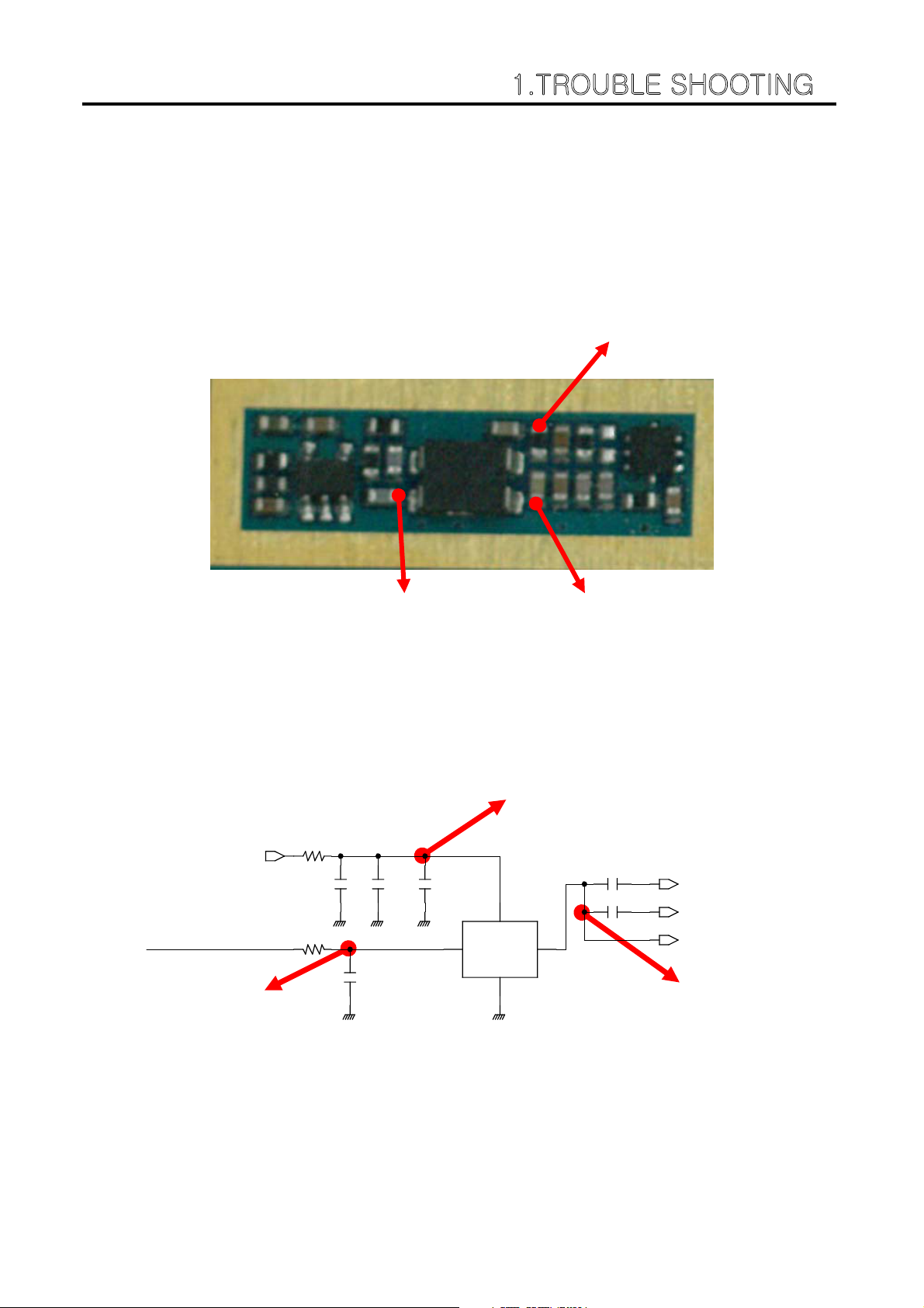
1.TROUBLE SHOOTING
C1127
10n
C1125
0.1u
R1046
100
TCXO_PMIC
C1220
100p
C1256
33p
C1126
10n
C1171
100p
R1045
51
TCXO
+2.85V_TCXO
TCXO_USB
TG-5010LH_19_2M-75A
U1013
1
VC
2
GND
3
OUT
4
VCC
VCTCXO(19.2 MHz)
- 26 -
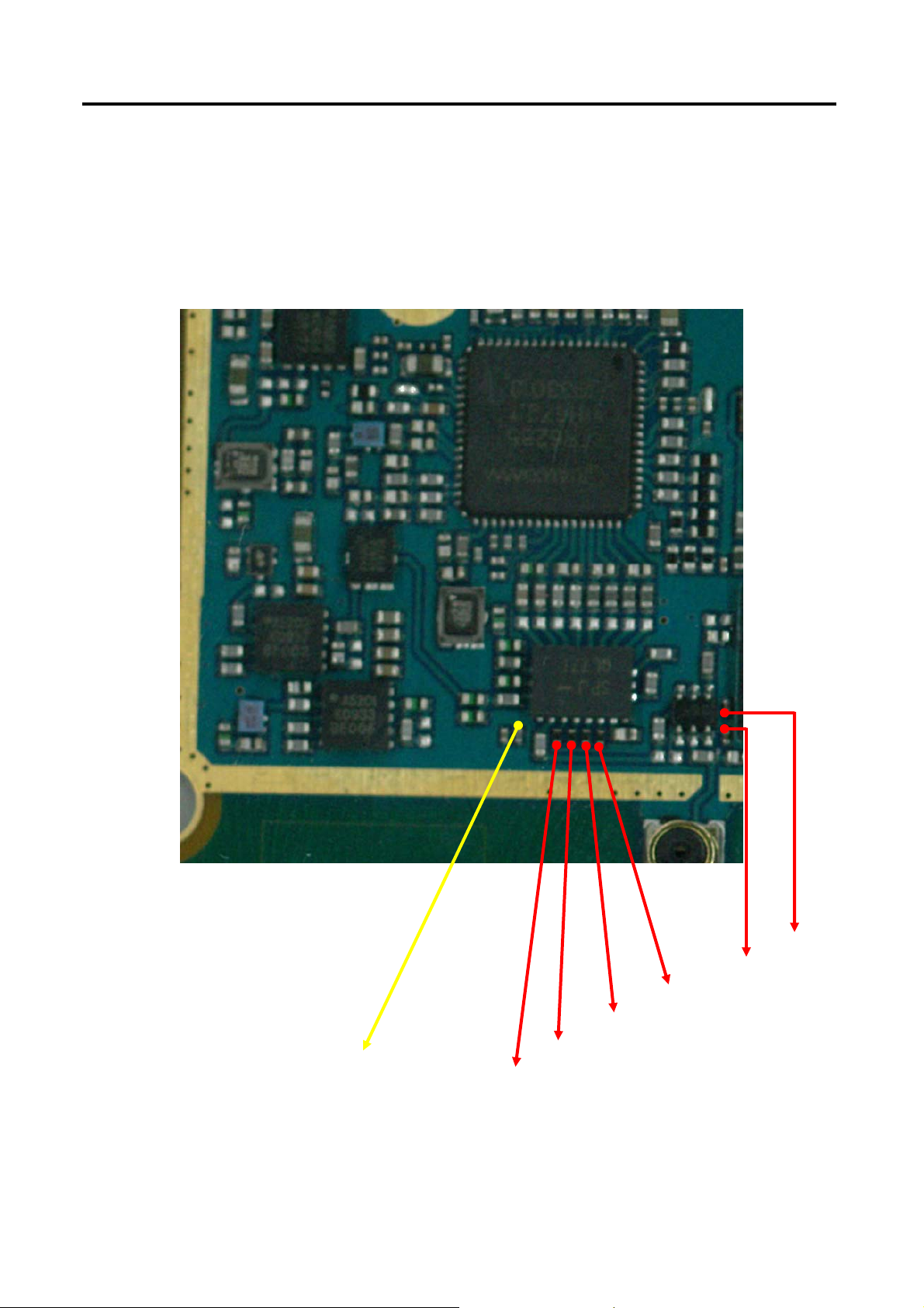
1.3 Checking TCXO Block
The output frequency (19.2MHz) of TCXO (X300) is used as the reference one of RTR6285
and PM7540 internal VCO.
TP1
TP3
TP2
TP1
TP2
Schematic of the Crystal Part (19.2MHz)
TP3
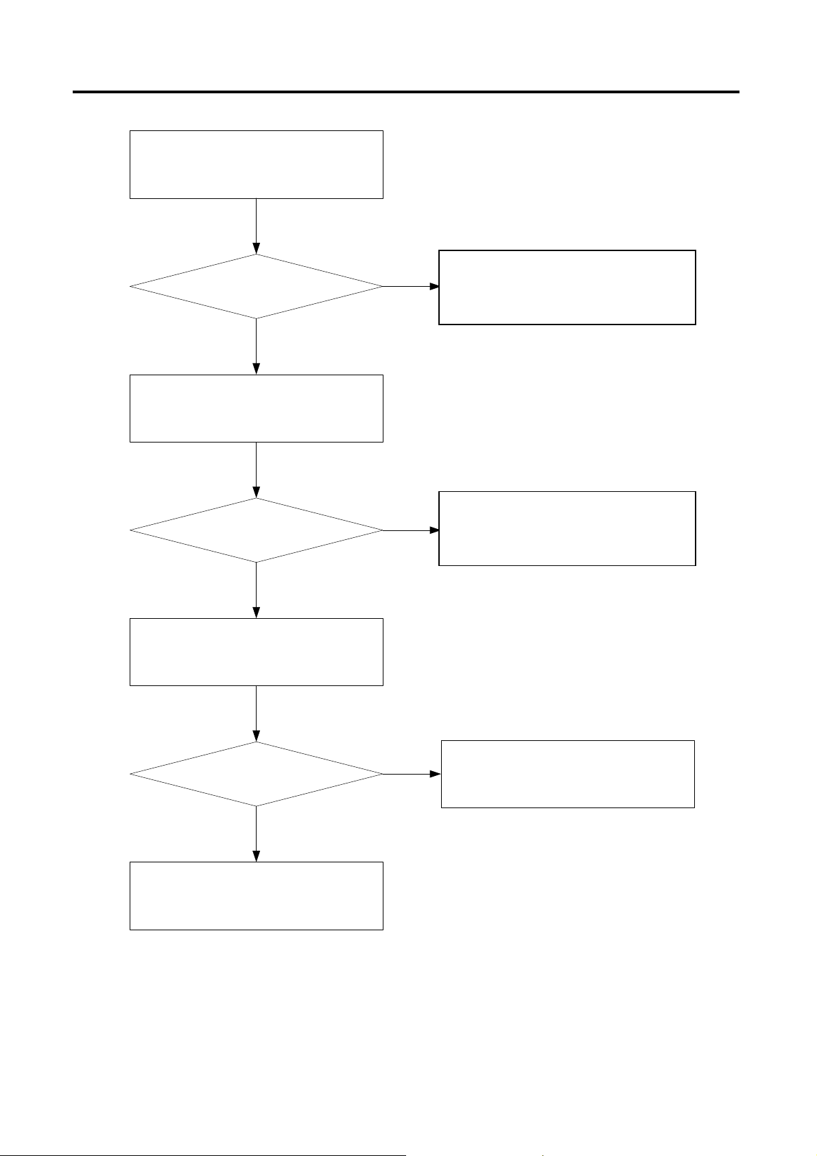
Check TP1
- 27 -
VCC of TCXO
VCC ≥ 2.8 V
Yes
Check TP2
No
1.TROUBLE SHOOTING
Check PM6658
Check the PM7540
2.4V ≥ Voltage ≥ 0.4V
Yes
Check TP3
19.2 MHz Signal
Yes
TCXO is OK
No
No
Check MSM6280
Check the QSD8650
Check soldering and
components
1.4 Checking FEM Block
- 28 -
1.TROUBLE SHOOTING
CTRL6
CTRL5
+2.85V_SYNTH
CTRL4
CTRL3
CTRL2
CTRL1
 Loading...