

Page 1

PDP MODULE
English
SERVICE MANUAL
MODEL : PDP42V7####
CAUTION
1. BEFORE SERVICING THE PDP MODULE,
READ THE SAFETY PRECAUTIONS IN THIS MANUAL.
2. WHEN REPLACEMENT PARTS ARE REQUIRED, BE SURE TO USE
REPLACEMENT PARTS SPECIFIED BY THE MANUFACTURER.
Page 2

- 2 -
[PDP42V7#### Module]
CONTENTS
Ⅰ. Safety Precautions/Technical Feature
Ⅱ. Formation and Specification of Module
Ⅲ. Adjustment
Ⅳ. Trouble Shooting
1. Checking for No Picture
2. Hitch Diagnosis Following Display Condition
2-1. All or 1/2 of the screen doesn’t be shown
2-2. Screen doesn’t be shown as Data TCP
2-3. It is generated unusual pattern of Data TCP IC unit
2-4. Regular Stripe is generated about the quantity of one Data TCP IC or more
2-5. Screen doesn’t be shown at all as Scan FPC
2-6. Regular stripe is generated at regular internal on the whole screen
2-7. Data copy is generated to stripe direction
2-8. One or more stripe is generated on the screen
2-9. One or more horizontal line is generated on screen
2-10. Lightness of screen is wholly darken though there is input-signal-pattern
2-11. Different color is shown partially during full-white-screen or electric discharge is generated
during full-black-screen
2-12. Some lightness of some color doesn’t not generated well
3. Checking for component damage
3-1. Y IPM(IC15) or Z IPM(IC2) damage
3-2. Pass Top FET(Y B/D: HS2) damage
3-3. FET Ass’y(Y B/D: HS1) damage
3-4. SCAN IC(Y DRV B/D: IC1~8) damage
3-5. TCP damage
3-6. Crystal(CTRL B/D: X1) damage
4. Shift breakdown component compatibility consideration
4-1. Scan IC follows in application, compatibility of Y DRV Top, Bottom B/D
Ⅴ. Block Diagram
Ⅵ. Safety Components List
Ⅶ. Records of Revision for Boards, Components and ROM DATA
* Annexing : Schematic Diagram
Page 3

English
- 3 -
1. Safety Precautions
When servicing of PDP Module, it should be not enforced into
another way aside next rule, or a unaccustomed person
should not repairing.
When using/handling this PDP Module, pay attention to the
below warning and cautions.
Warning
Indicates a hazard that may lead to death or injury if the
warning is ignored and the product is handled incorrectly.
Caution
Indicates a hazard that can lead to injury or damage to
property if the caution is ignored and the product is handled
incorrectly.
1) WARNING
(1) Do not touch Signal and Power Connnector while this
product operates.
Do not touch EMI ground part and Heat Sink of Film Filter.
(2) Do not supply a voltage higher than that specified to this
product. This may damage the product and may cause a
fire.
(3) Do not use this product in locations where the humidity is
extremely high, where it may be splashed with water, or
where flammable materials surround it.
Do not install or use the product in a location that does no
satisfy the specified environmental conditions. This may
damage the product and may cause a fire.
(4) If a foreign substance (such as water, metal, or liquid) gets
inside the product, immediately turn off the power.
Continuing to use the product, it is may cause fire or
electric shock.
(5) If the product emits smoke, and abnormal smell, or makes
an abnormal sound, immediately turn off the power.
Continuing to use the product, it may cause fire or electric
shock.
(6) Do not disconnect or connect the connector while power to
the product is on. It takes some time for the voltage to drop
to a sufficiently low level after the power has been turned
off.
Confirm that the voltage has dropped to a safe level before
disconnecting or connecting the connector.
(7) Do not pull out or insert the power cable from/to an outlet
with wet hands. It may cause electric shock.
(8) Do not damage or modify the power cable. It may cause
fire or electric shock.
(9) If the power cable is damaged, or if the connector is loose,
do not use the product: otherwise, this can lead to fire or
electric shock.
(10) If the power connector or the connector of the power
cable becomes dirty or dusty, wipe it with a dry cloth.
Otherwise, this can lead to fire.
(11) PDP Module uses a high voltage (Max.450V dc). Keep
the cautions concerning electric shock and do not touch
the Device circuitry when handling the PDP Unit. And
because the capacitor of the Device circuitry may remain
charged at the moment of Power OFF, standing by for 1
minute is required in order to touch the Device circuitry.
2) CAUTIONS
(1) Do not place this product in a location that is subject to
heavy vibration, or on an unstable surface such as an
inclined surface. The product may fall off or fall over,
causing injuries.
(2) Before disconnecting cable from the product, be sure to
turn off the power. Be sure to hold the connector when
disconnecting cables. Pulling a cable with excessive force
may cause the core of the cable to be exposed or break
the cable, and this can lead to fire or electric shock.
(3) This product should be moved by two or more persons. If
one person attempts to carry this product alone, he/she
may be injured.
(4) This product contains glass. The glass may break, causing
injuries, if shock, vibration, heat, or distortion is applied to
the product.
(5) The temperature of the glass of the display may rise to
80°C or more depending on the conditions of use.
If you touch the glass inadvertently, you may be burned.
(6) If glass surface of the display breaks or is scratched, do
not touch the broken pieces or the scratches with bare
hands. You may be injured.
(7) PDP Module requires to be handled with care not to be
touched with metal or hard materials, and must not be
stressed by heat or mechanical impact.
(8) There are some exposed components on the rear panel of
this product. Touching these components may cause an
electric shock.
(9) When moving the product, be sure to turn off the power
and disconnect all the cables. While moving the product,
watch your step. The product may be dropped or all,
leading to injuries of electric shock.
Ⅰ. Safety Precautions/Technical Feature
Page 4

(10) In order to protect static electricity due to C-MOS circuitry of
the Drive part, wear a wrist band to protect static electricity
when handling.
(11) If cleaning the Panel, wipe it with a soft cloth moistened with
water or a neutral detergent and squeezed, being careful not
to touch the connector part of the Panel. And don’t use
chemical materials like thinner or benzene.
(12) If this product is used as a display board to display a static
image, “image sticking” occurs. This means that the luminance
of areas of the display that remain lit for a long time drops
compared with luminance of areas that are lit for a shorter
time, causing uneven luminance across the display.
The degree to which this occurs is in proportion to the
luminance at which the display is used. To prevent this
phenomenon, therefore, avoid static images as much as
possible and design your system so that it is used at a low
luminance, by reducing signal level difference between bright
area and less bright area through signal processing.
(13) Because PDP Module emits heat from the Glass Panel part
and the Drive circuitry, the environmental temperature must
not be over 40°C.
The temperature of the Glass Panel part is especially high
owing to heat from internal Drive circuitry. And because the
PDP Module is driven by high voltage, it must avoid
conductive materials.
(14) If inserting components or circuit board in order to repair, be
sure to fix a lead line to the connector before soldering.
(15) If inserting high-power resistor(metal-oxide film resistor or
metal film resistor) in order to repair, insert it as 10mm away
as from a board.
(16) During repairs, high voltage or high temperature components
must be put away from a lead line.
(17) This is a Cold Chassis but you had better use a cold
transformer for safety during repairs. If repairing electricity
source part, you must use the cold transformer.
(18) Do not place an object on the glass surface of the display.
The glass may break or be scratched.
(19) This product may be damaged if it is subject to excessive
stresses (such as excessive voltage, current, or temperature).
The absolute maximum ratings specify the limits of these
stresses.
(20) The recommended operating conditions are conditions in
which the normal operation of this product is guaranteed. All
the rated values of the electrical specifications are guaranteed
within these conditions.
Always use the product within the range of the recommended
operating conditions. Otherwise, the reliability of the product
may be degraded.
(21) This product has a glass display surface. Design your
system so that excessive shock and load are not applied to
the glass. Exercise care that the vent at the corner of the glass
panel is not damaged.
If the glass panel or vent is damaged, the product is
inoperable.
(22) Do not cover or wrap the product with a cloth or other
covering while power is supplied to the product.
(23) Before turning on power to the product, check the wiring of
the product and confirm that the supply voltage is within the
rated voltage range. If the wiring is wrong or if a voltage
outside the rated range is applied, the product may
malfunction or be damaged.
(24) Do not store this product in a location where temperature
and humidity are high. This may cause the product to
malfunction. Because this product uses a discharge
phenomenon, it may take time to light (operation may be
delayed) when the product is used after it has been stored for
a long time. In this case, it is recommended to light all cells for
about 2 hours (aging).
(25) This product is made from various materials such as glass,
metal, and plastic. When discarding it, be sure to contact a
professional waste disposal operator.
(26) If faults occur due to arbitrary modification or disassembly,
LG Electronics is not responsible for function, quality or other
items.
(27) Use of the product with a combination of parameters,
conditions, or logic not specified in the specifications of this
product is not guaranteed. If intending to use the product in
such a way, be sure to consult LGE in advance.
(28) Within the warranty period, general faults that occur due to
defects in components such as ICs will be rectified by LGE
without charge. However, IMAGE STICKING due to
misapplying the above (12) provision is not included in the
warranty. Repairs due to the other faults may be charged for
depending on responsibility for the faults.
(29) In assembling Module into SET, in case Film Filter and as a
protective film is bared, static electricity of exfoliated protective
film which is bared from beginning X-Board down ward getting
TCP to no getting TCP should not influence on TCP.
Also Filter after protective film is bared or in the storage can
be charged with electricity, so the EMI ground part of Film
Filter should be used after Grounding.
- 4 -
Page 5
English
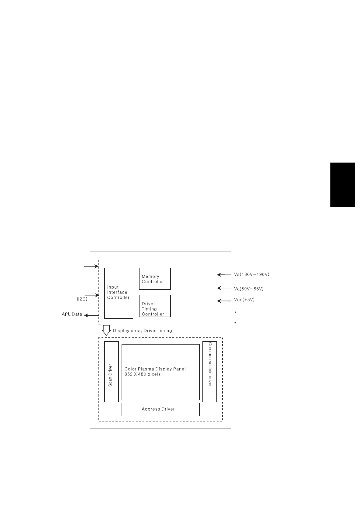
2. Technical Feature
PDP Module is a display device to be divided into a Panel part and a Drive part. The Panel part consists of
Electrodes, Phosphor, various dielectrics and gas, and the Drive part includes electronic circuitry and PCB.
PDP42V7#### model produced in the LG electronic is 42inches color Plasma display module of WVGA(852(H)x480(V)), and it is a
display device giving concrete to bright image by using AC Plasma technology of LG electronic.
1) General Specification
(1) Model Name : PDP42V7####
(2) Number of Pixel : 852(H) x 480(V) (1pixel=3 RGB cells)
(3) Pixel Pitch : 1080μm(H) x 1080μm(V)
(4) Cell Pitch : 320μm(H) x 1080μm(V) (Base: Green Cell)
(5) Display area : 920.1(H) x 518.4(V)±0.5mm
(6) Outline dimension : 1005(H) x 597(V)x 60.6(D)±1mm
(7) Color arrangement : RGB Closed type
(8) Number of COLRO : (R)1024 x (G)1024 x (B)1024
(9) Weight : 14.7Kg±0.5Kg
: 100Kg±5Kg(5EA/1BOX)
(10) Aspect Ratio : 16:9
(11) Peak Brightness : Typical 1500dc/㎡(1/10 White Window)
: Avergae 100:1(Light room 100 Lx at center)
(12) Contrast Ratio : Typical 10000:1(Dark room 1/10 White Window)
(White Window Pattern at Center)
(13) POWER CONSUMPTION : Typical 200 W(Full White)
* Note 1)
(14) Lifetime : Over 60,000 Hrs (Initial brightness 1/2)
2) Block Diagram
- 5 -
LVDS Input
Controller Signal
Full White standard
Mentioned voltage follows
a standard of each Board input voltage
* Note 1) It can be changed maximum 300W according to input image.
Page 6
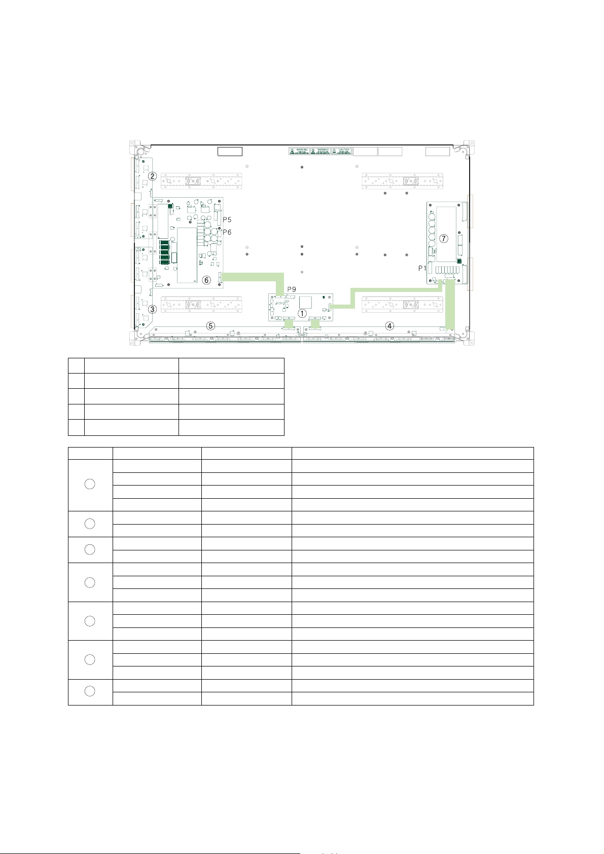
Ⅱ. Formation and Specification of Module
- 6 -
No
1
2
3
4
Connector
P1[Z SUS B/D]
P5[Y SUS B/D]
P6[Y SUS B/D]
P9[CTRL B/D]
Input Voltage & Signal
5V, Va, Vs
Vs
5V
Control Signal
No
1
2
3
4
5
6
7
6871QCH053A
6871QCH073A
6871QCH053B
6871QCH053C
6871QDH084A
6871QDH105A
6871QDH085A
6871QDH106A
6871QRH055A
6871QRH055B
6871QRH066A
6871QLH047A
6871QLH047B
6871QLH056A
6871QYH036A
6871QYH036B
6871QYH050A
6871QZH041A
6871QZH052A
PWB(PCB) ASS’Y
PWB(PCB) ASS’Y
PWB(PCB) ASS’Y
PWB(PCB) ASS’Y
PWB(PCB) ASS’Y
PWB(PCB) ASS’Y
PWB(PCB) ASS’Y
PWB(PCB) ASS’Y
PWB(PCB) ASS’Y
PWB(PCB) ASS’Y
PWB(PCB) ASS’Y
PWB(PCB) ASS’Y
PWB(PCB) ASS’Y
PWB(PCB) ASS’Y
PWB(PCB) ASS’Y
PWB(PCB) ASS’Y
PWB(PCB) ASS’Y
PWB(PCB) ASS’Y
PWB(PCB) ASS’Y
LVDS CTRL B/D ASS’Y
HITACHI COPPER LVDS CTRL B/D ASS’Y
LVDS OUTER SIDE CTRL B/D ASS’Y
PB-FREE FFC & CON LVDS OUTER SIDE CTRL B/D ASS’Y
YDRV TOP B/D ASS’Y
HITACHI COPPER YDRV TOP B/D ASS’Y
YDRV BTM B/D ASS’Y
HITACHI COPPER YDRV BTM B/D ASS’Y
XR B/D ASS’Y
PB-FREE FFC & CON XR B/D ASS’Y
HITACHI COPPER XR B/D ASS’Y
XL B/D ASS’Y
PB-FREE FFC & CON XL B/D ASS’Y
HITACHI COPPER XL B/D ASS’Y
YSUS B/D ASS’Y
PB-FREE FFC & CON YSUS B/D ASS’Y
HITACHI COPPER YSUS B/D ASS’Y
ZSUS B/D ASS’Y
HITACHI COPPER ZSUS B/D ASS’Y
Part No. Description
※ The composition and specification of Initial production module
Revision information refers to ‘Ⅶ Revision for Boards, Components and ROM DATA’
Page 7
Ⅲ. Adjustment
1. Application Object
This standard is applied to the PDP42V7#### PDP Module
which is manufactured by the manufacturing team of PDP
promotion department or elsewhere.
2. Notes
(1) Without any special specification, the Module should be at
the condition of preliminaries more than 10minutes before
adjusting.
- Service signal : 100% Full White signal
- Service DC voltage : Vcc: 5V, Va: 65V, Vs: 187V
- DC/DC Pack voltage : Vsc=115V
- Preliminaries environment : Temp (25!5°C), Relative
humidity (65!10%)
(2) Module should get the Aging for the equilibrium after finish
the assembling. Aging condition is shown below.
- Service signal: 100% Full White, Red, Green, Blue pattern
signal(Service time of each pattern : within 5minutes/cycle)
- Service DC voltage : Match the voltage with the set up
voltage in the first adjustment.
- Aging time : More than 30 minutes
- Aging environment : Temp (25!2°C), Relative humidityLess than 65%
(3) Module adjustment should be followed by below sequence.
- Setting up the Vsc/-Vy voltage(Vsc=115V, -Vy=-85V)
-
Adjusting the voltage wave form(Refer to adjustment)
-
25!5°C, 65!10%
(4) Without any special specification, you should adjust the
Module in the environment of Temp (25!5°C) and Relative
humidity (65!10%)
Caution) If you let the still image more than 10 minutes(especially
The Digital pattern or Cross Hatch Pattern which has
clear gradation), after image can be presented in the
black level part of screen.
-Vy: -85V
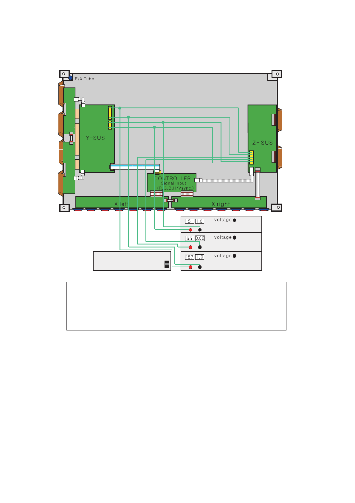
3-2. Connection diagram of measuring
instrument and setting up the initial
voltage
(1) For connection diagram of measuring instrument,
refer to Fig. 1.(Connection diagram of measuring
instrument that adjusting the voltage wave form)
(2) Setting up the initial voltage(Voltage Label)
Vcc: 5V, Va: 65V, Vs: 187V
But, Initially setting up voltage can be changed by the set
up range according to the Module’s characteristic.
3-3. How to Adjust
(1) Adjusting Vset-up Voltage Wave form
① Connect the measuring instrument to be (Fig. 1).
② Turn on the measuring instrument with Caution of (Fig. 1).
③ Connect the oscilloscope probe to B39(Bead) of Y B/D
bottom and GND.
④ Turn the VR1 of Y B/D and make the “A“ waveform Fig.
2 to be 10!2µs.
(2) Adjusting Vset-down Voltage Wave form
① Turn the VR2 of YSUS B/D and make the “B“ waveform
Fig. 2 to be 100!2µs.
English
3. Adjustment after Assembling
3-1. Using Tools
(1) Digital oscilloscope : More than 200MHz
(2) DVM(Digital Multimeter) : Fluke 87 or similar one
(3) Signal generator : VG-825 or similar one
(4) DC power supply or PSU
- DC power supply for Vs (1) : Should be changeable
between 0V to 200V/ more than 10A
- DC power supply for Va (1) : Should be changeable
between 0V to 100V/ more than 5A
- DC power supply for 5V (1) :Should be changeable
between 0V to 10V/ more than 10A
- DC-DC Converter Jig (1) : The Jig which has equivalent
voltage output of PDP42V7#### Module after taking the
Vs, Va, 5V voltage
- Voltage stability of power supply : Within !1% for Vs/Va,
within !3% for 5V
(Fig. 2) Y, Z set-up Waveform
(3) Checking the DC/DC pack voltage
① Convert the signal of signal generator to the 100% Full
White signal.
② Connect the GND terminal of DVM to the right leg of R53
on the Y B/D and set the Plus terminal to the left leg of
R53 to check the Vsc voltage(115!1V) and when there is
abnormality in voltage turn the variable resistor(VR3) of
DC/DC Pack(Vsc) PS1 on Y B/D to adjust.
③ Connect the GND terminal of DVM to the right leg of
R78 on the Y B/D and set the Plus terminal to the left
leg of R78 to check the -Vy voltage(-85!1V) and when
there is abnormality in voltage turn the variable
resistor(VR4) of DC/DC Pack(-Vy) PS1 on Y B/D to
adjust.
- 7 -
Page 8
- 8 -
<Caution>
(1) The power of the signal generator should be turned on before turning on the power of DC power supply.
(2) The voltage of DC power supply , in standard of Module input voltage, should be preset as below.
Vcc: 5V, Va: 65V, Vs: 187V
(3) The power of power supply must turned on by this sequence. Reverse direction When turning off.
* Module on : 5V
(Va(
Vs, Module off: Vs(Va(5V
(4) Signal generator should be selected with 852)480(WVGA) mode.
(Fig. 1) Connection diagram of measuring instrument
DC Power Supply for 5V
DC Power Supply for Va
DC Power Supply for Vs
Power
Signal Generator(VG-825)
※ Also the PSU(Power Supply Unit) use is possible
Page 9

1. Checking for no Picture
A screen doesn’t display at all and condition of black pattern or power off.
(1) Check whether the CTRL B/D LED(D1, D2, D3, D4, D5) is turned on or not.
(2) Check the power and signal cable of CTRL B/D.
(3) X B/D, Y B/D, Z B/D is well plugged in.
(4) Check the connection of X B/D, Y B/D and Z B/D to CTRL B/D.
(5) Measure the output wave of X, Y, Z B/D with oscilloscope(more than 200MHz)
and find the trouble of B/D by comparing the output wave with below figure.
- Measure Point fo Y B/D : Bead B39
- Measure Point fo Z B/D : Bead B28
- Measure Point fo X B/D : P3
(6) Check the SCAN(Y side) IC
(7) Check the DATA(X side) TCP IC
(8) Replace the CTRL B/D.
(9) Check the Fuse of Y, Z B/D is open and replace when open.
(10) Check the input voltage. (Vcc=5V/Va=65V/Vs=187V)
English
- 9 -
Ⅳ. Trouble Shooting
Y B/D Output wave (1frame)
Z B/D Output wave (1frame)
Page 10

- 10 -
Y B/D Output wave(1SF)
Z B/D Output wave(1SF)
X B/D Output wave(1frame): Va measurement
Page 11

English
2. Hitch Diagnosis Following
Display Condition
2-1. All or 1/2 of the screen doesn’t be shown
(1) In case of all of the screen doesn’t be shown, Confirm the
8pin connection of X B/D to Z B/D is well plugged in which
is correspond
(2) In case of 1/2 of the screen doesn’t be shown
①
XR B/D
- Confirm the 60pin connection of CTRL B/D to XR B/D
is well plugged in which is correspond
②
XL B/D
- Confirm the 5pin connection of XR B/D to XL B/D is
well plugged in which is correspond
- Confirm the 60pin connection of CTRL B/D to XL B/D
is well plugged in which is correspond
(3) Replace relevant X B/D.
[[
Relationship between screen and X B/D
Screen X B/D
Left of the Screen 1/2 <--> Right X B/D
Right of the Screen 1/2 <--> Left X B/D
[[
Screen Display Form
[[
1/4 of the screen doesn’t be shown
Equality with 2-1
2-2. The screen doesn’t be shown as Data
TCP
(Include not be shown part of DataTCP quantity or a part)
(1) The problem between Data TCP and X B/D is more
possible that the screen is not be shown as data TCP.
(2) Confirm the connector of Data TCP is well connected to X
B/D. Correspond to the part that screen is not showing
(3) Confirm whether the Data TCP is failed.
(Inclusion examination with the naked eye(IC Burnt and
others)
①
IC is Fail: Replace the Module
②
In case of shorting the X B/D by foreign or PCB pattern
is open: When TCP IC is not Fail, replace the X B/D.
[[
Example of the screen display form
(Anything of the 14 Data TCP can be shown beside below
pictures)
- 11 -
Left of the Screen(1/2) Right of the Screen(1/2)
Display
Not display
: All
: Partial
: not at all
[[
How to examine Data TCP IC
● Change ‘①(Va Power)‘ into CATHOD, ‘②(GND)‘ into
ANODE and then examine the Diode to the forward
or reverse direction.
● Burnt of ‘③(IC)’ and others examine with the naked
eye.
Page 12

2-3. It Generates Unusual Pattern of Data
TCP IC unit
(1) In case of generating unusual pattern of Data TCP IC unit
as below picture, there is problem in the Signal(CLK, data,
STB) or connector that is input into Data TCP IC
(2) In case of <case 1>
- Confirm the connection of Data TCP connector and IC
Fail.
- Replace the relevant X B/D.
(3) In case of <case 2>, <case 3>
- Confirm the connection of Data TCP connector and
connector that is connected from CTRL to X B/D.
- Check the foreign on the CTRL B/D and X B/D.
- Replace the relevant X B/D or CTRL B/D.
(4) In case of <case 4>, <case 5>
- Confirm the connector that is connected from CTRL to X B/D
- Replace relevant X B/D or CTRL B/D
- Confirm the connection of Z B/D and XR B/D(8pin), XR
B/D and XL B/D(5pin) power connector.
[[
Screen Display Form
2-4. Regular Stripe is Generated about the
Quantity of one Data TCP IC or more
(1) In case of generating regular stripe about the quantity of one
Data TCP IC or more, check the connection of connector or
foreign.
(2) Confirm the connection connector/foreign of XB/D or CTRL
B/D to X B/D correspond to unusual screen.
(3) Replace relevant XB/D or CTRL B/D.
[[
Screen Display Form
- 12 -
<Case 1>
Unusual screen comes
out about one TCP IC
quantity or more
Unusual screen comes
out about 1/2 of screen
or equal distances of
all screen
Unusual screen comes
out about 4/14 quantity
of screen or 3/14
Unusual screen comes
out about 1/2 quantity
of screen
Unusual screen comes
out about all screen
<Case 2>
<Case 3>
<Case 4>
<Case 5>
It comes out partial field about
the quantity of one IC or more
or It may come out together
at other field of screen.
Page 13

English
- 13 -
2-5. The screen display has a problem for
Scan FPC.
(1) It’s may be a problem between Scan FPC and Y DRV B/D.
(2) Check the connection of Y DRV B/D and Scan FPC.
(3) If the Scan IC is failed, replace the Y DRV B/D.
[[
Screen Display Form
[[
Check a method of SCAN IC
Change the Vpp Pin into ANODE and GND Pin into CATHOD
and then test the Diode with forward or reverse direction.
2-6. The screen has a vertical line with
regular gap.
(A vertical stripe flash at especial color)
(1) This is a problem about CTRL B/D.
(2) Replace the CTRL B/D.
[[
Screen Display Form
2-7. A data copy is happened into vertical
direction
(1) In this case, it’s due to incorrect marking of scan wave.
(2) Replace the Y DRV B/D or Y B/D.
[[
Screen Display Form
one eighth
of screen
The screen display is very good
The screen display is poor
The screen has a vertical line
with regular gap
<Case 1 : Entire Copy><Display Pattern>
<Case 2 : Top Copy>
<Case 3 : Bottom Copy> <Case 4 : Entire Copy>
Page 14

- 14 -
2-8. The screen has one or several vertical
line
(1) In this case, It isn’t a problem about CTRL B/D or X B/D.
(2) It may cause followings.
- It’s out of order a panel
- Open or short of DATA TCP FPC attached panel
- It’s out of order a DATA TCP attached panel
(3) Replace Module.
[[
Screen Display Form
2- 9. The screen has one or several
horizontal line
(1) In this case, it isn’t a problem about CTRL B/D or Y B/D.
(2) It may cause followings.
- It’s out of order a panel
- Open or short of SCAN FPC attached panel
- It’s out of order a SCAN IC attached panel
(3) Replace Y DRV B/D
[[
Screen Display Form
2-10. The screen displays input signal
pattern but the brightness is dark
(1) In this case, Z B/D operation isn’t complete.
(2) Check the power cord of Z B/D.
(3) Check the connector of Z B/D and CTRL B/D.
(4) Replace the CTRL B/D or Z B/D.
2-11. The screen displays other color
partially on full white screen or happens
discharge partially on full black screen.
(1) Check the declination of Y B/D set up, set down wave.
(2) Measure each output wave with oscilloscope(more than
200MHz) and compare the data with below figure data.
Adjust the Y B/D Set_up(A) and Set_down(B) declination
by changing VR1 and VR2 as same writing on the
adjustment label.
- Measuring Point of Y B/D : B39
2-12. It doesn’t display a specified
brightness at specified color
(1) Check the connector of CTRL B/D input signal.
(2) Replace the CTRL B/D.
It may show several vertical
lines in a quarter or other
division part of screen
including left case.
It may show several horizontal
lines including left case.
Y Output Voltage Wave form
Page 15

English
- 15 -
3. Checking for Component Damage
3-1. Y IPM(IC 15) or Z IPM(IC 2) Damage
(1) When the internal Sustain_IGBT or ER_FET of Y IPM(IC
15) or Z IPM(IC 2) is damaged, VS FUSE is open and
screen doesn’t be shown.
O Test Point: B32~GND(Y B/D), B28~GND(Z B/D)
O Wave format: B32(Y B/D) or B28(Z B/D) has no output
wave.
O Measurance position: Sustain section enlarge the after
measuring B32 wave of Y B/D and B28 wave of Z B/D.
(Full White Pattern)
3-2. Pass Top FET(Y B/D: HS2) Damage
(1) When Pass Top FET is damaged, electric discharge of
entire screen is generated.
O Test Point: Enlarge the after measuring GND~B32(Y B/D)
O Wave format: When the Set_dn does not descend until
-Vy.
3-3. FET Ass’y(Y B/D: HS1) Damage
(1) When Set_Up FET is damaged, screen doesn’t be shown
O Test Point: Enlarge the after measuring GND~B32(Y B/D)
O Wave format: Set_up waveform does not come out.
(2) When Set_Down FET is damaged, electric discharge of
entire screen is generated.
O Test Point: Enlarge the after measuring GND~B32(Y B/D)
O Wave format: Set_down waveform does not come out.
O Measurance position: Reset section enlargement wave of
B32(Y B/D) (Full White Pattern)
Set_up waveform
does not come out
<When the Set_Up FET is damaged>
Set_down waveform
does not come out
<When the Set_Down FET is damaged>
<IPM Normal Output Wave>
It does not descend until -Vy
<When the Pass Top FET is damaged>
<Reset section normal output wave>
Page 16

- 16 -
3-4. SCAN IC(Y DRV B/D: IC1~8) Damage
(1) In case of SCAN IC poor, one horizontal line may open at
screen.
O Test Point: ICT measurance of GND~Y DRV B/D output
O Wave format: As shown below figure.
(2) Screen may not shown when SCAN IC is damaged by
SCAN IC poor, external electricity or spark.
O Test Point: ICT measurance of GND~Y DRV B/D output
O Wave format: Output wave format isn’t output (You can
see the damage for Y DRV B/D Top or Bottom’s SCAN
IC)
(3) Screen shaked horizontally when Y DRV B/D Top and
Bottom cable is poor
O Test Point: ICT measurance of GND~Y DRV B/D output
O Wave format: As shown below figure.
(4) In case of shorting the SCAN IC output by a dust, foreign
substance, it may overlap two horizontal lines on screen.
O Test Point: ICT measurance of GND~Y DRV B/D output
O Wave format: As shown below figure.
O Measurance position: SCAN section enlarge the after
measuring output ICT of Y DRV B/D.
(Full White Pattern)
<When SCAN IC is poor>
<When Y DRV B/D Top and Bottom cable is poor>
<When SCAN IC output is short>
<SCAN IC Normal Output Wave >
Section
Page 17

English
- 17 -
3-5. TCP Damage
(1) In case of shorting or opening the IC output of TCP, it may
show one or several vertical lines.
O Test Point: Enlarge the after measuring output TP of
GND~TCP
O Wave format: As shown output below figure.
In case of normal wave output, when STB signal is
generated, maintain High output. And when STB signal
is generated again must be fall Low.
But when IC of TCP is poor, STB signal is not generated
Output falls with Low.
(2) In case of being damage IC of TCP or power resistance, the
screen doesn’t be shown or happens discharge partially.
O Test Point: Enlarge the after measuring output TP of
GND~TCP
O Wave format: Output wave doesn’t come out
O Measurance position: Enlarge the after measuring output
TP of TCP (Full White Pattern)
3-6. Crystal(CTRL B/D: X1) Damage
(1) When Crystal is damage, the screen doesn’t be shown.
O Test Point: Measuring 3pin of GND~Crystal(CTRL B/D:
X1)
O Wave format: Output wave doesn’t come out
(2) In case of unusual launch of the Crystal, it may blink the
screen.
O Wave format: As shown below figure
O Measurance position: Measuring output 3pin of
Crystal(X1: 100MHz) on CTRL B/D (Full White Pattern)
<When IC output of COF is poor>
<TCP Normal Output Wave >
<When Crystal is poor>
<Crystal Normal Output Wave >
Page 18

- 18 -
4. Shift breakdown component
compatibility consideration
4-1. Scan IC follows in application,
compatibility of Y DRV Top, Bottom B/D
(1) When B/D applicated FD3284F is breakdown, you must
mutually only replace Top B/D and Bottom B/D applicated
FD3284F.
(2) When IC of B/D applicated FD3284F IC is breakdown, you
must only replace FD3284F IC.
Different IC application being not right
[ When replacing the IC, notice
To prevent dust, fix the same IC after removing the silicon
and then it again stick the IC.
B/D applicated FD3284F
TOP: 6871QDH084A
BTM: 6871QDH085A
When B/D is breakdown
When IC is breakdown
Only use B/D applicated FD3284F
TOP: 6871QDH084A
BTM: 6871QDH085A
B/D applicated FD3284F
TOP: 6871QDH084A
BTM: 6871QDH085A
Silicon Part No.: 7254Q00002A(Tube Type)
7254Q00002B(Can Type)
Only use FD3284F IC
IC: 0ILNRFE001A
Page 19

English
- 19 -
Ⅴ. Block Diagram
DC Power Supply for 5V
DC Power Supply for Va
DC Power Supply for Vs
Page 20

- 20 -
Ⅵ.
Safety Components List
(1) The safety components list of PDP42V7#### Model is as below.
(2) A component of mark is important to keep product’s security. Therefore in exchanging a component, appointed component is
necessary used.
(3) is an abbreviated word which is instead of <Safety>mark.
S
S
Page 21

English
- 21 -
Page 22

Ⅶ. Records of Revision for Boards, components and ROM DATA
1. Boards
No.
1
2
3
4
5
6
7
8
9
10
11
12
13
14
15
Date
2005.03.04
2005.03.04
2005.03.04
2005.03.04
2005.03.04
2005.03.04
2005.03.04
2005.03.04
2005.03.04
2005.03.04
2005.03.04
2005.03.04
2005.03.04
2005.03.04
2005.03.04
Board
LVDS CTRL B/D ASS’Y
HITACHI COPPER LVDS CTRL B/D ASS’Y
LVDS OUTER SIDE CTRL B/D ASS’Y
PB-FREE FFC & CON LVDS OUTER SIDE
CTRL B/D ASS’Y
YDRV TOP B/D ASS’Y
HITACHI COPPER YDRV TOP B/D ASS’Y
YDRV BTM B/D ASS’Y
HITACHI COPPER YDRV BTM B/D ASS’Y
XR B/D ASS’Y
PB-FREE FFC & CON XR B/D ASS’Y
HITACHI COPPER XR B/D ASS’Y
XL B/D ASS’Y
PB-FREE FFC & CON XL B/D ASS’Y
HITACHI COPPER XL B/D ASS’Y
YSUS B/D ASS’Y
Part Number
6871QCH053A
6871QCH073A
6871QCH053B
6871QCH053C
6871QDH084A
6871QDH105A
6871QDH085A
6871QDH106A
6871QRH055A
6871QRH055B
6871QRH066A
6871QLH047A
6871QLH047B
6871QLH056A
6871QYH036A
Note
Initial Product
Initial Product
Initial Product
Initial Product
Initial Product
Initial Product
Initial Product
Initial Product
Initial Product
Initial Product
Initial Product
Initial Product
Initial Product
Initial Product
Initial Product
16
17
18
19
2005.03.04
2005.03.04
2005.03.04
2005.03.04
PB-FREE FFC & CON YSUS B/D ASS’Y
HITACHI COPPER YSUS B/D ASS’Y
ZSUS B/D ASS’Y
HITACHI COPPER ZSUS B/D ASS’Y
- 22 -
6871QYH036B
6871QYH050A
6871QZH041A
6871QZH052A
Initial Product
Initial Product
Initial Product
Initial Product
Page 23

English
- 23 -
2. COMPONENTS
No.
1
2
3
4
5
Date
2005.03.04
2005.03.04
2005.03.04
2005.03.04
2005.03.04
Part Number
4921QP1031A
4921QP1031A
0ILNRFE001A
0ILNRD1002A
4921QF2007A
Remark
Initial Product
Initial Product
Initial Product
Initial Product
COMPONENT
Y IPM(YSUS B/D: IC15)
Z IPM(ZSUS B/D: IC2)
SCAN IC(YDRV B/D: IC1~8)
TCP
FET(Y B/D: HS1)
Initial Product
(Set_up/Set_dn FET Ass’y)
Page 24

- 24 -
3. ROM DATA
No.
1
2
Date
2005.03.04
2005.03.04
Contents
Inner Type LVDS Initial ROM Data
External Type LVDS Initial ROM Data
ROM Data Version
42V73DN03
42V73LV03
Page 25

March, 2005
Printed in Korea3828VD0143R
 Loading...