

LG LM-M540 Service Manual

- 1-1 -
[CONTENTS]
❍ SECTION 1. GENERAL
• SERVICING PRECAUTIONS . . . . . . . . . . . . . . . . . . . . . . . . . . . . . . . . . . . . . . . . . . . . . . . 1-2
• ESD PRECAUTIONS . . . . . . . . . . . . . . . . . . . . . . . . . . . . . . . . . . . . . . . . . . . . . . . . . . . . . 1-4
❍ SECTION 2. ELECTRICAL SECTION
• ADJUSTMENTS . . . . . . . . . . . . . . . . . . . . . . . . . . . . . . . . . . . . . . . . . . . . . . . . . . . . . . . . . 2-1
• ELECTRICAL TROUBLESHOOTING GUIDE . . . . . . . . . . . . . . . . . . . . . . . . . . . . . . . . . . . 2-2
• INTERNAL BLOCK DIAGRAM of ICs . . . . . . . . . . . . . . . . . . . . . . . . . . . . . . . . . . . . . . . . . 2-21
• BLOCK DIAGRAM . . . . . . . . . . . . . . . . . . . . . . . . . . . . . . . . . . . . . . . . . . . . . . . . . . . . . . 2-31
• SCHEMATIC DIAGRAMS . . . . . . . . . . . . . . . . . . . . . . . . . . . . . . . . . . . . . . . . . . . . . . . . . 2-33
• WIREING DIAGRAM . . . . . . . . . . . . . . . . . . . . . . . . . . . . . . . . . . . . . . . . . . . . . . . . . . . . . 2-45
• PRINTED CIRCUIT DIAGRAMS . . . . . . . . . . . . . . . . . . . . . . . . . . . . . . . . . . . . . . . . . . . . 2-47
❍ SECTION 3. EXPLODED VIEWS
• CABINET AND MAIN FRAME SECTION . . . . . . . . . . . . . . . . . . . . . . . . . . . . . . . . . . . . . . . .3-1
• TAPE DECK MECHANISM (A/R & A/S : LEFT A/S DECK) . . . . . . . . . . . . . . . . . . . . . . . . . . .3-3
• TAPE DECK MECHANISM (A/R & A/S : RIGHT A/R DECK) . . . . . . . . . . . . . . . . . . . . . . . . . .3-5
• CD MECHANISM . . . . . . . . . . . . . . . . . . . . . . . . . . . . . . . . . . . . . . . . . . . . . . . . . . . . . . . . . 3-7
❍ SECTION 4. SPEAKER PART
• SPEAKER PART . . . . . . . . . . . . . . . . . . . . . . . . . . . . . . . . . . . . . . . . . . . . . . . . . . . . . . . . . .4-1
❍ SECTION 5. REPLACEMENT PARTS LIST
• REPLACEMENT PARTS LIST . . . . . . . . . . . . . . . . . . . . . . . . . . . . . . . . . . . . . . . . . . . . . . . .5-1
- 1-2 -
SECTION 1. GENERAL
❏ SERVICING PRECAUTIONS
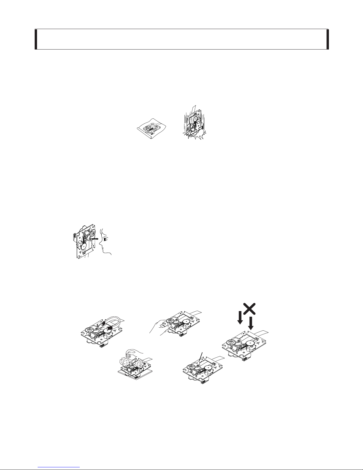
NOTES REGARDING HANDLING OF THE PICK-UP
1. Notes for transport and storage
1) The pick-up should always be left in its conductive bag until immediately prior to use.
2) The pick-up should never be subjected to external pressure or impact.
2. Repair notes
1) The pick-up incorporates a strong magnet, and so should never be brought close to magnetic materials.
2) The pick-up should always be handled correctly and carefully, taking care to avoid external pressure and
impact. If it is subjected to strong pressure or impact, the result may be an operational malfunction and/or
damage to the printed-circuit board.
3) Each and every pick-up is already individually adjusted to a high degree of precision, and for that reason
the adjustment point and installation screws should absolutely never be touched.
4) Laser beams may damage the eyes!
Absolutely never permit laser beams to enter the eyes!
Also NEVER switch ON the power to the laser output part (lens, etc.) of the pick-up if it is damaged.
5) Cleaning the lens surface
If there is dust on the lens surface, the dust should be cleaned away by using an air bush (such as used
for camera lens). The lens is held by a delicate spring. When cleaning the lens surface, therefore, a cotton
swab should be used, taking care not to distort this.
6) Never attempt to disassemble the pick-up.
Spring by excess pressure. If the lens is extremely dirty, apply isopropyl alcohol to the cotton swab. (Do
not use any other liquid cleaners, because they will damage the lens.) Take care not to use too much of
this alcohol on the swab, and do not allow the alcohol to get inside the pick-up.
Storage in conductive bag
Drop impact
NEVER look directly at the laser beam, and don’t let
contact fingers or other exposed skin.
Magnet
How to hold the pick-up
Conductive Sheet
Cotton swab
Pressure
Pressure
- 1-3 -
NOTES REGARDING COMPACT DISC PLAYER REPAIRS
1. Preparations
1) Compact disc players incorporate a great many ICs as well as the pick-up (laser diode). These components
are sensitive to, and easily affected by, static electricity. If such static electricity is high voltage, components
can be damaged, and for that reason components should be handled with care.
2) The pick-up is composed of many optical components and other high-precision components. Care must be
taken, therefore, to avoid repair or storage where the temperature of humidity is high, where strong magnetism is present, or where there is excessive dust.
2. Notes for repair
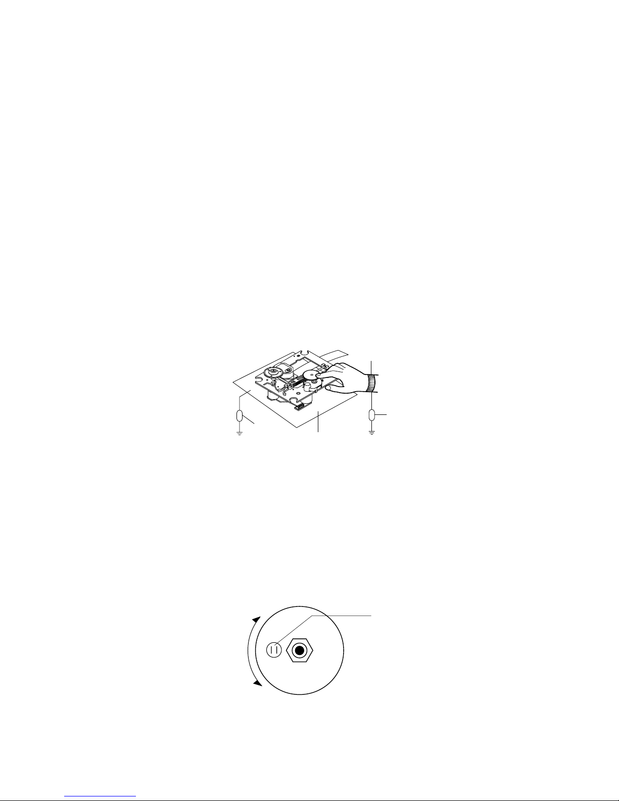
1) Before replacing a component part, first disconnect the power supply lead wire from the unit
2) All equipment, measuring instruments and tools must be grounded.
3) The workbench should be covered with a conductive sheet and grounded.
When removing the laser pick-up from its conductive bag, do not place the pick-up on the bag. (This is
because there is the possibility of damage by static electricity.)
4) To prevent AC leakage, the metal part of the soldering iron should be grounded.
5) Workers should be grounded by an armband (1M Ω)
6) Care should be taken not to permit the laser pick-up to come in contact with clothing, in order to prevent static electricity changes in the clothing to escape from the armband.
7) The laser beam from the pick-up should NEVER be directly facing the eyes or bare skin.
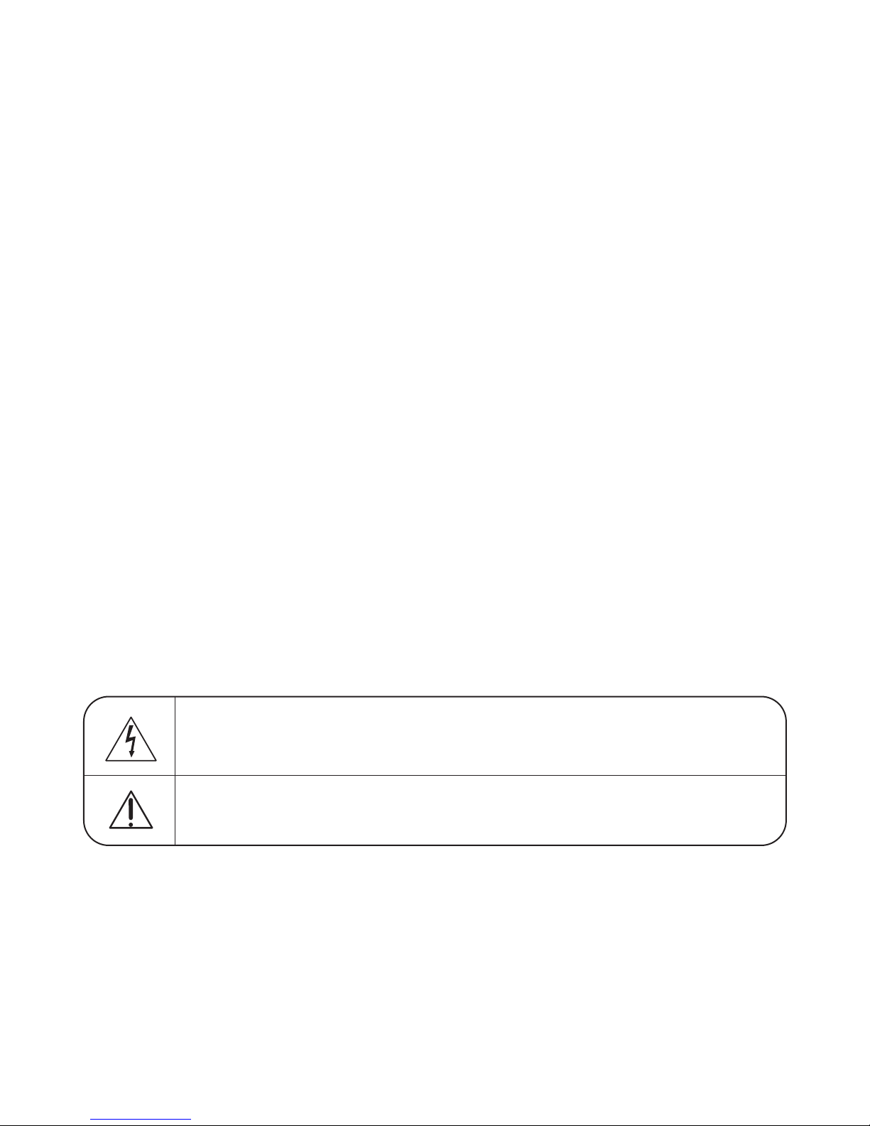
CLEARING MALFUNCTION
You can reset your unit to initial status if malfunction occur(button malfunction, display, etc.).
Using a pointed good conductor(such as driver), simply short the RESET jump wire on the inside of
the volume knob for more than 3 seconds.
If you reset your unit, you must reenter all its settings(stations, clock, timer)
NOTE: 1.To operate the RESET jump wire, pull the volume rotary knob and release it.
2. If you wish to operate the RESET jump wire, it is necessary to unplug the power cord.
Resistor
(1 Mohm)
Conductive
Sheet
Resistor
(1 Mohm)
Armband
RESET jump wire
VOLUME
VOLUME KNOB
DOWN
UP
- 1-4 -
❏ ESD PRECAUTIONS
Electrostatically Sensitive Devices (ESD)
Some semiconductor (solid state) devices can be damaged easily by static electricity. Such components
commonly are called Electrostatically Sensitive Devices (ESD). Examples of typical ESD devices are integrated
circuits and some field-effect transistors and semiconductor chip components.The following techniques should
be used to help reduce the incidence of component damage caused by static electricity.
1. Immediately before handling any semiconductor component or semiconductor-equipped assembly, drain off
any electrostatic charge on your body by touching a known earth ground. Alternatively, obtain and wear a
commercially available discharging wrist strap device, which should be removed for potential shock reasons
prior to applying power to the unit under test.
2. After removing an electrical assembly equipped with ESD devices, place the assembly on a conductive sur-
face such as aluminum foil, to prevent electrostatic charge buildup or exposure of the assembly.
3. Use only a grounded-tip soldering iron to solder or unsolder ESD devices.
4. Use only an anti-static solder removal device. Some solder removal devices not classified as "anti-static" can
generate electrical charges sufficient to damage ESD devices.
5. Do not use freon-propelled chemicals. These can generate electrical charges sufficient to damage ESD
devices.
6. Do not remove a replacement ESD device from its protective package until immediately before you are
ready to install it. (Most replacement ESD devices are packaged with leads electrically shorted together by
conductive foam, aluminum foil or comparable conductive materials).
7. Immediately before removing the protective material from the leads of a replacement ESD device, touch the
protective material to the chassis or circuit assembly into which the device will by installed.
CAUTION : BE SURE NO POWER IS APPLIED TO THE CHASSIS OR CIRCUIT, AND OBSERVE ALL
OTHER SAFETY PRECAUTIONS.
8. Minimize bodily motions when handing unpackaged replacement ESD devices. (Otherwise harmless motion
such as the brushing together of your clothes fabric or the lifting of your foot from a carpeted floor can generate static electricity sufficient to damage an ESD device).
CAUTION. GRAPHIC SYMBOLS
THE LIGHTNING FLASH WITH APROWHEAD SYMBOL. WITHIN AN EQUILATERAL TRIANGLE, IS
INTENDED TO ALERT THE SERVICE PERSONNEL TO THE PRESENCE OF UNINSULATED “DANGEROUS VOLTAGE” THAT MAY BE OF SUFFICIENT MAGNITUDE TO CONSTITUTE A RISK OF
ELECTRIC SHOCK.
THE EXCLAMATION POINT WITHIN AN EQUILATERAL TRIANGLE IS INTENDED TO ALERT THE
SERVICE PERSONNEL TO THE PRESENCE OF IMPORTANT SAFETY INFORMATION IN SERVICE
LITERATURE.
- 2-1 -
SECTION 2. ELECTRICAL
❏ ADJUSTMENTS
This set has been aligned at the factory and normally will not require further adjustment. As a result, it is
not recommended that any attempt is made to modificate any circuit. If any parts are replaced or if anyone tampers with the adjustment, realignment may be necessary.
IMPORTANT
1. Check Power-source voltage.
2. Set the function switch to band being aligned.
3. Turn volume control to minimum unless otherwise noted.
4. Connect low side of signal source and output indicator to chassis ground unless otherwise specified.
5. Keep the signal input as low as possible to avoid AGC and AC action.
TAPE DECK ADJUSTMENT
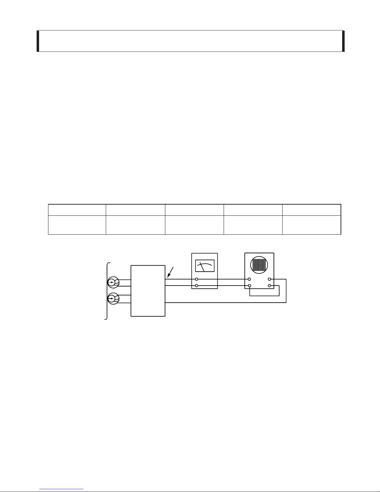
1. AZIMUTH ADJUSTMENT
Figure 1. Azimuth Adjustment Connection Diagram
CH1 CH2
Speaker Out
Playback Mode
Head
Test Tape
MTT-114
L ch
R ch
GND
Dual-trace
synchroscope
Electronic
Voltmeter
L out
R out
Unit
Deck Mode Test Tape Test Point Adjustment Adjust for
Palyback MTT-114 Speaker Out
DECK Screw
Maximum
Azimuth Screw
- 2-2 -
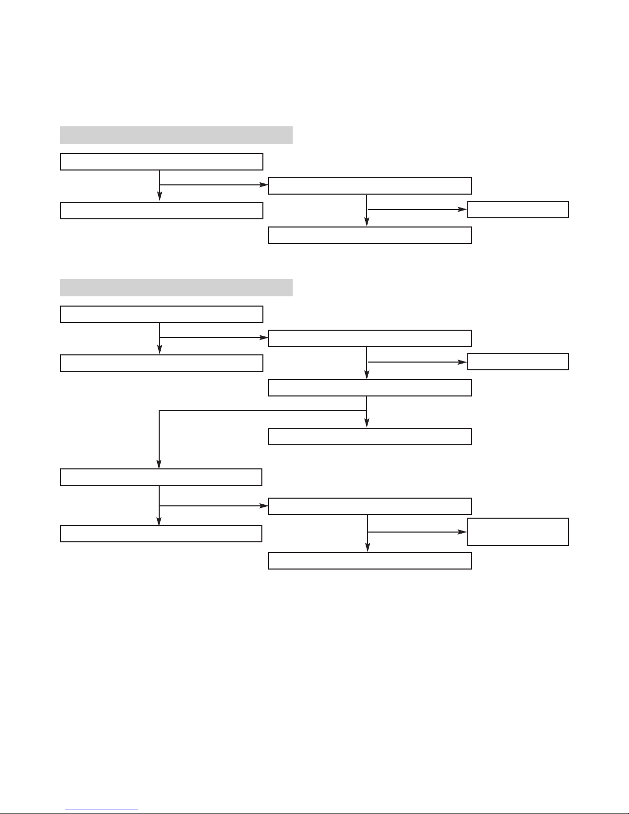
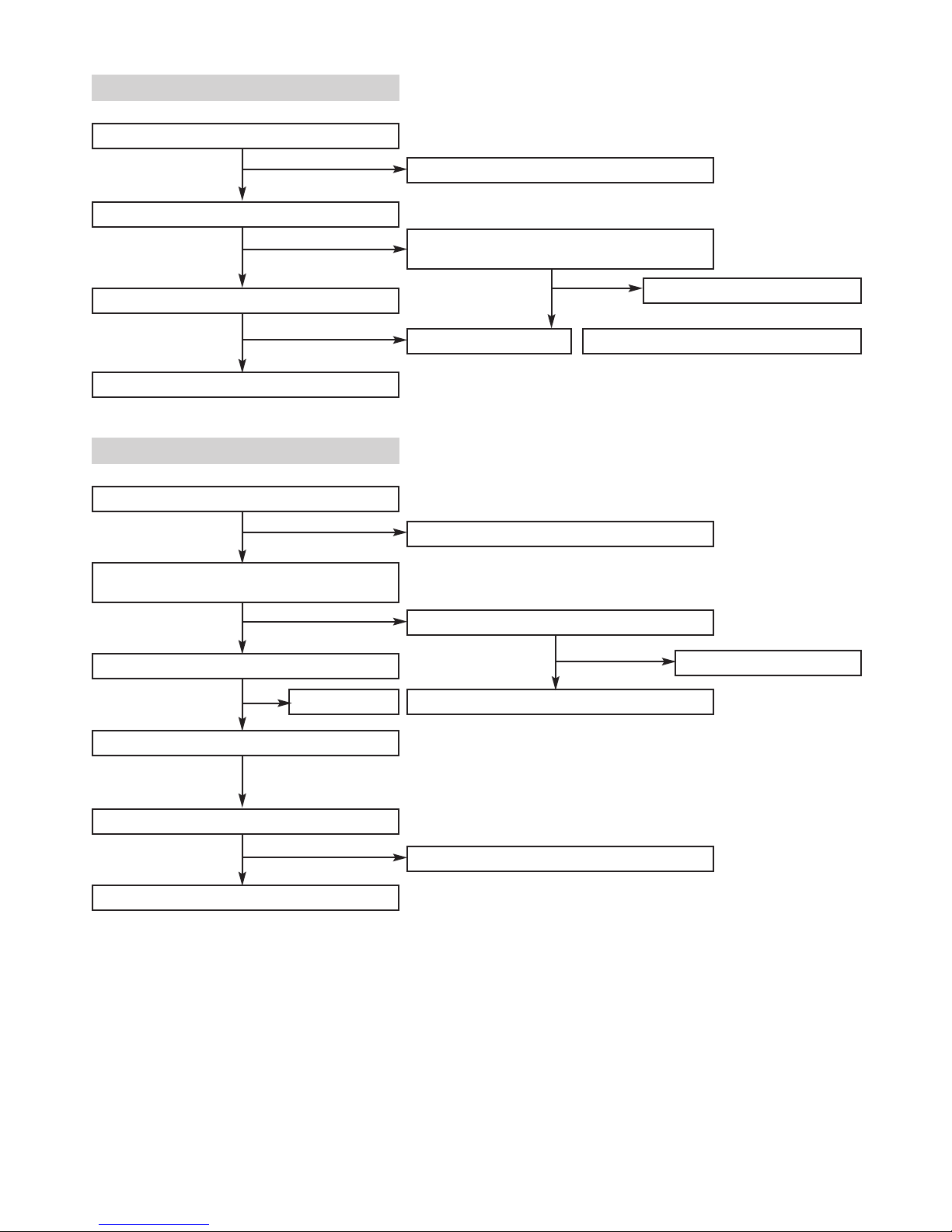
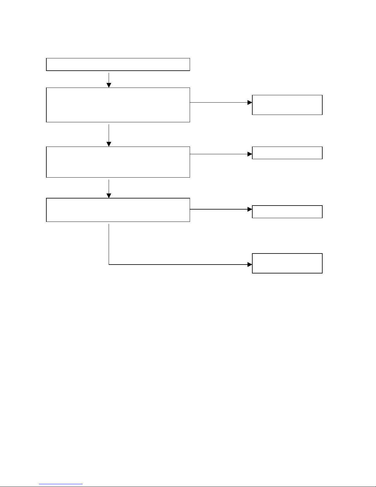
❏ ELECTRICAL TROUBLESHOOTING GUIDE
■ AUDIO PART
P-SENS PART CHECK
ZD 901(5V) Voltage check
IC301 26PIN PATTERN Check
Half-wave rectification wave form check
R783 check, then ZD901 replacement
D713 Replacement
VKK CHECK
CN302 28pin DC -33V check
IC301 51PIN check
ZD902 -33V check
Q903 turn on check
Pattern disconnection check
D912, D911 replacement
normal
ZD902 replacement
Refer to power
supply check
C916 -33V and less check
Q903 replacement
- 2-3 -
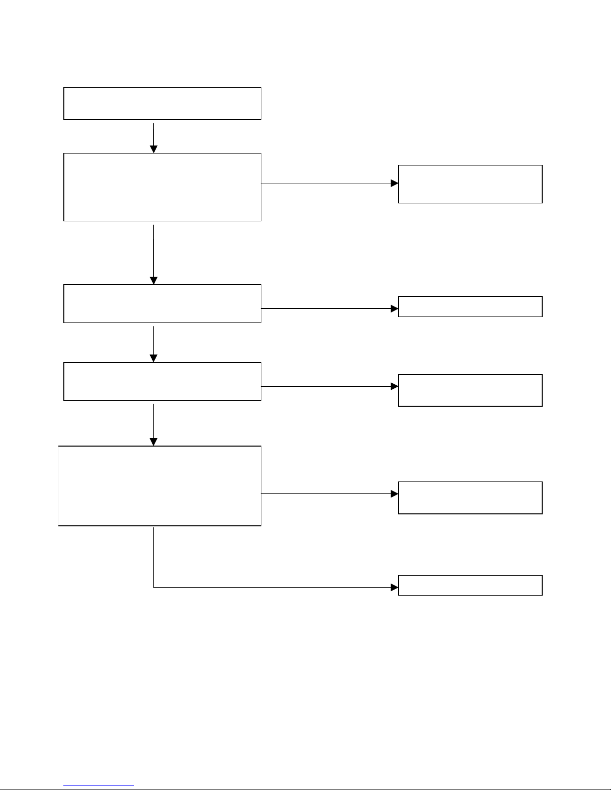
POWER CHECK
Every kinds of Fuse check
C901(+), C902(-) DC power output check
C903(+) DC power output check
IC901, IC902 power output check
IC903 power output check (12V)
CN513 7PIN 5V check (at CD Function)
normal operation
Fuse replace
CN901 1, 5 AC voltage output check
D901 replacement
Power supply Ass’y check
and transformer replacent
IC301 5V Power output
PN302/CN302 13 PIN check
Check
IC5019BU2090 check & replace
IC501(BU2090) 14PIN HIGH check
Q905 Base HIGH(C103M)
Check and replace defective
Power supply Ass’y check
and transformer replacent
CN901, 9, 10 pin DC power output check
IC901, IC902 check and replacement
D902, D903, D904, D905 (1SR35)
check and replacement
IC301 78PIN 5V check
IC904 replacement
Q904(A1273) Base Low check
Q904, CD Ass’y check replacement

- 2-4 -
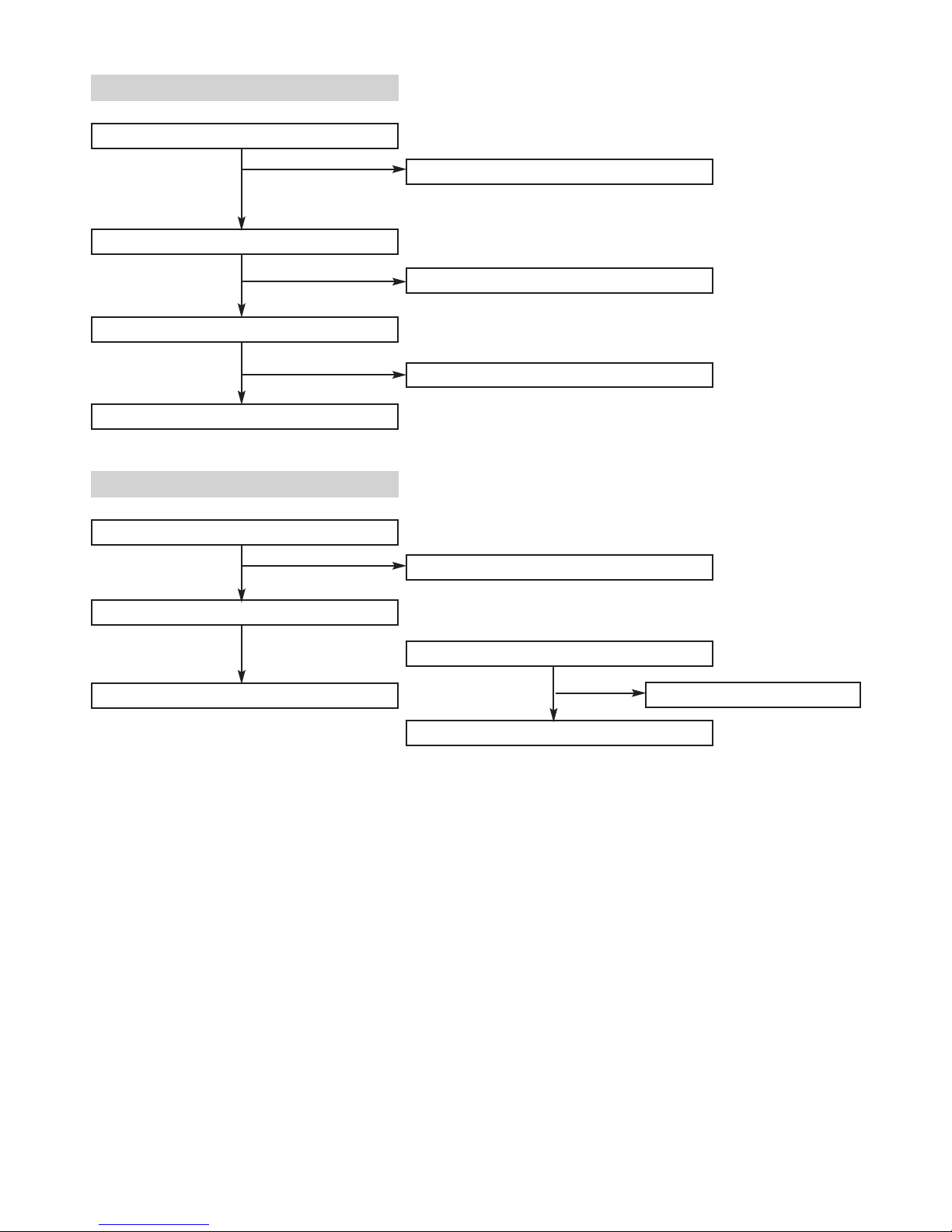
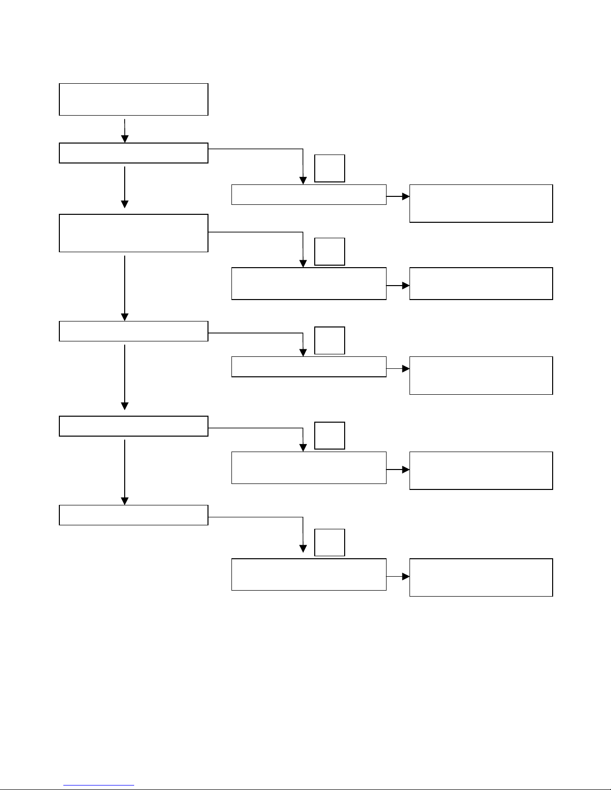
Muting circuit Troubleshooting (if MUTE)
Q702(A102) Base “LOW”
Q701, Q751(IC302) Base “LOW” check
MUTE
Q702 Base and GND operation
status check
Refer to IC601(TDA7468D) IC specification
Refer Muting troubleshooting
Refer SPK replay troubleshooting
IC701 12PIN (over 2V) check and power
supply circuit check
No sound
IC 601 12, 27 PIN Output check
IC701 input check (14PIN)
IC701 output check (6PIN)
RY701 check
normal
- 2-5 -
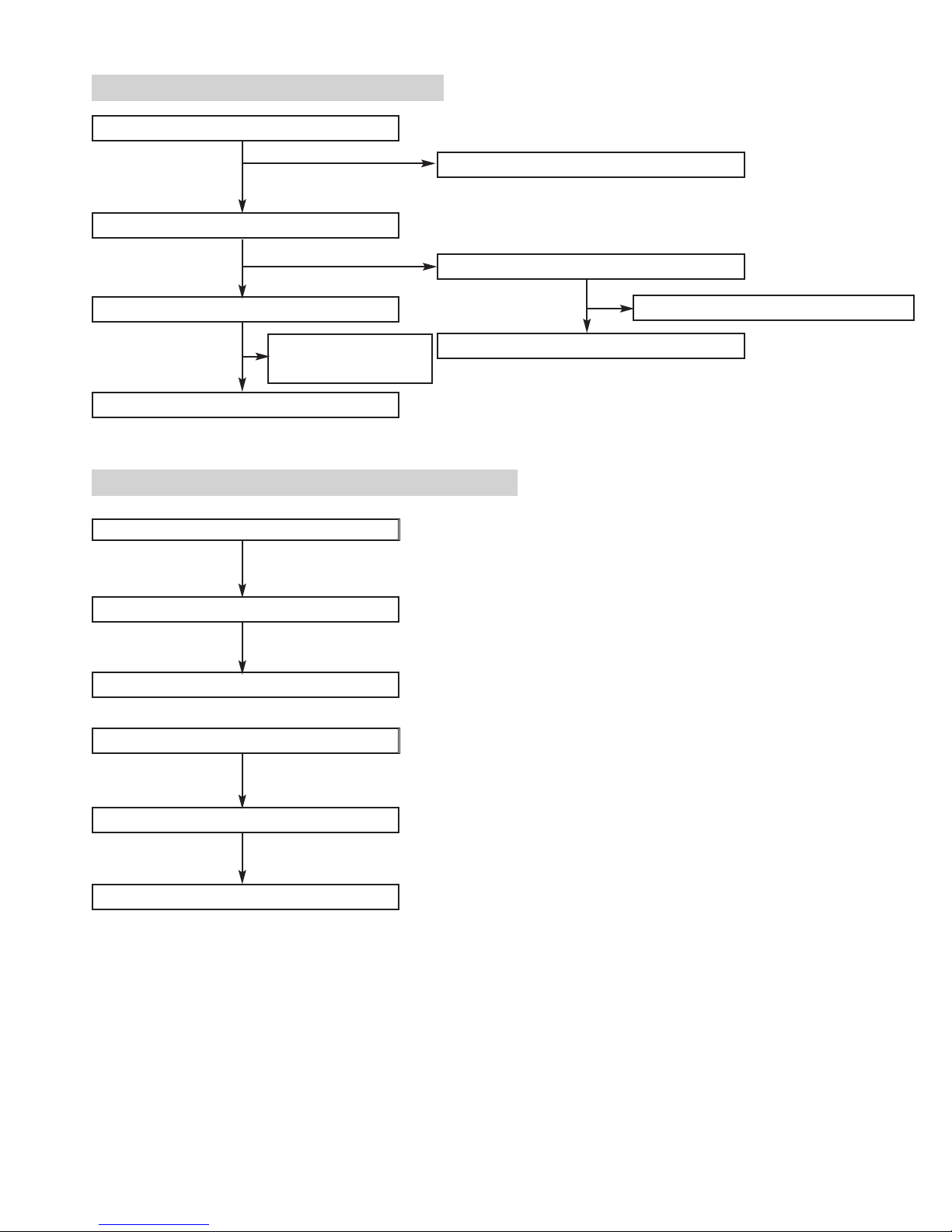
SPK Relay Troubleshooting
D704(+) 12V check
Q704 Collector “Low” check
Output check
normal operation
Refer power check
Q704 Base “High”
Q704 Replacement
RELAY Replacement
(RY701)
Refer IC501(BU2090) Troubleshooting
AUX
IC601 5, 24 PIN signal input check
JK600 signal input check
Specific FUNCTION MODE has no sound
TAPE
IC601 3,26 PIN signal input check
Refer IC202 Troubleshooting
- 2-6 -
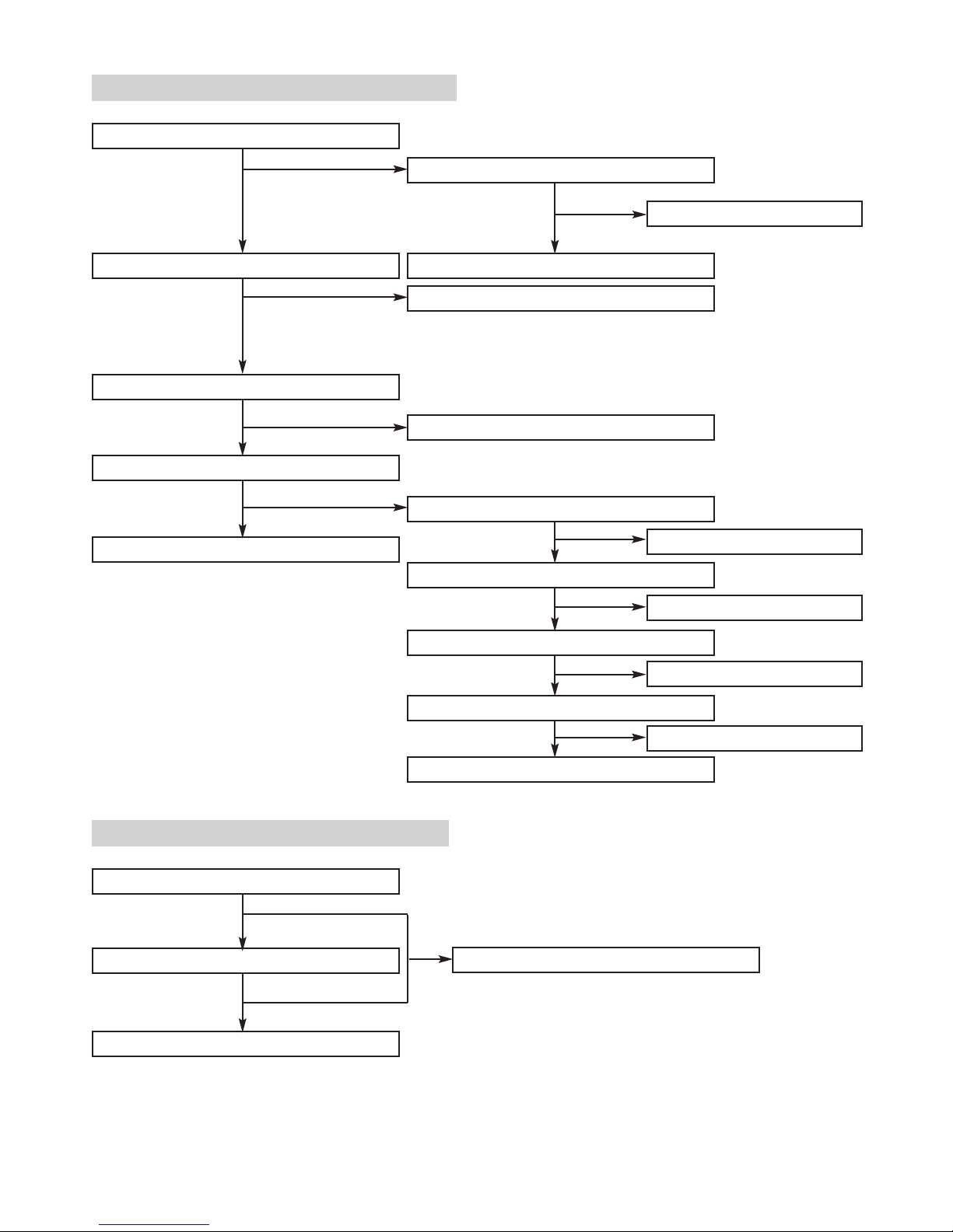
CD
IC601 6,23 PIN signal input check
CN513 1,3 PIN signal check and refer to CD Troubleshooting
TUNER
IC601 4, 25 PIN signal input check
Refer TUNERMODULE
MIC
IC602 2PIN check
Refer to IC404 Troubleshooting
IC301 Troubleshooting
C301 17, 46, 72, 90 power applied check
IC301 26PIN 5V applied check
X301 oscilates or not
When IC301 11Pin voltage input. High➞Low➞High
IC301 replace
Refer to power supply check
P-SENS terminal check
X301 replacement
RESET circuit check
- 2-7 -
IC501 Troubleshooting
IC501 16PIN power applied check
IC501 2, 3 PIN CLK Data check
CONTROL function check
normal
Refer to IC301 Troubleshooting
Refer to power supply check
IC501 replace Pattern check between IC301 and IC501
IC301 3,4 PIN data check
(When switched to CD, TAPE Function)
IC601(TDA7468D) Troubleshooting
IC601 1PIN power applied check
IC601 7,22 Pin waveform output check
IC601 8,21Pin waveform input check
IC601 12,17Pin waveform output check
normal
IC601 15,14 Pulse waveform check
(with tunning VOL DIAL)
Refer to power supply check
IC301 76,75, 5, 10 Pin check
IC601 replacement
MICOM(82,83) - IC401(21,22) Pattern checkIC601 replace
IC301 Troubleshooting
- 2-8 -
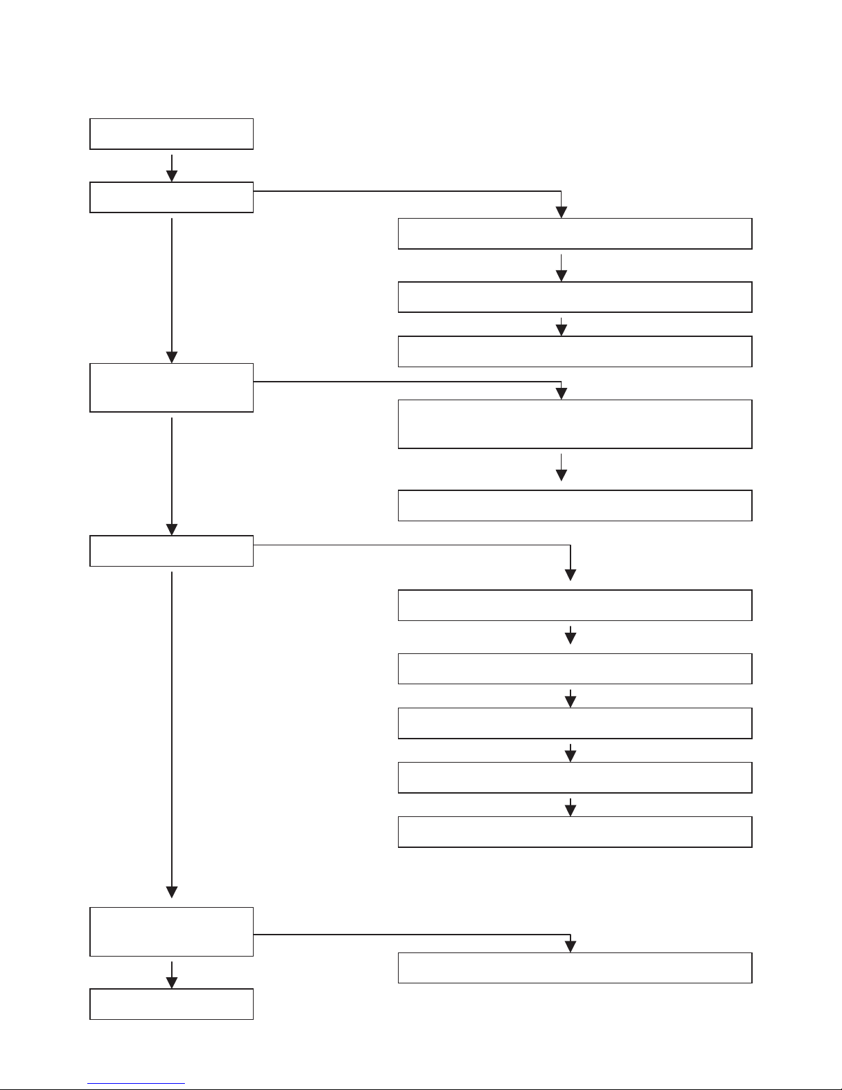
IC701, IC751 Troubleshooting
3PIN signal input check
8, 15Pin(-), 7, 13Pin(+) voltage check
14 Pin signal output check
OK
Refer to Muting circuit
Refer to power supply check
9, 10PIN power check (over 5V)
PLAY check
IC202 18Pin VCC power applied
IC202 5,20 Pin signal output check
Muting circuit check
Refer to power supply check
Deck Mecha operation performance check
Deck Mecha replace
IC202 replacement
- 2-9 -
Rec check (Q252, Q202 ON : R273, R223 High)
IC202 11,14PIN signal input check
IC202 9,16 Pin signal input check
IC201 6(12V), 4 Pin High check
L203 2,3PIN oscilation check
Deck replacement
Q253, Q203 Base "Low" check
Q253,Q203 replacement
Refer to IC203 Troubleshooting
IC202 18Pin VCC voltage check
Power check, IC203 Troubleshooting check
C236(+) power supply check
Refer to power supply check
IC203 Troubleshooting check
Q208 replacement
L203 replacement
Q208 Base 0.6V supplied check
Q208 Collector Low
Q207 replace
normal
Dubbing check ("NORMAL or REC"//"HIGH")
Q252, 202 "OFF"//"ON" : R273,223 "Low"//"HIGH"
Q253,203 "ON"//"OFF"
Refer to REC Check
IC203 Troubleshooting check
- 2-10 -
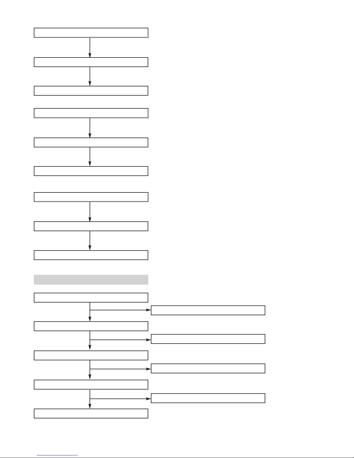
■
CD PART
TURN ON CD
CONNECTOR CHECK ( PN808,PN807 )
CHECK POWER SUPPLY CIRCUIT( PN808 )
CHECK MICOM INTERFACE CIRCUIT( PN807 )
CHECK MICOM INTERFACE CIRCUIT( PN807 )
CONNECTOR CHECK(PN801,PN802)
CHECK PICKUP MOVEMENT
CHECK BA5810FP (IC803)
CHECK MN6627933CG (IC801)
CHECK AN22004 (IC802)
CONNECTOR CHECK (PN808)
CONNECTOR CHECK
( PN808,PN807,PN802,PN801 )
OPEN CLOSE CHECK
“ READING ”
DISPLAY CHECK
READING OK CHECK
IF PLAY, AUDIO
OUTPUT CHECK
OK
YES
YES
YES
YES
YES
NO
NO
NO
NO
- 2-11 -
OPEN CLOSE NG
NO
NO
NO
NO
CONNECTOR LOCKING CHECK ( PN808,PN807 )
DEFECTIVE MAIN
POEWR SUPPLY
DEFECTIVE MICOM
DEFECTIVE IC803
DEFECTIVE
MECHANISM
CHECK POWER SUPPLY CIRCUIT( PN808 ,PN807)
PN808 PIN 5 = 6.2V, PIN 7 = 5V
PN807 PIN 1 = 5V
CHECK VOLTAGE CHANGE OF OPEN CLOSE ,
AND BTLMUTE VOLTAGE(= 5V)
(PN807 PIN 20:OPEN, 19:CLOSE, 4:BTLMUTE)
CHECK VOLTAGE CHANGE LO+, LO- OF IC803
(PN807, PIN OPEN:20, CLOSE:19)
YES
YES
YES
- 2-12 -
READING DISPLAY CHECK (= ONLY “CD “DISPLAY)
CONNECTOR LOCKING CHECK
(PN808,PN807,PN802,PN801 )
DEFECTIVE CONNECTOR OR
MAIN POWER SUPPLAY
DEFECTIVE IC805
DEFECTIVE MICOM OR
CONNECTOR
CHECK RESET SIGNAL OF PN807
PN807 PIN12 : 5V
CHECK VOLTAGE THE PIN 2 OF IC805
IC805 PIN2 : 3.3V
DEFECTIVE MICOM OR
CONNECTOR
DEFECTIVE IC801
CHECK MICOM INTERFACE
CIRCUIT( PN807 )
PN807 PIN 11,13,14,15 SIGNAL CHECK
(11: STAT, 13: MDATA, 14:MCLK, 15:MLD)
CHECK THE WAVE FORM #1
CHECK POWER SUPPLY
PORT( PN808 ,PN807)
PN808 PIN 5 = 6.2V, PIN 7 = 5V
PN807 PIN 1 = 5V
YES
YES
NO
NO
NO
NO
NO
YES
YES
YES
- 2-13 -
AAAA
BBBB
CCCC
DDDD
EEEE
READING OK CHECK (= “NO DISC” DISPLAY)
CONNECTOR LOCKING
CHECK(PN801,PN802)
DOES SLED MOVE ?
DOES LENSE MOVE ?
(= UP & DOWN)
DOES LASER LIGHT ?
DOES SPINDLE ROTATE ?
IS READING OK ?
CHECK PN801 PIN 14,15
(TA- ,TA+)
CHECK PN802 PIN
5,6( SP+,SP-)
CHECK PN802 PIN 10( LD )
CHECK PN801 PIN 13,16
( FA-, FA+)
CHECK PN802 PIN 3,4( SL+,SL-)
DEFECTIVE PICKUP OR
IC803 OR IC801 OR IC802
DEFECTIVE PICKUP OR
IC803 OR IC801
DEFECTIVE PICKUP OR
IC802
DEFECTIVE PICKUP OR
IC803
DEFECTIVE PICKUP OR
IC803 OR IC801 OR IC802
NO
NO
NO
NO
NO
YES
YES
YES
YES
YES
 Loading...