

Page 1
Service Manual
Model : KP275/KP275c
Service Manual
KP275/KP275c
Date: November, 2008 / Issue 1.0
Internal Use Only
Page 2

LGE Internal Use Only
Copyright © 2008 LG Electronics. Inc. All right reserved.
Only for training and service purposes
- 3 -
1. INTRODUCTION ...............................5
1.1 Purpose .................................................. 5
1.2 Regulatory Information............................ 5
1.3 Abbreviations .......................................... 7
2. PERFORMANCE...............................8
2.1 Supporting Standard................................8
2.2 Main Parts: Solution.................................8
2.3 HW Feature..............................................9
2.4 HW Spec................................................11
3. TECHNICAL BRIEF ........................15
3.1 Functional Block Diagram......................15
3.2 Baseband Processor Introduction..........16
3.3 Power management IC ..........................28
3.4 Power ON/OFF ......................................35
3.5 SIM Interface..........................................36
3.6 MICRO SD connector ............................37
3.7 Memory..................................................38
3.8 LCD Display...........................................39
3.9 Keypad switching & scanning ................40
3.10 keypad back-light illumination..............41
3.11 LCD back-light illumination ..................43
3.12 Battery voltage monitor........................44
3.13 Audio....................................................45
3.14 BLUETOOTH.......................................48
3.15 FM Radio .............................................51
3.16 CAMERA connector.............................54
3.17 18PIN Interface connector ...................55
3.18 General Description .............................56
3.19 GSM Part .............................................59
3.20 WCDMA Part .......................................64
3.21 GSM Power Amplifier Module..............66
3.22 WCDMA Band1/5Power Amplifier
Module .................................................67
3.23 WCDMA Band1/5 Low Noise Amplifier68
3.24 WCDMA Band 1/5 Duplexer ................69
4. TROUBLE SHOOTING ...................70
4.1 Trouble shooting test setup....................70
4.2 Power on trouble....................................71
4.3 Charging Trouble ...................................74
4.4 UBS Trouble ..........................................77
4.5 SIM Detect Trouble................................79
4.6 Number Key Sense Trouble...................82
4.7 Multi Key sense Trouble ........................84
4.8 Keypad backlight Trouble ......................86
4.9 Micro SD Trouble...................................88
4.10 Audio Trouble.......................................90
4.11 Microphone Trouble.............................94
4.12 Camera Trouble...................................98
4.13 Main LCD Trouble..............................103
4.14 Bluetooth Trouble...............................105
4.15 FM Radio ...........................................108
4.16 RF Component...................................112
4.17 RF SIGNAL PATH .............................113
4.18 Trouble Shooting of GSM Part ..........114
4.19 Trouble Shooting of WCDMA Part.....122
5. DOWNLOAD.....................................128
5.1 USB Driver Installation to Download....128
5.2 Device Detection..................................130
5.3 USB Port Mapping ...............................131
5.4 Configuration to Download...................132
5.5 Nexus setting .......................................134
6. CIRCUIT DIAGRAM ......................135
7. BGM PIN MAP...............................143
8. PCB LAYOUT................................149
9. RF Calibration ..............................155
9.1 Test Equipment Setup .........................155
9.2 Calibration Step ...................................155
10. EXPLODED VIEW &
REPLACEMENT PART LIST ......161
10.1 Exploded View ...................................161
10.2 Replacement Parts ............................163
10.3 Accessory ..........................................184
Table Of Contents
Page 3

- 4 -
LGE Internal Use Only
Copyright © 2008 LG Electronics. Inc. All right reserved.
Only for training and service purposes
Page 4

- 5 -
1. INTRODUCTION
1.1 Purpose
This manual provides the information necessary to repair, calibration, description and download the
features of the KP275C.
1.2 Regulatory Information
A. Security
Toll fraud, the unauthorized use of telecommunications system by an unauthorized part (for example,
persons other than your company’s employees, agents, subcontractors, or person working on your
company’s behalf) can result in substantial additional charges for your telecommunications services.
System users are responsible for the security of own system.
There are may be risks of toll fraud associated with your telecommunications system. System users
are responsible for programming and configuring the equipment to prevent unauthorized use. LGE
does not warrant that this product is immune from the above case but will prevent unauthorized use of
common carrier telecommunication service of facilities accessed through or connected to it. LGE will
not be responsible for any charges that result from such unauthorized use.
B. Incidence of Harm
If a telephone company determines that the equipment provided to customer is faulty and possibly
causing harm or interruption in service to the telephone network, it should disconnect telephone
service until repair can be done. A telephone company may temporarily disconnect service as long as
repair is not done.
C. Changes in Service
A local telephone company may make changes in its communications facilities or procedure. If these
changes could reasonably be expected to affect the use of the KP275C or compatibility with the net
work, the telephone company is required to give advanced written notice to the user, allowing the user
to take appropriate steps to maintain telephone service.
D. Maintenance Limitations
Maintenance limitations on the KP275C must be performed only by the LGE or its authorized agent.
The user may not make any changes and/or repairs expect as specifically noted in this manual.
Therefore,note that unauthorized alternations or repair may affect the regulatory status of the system
and may void any remaining warranty.
1. INTRODUCTION
LGE Internal Use Only
Copyright © 2008 LG Electronics. Inc. All right reserved.
Only for training and service purposes
Page 5

- 6 -
1. INTRODUCTION
E. Notice of Radiated Emissions
This model complies with rules regarding radiation and radio frequency emission as defined by local
regulatory agencies. In accordance with these agencies, you may be required to provide information
such as the following to the end user.
F. Pictures
The pictures in this manual are for illustrative purposes only; your actual hardware may look slightly
different.
G. Interference and Attenuation
An KP275C may interfere with sensitive laboratory equipment, medical equipment, etc. Interference
from unsuppressed engines or electric motors may cause problems.
H. Electrostatic Sensitive Devices
ATTENTION
Boards, which contain Electrostatic Sensitive Device (ESD), are indicated by the Following
information is ESD handling:
• Service personnel should ground themselves by using a wrist strap when exchange system boards.
• When repairs are made to a system board, they should spread the floor with anti-static mat which is
also grounded.
• Use a suitable, grounded soldering iron.
• Keep sensitive parts in these protective packages until these are used.
• When returning system boards or parts like EEPROM to the factory, use the protective package as
described.
LGE Internal Use Only
Copyright © 2008 LG Electronics. Inc. All right reserved.
Only for training and service purposes
Page 6
- 7 -
1. INTRODUCTION
1.3 Abbreviations
For the purposes of this manual, following abbreviations apply:
LGE Internal Use Only
Copyright © 2008 LG Electronics. Inc. All right reserved.
Only for training and service purposes
APC Automatic Power Control
BB Baseband
BER Bit Error Ratio
CC-CV Constant Current - Constant Voltage
DAC Digital to Analog Converter
DCS Digital Communication System
dBm dB relative to 1 milliwatt
DSP Digital Signal Processing
EEPROM Electrical Erasable Programmable Read-Only Memory
EL Electroluminescence
ESD Electrostatic Discharge
FPCB Flexible Printed Circuit Board
GMSK Gaussian Minimum Shift Keying
GPIB General Purpose Interface Bus
GSM Global System for Mobile Communications
IPUI International Portable User Identity
IF Intermediate Frequency
LCD Liquid Crystal Display
LDO Low Drop Output
LED Light Emitting Diode
OPLL Offset Phase Locked Loop
PAM Power Amplifier Module
PCB Printed Circuit Board
PGA Programmable Gain Amplifier
PLL Phase Locked Loop
PSTN Public Switched Telephone Network
RF Radio Frequency
RLR Receiving Loudness Rating
RMS Root Mean Square
RTC Real Time Clock
FEM Front End Module
SIM Subscriber Identity Module
SLR Sending Loudness Rating
SRAM Static Random Access Memory
STMR Side Tone Masking Rating
TA Travel Adapter
TDD Time Division Duplex
TDMA Time Division Multiple Access
UART Universal Asynchronous Receiver/Transmitter
VCO Voltage Controlled Oscillator
VCTCXO Voltage Control Temperature Compensated Crystal Oscillator
WAP Wireless Application Protocol
Page 7
LGE Internal Use Only
Copyright © 2008 LG Electronics. Inc. All right reserved.
Only for training and service purposes
2. PERFORMANCE
2. PERFORMANCE
- 8 -
2.1 Supporting Standard
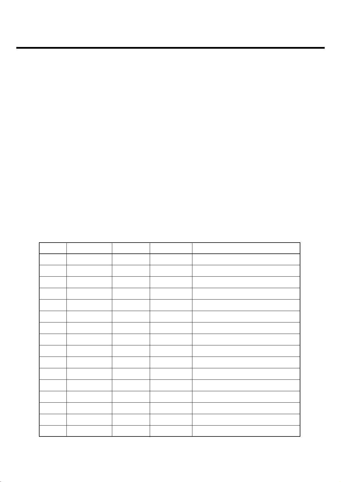
2.2 Main Parts: Solution
Item Feature Comment
Supporting Standard WCDMA850 / WCDMA 2100
EGSM900 / DCS1800 / PCS1900
seamless handover
Phase 2+(include AMR)
SIM Toolkit : Class 1, 2, 3, A-E
Frequency Range EGSM900 TX : 880 - 915MHz
EGSM900 RX : 925 - 960 MHz
DCS1800 TX : 1710 - 1785 MHz
DCS1800 RX : 1805 - 1880 MHz
PCS1900 TX : 1850 - 1910 MHz
PCS1900 RX : 1930 - 1990 MHz
WCDMA850 TX : 824 - 849MHz
WCDMA850 RX : 869 - 894MHz
WCDMA2100 TX : 1920 - 1980 MHz
WCDMA2100 RX : 2110 - 2170 MHz
Application Standard WAP 2.0, JAVA 2.0
Item Part name Comment
Digital Baseband PMB8868 (Infineon)
Analog Baseband PMB8868 (Infineon)
RF chip PMB6952 (Infineon)
Page 8
- 9 -
2. PERFORMANCE
LGE Internal Use Only
Copyright © 2008 LG Electronics. Inc. All right reserved.
Only for training and service purposes
2.3 HW Feature
Item Feature Comment
Form Factor Slide type
Battery 1)Capacity
Standard : Li-Ion, 900mAh
2) Packaging Type : Soft Pack
Size 98 x 48 x 16.9 mm
Weight 98 g With Battery
GSM 280 hours @paging period 5
WCDMA 200hours @DRX=128frames
GSM 160min @ Power Level 7
WCDMA 160min @Tx=12dBm
Charging time 3 hours @power OFF/900mAh
RX sensitivity GSM850 : -105 dBm
DCS1800 : -105 dBm
PCS1900 : -105 dBm
WCDMA 850 : -106.7dBm
WCDMA2100 : -106.7 dBm
GSM850 : 33 dBm Class4 (EGSM900)
DCS1800 : 30 dBm Class1(DCS)
PCS1900 : 30 dBm Class1(PCS)
EGSM900 : 27 dBm E2 (EGSM900)
DCS1800 : 26 dBm E2 (DCS)
PCS1900 : 26 dBm E2 (PCS)
GPRS compatibility GPRS Class 12
EDGE compatibility EDGE Class 12
Display Main LCD(2”, 176 x 220)/TFT
Built-in Camera 1.3 Mega pixel, VT CAM(VGA)
ANT Main : Internal Fixed Type
System connector 18 Pin
Ear Phone Jack 18pin, 4 Pole, Stereo
PC synchronization Yes
TX output
power
GSM/
GPRS
EDGE
Stand-by
time
Talk time
Page 9
- 10 -
2. PERFORMANCE
LGE Internal Use Only
Copyright © 2008 LG Electronics. Inc. All right reserved.
Only for training and service purposes
Item Feature Comment
Speech coding FR, EFR, HR, AMR
Vibrator Built in Vibrator
Blue Tooth V1.2, A2DP
Voice Recording Yes
Speaker Phone mode Yes
Support
Travel Adapter Yes
CDROM Yes
Stereo Headset Yes
Data Cable No
T-Flash Yes Not Equipped
Page 10
- 11 -
2. PERFORMANCE
LGE Internal Use Only
Copyright © 2008 LG Electronics. Inc. All right reserved.
Only for training and service purposes
2.4 HW Spec.
2.4.1 GSM Transmitter/Receiver spec.
Item Specification
1Frequency Band EGSM900
TX : 880 - 915MHz
RX : 925 - 960 MHz
DCS1800
TX : 1710 - 1785 MHz
RX : 1805 - 1880 MHz
PCS1900
TX : 1850 - 1910 MHz
RX : 1930 - 1990 MHz
2 Phase Error Rms : 5°
Peak : 20°
3 Frequency Error GSM : 0.1 ppm
DCS/PCS : 0.1 ppm
4 EMC(Radiated Spurious GSM/DCS : < -28dBm
Emission Disturbance)
5 Transmitter Output power and GSM : 5dBm - 33dBm 3dB
Burst Timing DCS/PCS : 0dBm - 30dBm 3dB
6 Burst Timing < 3.69us
7 Spectrum due to modulation out 200kHz : -36dBm
to less than 1800kHz offset 600kHz : -51dBm/-56dBm
8 Spectrum due to modulation out GSM
to larger than 1800kHz offset to 1800-3000kHz :< -63dBc(-46dBm)
the edge of the transmit band 3000kHz-6000kHz : <-65dBc(-46dBm)
6000kHz < : < -71dBc(-46dBm)
DCS
1800-3000kHz :< -65dBc(-51dBm)
6000kHz < : < -73dBc(-51dBm)
Page 11
- 12 -
2. PERFORMANCE
LGE Internal Use Only
Copyright © 2008 LG Electronics. Inc. All right reserved.
Only for training and service purposes
Item Specification
9 Spectrum due to switching 400kHz : -19dBm/-22dBm(5/0), -23dBm
transient 600kHz : -21dBm/-24dBm(5/0), -26dBm
10 Reference Sensitivity - TCH/FS Class II(RBER) : -105dBm(2.439%)
11 Usable receiver input level range 0.012(-15 - -40dBm)
12 Intermodulation rejection - 800kHz, 1600kHz : -98dBm / -96dBm (2.439%)
Speech channels
13 AM Suppression -98dBm/-96dBm (2.439%)
- GSM : -31dBm
- DCS : -29dBm
14 Timing Advance 0.5T
Page 12
- 13 -
2. PERFORMANCE
LGE Internal Use Only
Copyright © 2008 LG Electronics. Inc. All right reserved.
Only for training and service purposes
2.4.2 WCDMA Transmitter spec.
Item Specification
1 Transmit Frequency WCDMA 850 : 824 MHz ~ 849 MHz
WCDMA 2100 : 1920 MHz ~ 1980 MHz
2 Maximum Output Power +24 dBm / 3.84 MHz, +1 / -3 dB
3 Frequency Error within 0.1 PPM
4 Open Loop Power Control Normal Conditions : within 9 dB,
Extreme Conditions : within 12 dB
5 Minimum Transmit Power < -50 dBm / 3.84 MHz
6 Occupied Bandwidth < 5 MHz at 3.84 Mcps (99% of power)
7 Adjacent Channel Leakage > 33 dB @ 5 MHz,
Power Ratio (ACLR) > 43 dB @ 10 MHz
8 Spurious Emissions < -36 dBm / 1 kHz RW @ 9 kHz ≤ f < 150 kHz
|f-fc| > 12.5 MHz < -36 dBm / 10 kHz RW @ 150 KHz ≤ f < 30 MHz
< -36 dBm / 100 kHz RW @ 30 MHz ≤ f < 1 GHz
< -30 dBm / 1 MHz RW @ 1 GHz ≤ f < 12.75 GHz
< -41 dBm / 300 kHz RW @ 1893.5 MHz < f < 1919.6 MHz
< -67 dBm / 100 kHz RW @ 925 MHz ≤ f ≤ 935 MHz
< -79 dBm / 100 kHz RW @ 935 MHz < f ≤ 960 GHz
< -71 dBm / 100 kHz RW @ 1805 MHz ≤ f ≤ 1880 MHz
9 Transmit Intermodulation < -31 dBc @ 5 MHz & < -41 dBc @ 10 MHz
when Interference CW Signal Level = -40 dBc
10 Error Vector Magnitude < 17.5 %, when Pout ≥ -20 dBm
11 Peak Code Domain Error < -15 dB at Pout ≥ -20 dBm
Page 13
LGE Internal Use Only
Copyright © 2008 LG Electronics. Inc. All right reserved.
Only for training and service purposes
2. PERFORMANCE
- 14 -
2.4.3 WCDMA Receiver spec.
Item Specification
1 Receive Frequency WCDMA 850 : 869 MHz ~ 894 MHz
WCDMA 2100 : 2110MHz ~ 2170 MHz
2 Reference Sensitivity Level WCDMA 850 :
BER < 0.001 when Îor = -104.7 dBm / 3.84 MHz
WCDMA 2100 :
BER < 0.001 when Îor = -106.7 dBm / 3.84 MHz
3 Maximum Input Level BER < 0.001 when Îor = -25 dBm / 3.84 MHz
4 Adjacent Channel Selectivity ACS > 33 dB where BER < 0.001 when Îor =
(ACS) -92.7 dBm / 3.84 MHz
& Ioac = -52 dBm / 3.84 MHz @ 5 MHz
5Blocking Characteristic BER < 0.001 when Îor = -103.7 dBm / 3.84 MHz
& Iblocking = -56 dBm / 3.84 MHz @ Fuw(offset)
= 10 MHz
or Iblocking = -44 dBm / 3.84 MHz @ Fuw(offset)
= 15 MHz
6 Spurious Response BER < 0.001 when Îor = -103.7 dBm / 3.84 MHz &
Iblocking = -44 dBm
7 Intermodulation BER < 0.001 when Îor= -103.7 dBm / 3.84 MHz
& Iouw1 = -46 dBm @ Fuw1(offset) = 10 MHz
& Iouw2 = -46 dBm / 3.84 MHz @ Fuw2(offset) =
20 MHz
8 Spurious Emissions < -57 dBm / 100 kHz BW @ 9 kHz ≤ f < 1 GHz
< -47 dBm / 1 MHz BW @ 1 GHz ≤ f ≤ 12.75 GHz
9 nner Loop Power control in uplink Adjust output(TPC command)
cmd 1dB 2dB 3dB
+1 +0.5/1.5 +1/3 +1.5/4
0 -0.5/+0.5 -0.5/+0.5 -0.5/+0.5
-1 -0.5/-1.5 -1/-3 -1.5/-4
group(10equal command group)
+1 +8/+12 +16/+24
Page 14
LGE Internal Use Only
Copyright © 2008 LG Electronics. Inc. All right reserved.
Only for training and service purposes
3. TECHNICAL BRIEF
- 15 -
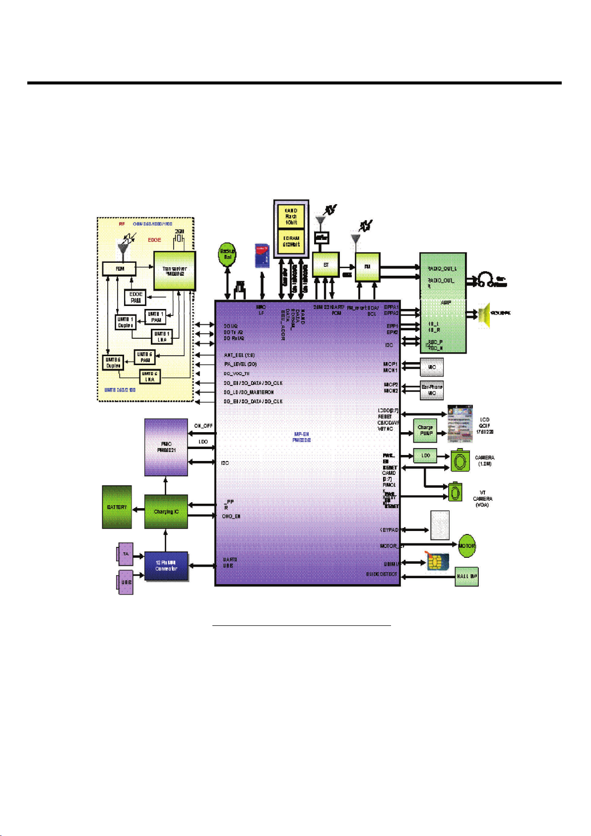
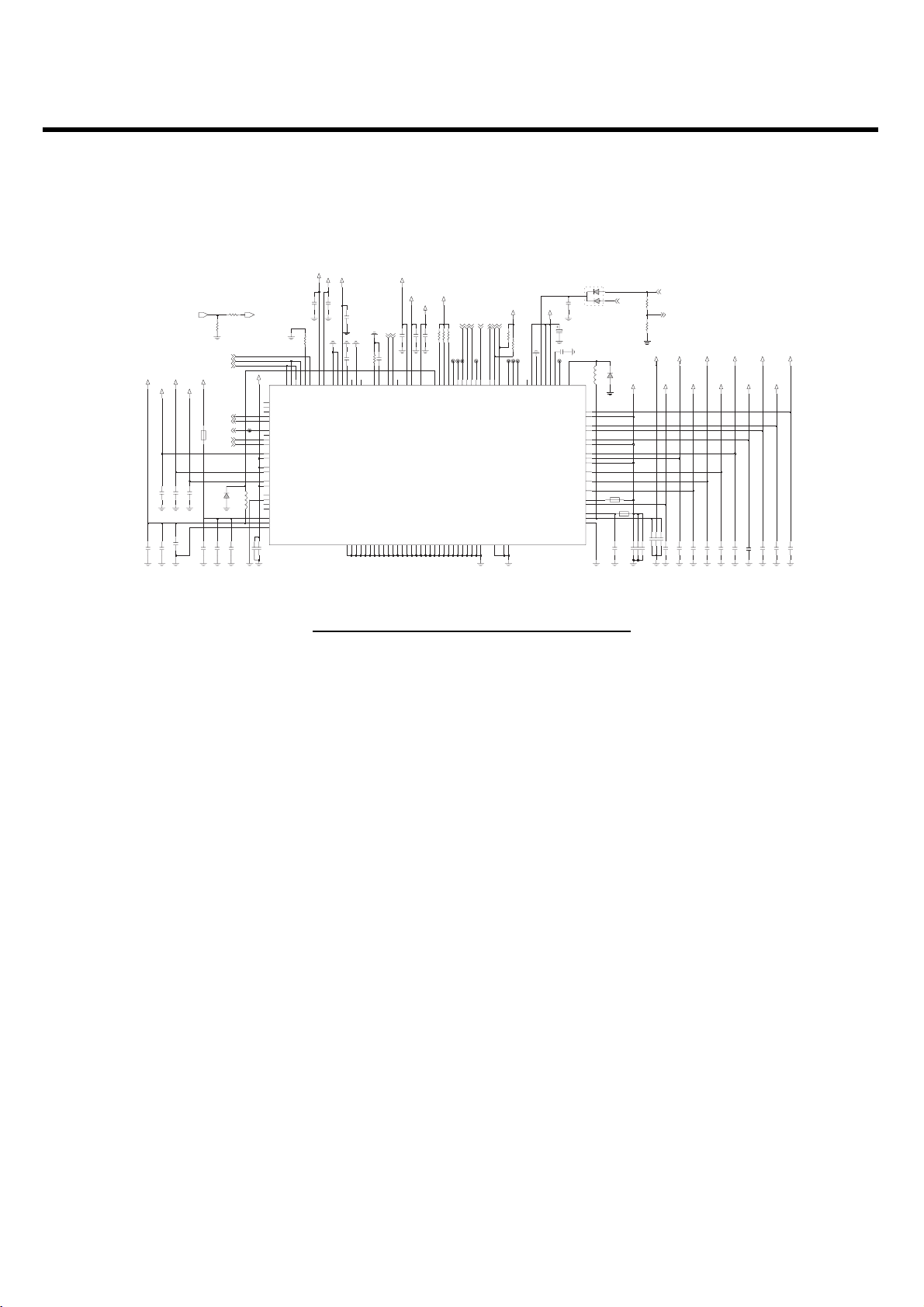
3.1 Functional Block Diagram
3. TECHNICAL BRIEF
[Figure 3.1] Functional Block Diagram
Page 15
- 16 -
3. TECHNICAL BRIEF
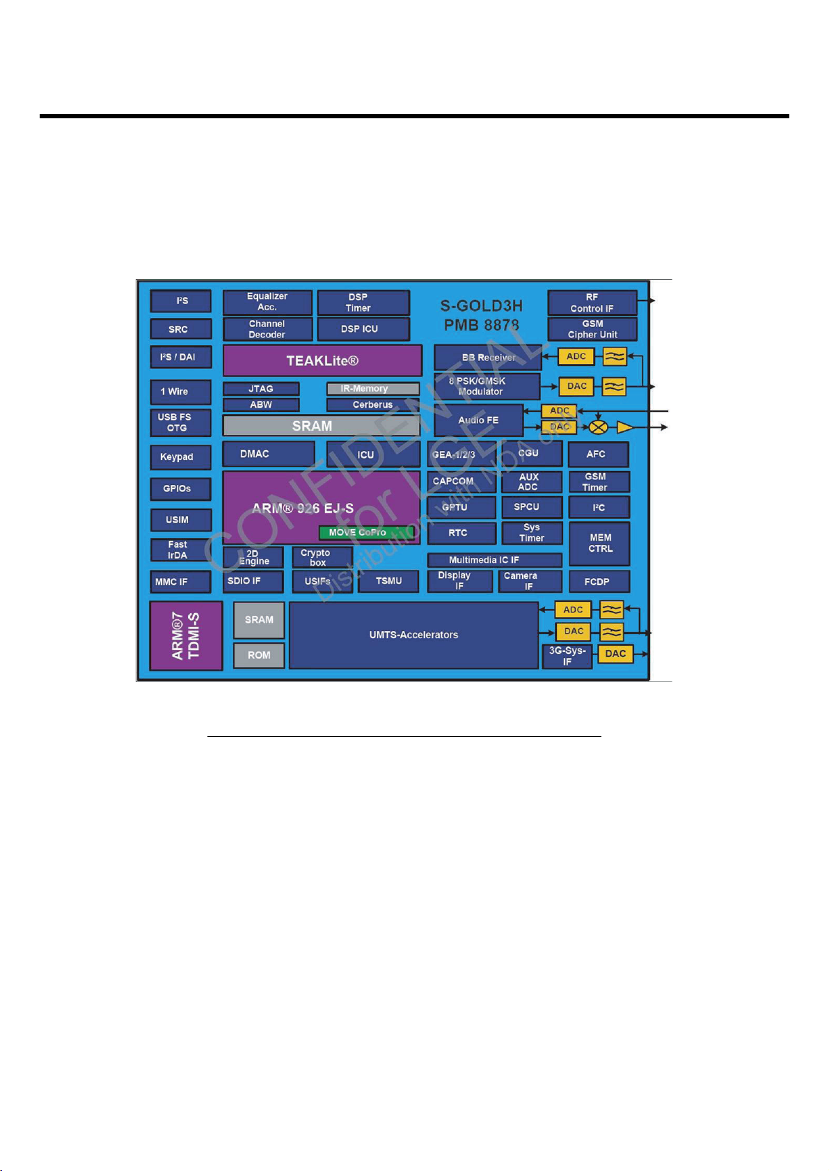
3.2 Baseband Processor Introduction
3.2.1 General description
S-GOLD3H-LC is a HSDPA/WCDMA/EDGE/GPRS/GSM system in package solution consisting of a
mixed signal baseband IC with a 3G coprocessor IC.
l Baseband IC containing all analog and digital functionality of a cellular radio. Additionally SGOLD3TM
Provides multimedia extensions such as camera, software MIDI, MP3 sound. It is designed as a single
chip solution, integrating the digital and mixed signal portions of the base band in 0.09um, 1.2V
technology.
The chip will support the FR, EFR, HR and AMR-NB vocoding.
S-GOLD3™ support multi-slot operation modes HSCSD (up to class 10), GPRS for high speed data
application (up to class 12), EGPRS (up to class 12) and DTM(class11) without additional external
hardware.
LGE Internal Use Only
Copyright © 2008 LG Electronics. Inc. All right reserved.
Only for training and service purposes
[Figure 3.2] Top level block diagram of the MPEH(PMB8868)
Page 16

- 17 -
3. TECHNICAL BRIEF
3.2.2 Block Description
• Processing core
ARM926EJ-S 32 bit processor core for controller functions. The ARM926EJ-S includes an MMU,
and the Jazelle Java extension for Java acceleration.
- TEAKLite DSP core
• ARM-Memory
- 32k Byte Boot ROM on the AHB
- 128k Byte SRAM on the AHB, flexibly usable as program or data RAM
- 32k Byte Instruction Cache
- 32k Byte Data Cache
- 8k Byte Instruction Tightly coupled Memory(I-TCM)
- 8k Byte Data tightly coupled memory (D-TCM)
• DSP-Memory
- 120k x 16bit Program ROM
- 8k x 16bit Program RAM
- 72k x 16bit Data ROM
- 48k x 16bit Data XRAM
- 5k x 16bit Data YRAM
- Incremental Redundancy(IR) Memory of 35904 words of 16bit
• Shared Memory Block
1.5K x 32bit Shared RAM(dual ported) between controller system and TEAKLite.
• Controller Bus system
The processor cores and their peripherals are connected by powerful buses.
-Multi-layer AHB for connecting the ARM and the other master capable building blocks with
theinternal and external memories and with the peripheral buses.
-An FPI-Bus for connecting GSM peripherals, called hereafter FPI3 bus.
-A controller FPI bus for connecting the low performance controller peripherals such as keypad,
Called hereafter fPI2 bus.
-FPI2 and FPI3 are connected asynchronously to the AHB buses.
• Clock system
The clock system allows widely independent selection of frequencies for the essential parts of the
SGOLD3H-LC. Thus power consumption and performance can be optimized for each application.
LGE Internal Use Only
Copyright © 2008 LG Electronics. Inc. All right reserved.
Only for training and service purposes
Page 17
- 18 -
3. TECHNICAL BRIEF
• Functional Hardware block
- CPU and DSP Timers
- MOVE coprocessor performing motion estimation for video encoding algorithms(H.263, MPEG-4)
- Programmable PLL with additional phase shifters for system clock generation
- GSM Timer Module that off-loads the CPU from radio channel timing
- GMSK / 8-PSK Modulator according to GSM-standard 05.04 (5/2000)
- GMSK Modulator: gauss-filter with B*T=0.3
- EDGE Modulator: 8PSK-modulation with linearized GMSK-Pulse-Filter
- Hardware accelerators for equalizer and channel decoding.
- Incremental Redundancy memory for EDGE class 12 support
- A5/1, A5/2, A5/3 Cipher unit
- GEA1, GEA2, GEA3 Cipher Unit to support GPRS data transmission
- Advanced static and dynamic power management features including TDMA-Frame synchronous
low power mode and enhanced CPU modes(idle and sleep modes)
3.2.3 RF Interface(T_OUT)
S-Gold3H-LC uses this interface to control RF IC and Peripherals.
[Table 3.2.3-1] RF Interface Spec.
LGE Internal Use Only
Copyright © 2008 LG Electronics. Inc. All right reserved.
Only for training and service purposes
T_OUT
Resource Interconnection Description
T_OUT0 TXON_PA PAM Power on
T_OUT1 T_OUT2 ANT_SEL1
T_OUT3
T_OUT4 FEM control
T_OUT5 FEM control
T_OUT6 PA_MODE PAM Mode select
T_OUT7 ANT_SEL2
T_OUT8 ANT_SEL3
T_OUT9
T_OUT10
Page 18
- 19 -
3. TECHNICAL BRIEF
3.2.4 ADC channel
ADC block is composed of 11 external ADC channel. This block operates charging process and other
related process by reading battery voltage and other analog values.
[Table 3.2.4-1] S-Gold3 ADC channel usage
LGE Internal Use Only
Copyright © 2008 LG Electronics. Inc. All right reserved.
Only for training and service purposes
ADC channel
Resource Interconnection Description
M0 BAT_ID Battery temperature measure
M1 RF_TEMP RF block temperature measure
kM2 N.C
M3 JACK_TYPE Accessory type detect
M4 N.C
M5 N.C
M6 N.C
M7 H/W VERSION H/W version detect
M8 VBAT Battery supply voltage measure
M9 N.C
M10 N.C
Page 19
3.2.5 GPIO map
Over a hundred allowable resources, KP275C is using as follows except dedicated to SIM and
Memory.
KP275C GPIO(General Purpose Input/Output) Map, describing application, I/O state, and enable level,
is shown in below table
[Table 3.2.5-1] S-Gold3H-LC GPIO pin Map
- 20 -
3. TECHNICAL BRIEF
LGE Internal Use Only
Copyright © 2008 LG Electronics. Inc. All right reserved.
Only for training and service purposes
Port Function Net Name Description
KEY MATRIX
KP_IN0 KEYIN0
KP_IN1 KEYIN1
KP_IN2 KEYIN2
KP_IN3 KEYIN3
KP_IN4 KEYIN4
KP_IN5 KEYIN05
KP_IN6 KEYOUT5
KP_OUT0 KEYOUT0
KP_OUT1 KEYOUT1
KP_OUT2 KEYOUT2
KP_OUT3 KEYOUT3
USIF1
USIF1_RXD_MRST UART_RX UART Data
USIF1_TXD_MTSR UART_TX UART Data
USIF1_RTS_N USB_ DAT_VP USB Data
USIF1_CTS_N USB_SE0_VM USB Data
USIF2
USIF2 _RXD_MRST BT_UART_RX Bluetooth UART Data
USIF2 _TXD_MTSR BT_UART_TX Bluetooth UART Data
USIF2_RTS_N BT_UART_RTS Bluetooth RTS
USIF2_CTS_N BT_UART_CTS Bluetooth CTS
USIF3
GPIO_19 FM_RESET FM radio reset
USIF3 _TXD_MTSR
GPIO_21 VT_PWR_EN VT camera power enable
CLK
CLK32K CLK32k For FM Radio, BT CLK32K
Page 20
- 21 -
3. TECHNICAL BRIEF
LGE Internal Use Only
Copyright © 2008 LG Electronics. Inc. All right reserved.
Only for training and service purposes
GPIO_22 Not used
CAMERA I/F
CIF_D0 CAM_D0 Camera DATA[0]
CIF_D1 CAM_D1 Camera DATA[1]
CIF_D2 CAM_D2 Camera DATA[2]
CIF_D3 CAM_D3 Camera DATA[3]
CIF_D4 CAM_D4 Camera DATA[4]
CIF_D5 CAM_D5 Camera DATA[5]
CIF_D6 CAM_D6 Camera DATA[6]
CIF_D7 CAM_D7 Camera DATA[7]
CIF_PCLK CAM_PCLK Camera pixel clock
CIF_HSYNC CAM_HSYNC Camera H sync
CIF_VSYNC CAM_VSYNC Camera V sync
CLKOUT2 CAM_MCLK Camera main clock
CIF_PD CAM_PWR_EN Camera power down(active high)
CIF_RESET CAM_RESET Camera reset
LCD I/F
DIF_D0 LCD_D0 LCD data[0]
DIF_D1 LCD_D1 LCD data[1]
DIF_D2 LCD_D2 LCD data[2]
DIF_D3 LCD_D3 LCD data[3]
DIF_D4 LCD_D4 LCD data[4]
DIF_D5 LCD_D5 LCD data[5]
DIF_D6 LCD_D6 LCD data[6]
DIF_D7 LCD_D7 LCD data[7]
DIF_D8 DIF_ID LCD data[8]
DIF_CS1 _LCD_CS1 MAIN LCD chip select
EINT4 FM_INT FM radio interrupt
DIF_CD LCD_CD Command Data switch
DIF_WR _LCD_WR LCD Write
GPIO_98 VT_CAM_RESET VT camera reset
DIF_HD LCD Reset
DIF_VD LCD_VSYNC LCD Vsync
DIF_RESET1 _LCD_RESET LCD Reset
DIF_RESET2 A_RESET 3G reset
Page 21
- 22 -
3. TECHNICAL BRIEF
LGE Internal Use Only
Copyright © 2008 LG Electronics. Inc. All right reserved.
Only for training and service purposes
I2C
I2C1_SCL SCL_PMIC For PMIC
I2C1_SDA SDA_PMIC For PMIC
PM_INT (EINT) PM_INT For PMIC
I2C2_SCL SCL
I2C2_SDA SDA
SIM I/F
CC_IO SIM_DATA SIM CARD DATA
CC_CLK SIM_CLK SIM CARD CLOCK
CC_RST SIM_RST SIM CARD RESET
I2S2
GPIO_31 BT_RESETn Bluetooth reset
GPIO_102 DBB_BT_INT S-GOLD3H-LC to Bluetooth interrupt
GPIO_32 UPPER_KEY_LED Function key LED enable
CC0CC7IO BT_IN Bluetooth to S-GOLD3H-LC interrupt
GPIO_34 MAIN_KEY_EN Number key LED enable
GPIO_103 BT_LDO_EN Bluetooth LDO enable
External Memory
MMCI_CMD MMC_CMD T-flash command
MMCI_DAT[0] MMC_D0 T-flash data0
MMCI_CLK MMC_CLK T-flash clock
MMC1_DAT[1] MMC_D1 T-flash data1
MMC1_DAT[2] MMC_D2 T-flash data2
MMC1_DAT[3] MMC_D3 T-flash data3
MMC2_CMD
MMC2_DAT[0]
MMC2_CLK MOTOR_EN Vibrator enable
IrDA
GPIO_110 USB_OEn For USB
GPIO_111 SLIDE_DETECT Slide on/off detect
I2S1
I2S1_CLK0 BT_PCM_CLK For Bluetooth
I2S1_CLK1
I2S1_RX BT_PCM_RX For Bluetooth
I2S1_TX BT_PCM_TX For Bluetooth
I2S1_WA0 BT_PCM_SYNC For Bluetooth
Page 22
- 23 -
3. TECHNICAL BRIEF
LGE Internal Use Only
Copyright © 2008 LG Electronics. Inc. All right reserved.
Only for training and service purposes
Audio I/F
EPN1 REC_N For Receiver
EPP1 REC_P For Receiver
EPPA1 HS_L For Headset
EPREF Reference
EPPA2 HS_R For Headset
MICN1 MAIN_MIC_N For Main Mic
MICP1 MAIN_MIC_P For Main Mic
MICN2 HS_MIC_N For Headset Mic
MICP2 HS_MIC_N For Headset Mic
VMICP VMIC_P Power for MIC
VMICN GND Ground for MIC
ADC
M0 BAT_ID Battery temperature measure
M1 RF_TEMP RF block temperature measure
M2
M3 JACK_TYPE Accessory type detect
M7 H/W VERSION H/W version detect
M8 VBAT Battery supply voltage measure
M9
M10
Reference
VREF VREFN
IREF GND with resistor
JTAG I/F
JTAG0_TDO
JTAG0_TDI
JTAG0_TMS
JTAG0_TCK
JTAG0_TRST_n
JTAG0_RTCK
JTAG1_TDO
JTAG1_TDI
JTAG1_TMS
JTAG1_rTCK
JTAG0_TRST_n
Page 23
- 24 -
3. TECHNICAL BRIEF
LGE Internal Use Only
Copyright © 2008 LG Electronics. Inc. All right reserved.
Only for training and service purposes
ETM I/F
TRIG_IN
MON1 MON1 ETM
MON2 MON2 ETM
TRACESYNC
TRACECLK
PIPESTAT[2]
PIPESTAT[1]
PIPESTAT[0]
TRACEPKT[0]
TRACEPKT[1]
TRACEPKT[2]
TRACEPKT[3]
TRACEPKT[4]
TRACEPKT[5]
TRACEPKT[6]
TRACEPKT[7]
Memory
MEM_AD[0] DATA(0)
MEM _AD[1] DATA(1)
MEM _AD[2] DATA(2)
MEM _AD[3] DATA(3)
MEM _AD[4] DATA(4
MEM _AD[5] DATA(5)
MEM _AD[6] DATA(6)
MEM _AD[7] DATA(7)
MEM _AD[8] DATA(8)
MEM _AD[9] DATA(9)
MEM _AD[10] DATA(10)
MEM _AD[11] DATA(11)
MEM _AD[12] DATA(12)
MEM _AD[13] DATA(13)
MEM _AD[14] DATA(14)
MEM _AD[15] DATA(15)
MEM _WR_n _WR
MEM _RD_n _ RD
Page 24
- 25 -
3. TECHNICAL BRIEF
LGE Internal Use Only
Copyright © 2008 LG Electronics. Inc. All right reserved.
Only for training and service purposes
MEM _BC0_n _BC0
MEM _BC1_n _BC1
MEM _BC2_n LDQS
MEM _BC3_n UDQS
MEM _A[0] ADD(0)
MEM _A[1] ADD(1)
MEM _A[2] ADD(2)
MEM _A[3] ADD(3)
MEM _A[4] ADD(4)
MEM _A[5] ADD(5)
MEM _A[6] ADD(6)
MEM _A[7] ADD(7)
MEM _A[8] ADD(8)
MEM _A[9] ADD(9)
MEM _A[10] ADD(10)
MEM _A[11] ADD(11)
MEM _A[12] ADD(12)
MEM _A[13] ADD(13)
MEM _A[14] ADD(14)
MEM _A[15] ADD(15)
MEM _A[16] ADD(16)
MEM _A[17] ADD(17)
MEM _A[18] ADD(18)
MEM _A[19] ADD(19)
MEM _A[20] ADD(20)
MEM _A[21] ADD(21
MEM _A[22] ADD(22)
MEM _A[23] ADD(23)
MEM _A[24] ADD(24)
MEM _A[25] ADD(25)
MEM _A[26] ADD(26)
MDM_SDA[11] ADD(27)
MDM_SDA[12] ADD(28)
MDM_SDA[13] ADD(29)
MDM_SDA[14] ADD(30)
MEM _CS0_n _ _NAND_CS INTEL NOR (64MB)
Page 25
- 26 -
3. TECHNICAL BRIEF
LGE Internal Use Only
Copyright © 2008 LG Electronics. Inc. All right reserved.
Only for training and service purposes
MEM _CS1_n _RAM_CS INTEL SDRAM (64MB)
MEM _CS2_n
MEM _CS3_n _CS3
MEM _ADV_n ADV_A15
MEM _RAS_n _RAS
MEM _CAS_n _CAS
MEM _WAIT_n _WAIT
MEM _SDCLK0 SDCLKO For Burst mode
MEM _BFCLK01 BFCLKO For Burst mode
MEM _BFCLK02 SDCLK1 For Burst mode
MEM _CKE CKE
Memory
FCDP_RBn FCDP
GPIO_60 RPWRON_DBB
TDMA I/F
T_OUT0 TXON_PA PAM
T_OUT1
T_OUT2 ANT_SEL1
GPIO_46 MLED_CLDO_CTR Charge pump control
EINT6 _EOC Charging terminate signal
CC0CC2IO MMC_DETECT SD card detect
T_OUT6 PA_MODE PAM
T_OUT7 ANT_SEL2
T_OUT8 ANT_SEL3
GPIO_52 DSR
CC1CC7IO JACK_DETECT Jack detect
GPIO_54 TA_DETECT Charger detect
GPIO_55 CHG_EN Charging enable
RF I/F
RF_STR0 2G_EN
CC1CC5IO _PPR Charger detect
RF_DATA 2G_DATA
RF_CLK 2G_CLK
RF_LOCK_DET 3G_LD
MASTER_ON 3G_MASTER_ON
PA_MODE 3G_PA_MODE1
Page 26
- 27 -
3. TECHNICAL BRIEF
LGE Internal Use Only
Copyright © 2008 LG Electronics. Inc. All right reserved.
Only for training and service purposes
FEM_CTRL[0] ANT_SEL4
FEM_CTRL[1] ANT_SEL5
FEM_CTRL[2] ANT_SEL6
System Port
AFC AFC
CLKOUT0 [<=26MHz] Not used
F26M 26MHZ 26M Main Clock
F32K to 32k crystal
OSC32K to 32k crystal
RESET_n _RESET
TRIG_OUT TRIG_OUT
RTC_OUT RTC_OUT
VCXO_EN VCXO_EN
DSP
DSPIN0 CLK32K
DSPOUT1 WDOG Navi key LED Backlight Control
DSPIN1
Page 27

- 28 -
3. TECHNICAL BRIEF
3.3 Power management IC
3.3.1 General Description
SM-POWER is a highly integrated Power and Battery Management IC for mobile handsets. It has
been specially designed for usage with S-Gold3. Although optimized for usage with the Infineon
SGOLD
baseband device it is suitable for the S-GOLD lite and the E-GOLD+ baseband devices as well. It also
supports the cellular RF devices like SMARTi-DC, SMARTi-DC+, SMARTi-SD and the Bluemoon
Single, Infineon’s single chip solution for Bluetooth. If used with S-GOLD3 it provides all power supply
functions (except for the RF PA) for a complete advanced GSM Edge smart phone minimizing external
device count.
Block Description
• Highly efficient step-down converter for main digital baseband supply including Core, DSP and
memory interface (External Bus Unit).
• Support of S-GOLD standby power-down concept
• Low-drop-out (LDO) regulators for Flash and mobile RAM memory devices
• Voltage independent switching of two SIM cards
• LDO regulators for baseband I/O supply
• LDO regulator for analog mixed-signal section of S-GOLD
• Low-noise LDO regulators for RF devices
• Supply for Bluemoon Single, Infineon°Øs single chip solution for Bluetooth
• Audio amplifier 8 Ohms for handsfree operation and ringing
• Charge Control for charging Li-Ion/Polymer batteries under software control
• Pre-charge current generator with selectable current level
• RTC regulator with ultra-low quiescent current
• USB interface support for peripheral and mini-host mode
• Backlight LEDs driver with current selection and PWM dimming function
• Two single LED driver outputs for signaling
• Vibrator driver with adjustable voltage
• Fully controlable by software via I2C - Bus
• Temperature and battery voltage sensors
• Interrupt channels for peripherals
• System debug mode
• VQFN 48 package with heat sink and non-protruding leads
• Compatible with the Infineon E-GOLD+ V2 and V3
LGE Internal Use Only
Copyright © 2008 LG Electronics. Inc. All right reserved.
Only for training and service purposes
Page 28

- 29 -
3. TECHNICAL BRIEF
SM-POWER is a further step on the successful E-Power product line with enhanced and optimized
functionality.
SM-POWER features a baseband supply concept with a DC/DC step-down converter cascaded by
two linear regulators
• SM-POWER’s DC/DC converter makes up to 40 % reduction of battery current for smart phone
functions (e.g. organizer functions, games, MP3 decoding) possible.
• SDBB has high efficiency up to 95% and also a power save mode.
• Memory Interface is directly supported by the SDBB
• SDBB can also act as main supply voltage for E-GOLD+ or S-GOLDlite baseband devices.
• For S-GOLD two linear regulators for DSP and Core are cascaded after the SDBB.
SM-POWER supports the standby power-down concept of S-GOLD by temporarily switching off the
linear regulator for the DSP during mobile standby whenever this subsystem is not used. In this
phase the ARM controller and most peripherals including parts of the on-chip SRAM are kept
powered-up withpower being supplied by the other linear regulator.
SM-POWER includes a fully differential audio amplifier able to drive loads down to a nominal value
of 8 Ohm for usage in hands-free phones and for ringing
• 450 mW maximum output power
• adjustable gain
• mute switch SM-POWER also integrates a charging function for Li-Ion, Li-Polymer batteries
• click and pop -protection SM-POWER also integrates a charging function for Li-Ion, Li-Polymer
batteries
• Precharge current source with two current levels
• Constant current / constant voltage charging with 3 different termination voltages
• Programable charge current limitation for use with different batteries
• Freely programable pulse charging to reduce the thermal power dissipation in the constant voltage
charging phase
• Top-off charge current sensing SM-POWER completes the USB interface of S-GOLD
• Regulated voltage for S-GOLD USB interface including reverse current and overvoltage protection
• Switch to supply USB pull-up resistor
• Mini-host pull down resistor functionality
• Charge pump with internal switching capacitor for USB host VBUS supply voltage SM-POWER
fully supports LED and Vibra Motor functionality
• no external components needed
• driver for backlight LEDs adjustable in steps up to 140mA and with soft turn on and off by PWM
dimming
• two driver outputs for single LEDs for precharge indication and signaling with i.e. change of colour
• driver for Vibra Motor with adjustable voltages, soft startup / shutdown and current limitation
LGE Internal Use Only
Copyright © 2008 LG Electronics. Inc. All right reserved.
Only for training and service purposes
Page 29
SMPOWER
offers several control functions
• Power-on Reset Generator with logic state machine
• I2C bus interface
• I2C bus configurable mode control logic with ON (push-button or RTC), VCXOEN and LRF3EN
(wake-up by Bluetooth) inputs
• Programable interrupt channels to handle peripherals like SIM, MMC and USB
• Monitoring of charging functions
• Undervoltage Shut-Down
• Errorflags (volatile or non-volatile) from many power-supply functions and thermal sensor in order
to debug system
• Overtemperature Shut-Down
• Overtemperature Warning
• Support of S-GOLD standby power-down concept
• Support of S-GOLD Power-Down Pad Tristate Function
[Table 3.3.1-1] LDO Output Table of SM-Power3
- 30 -
3. TECHNICAL BRIEF
LGE Internal Use Only
Copyright © 2008 LG Electronics. Inc. All right reserved.
Only for training and service purposes
LDO Net name Output Voltage Output Current Usage
SD1 1V35_Core 1.35V 600mA Core & for LDO
SD2 1V8_SD 1.8V 300mA Memory
VAUX 2V85_VFM 2.85V 100mA FM RADIO
VIO 2V62_VIO 2.62V 100mA Peripherals
VSIM 2V9_SIM 2.9V 70mA SIM card
VMME 2V9_VMME 2.9V 150mA u-SD
VUMTS 2V85_VCD 2.85V 110mA LCD
VAUDIOa 2V5_VAUDA 2.5V 200mA Stereo headset, Mono earpiece
VAUDIOb 2V5_VAUDB 2.5V 50mA Analog parts of S-Gold
VRF1 2V85_VRF 2.85V 150mA 2.85 V supply for SMARTi-PM RF transceiver
VRF2 1V5_VRF 1,53V 100mA 1.5 V supply for SMARTi-PM RF transceiver
VRF3 2V855_VBT 2.7V 150mA Bluetooth
VPLL 1V35_VPLL 1.35V 30mA S-GOLD3H PLL
VRTC 2V11_RTC 2.11V 4mA Real Time Clock
VAFC 2V7_VRF 2.65V 5mA Not used
VVIB 2V8_VAMP 2.8V 140mA AUDIO AMP
Page 30
- 31 -
3. TECHNICAL BRIEF
LGE Internal Use Only
Copyright © 2008 LG Electronics. Inc. All right reserved.
Only for training and service purposes
[Figure3.3.1-1] SM-Power 3 Circuit Diagram
1V8_SD
2V5_VAUDA
C223
10u
PMIC
2V5_VAUDB
2.2u 2.2u
C224
10u
16081608
C215C214
C222
0.1u
RTC_OUT ON_OFF2
2V85_VFM
R209
27K
R212
DNI
USB_OEn
USB_DAT_VP
USB_SE0_VM
VBAT
FB201
PM_VCXO_EN
1608
BT_VCXO_EN
C216
1u
C219
4.7u
1608
RB521S-30
PMRSTn
D204
VBAT
USB+
USB-
PMRSTn
L202
10uH
2.2uC227
C225
C226
2.2u
0.1u
1608
VUSB
VBAT
VBAT
C203
2.2uC204
2.2u
1608
1608
R235
100K
0.1u
C210
B7
B5
A2
A4
B2
B3
C3
A3
C5
B6
C4
AC-
AC+
OE_N
VUSB
DAT_VP
SE0_VM
B1
RCV
C2
VPIN
D3
VMIN
C1
D+
D2
D-
E3
RESET_N
D1
RESET2_N
E2
SLEEP1_N
E1
SLEEP2_N
F2
VAUDIOA
F1
VDDAUDIOA
G2
VDDAUDIOB
G1
VAUDIOB
H2
VAUX
H1
VDDAUX
J1
SU1_GATE
J2
SU1_GND
H3
SU1_FB
J3
SU1_ISENSE
K1
VDDSD2
K2
SD2_FB
L2
SD2_FBL
4.7uC228
1608
SUSPEND
VDD_USB
MONO_INP
MONO_INN
VDD_MONO
A5
VREFEX_M
VSS1
C6
C201
0.1u
A7
C7
VSS_MONO
MONO_OUTP
VSS2
VSS3
D4
D5
1%
A6
MONO_OUTN
VSS4
VSS5
D6
D7
VSS6E4VSS7E5VSS8
D8
1V35_VPLL
VBAT
VBAT
2V62_VIO
MAIN_KEY_LED
MAIN_KEY_EN
1u
4.7KR215
4.7KR214
2.2u
2.2u
C209
C207
C208
C9
FLASH_ON
VSS11
E8
R213 4.7K
1608
TP202
TP203
L1
A11
A10
B4
B11
B9
K3
B10
TXONPA
VSS12
E9
A1
J4
VIO
VPLL
VSD2
PUMS2
PUMS3
PUMS1
OUTPORT
VDDPLLIO
U202
PMB6821
VSS17
VSS18
VSS19
VSS20
VSS21
VSS22G6VSS23
VSS13
F3
F4
VSS24
VSS14
VSS15
VSS16
F7
F8
F9
F5
F6
G3
G4
G5
G7
G8
1u
100K
R219
C212
C8
B8
A9
VREF
RREF
FLASH_SHINK
VSS10
VSS9
E7
E6
WDOG
TP204
L3
WDOG
POWER_ON
VSS25
VSS26
H5
G9
PWRON
ON_OFF2
TP205
L4
L5
ON_OFF1K4ON_OFF2
VSS27
VSS28
H6
H7
RESOURCE_CTRL
J5
K5
ON_OFF_OUT
RESOURCE_CRTL
VSS29
VSS30
J6
SPOWER_INT
SDA_PMIC
SCL_PMIC
R216
4.7K
J7
K6
I2C_INT
I2C_CLK
I2C_DAT
D9
H8
2V62_VIO
TP206
L6
VSS_SD1
TP207
K7
BL1_PWM
VSS_SD2H4VSS_VREF
R217
4.7K
TP208
J8
BL2_PWM
BL3_PWM
L7
CH_CNTRL
L8
K8
CHARGE_UC
CH_SOURCE
VBAT
K9
L9
K10
SENSE_IN1
VDD_CHARGE
J9
VDD_REF
SENSE_IN2
C202
C205
33u
0.1uC211
TP209
L11
A8
VSD1
VLED
VDDMME
VDDRF2
VDDRF13_AFC
VDDSIMVIB
VDDUMTS
VDDSD1
SD1_FB
SD1_FBL
KDR331V
2
3
1
1u
D202
L201
10uH
D203
C11
VMME
C10
D10
D11
VRF2
E10
VRF3
E11
F10
VRF1
F11
VVIB
G11
G10
VSIM
H11
VAFC
H10
VRTC
FB202
H9
J11
VUMTS
K11
J10
L10
C220
4.7u
1608
SDB0530
FB203
OVP_VUSB
1608
OVP_VCHG
R233
47K
TA_DETECT
R234
47K
C233
1u
2V11_RTC
2V85_VRF
C235
2V9_VSIM
1V5_VRF
2V9_VMME
1V8_SD
2V85_VBT
C239
C237
C238
C236
2.2u2.2u
C240
C241
2.2u
2.2u
2.2u
2.2u
2.2u
2V7_VRF
C234
1u
1V35_CORE
2V8_AMP
2V85_VLCD
VBAT
1608
1608
1608
10uC218
10uC221
10u
1608
1608
1608
4.7uC231
C232
C217
1u
C230 4.7u
C229 2.2u
Page 31

- 32 -
3. TECHNICAL BRIEF
3.3.2 Charging control
• KP275C is use external charging IC
• Charging IC is ISL9221
1. Charging method : CC-CV
2. Charger output voltage : 5.1 V
3. Charging time : 2h 10m
4. Charging current : 600 mA
5. CV voltage : 4.2 V
6. Cutoff current : 117 mA
7. Full charge indication current (icon stop current) : 117 mA
8. Recharge voltage : 4.15 V
9. Low battery alarm
a. Idle : 3.45 V ~ 3.31 V
b. Dedicated : 3.45 V ~ 3.3 V
10. Low battery alarm interval
a. Idle : 3 min
b. Dedicated : 1 min
11. Switch-off voltage : 3.31 V
12. Charging temperature adc range
a. ~ -20°C : low charging voltage operation (3.6 V ~ 3.9 V) .
b. -20°C ~ 60°C : standard charging (up to 4.2 V)
c. 60°C~ : low charging voltage operation (3.6V ~ 3.9V)
LGE Internal Use Only
Copyright © 2008 LG Electronics. Inc. All right reserved.
Only for training and service purposes
[Figure 3.3.2-1] Charging IC (ISL9221)
CHARGING IC
_EOC
CHG_EN
USB_VCHG
VCHG
2V62_VIO
R226
100K
_PPR
2V11_RTC
R227
100K
C242
U203
1
2
3
4
5
6
C243
1u
R228
1u
4.7K
1%
VDC
VUSB
_PPR
_CHG
_EN
IMIN
ISL9221
PGND
VDC_BYP
BAT
USB_BYP
IVDC
GND
IUSB
378mA 600mA117mA
13
12
11
10
9
8
7
R230
18K
1%
VBAT
OVP_VCHG
OVP_VUSB
R229
11.3K
1%
C244
1u
C245
1u
C246
1u
Page 32

- 33 -
3. TECHNICAL BRIEF
LGE Internal Use Only
Copyright © 2008 LG Electronics. Inc. All right reserved.
Only for training and service purposes
[Figure 3.3.2-1] Block diagram of Charging IC
[Table 3.3.2-1] PIN description of Charging IC
NAME PIN TYPE DESCRIPTION
VDC 1 AI Input pin from car adapter or AC/DC adapter
VUSB 2 AI Input pin from USB host device
VDC_LDO 12 AO Output pin of Linear Regulator
USB_SYP 10 AO Output pin from USB bypass circuitry
IVDC 9 AI Battery current setting pin for adapter power
IUSB 7 AI Current setting pin for USB power
IMIN 6 AI End-of-charge current setting pin
BAT 11 AO Output pin to battery
EN 5 DI Active low charge enable pin
PPR 3 OD Active low power present indicator pin
CIIC 4 OD Active low charging indication pin
GND 8 G Ground pad
Page 33

- 34 -
3. TECHNICAL BRIEF
LGE Internal Use Only
Copyright © 2008 LG Electronics. Inc. All right reserved.
Only for training and service purposes
[Figure 3.3.2-2] Charging Profile
Page 34

- 35 -
3. TECHNICAL BRIEF
LGE Internal Use Only
Copyright © 2008 LG Electronics. Inc. All right reserved.
Only for training and service purposes
3.4 Power ON/OFF
KS360 series Power State : Defined 3cases as follow
Voltage level of PWRON pin is high before push the END_KEY button.
If push the END_KEY button, voltage level of PWRON pin is change from high to low.
ON_OFF1 is a power-on input for SM-POWER3 with active low levels.
[Figure 3.4-1] Remote power on and End-key power on circuit
2V11_RTC
Remote Power On
3.3M
RPWRON_EN
END_KEY
R207
C206
2.2u
END_KEY_IN
R223
10K
2
R225
100K
2
R210
3.3M
R220 10K
R221 DNI
3
Q203
KTC4075E
1
3
Q201
KTC4075E
1
R218
100K
R202
100K
3
2
1
END_KEY_IN
KEYIN0
KEYOUT0
R208 0
Q202
KTC4075E
PWRON
RPWRON_DBB
PWRON
WDOG
TP204
TP203
L3
K4
K3
L4
WDOG
ON_OFF1
POWER_ON
ON_OFF2
RESOURCE_CTRL
TP205
J5
L5
ON_OFF2
ON_OFF_OUT
RESOURCE_CRTL
Page 35

LGE Internal Use Only
Copyright © 2008 LG Electronics. Inc. All right reserved.
Only for training and service purposes
3.5 SIM Interface
KP275C supports 1.8V & 2.9V plug in SIM. SIM_IO, SIM_CLK, SIM_RST ports are used to
communicate with S-Gold3H-LC and the SIM power supply enabled by PMIC.
SIM Interface
SIM_CLK : SIM card reference clock
SIM_RST : SIM card Async /sync reset
SIM_IO : SIM card bidirectional reset
3. TECHNICAL BRIEF
- 36 -
[Figure 3.5-1] SIM Circuit
SIM CONNECTOR
SIM_DATA
2V9_VSIM
R317
10K
C323
22p
2V9_VSIM
J301
4
C5
5
C6
6
C7
10
GND4
9
C1
C2
C3
GND1
GND2GND3
1
2
3
7
8
2V9_VSIM
C322
0.1u
C324
22p
SIM_RST
SIM_CLK
C325
DNI
Page 36

- 37 -
3. TECHNICAL BRIEF
LGE Internal Use Only
Copyright © 2008 LG Electronics. Inc. All right reserved.
Only for training and service purposes
3.6 MICRO SD connector
The Micro SD Memory Module has eight exposed contacts on one side.
The S-Gold3H-LC connected to the module using a dedicated eight-pin connector
[Figure 3.6-1] Micro SD Connector
MICRO SD Connector
2V62_VIO
56KR323
56KR324
2V9_VMME
56KR325
2V9_VMME
MMC_D1
MMC_D0
MMC_CLK
MMC_CMD
MMC_D3
MMC_D2
MMC_DETECT
C329
1u
R322 100K
C330
DNI
R327 56K
C331
DNI DNI
C332
C333
DNI
R326 56K
C334
C335
DNI
10p 1u
C336
DNI
C337
S301 AXA463062P
DAT1_2
DUMMY1
DAT0
VSS
CLK
VDD
CMD
CD_DAT3
DUMMY2
DAT2
DETECT_A
DETECT_B
DUMMY3
GND
Page 37

- 38 -
3. TECHNICAL BRIEF
3.7 Memory
1Gbit NAND Flash & 512Mbit DDR SDRAM employed on KP275C with 16 bit parallel data bus thru
ADD(0) ~ ADD(24). The 1Gbit Nand Flash memory with DDR SDRAM stacked device family offers
multiple high-performance solutions.
LGE Internal Use Only
Copyright © 2008 LG Electronics. Inc. All right reserved.
Only for training and service purposes
[Figure 3.7-1] Memory circuit diagram
1G NAND(Large Block x16bit) +512M DDR SDRAM
C139
1V8_SD
ADD(16:28)
_RD
_NAND_CS
_RAM_CS
SDCLKI
SDCLKO
CKE
ADD(17)
ADD(16)
_WR
_CAS
_RAS
LDQS
UDQS
_BC1
_BC0
_WR
ADD(29)
ADD(30)
DATA(0:15)
1V8_SD
R108
10K
FCDP
IO10
IO11
IO12
IO13
IO14
IO15
IO16
NC46
NC47
NC48
NC49
NC50
NC51
NC52
NC53
NC54
NC55
NC56
NC57
NC58
NC59
NC60
NC61
NC62
NC63
NC64
NC65
NC66
NC67
NC68
NC69
NC70
NC71
_WP
RY__BY
_CLK
CLK
CKE
CLE
ALE
_WEN
_CAS
_RAS
LDQS
UDQS
UDQM
LDQM
_WED
BA0
BA1
TP102
ADD(16)
D4
A0
ADD(17)
E4
A1
ADD(18)
F4
A2
ADD(19)
G4
A3
ADD(20)
G8
A4
ADD(21)
F8
A5
ADD(22)
E8
A6
ADD(23)
D8
A7
ADD(24)
D9
A8
ADD(25)
G7
A9
ADD(26)
G5
A10
A11
A12
IO1
IO2
IO3
IO4
IO5
IO6
IO7
IO8
IO9
_RE
_CE
_CS
ADD(27)
F7
ADD(28)
E7
TP103
DATA(0)
P10
DATA(1)
N10
DATA(2)
M10
DATA(3)
L10
DATA(4)
F10
DATA(5)
E10
DATA(6)
D10
DATA(7)
C10
DATA(8)
N11
DATA(9)
M11
DATA(10)
L11
DATA(11)
K11
DATA(12)
G11
DATA(13)
F11
DATA(14)
E11
DATA(15)
D11
K2
K4
K5
K8
K9
K10
L2
M2
N2
P1
P2
P3
P11
P12
R1
R2
R3
R10
R11
R12
T1
T2
T3
T10
T11
T12
10KR106
N3
TP104
F3
TP105
G3
TP106
D5
E3
C6
C7
TP107
D7
TP108
K3
L3
TP109
M3
E6
F6
L6
L7
K7
K6
D6
E5
F5
ADD(0:15)
1V8_SD
C134
C133
0.1u
1V8_SD
C137
C138
0.1u
0.1u
C140
0.1u
0.1u
0.1u
ADD(0)
ADD(1)
ADD(2)
ADD(3)
ADD(4)
ADD(5)
ADD(6)
ADD(7)
ADD(8)
ADD(9)
ADD(10)
ADD(11)
ADD(12)
ADD(13)
ADD(14)
ADD(15)
C135
0.1u
1V8_SD
TP101
L4
M4
N4
L5
M5
N5
M6
N6
M7
N7
L8
M8
N8
L9
M9
N9
A1
A2
A3
A10
A11
A12
B1
B2
B3
B10
B11
B12
C1
C2
C3
C11
C12
D1
D2
D3
E2
E9
F2
F9
G6
G9
G10
H3
H4
H5
H6
H7
H8
H9
H11
J2
J3
J4
J5
J6
J7
J8
J9
J10
J11
C4
C8
P6
P4
P8
H2
C5
C9
G2
H10
P5
P7
P9
DQ0
DQ1
DQ2
DQ3
DQ4
DQ5
DQ6
DQ7
DQ8
DQ9
DQ10
DQ11
DQ12
DQ13
DQ14
DQ15
NC1
NC2
NC3
NC4
NC5
NC6
NC7
NC8
NC9
NC10
NC11
NC12
NC13
NC14
NC15
NC16
NC17
NC18
NC19
NC20
NC21
NC22
NC23
NC24
NC25
NC26
NC27
NC28
NC29
NC30
NC31
NC32
NC33
NC34
NC35
NC36
NC37
NC38
NC39
NC40
NC41
NC42
NC43
NC44
NC45
VCCD1
VCCD2
VCCD3
VCCQD1
VCCQD2
VCCN1
VSS1
VSS2
VSS3
VSS4
VSS5
VSS6
VSS7
TY9000A000TMGFU102
Page 38

- 39 -
3. TECHNICAL BRIEF
LGE Internal Use Only
Copyright © 2008 LG Electronics. Inc. All right reserved.
Only for training and service purposes
3.8 LCD Display
LCD module include:
- Main LCD: 2.0” 176x220 QCIF, 262K color TFT
- Backlight : 3 piece of white LED
[Figure3.8-1] LCD circuit diagram
LCD_D0
LCD_D1
LCD_D2
LCD_D3
LCD_D4
LCD_D5
LCD_D6
LCD_D7
LCD_VSYNC
_LCD_CS1
LCD_CD
_LCD_WR
2V8_AVDD
varistor
VA305
FL301
ICVE10184E150R101FR
1
INOUT_A1
2
INOUT_A2
3
INOUT_A3
4
INOUT_A4
FL304
ICVE10184E150R101FR
1
INOUT_A1
2
INOUT_A2
3
INOUT_A3
4
INOUT_A4
FL305
EVRC14S03Q030050R
1
INOUT_A1
2
INOUT_A2
3
INOUT_A3
4
INOUT_A4
1V8_CAMCORE
C316
0.1u
varistor
VA306
5
C317
0.1u
INOUT_B1
INOUT_B2
INOUT_B3
INOUT_B4
G15G2
10
INOUT_B1
INOUT_B2
INOUT_B3
INOUT_B4
G110G2
INOUT_B1
INOUT_B2
INOUT_B3
INOUT_B4
G15G2
10
9
8
7
6
9
8
7
6
9
8
7
6
SPK_RCV_N
SPK_RCV_P
C318
39p
KEYIN3
KEYIN4
KEYIN5
KEYOUT3
KEYOUT2
KEYOUT1
KEYOUT5
END_KEY
C319
39p
varistor
VA307
varistor
VA308
CN302
G1 G2
1
2
3
4
5
6
7
8
9
10
11
12
13
14
15
16
17
18
19
20
21
22
23
24
25
26
27
28
29
30
31
32
33
34
35 36
G3 G4
2V85_VLCD
FB308
1000
VBAT
C307
70
69
68
67
66
65
64
63
62
61
60
59
58
57
56
55
54
53
52
51
50
49
48
47
46
45
44
43
42
41
40
39
38
37
C308
18p
0.1u
LCD_ID
C311
22p
MOTOR_P
MLED
MLED1
MLED2
MLED3
UPPER_KEY_LED
CAM_DATA_OUT7
CAM_DATA_OUT6
CAM_DATA_OUT5
CAM_DATA_OUT4
CAM_DATA_OUT3
CAM_DATA_OUT2
CAM_DATA_OUT1
CAM_DATA_OUT0
CAM_VSYNC
CAM_HSYNC
SDA
SCL
CAM_MCLK_IN
CAM_PCLK_OUT
varistor
VA303
47R310
_LCD_RESET
varistor
VA304
VT_PWR_EN
VT_CAM_RESET
70 pin main connector
ATX570124
Page 39

3.9 Keypad switching & scanning
The keypad interface is a peripheral which can be used for scanning keypads up to 8 rows (outputs
from Port Control Logic) and 8 columns (inputs to PCL). The number of rows and columns depend on
settings of the PCL.
- 40 -
3. TECHNICAL BRIEF
LGE Internal Use Only
Copyright © 2008 LG Electronics. Inc. All right reserved.
Only for training and service purposes
[Figure 3.9-1] Number key circuit diagram [Figure 3.9-2]
Function key circuit diagram
KEY PAD
KEYIN3
VA801
EVLC5S0250
VA802
MENU
LEFT
SOFT802
CALL
EVLC5S0250
KEYIN4
DOWN
VA803
UP
OK
EVLC5S0250
KEYIN5
SOFT801
RIGHT
SOFT803
END_KEY
VA805
EVLC5S0250
VA806
EVLC5S0250
VA807
EVLC5S0250
VA808
EVLC5S0250
END
VA804
EVLC5S0250
VBAT
KEYOUT1
KEYOUT2
KEYOUT3
KEYOUT5
NUMBER KEY PAD
KEYIN0
KB_STAR
KEYIN1
301
4
304
7
307
*
21
302
5
8
308
0
310
KEYIN2
3
303
6
306305
9
309
#
KB301
KEYOUT1
KEYOUT2
KEYOUT3
KEYOUT5
Page 40

3.10 keypad back-light illumination
3.10.1 Number keypad back-light illumination
There are 2 snow white color LEDs on Key for keypad illumination. Keypad Back-light is controlled by
SMPower3 Flash LED port which has constant current control function. The whole configuration of the
SMPOWER3 Flash LED drivers is shown in below Figure.
- 41 -
3. TECHNICAL BRIEF
LGE Internal Use Only
Copyright © 2008 LG Electronics. Inc. All right reserved.
Only for training and service purposes
[Figure 3.10.1-1] LED driver in the SM-POWER3
[Figure 3.10.1-2] Number key back-light LED circuit diagram
KEY BACKLIGHT
MAIN_KEY_LED
R316
100ohm
100ohmR319
LD301
C
2
SSC-SWTS1007
LD302
C
2
SSC-SWTS1007
VBAT
A
1
A
1
C321
0.1u
Page 41

- 42 -
3. TECHNICAL BRIEF
3.10.2 Function KEY back-light illumination
S-GOLD3H-LC is control the Tr for Function KEY back-light illumination.
LGE Internal Use Only
Copyright © 2008 LG Electronics. Inc. All right reserved.
Only for training and service purposes
[Figure 3.10.2-1] Function KEY back-light LED circuit diagram
VBAT
SUB KEY LED
C803
1u
UPPER_KEY_LED
R801
LD801
LEBB-S14E
EVLC5S02100
VA812
LD802
R802
150
LD803
LEBB-S14E
R803
150
1KR809
R810
10K
LD804
LEBB-S14E
R804
150150
Q801
KTC4075E
LD805
LEBB-S14E
R805
150
LEBB-S14E
EVLC5S02100
VA813
LD806
R806
150
LD807
LEBB-S14E
R807
150
LD808
LEBB-S14E
R808
150
C804
1u
LEBB-S14E
Page 42

3.11 LCD back-light illumination
SC624 is high efficiency charge pump LED driver using Semtech’s proprietary mAhXLife technology.
The load and supply conditions determine whether the charge pump operates 1X, 1.5X, or 2X mode.
SC624 also provides two low-drop out, low-noise linear regulators for powering a camera module or
other peripheral circuits.
- 43 -
3. TECHNICAL BRIEF
LGE Internal Use Only
Copyright © 2008 LG Electronics. Inc. All right reserved.
Only for training and service purposes
[Figure 3.11-1] LCD charge pump circuit diagram
BACKLIGHT CHARGE PUMP
VBAT
1V8_CAMIO
FB204
C248
4.7u
MLED1
MLED2
MLED3 MLED_CLDO_CTRL
C249
1u
1
2
3
4
5
C2PGND
NC1
BL1
BL2
C247
1u
20
21
THER_GND
U204
SC624ULTRT
6
19
C1-
BL3
7
VIN
BL4
18
C1+
AGND
8
17
9
16
C2+
VOUT
GREF
NC2
10
LDO1
LDO2
BYP
NC3
SWIF
15
14
13
12
11
C250
2.2u
MLED
C251
C259
22n
2V8_AVDD
FB206
1u
1V8_CAMCORE
FB205
FB207
C252
2.2u
2V62_VIO
R232
DNI
R231
DNI
Page 43

- 44 -
3. TECHNICAL BRIEF
3.12 Battery voltage monitor
S-Gold3H-LC is monitor battery capacity with ADC port.
LGE Internal Use Only
Copyright © 2008 LG Electronics. Inc. All right reserved.
Only for training and service purposes
[Figure3.12-1] Battery voltage monitor circuit diagram
VBAT
BAT_ID
RF_TEMP
R102
390K
(1%)
R103
100K
(1%)
JACK_TYPE
R131
PCB_VERSION
24000ohm
(1%)
PA_LEVEL
F3
G4
E2
D1
F4
E3
D3
E4
D2
D4
F5
P4
M8
M0
M1
M2
M3
M4
M5
M6
M7
M8
M9
M10
PAOUT1_1
PAOUT1_2
Page 44

- 45 -
3. TECHNICAL BRIEF
LGE Internal Use Only
Copyright © 2008 LG Electronics. Inc. All right reserved.
Only for training and service purposes
3.13 Audio
KP275C Audio signal flow diagram as following diagram.
[ Figure 3.13-1] Audio signal flow diagram
AN
AN
FM RADIO
FM RADIO
RADIO_OUT_L
RADIO_OUT_L
RADIO_OUT_R
RADIO_OUT_R
HS_L
32
32
I2C
I2C
EPPA1
EPPA1
EPPA2
EPPA2
EPP1
EPP1
EPN2
EPN2
I2C
I2C
K
K
HS_L
HS_R
HS_R
REC_P
REC_P
REC_
REC_
I2C
I2C
T
T
AMP
AMP
N
N
Ear-Phone
Ear-Phone
RCV/SPK
RCV/SPK
S-Gold3H
S-Gold3H
Page 45

- 46 -
3. TECHNICAL BRIEF
3.13.1 Audio amplifier
MAX9877 combines a high efficiency Class D audio power amplifier with a stereo Class AB
capacitorless Direct Drive headphone amplifier.
MAX9877 del KP275C use external AMP(MAX9877).
ivers up to 725mV from a 3.7V supply into an 8ohm load with 87% efficiency to extend battery life.
LGE Internal Use Only
Copyright © 2008 LG Electronics. Inc. All right reserved.
Only for training and service purposes
[Figure 3.13.1-1] Audio AMP circuit diagram
AUDIO AMP
RADIO_OUT_R
RADIO_OUT_L
HS_R
HS_L
C423
39p
REC_P
REC_N
C4301uC431
39p
C424
39p
39p
C416 1u
C420 1u
SDA
SCL
VBAT
C403
1uC407
A3
A4
1uC411
A5
1uC412
D1
1uC415
D2
C1
C2
B2
B3
C3
2.2R405
D4
2.2R406
B4
C429
1u
C1N
C1P
INA2
INA1
INB2
INB1
BIAS
SDA
SCL
RXIN+
RXIN-
VSS
U401
MAX9877AEWP_TG45
GND
D3
C404
4.7u
B1
C5
VDD
PVDD
PGND
C4
HPR
HPL
OUT+
OUT-
A1
A2
C417
D5
B5
C427 C428
39p
C418
39p39p
39p
HSO_R
HSO_L
SPK_RCV_P
SPK_RCV_N
Page 46

3.13.2 Microphone circuit
3.13.3 Headset circuit
- 47 -
3. TECHNICAL BRIEF
LGE Internal Use Only
Copyright © 2008 LG Electronics. Inc. All right reserved.
Only for training and service purposes
[Figure 3.13.2-1] Microphone circuit diagram
[Figure 3.13.3-1] Headset circuit diagram
MAIN MIC
MIC401
6
G4
5
PWR
4
G3
3
G2
2
G1
1
OUT
SPM0204LE5-QB
VMIC_P
100nH
L401
C421
39p
C408
10u
1608
C413
39p
C409
39p
C422
39p
C410
DNI
0.1uC414
VMIC_GND
MAIN_MIC_N
0.1uC419
MAIN_MIC_P
VMIC_GND
18PIN MULTIPORT RECEPTACEL
2V5_VAUDB
R307
1.5K
HS_MIC_N
HS_MIC_P
22nC309
R308 2.2K
22nC310
C312
39p
HSO_L
HSO_R
C313
10u
C314
39p
FB303 1800
C315
39p
1800FB301
PRSB6.8C
VA301
PRSB6.8C
VA302
JACK_TYPE
MULTI_PORT_0
MULTI_PORT_1
JACK_DETECT
RPWRON_EN
UART_TX
UART_RX
VBAT
USB_VCHG
FL302
100nH
C301
1u
GND1 GND2
IN OUT
NFM18PC104R1C3
24pC306
1800FB302
1800
1800FB306
1800FB307
2V62_VIO
10KR306
10K
100KR304
R303
L302
FB304 1800
DSR
FB305
VCHG
FL303
C302
1u
A_MON_TX
C303
C304
NFM18PC104R1C3
39p
1u
A_MON_RX
GND1 GND2
IN OUT
DNIR333
R334 DNI
FOR RADIO
L301
270nH
CN301
21
19
1
2
2 : Headset MIC
3
3 : Jack type
4 : HSO_L
4
5 : HSO_R
5
6 : USB+/Remote_INT/MON_TXD
6
7 : USB-/Remote_ADC/MON_RXD
7
8 : JACK_D
8
9
9,10 : BATT
10
11 : R/ON
11
12
12,13 : CHG
13
14 : DSR
14
15 : VUSB
15
16 : UART_TX
16
17 : UART_RX
17
18
20
22
C305
10p
FM_ANT
R305
DNI
Short = KP270
DNI = KP275 series
Page 47

3.14 BLUETOOTH
3.14.1 General Description
The Broadcom BCM2046 is a monolithic single-chip, Bluetooth 2.1-compliant, stand-alone baseband
processor with an integrated 2.4 GHz transceiver. It employs the highest level of integration and
eliminates all critical external components, thus minimizing the footprint and implementation cost of
Bluetooth solution.
The BCM2046 is the optimal solution for any voice and/or data application that that requires the
Bluetooth SIG standard HCI Controller interface (HCI) via USB, UART, or H5 and PCM audio interface
support . The BCM2046 radio transceiver provides enhanced radio performance to meet the most
stringent industrial temperature applications or the tightest intergration into mobile handsets and
portable devices. It is fully compatible with any of the standard TCXO frequencies and provides full
radio compatibility to operate simultaneously with GPS and cellular radios.
- 48 -
3. TECHNICAL BRIEF
LGE Internal Use Only
Copyright © 2008 LG Electronics. Inc. All right reserved.
Only for training and service purposes
[Figure 3.14.1-1] Bluetooth Circuit Diagram
BLUETOOTH_BC
ANT401
NC1
FEED
NC2
L402
NA
0R422
C446
DNI
CLK32K
FL403
IN OUT
GND1 GND2
LFB212G45SG8A166
R419 47K
R423
100K
BT_CLK
CLK_FM
BT_VCXO_EN
BT_INT
DBB_BT_INT
10pC445
C450 10p
R413 150K
1000pC449
TP408
TP409
1V8_SD
FB403
C440
0.1u
Close to VDDO
(1%)
J3
RES
C1
RFIOP
E1
RFION
D1
RFTUNE
470pC447
J2
VCTRIFP
J5
XTAL_P
J4
XTAL_N
A5
LPO_IN
A9
SCL_TX_PU_TDO_N
A8
SDA_TX_PU_TDO
H7
GPIO7_TX_PU_TDDN_TX_PU_TDO_USB
H8
PA_CTL_GPIO6_TX_PU_TDD_TX_PU_T
G9
XTAL_PD_GPIO5_TX_PU_TDO_TX_PU_
F9
RF_ACTIVE_GPIO4
E9
BT_PRIORITY_STATUS_GPIO3
A6
TX_CONFX_WLAN_ACTIVITY_GPIO2
B6
HOST_WAKE_USB_DETACH_GPIO_1
B5
BT_WAKE_GPIO_0
Close to VDDR3V
A7
B7
VDDC1
VDDC2
VSS1
C2
H9
VDDO1
VSS2
D2
2V85_VBT
C434
2.2u
J9
D5
FB401
Close to VREG1 Close to VDDVCO
BT_LDO_EN
TP402
DNIR409
G8
A4
H1
A3
A2
B3
VREG1
VDDO2
VDDR3V
VDDVCO
VREG_CTL
VDDO_USB
VREG2_VBAT
U403
BCM2046SB1
PCM_OUT_SPDIF_OUT_SD_OUT
VSS4
VSS5E2VSS6
E4
VSS7E6VSS8
E5
F1
VSS9
VSS10
F2
VSS3
D6
FB402
C435
2.2u
0R410
A1
J1
G1
G2
B1
H4
VDDIF
VDDTF
VDDLO
VDDXO
VDDIFP
VDDPLL
PCM_CLK_SCK
PCM_IN_SPDIF_IF_SD_IN
PCM_SYNC_TX_PU_TDO
UART_CTS_N
UART_RTS_N
VSS11
VSS12
VSS13
VSS14
VSS15
F4
F5
F6
H2
H3
C436
1u
B2
VDDRF
UART_RXD
UART_TXD
HUSB_DN
HUSB_DP
RST_N
TST1
C438
C437
2.2u
0.1u
Close to VDDIFP
BT_RESETn
0R417
0R420
1V8_SD
FB404
BT_PCM_CLK
BT_PCM_TX
BT_PCM_RX
BT_PCM_SYNC
BT_UART_RTS
BT_UART_CTS
BT_UART_TX
BT_UART_RX
C442
2.2u
Close to VDDTF
TP403
B4
H5
TM2
TM1
TM0
H6
J6
D4
F8
E8
D9
D8
C8
C9
B9
B8
J8
J7
(256KHz)
R418 0
R421 0
TP404
TP405
TP406
TP407
Page 48

- 49 -
3. TECHNICAL BRIEF
LGE Internal Use Only
Copyright © 2008 LG Electronics. Inc. All right reserved.
Only for training and service purposes
FEATURES
-Bluetooth 2.1 compliant with enhanced data rate support
-class 1 capable with built-in PA
-Programmable output power control meets Class1, Class2, or Class3 requirements
-Use supply voltages up to 5.5V
-Internal OR gate TCXO control
-Fractional-N synthesizer supports frequency references form 12MHz to 40 MHz
-Lower Power consumption
-Standard PCB and module package types available
-ARM7TDMI-S- Based microprocessor with intergrated ROM and RAM.
-supports mobile and PC applications without external memory
APPLICATIONS
-Mobile handsets and smart phones
-Personal digital assistants
-Desktop and Laptop personal computers
-Automotive telematic systems
-Computer peripheral devices (PCMCIA cards, CF cards, and USB dongles)
Page 49

- 50 -
3. TECHNICAL BRIEF
LGE Internal Use Only
Copyright © 2008 LG Electronics. Inc. All right reserved.
Only for training and service purposes
[Figure 3.14.1-2] Bluetooth Block Diagram
XMM6070
XMM6070
I2S1ís
I2S1ís
USIF2ís
USIF2ís
BT_INT
BT_INT
DBB_BT_INT
DBB_BT_INT
KT22M- ECW29A- 26.000
KT22M- ECW29A- 26.000
BT_CLK
BT_CLK
BT_CLK
VC- TCXO
VC- TCXO
(26MHz_BT)
(26MHz_BT)
MC- 146
MC- 146
X- TAL
X- TAL
(32. 768KHz)
(32. 768KHz)
BT_CLK
CLK32K
CLK32K
PCM
PCM
UART
UART
BCM2046SB1
BCM2046SB1
BT_PCM_TX
BT_PCM_TX
BT_PCM_RX
BT_PCM_RX
BT_PCM_SYNC
BT_PCM_SYNC
BT_PCM_CLK
BT_PCM_CLK
BT_UART_TX
BT_UART_TX
BT_UART_RX
BT_UART_RX
BT_UART_RTS
BT_UART_RTS
BT_UART_CTS
BT_UART_CTS
HOST_WAKE_GPIO_1
HOST_WAKE_GPIO_1
BT_WAKE_GPIO_0
BT_WAKE_GPIO_0
XTAL_P
XTAL_P
LPQ_IN
LPQ_IN
XTAL_PD_GPIO5
XTAL_PD_GPIO5
LFB212G45SG8A
LFB212G45SG8A
BPF
BPF
2V85_VBT
2V85_VBT
1V8_SD
1V8_SD
BT ANT
BT ANT
PMB6821
PMB6821
BT_VCXO_EN
BT_VCXO_EN
PMB6952
PMB6952
BT_VCXO_EN
BT_VCXO_EN
Chip
Chip
Antenna
Antenna
Page 50

- 51 -
3. TECHNICAL BRIEF
LGE Internal Use Only
Copyright © 2008 LG Electronics. Inc. All right reserved.
Only for training and service purposes
3.15 FM Radio
3.15.1 General Description
The Si4702 integrates the complete tuner function from antenna input to stereo audio output for FM
broadcast radio reception.
FM RADIO
FM_ANT
FM_RESET
AUDIO AMP
RADIO_OUT_R
RADIO_OUT_L
HS_R
HS_L
REC_P
REC_N
C423
39p
C430
39p
C441 100p
C424
39p
C431
39p
CLK_FM
C416 1u
C420 1u
SDA
SCL
SCL
SDA
1uC412
1uC415
2.2R405
C429
FM_INT
TP401
19
18
17
20
21
NC2
PGND
GPIO1
GPIO2
U402
_SEN
SCLK
SDIO
6
7
8
9
VBAT
C403
1u
B1
A3
VSS
VDD
U401
MAX9877AEWP_TG45
GND
D3
GPIO3
RCLK
1
NC1
2
FMIP
3
RFGND
4
GND1
5
_RST
SI4702-C19-GM
R414
10K
1uC407
A4
C1N
1uC411
A5
C1P
D1
INA2
D2
INA1
C1
INB2
C2
INB1
B2
BIAS
B3
SDA
C3
SCL
D4
RXIN+
2.2R406
B4
RXIN-
1u
C4
16
VA
VIO
10
C5
PGND
GND3
LOUT
ROUT
GND2
PVDD
2V62_VIO
2V62_VIO
C439
1u
15
14
13
12
11
VD
1V8_SD
C448
0.1u
C404
4.7u
A1
HPR
A2
HPL
D5
OUT+
B5
OUT-
C443
22n
C417
C427 C428
39p
RADIO_OUT_L
RADIO_OUT_R
HSO_R
HSO_L
C418
39p39p
SPK_RCV_P
SPK_RCV_N
39p
Page 51

- 52 -
3. TECHNICAL BRIEF
LGE Internal Use Only
Copyright © 2008 LG Electronics. Inc. All right reserved.
Only for training and service purposes
[Figure 3.15.1-1] FM Radio Circuit Diagram
[Figure 3.15.1-1] FM Radio Circuit Diagram
18PIN MULTIPORT RECEPTACEL
2V5_VAUDB
R307
1.5K
HS_MIC_N
HS_MIC_P
22nC309
R308 2.2K
22nC310
C312
39p
HSO_L
HSO_R
C313
10u
VCHG
C304
C303
NFM18PC104R1C3
1u
39p
C314
39p
FB303 1800
C315
39p
1800FB301
PRSB6.8C
VA301
PRSB6.8C
VA302
JACK_TYPE
MULTI_PORT_0
MULTI_PORT_1
JACK_DETECT
RPWRON_EN
UART_TX
UART_RX
VBAT
USB_VCHG
FL302
100nH
C301
1u
GND1 GND2
IN OUT
NFM18PC104R1C3
24pC306
1800FB302
1800
1800FB306
1800FB307
2V62_VIO
10KR306
10K
100KR304
R303
L302
FB304 1800
DSR
FB305
FL303
C302
1u
A_MON_TX
A_MON_RX
GND1 GND2
IN OUT
DNIR333
R334 DNI
CN301
FOR RADIO
L301
270nH
21
19
1
2
3
4
5
6
7
8
9
10
11
12
13
14
15
16
17
18
20
22
R305
C305
10p
DNI
Short = KP270
DNI = KP275 series
2 : Headset MIC
3 : Jack type
4 : HSO_L
5 : HSO_R
6 : USB+/Remote_INT/MON_TXD
7 : USB-/Remote_ADC/MON_RXD
8 : JACK_D
9,10 : BATT
11 : R/ON
12,13 : CHG
14 : DSR
15 : VUSB
16 : UART_TX
17 : UART_RX
FM_ANT
BT
FM
32K
RADIO_OUT_L
RADIO_OUT_R
Ear-
Phone
32K
FM_reset
SDA/SCL
Audio AMP
RCV/SPK
S-GOLD 3
26M
Page 52

- 53 -
3. TECHNICAL BRIEF
3.15.2 Features
- Worldwide FM band support (76-108 MHz)
- Digital low-IF receiver
- Frequency synthesizer with integrated VCO
- Seek tuning and Volume control
- Automatic frequency control (AFC) and Automatic gain control (AGC)
- Excellent overload immunity
- Signal strength measurement
- Programmable de-emphasis (50/75 µs)
- Adaptive noise suppression
- Line-level analog output
- 32.768 kHz reference clock and integrated crystal oscillator.
- 2-wire and 3-wire control interface
- Integrated LDO regulator allows direct connection to battery
- Integrated crystal oscillator
LGE Internal Use Only
Copyright © 2008 LG Electronics. Inc. All right reserved.
Only for training and service purposes
Page 53

- 54 -
3. TECHNICAL BRIEF
LGE Internal Use Only
Copyright © 2008 LG Electronics. Inc. All right reserved.
Only for training and service purposes
3.16 CAMERA connector
3.16.1 Main & VT camera Block diagram
Main Camera Product outline
- Catch Image Size : SXGA ( 1280 x 1024 )
- For the Image data interface, 8Bit parallel data output
- Camera Module is controlled by host DSP ( I2C Communication )
VT Camera Product outline
- Catch Image Size : VGA ( 640 x 480 )
- For the Image data interface, 8Bit parallel data output
- Camera Module is controlled by host DSP ( I2C Communication )
VT_PWR_EN
VT_CAM_RESET
VGA
D0 ~ D7
VSYNC
HSYNC
MCLK
SDA
SCL
CAM_PWR_EN
_CAM_RESET
Camera
1.3 Mega
Camera
Page 54

- 55 -
3. TECHNICAL BRIEF
LGE Internal Use Only
Copyright © 2008 LG Electronics. Inc. All right reserved.
Only for training and service purposes
3.17 18PIN Interface connector
[Table 3.17-1] PIN assign
KP275C series MMI
Pin Function Description
1 FM_ANT FM radio antenna / Audio ground
2 HS_MIC Headset microphone signal
3 JACK_TYPE Accessory type detect
4 HS_OUT_L Headset left sound
5 HS_OUT_R Headset Right sound
6 USB_DP/REMOTE_INT USB/ Remote control interrupt
7 USB_DM/REMOTE_ADC USB/ Remote control Key ADC
8 JACK_DETECT Headset detect (active low)
9 VBAT Battery voltage
10 VBAT Battery voltage
11 RPWRON_EN Remote power on (active high. 2.8V)
12 VCHG Charger voltage
13 VCHG Charger voltage
14 DSR DSR
15 USB_VCHG USB VBUS
16 UART_Tx UART TX data
17 UART_Rx UART RX data
18 GND Power GND
Page 55

3.18 General Description
The PMB 6952 SMARTi 3GE combines the SMARTiPM quad-band GSM/EDGE and SMARTi3G
tripleband W-CDMA transceivers in a laminate based PG-TFSGA-121-2 package. A significant circuit
board area reduction is achieved compared to using separately packaged transceivers. SMARTiPM is
a quad-band transceiver for EGSM900/GSM900/ GSM1800/GSM1900 voice and data applications.
- 56 -
3. TECHNICAL BRIEF
LGE Internal Use Only
Copyright © 2008 LG Electronics. Inc. All right reserved.
Only for training and service purposes
[Figure 3.18-1] Block Diagram of RF part
RF2.8V
RF2.8V
FEM(LSHS-C085FB)
TX
TX
900MHz
900MH
RX
RX
RX
RX
VC2
VC2
VC3
VC3
TX
TX
TX
TX
z
TXON_PA
TXON_PA
FEM(LSHS-C085FB)
SAW
SAW
Decoder
Decoder
TQM7M5005
TQM7M5005
PA_LEVEL
PA_LEVEL
PA_BAND
PA_BAND
MODE
MODE
Rx RF SAW
Rx RF SAW
W
W
Rx RF SA
Rx RF SA
Switch
Switch
3G DUPLEXER
3G DUPLEXER
3G LN
3G LN
3G PAM
3G PAM
PA_EN
PA_EN
PA_MO
PA_MO
Rx
Rx
T
Tx
x
A
A
DE
DE
PMB8877
PMB8877
(S-GOLD3)
(S-GOLD3)
PA
PA
Control
Control
Hardware
Hardware
GSM
GSM
Timer Unit
Timer Unit
RF Control
RF Control
Unit
Unit
26MHz_MCLK
26MHz_MCLK
I/IX
I/IX
Q/QX
Q/QX
TXON_PA
TXON_PA
PA_BAND
PA_BAND
PA_LEVEL
PA_LEVEL
MODE
MODE
ANT_SW
ANT_SW
1
1
ANT_SW2
ANT_SW2
RF_EN
RF_EN
RF_DA
RF_DA
RF_CLK
RF_CLK
VCTCXO
VCTCXO
AFC
AFC
BT_CL
BT_CL
26MHz_MCLK
26MHz_MCLK
VBAT
VBAT
VBAT
PMB6821
PMB6821
PMB6821
(SM-Power )
(SM-Power )
(SM-Power )
RF1.5V
RF1.5V
RF1.5V
RF2.85V
RF2.85V
RF2.85V
EN/DATA/CLK
EN/DATA/CLK
TXI/TXIX
TXI/TXIX
TXQ/TXQX
TXQ/TXQX
PA_EN
PA_EN
PA_MODE
PA_MODE
26MHz
26MHz
K
K
3-Wire
3-Wire
Bus
Bus
interfac
interfac
SMARTi 3G
Internal
1.5V
LDO
I
Q
3-wire bus
RX PG
FSYS
3-wire bus
PMB6272(SMARTi PM)
PMB6272(SMARTi PM)
ADC
ADC
Sigma-Delta
Sigma-Delta
Modulator
Modulator
e
e
Fractional
Fractional
N-PLL
N-PLL
Loop filter
Loop filter
Frac-PLL
C
LF
LF
Frac-PLL
TX gain
control
VCO
VCO
3.8GH
3.8GH
LNA
LNA
/4
/4
/2
/2
Polar
Polar
Modulator
Modulator
z
z
o
0
:4
o
90
o
0
:2
o
90
o
0
:2
o
90
o
0
:2
o
90
o
0
:4
o
90
PGA
PGA
1800MHz
1800MHz
1900MHz
1900MHz
850/900MHz
850/900MHz
1800/1900MHz
1800/1900MHz
VBAT
VBAT
Page 56

- 57 -
3. TECHNICAL BRIEF
SMARTiPM features a direct conversion receiver and a quad-band polar modulator transmitter forGSM
and EDGE. An analog I/Q baseband interface is provided. The HSCSD and GPRS/EDGE capable
synthesizer is fully integrated, including all RF oscillators. A reference oscillator buffer amplifier with
three outputs is provided to simplify clock distribution. A three wire bus interface is used for control and
programming. SMARTi3G is a triple-band W-CDMA transceiver for voice and high speed data
applications. SMARTi3G features a direct conversion receiver and a direct modulation transmitter.
Analog I/Q baseband interfaces are supported. A three wire bus interface is provided for control and
programming. A second three wire bus may optionally be used for fast control of the receiver
programmable gain amplifier. Fractional-N PLL RF synthesizers including separate TX and RX VCOs
are fully integrated. Programmable logic outputs are provided to control external low noise amplifiers,
power amplifiers, and antenna switches. To avoid interference between the 2.5G and 3G transceivers,
simultaneous operation of SMARTiPM and SMARTi3G is not permitted.
LGE Internal Use Only
Copyright © 2008 LG Electronics. Inc. All right reserved.
Only for training and service purposes
[Figure 3.18-2] RF Functional Block Diagram
1.71...2.95V Suppl y
1.5V Suppl
2.7...2.95V Suppl y
RXI/RXIX
RXQ/RXQX
ENPGC
DATAPGC
CLKPGC
FSYSIN_3G
EN / DATA / CLK
TXI/TXIX
TXQ/TXQX
MASTERON
LD
TXHSMODE
XEN
T
TXGC
I/IX
Q/QX
EN_PM
DATA_PM
CLK_
FSYSIN_PM
FSYSOUT1
FSYSOUT2
FSYSOUT
SMARTi 3G
o
MO
D
Sigma-Delta
MASH Modulat
Dig
PGA
&
m
ent
0
:4
o
90
o
0
:2
o
90
o
0
:2
o
90
o
0
:2
o
90
o
0
:4
o
90
4
2
NI.NF
or
PGA
1dB
VCO
contro
Integrated
3.8GHz VC
DAC
l
VCO-LDO
O
VCO_RC
4
2
Bias DAC
PGA
6dB
Internal
1.5V
y
LDO
I
Q
Frac-PLL
3-wire bus
C
RX PG
FSYS
3-wire bus
SMARTi PM
sequencin
PM
ADC
2
ADC
2
3
VCO
LF
VCO
LF
Frac-PLL
TX gain
control
2
2
3W bus
Bias
g
Q
d/
dt
cordic
I/Q
=>
I
R/
p
26 MHz
2.7...2.95V Supply1.4...1. 6V Supply
.125dBRam
fast
fast
D
CP
PF
multi modulus div ider
Timing
Measure
OLG
adjus
t
on chip
er
loop filt
RXINL/RXINLX
869-894 (band V/V I)
RXINH/RXINHX
2110-2170 MHz (band I)
RXINM/RXINMX
1930-1990 MHz (band II/III )
RXBAND1
RXBAND2
RXBAND3
TXOUTM/TXOUTMX
1850-1910 MHz
(band II/III)
TXOUTH/TXOUTHX
1920-1980 MHz
(band I)
TXOUTL/TXOUTLX
824-849 (band V/VI)
TXBAND1
TXBAND2
TXBAND3
RX1/RX1X 850MHz
RX2/RX2X 900MHz
RX3/RX3X 1800MHz
RX4/RX4X 1900MHz
TX1 850/900MHz
TX2 1800/1900MHz
AS
VBI
Page 57

- 58 -
3. TECHNICAL BRIEF
LGE Internal Use Only
Copyright © 2008 LG Electronics. Inc. All right reserved.
Only for training and service purposes
[Figure 3.18-3] Schematic of RF Control Signals
MLED_CLDO_CTRL
MMC_DETECT
JACK_DETECT
3G_RX_IP
3G_RX_IN
3G_RX_QP
3G_RX_QN
3G_TX_IP
3G_TX_IN
3G_TX_QP
3G_TX_QN
3G_VGC_TX
TXON_PA
ANT_SEL1
_EOC
PA_MODE
ANT_SEL2
ANT_SEL3
DSR
TA_DETECT
CHG_EN
_PPR
PA_LEVEL
2G_IP
2G_IN
2G_QP
2G_QN
R104 22K
2G_EN
2G_DATA
2G_CLK
(1%)
P4
M8
L5
M5
M4
P5
AD15
AE16
AD17
AE17
AE13
AD13
AE14
AD14
AD11
AE11
AE12
AD12
Y8
AB7
V9
AA8
W9
V8
AB3
AB4
W8
AC1
AB5
AB1
AA3
AA1
AC3
W5
W7
W6
PAOUT1_1
PAOUT1_2
BB_I
BB_IX
BB_Q
BB_QX
ARXP_I
ARXN_I
ARXP_Q
ARXN_Q
ATXP_I
ATXN_I
ATXP_Q
ATXN_Q
ATX_VGA_DAC
ATX_PA_DAC
ATX_PA_ADC
AIREF
T_OUT0
T_OUT1
T_OUT2
T_OUT3
T_OUT4
T_OUT5
T_OUT6
T_OUT7
T_OUT8
T_OUT9
T_OUT10
T_IN0
T_IN1
RF_STR0
RF_STR1
RF_DATA
RF_CLK
AFC
Page 58

- 59 -
3. TECHNICAL BRIEF
3.19 GSM Part
3.19.1 GSM Receiver
The constant gain direct conversion receiver contains all active circuits for a complete receiver chain
for GSM/GPRS/EDGE (see [Figure 3.19.1-1] ). The GSM850/900/DCS1800/ PCS1900 LNAs with
balanced inputs are fully integrated. No interstage filtering is needed. The orthogonal LO signals are
generated by a divider-by-four for GSM850/900 band and a divider-by-two for the DCS1800/PCS1900
band.Down conversion to baseband domain is performed by low/high band quadrature direct down
conversion mixers. The baseband chain contains a LNB (low noise buffer), channel filter, output buffer
and DC-offset compensation. The 3rd order lowpass filter is fully integrated and provides sufficient
suppression of blocking signals as well as adjacent channel interferers and avoids anti-aliasing
through the baseband ADC. The receive path is fully differential to suppress on-chip interferences.
Several gain steps are implemented to cope with the dynamic range of the input signals. Depending
on the baseband ADC dynamic range, single- or multiple gain step switching schemes are applicable.
Furthermore an automatic DC-offset compensation can be used (depending on the gain setting) to
reduce the DC-offset at baseband-output. A programmable gain correction can be applied to correct
for front end- and receiver gain tolerances.
LGE Internal Use Only
Copyright © 2008 LG Electronics. Inc. All right reserved.
Only for training and service purposes
[Figure 3.19.1-1] GSM Receiver Part Block Diagram
Page 59

- 60 -
3. TECHNICAL BRIEF
3.19.2 GSM Transmitter
The GMSK transmitter supports power class 4 for EGSM900 and GSM900 as well as power class 1
for DCS1800 and PCS1900. The digital transmitter architecture is based on a very low power
fractional-N Sigma-Delta synthesizer without any external components (see [Figure 3.19.2-1]). The
analog I/Q modulation data from the baseband is converted to digital, filtered and transformed to polar
coordinates. The phase/frequency signal is further on processed by the Sigma-Delta modulation loop.
The output of its associated VCO is divided by four or two, respectively, and connected via an output
buffer to the appropriate single ended output pin. This configuration ensures minimum noise level.
The 8PSK transmitter supports power class E2 for EGSM900 and GSM900 as well as for DCS1800
and PCS1900. The digital transmitter architecture is based on a polar modulation architecture, where
the analog modulation data (rectangular I/Q coordinates) is converted to digital data stream and is
subsequently transformed to polar coordinates by means of a CORDIC algorithm. The resulting
amplitude information is fed into a digital multiplier for power ramping and level control. The ready
processed amplitude signal is applied to a DAC followed by a low pass filter which reconstructs the
analog amplitude information. The phase signal from the CORDIC is applied to the Sigma-Delta
fractional-N modulation loop. The divided output of its associated VCO is fed to a highly linear
amplitude modulator, recombining amplitude and phase information. The output of the amplitude
modulator is connected to a single ended output RF PGA for digitally setting the wanted transmit
power.
LGE Internal Use Only
Copyright © 2008 LG Electronics. Inc. All right reserved.
Only for training and service purposes
[Figure 3.19.2-1] GSM Transmitter Part Block Diagram
Page 60

- 61 -
3. TECHNICAL BRIEF
The PA interface of SMARTi 3GE supports direct control of standard dual mode power amplifiers
(PA’s) which usually have a power control input VAPC and an optional bias control pin VBIAS for
efficiency enhancement. In GMSK mode, the PA is in saturated high efficiency mode and is controlled
via its VAPC pin directly by the baseband ramping DAC. In this way both up- / down-ramping and
output power level are set. In 8PSK mode, the ramping functionality is assured by an on-chip ramping
generator, whereas output power is controlled by the PGA’s as described above.
3.19.3 GSM RF Synthesizer
The SMARTi 3GE contains a fractional-N sigma-delta synthesizer for the frequency synthesis in the
RX operation mode. For TX operation mode the fractional-N sigma-delta synthesizer is used as
Sigma-Delta modulation loop to process the phase/frequency signal. The 26MHz reference signal is
provided by the internal crystal oscillator. This frequency serves as comparison frequency of the phase
detector and as clock frequency for all digital circuitry.
The divider in the feedback path of the synthesizer is carried out as a multi-modulus divider (MMD).
The loop filter is fully integrated and the loop bandwidth is about 100 kHz to allow the transfer of the
phase modulation. The loop bandwidth is automatically adjusted prior to each slot (OLGA2). To
overcome the statistical spread of the loopfilter element values an automatic loopfilter adjustment
(ALFA) is performed before each synthesizer startup.
The fully integrated quad-band VCO is designed for the four GSM bands (850, 900, 1800, 1900 MHz)
and operates at double or four times transmit or receive frequency. To cover the wide frequency range
the VCO is automatically aligned by a binary automatic band selection (BABS) before each
synthesizer startup.
3.19.4 Reference Oscillator
The SMARTi 3GE comprises three 26MHz reference frequency outputs for the GSM baseband, for the
3G RF and for other subsystems (GPS, Bluetooth, etc.) as well as an reference frequency input for
application of an external VCXO module.
3.19.5 Front End Module Control
Implemented in the SMARTi 3GE are two outputs for direct control of GSM front end modules with two
logic input pins to select RX- and TX-mode as well as low- and highband operation.
LGE Internal Use Only
Copyright © 2008 LG Electronics. Inc. All right reserved.
Only for training and service purposes
Page 61

- 62 -
3. TECHNICAL BRIEF
LGE Internal Use Only
Copyright © 2008 LG Electronics. Inc. All right reserved.
Only for training and service purposes
[Figure 3.19.5-1] KP275C Front End Control (FEM input)
ANT_SEL2
ANT_SEL6
ANT_SEL1
ANT_SEL4
U505
1
2
3
4
A1
B1
Y2
GND
NL27WZ32USG
8
VCC
7
Y1
6
B2
5
A2
2V85_VRF
C540
1000p
FB503
R516 1K
R519
2V85_VRF
ANT_SEL3
ANT_SEL5
C553
1u
C541
0.1u
1KR517
1KR518
1K
100p
C546
100p
C547
100p
C548
C549 100p
LMSP43QL-771FL501
GSM850_900TX
GSM1800_1900TX
2
ANT
1
GND1
8
GND3
10
GND2
23
GND4
24
GND5
7
VC13VC24VC3
VDD
GSM850_RX1
GSM850_RX2
GSM900_RX1
GSM900_RX2
GSM1800_RX1
GSM1800_RX2
GSM1900_RX1
GSM1900_RX2
VC4
5
6
UMTS1
UMTS2
UMTS3
11
9
12
13
14
15
16
17
18
19
20
21
22
GSM_PAOUT_LB
GSM_PAOUT_HB
3G_RF_BC5_8
3G_RF_BC1
Page 62

- 63 -
3. TECHNICAL BRIEF
LGE Internal Use Only
Copyright © 2008 LG Electronics. Inc. All right reserved.
Only for training and service purposes
ANT_SEL1
[Figure 3.19.5-2] KP275C Front End Control (Control signal from Baseband IC)
2
A
3
A
4
A
5
A
[Figure 3.19.5-3] KP275C Front End Control Logic Table
ANT_SEL1
MLED_CLDO_CTRL
MLED_CLDO_CTRL
_EOC
_EOC
MMC_DETECT
MMC_DETECT
PA_MODE
PA_MODE
ANT_SEL2
ANT_SEL2
ANT_SEL3
ANT_SEL3
V9
V9
T_OUT2
T_OUT2
AA8
AA8
T_OUT3
T_OUT3
W9
W9
T_OUT4
T_OUT4
V8
V8
T_OUT5
T_OUT5
AB3
AB3
T_OUT6
T_OUT6
AB4
AB4
T_OUT7
T_OUT7
W8
W8
T_OUT8
T_OUT8
AC1
AC1
GPIO[16]
GPIO[17]
GPIO[18]
GPIO[19]
A10
B10
A9
A8
ANT_SEL4
ANT_SEL5
ANT_SEL6
VC1 VC2 VC3 VC4ANT_SEL1ANT_SEL
850/900 TX 1 0 0 0 0 1 0 0 0 0
1800/1900 TX 11 0 011 0000
850 RX 0 1 1 0 1 0 1 0 0 0
900 RX 0 0 1 0 0 0 1 0 0 0
1800 RX 0000000000
1900 RX 0100100000
UMTS1 0001000 001
UMTS2 0101000 101
UMTS3 0 0 1 1 0 0 0 0 1
NT_SEL
NT_SEL
NT_SEL
NT_SEL6
1
Page 63

- 64 -
3. TECHNICAL BRIEF
3.20 WCDMA Part
The single-chip transceiver is designed to fulfill the W-CDMA UTRA FDD system requirements for
bands I, II, III, IV, V, VI and IX. It contains all active circuits required to simultaneously modulate an
analog W-CDMA I/Q signal to the TX RF frequency and demodulate a RX RF W-CDMA signal to an
I/Q baseband signal.
3.20.1 WCDMA Receiver
The direct conversion receiver for each band consists of:
• fully differential signal path
• RF low noise amplifier (LNA2)
• I/Q demodulator including LO buffer and I/Q divider
• LO including on-chip VCO and synthesizer
• DC offset compensation without external components
• analog channel filter including auto calibration circuit (w/o external components)
• programmable gain control (PGC) controlled by 3-wire bus programming and gain setting unit onchip
• allpass filter (auto calibrated)
• configurable output drivers (programmable DC voltages and driver currents for different load
impedances)
RX Front-End
An external low noise amplifier as well as duplex and interstage filters are needed to form a complete
receive chain for each band.
Baseband Processing (analog)
The amplified RF signal is converted by a quadrature demodulator to I and Q signals at baseband
frequency. The resulting inphase and quadrature signals are fed into the analog baseband low pass
filter (Chebyshev type). An optional, additional filter stage can be activated in order to provide the
required selectivity for narrowband blockers. The filter corner frequency is controlled by an on-chip
filter alignment circuit. This filter also provides the overall baseband PGC functionality. The differential
offset voltage after the demodulator is reduced by an on-chip DC compensation loop. The subsequent
last PGC amplifier stage provides 1 dB gain steps. All gains are selected by 3-wire bus program-ming.
LGE Internal Use Only
Copyright © 2008 LG Electronics. Inc. All right reserved.
Only for training and service purposes
Page 64

- 65 -
3. TECHNICAL BRIEF
3.20.2 Transmitter
The direct-up conversion transmitter for each band consists of:
• fully differential signal path
• configurable input stages (programmable AC and DC input voltages)
• analog channel filter including auto calibration circuit (w/o external components)
• automatic carrier adjustment also featuring compensation of residual I/Q DC offsets
• I/Q modulator including LO buffer and I/Q divider
• LO including on-chip VCO and synthesizer
• RF voltage-controlled gain amplifier (VGA)
For each band, the modulator performs a direct quadrature modulation of the baseband input signals
at I and Q. The internally divided RF VCO signal is split into two orthogonal carriers. The gain of the
VGA is controlled by the voltage at the control pin TXGC. The robustness against PCB and baseband
processor spurious as well as noise is improved by an integrated baseband filter (Butterworth type).
The RF output signal is available at the differential outputs TXOUTH,/TXOUTHX,
TXOUTM/TXOUTMX, and TXOUTL/TXOUTLX. The modulator supply voltage must also be applied to
these open drain differential outputs.
TX Output Power
The voltage at the VGA control pin TXGC (VGC) should be limited to ensure that the specified
maximum output power (minimum Poutmax) is not exceeded. The VGC value at which the specified
minimum Poutmax is reached varies from device to device. ACLR and other specifications are only
valid for output power levels below the specified minimum Poutmax.
TX Front End
An external power amplifier as well as duplex and interstage filters are needed to form a complete
transmit chain for each band.
3.20.3 Synthesizer
The receiver and the transmitter contain each a complete fractional-N RF synthesizer with fast locking.
The VCO’s run at 4 GHz and the RX and TX frequencies are obtained through division by two (bands
I, II, III and IV) or four (bands V and VI). The PLL loop filters are fully integrated. The reference
frequency has to be provided by an external clock.
The total VCO frequency range is divided in 256 subranges, in order to limit the VCO slope. Before the
settling process of the PLL starts, a successive approximation algorithm selects the most appropriate
subrange.
LGE Internal Use Only
Copyright © 2008 LG Electronics. Inc. All right reserved.
Only for training and service purposes
Page 65

- 66 -
3. TECHNICAL BRIEF
3.21 GSM Power Amplifier Module
LGE Internal Use Only
Copyright © 2008 LG Electronics. Inc. All right reserved.
Only for training and service purposes
[Figure 3.21-1] Schematic Diagram of 2.5G PAM (TQM7M5005)
[Table 3.21-1] TQM7M5005 Pin description
Pin# Description Function
1 DCS/PCS in DCS/PCS RF input-DC blocked
2 MODE SELECT MODE = High, the PAM operates in EDGE(8PSK)mode
MODE = Low, the PAM operates in GMSK mode
3 BAND SELECT(BS) BAND SELECT = Low, Low-Band active
BAND SELECT = High, High-Band active
4 VBATT Battery supply voltage, typ. 3.0-4.5V, nom. 1.6A
5 VRAMP DAC Control Signal(anaiog). Nominal Vramp range is 0.2 to 1.6V
GGMSK mode - Controls ramp profile and output power.
EDGE mode - Continuous bias adjustment. Reducing Vramp from max of
1.6V reduces current when used at lower power levels.
6 TX_EN TX_EN = High, PA is enabled for operation.
TX_EN = Low, PA is In Sleep mode
7 GSM850/900 in GSM850/GSM900 RF input - DC blocked
10 GSM850/900 out GSM850/GSM900 RF output - DC blocked
12 DCS/PCS out DCS/PCS RF output - DC blocked
9,14 Bypass Cap Connect 0.01µF bypass capacitor as close to pin as practical
8,11,14 GND Ground
VBAT
C544
33u
C550
27p
C551
6p
GSM850_900_IN
U503
TQM7M5005
TX_EN
VRAMP
VBATT
MODE_SELECT
DCS_PCS_IN
7
6
5
4
BSBY_CAP1
3
2
1
47p
C560
10KR520
TXON_PA
PA_LEVEL
2G_BS
PA_MODE
GSM_PAOUT_LB
GSM_PAOUT_HB
C552 6.8p
C554
DNI
L507 2.2nH
C556
DNI
L506
18nH
C557
1.5p
C558
0.01u
C559
0.01u
15
11
14
13
10
12
PGND
GND3
8
GND2
GND1
BY_CAP2
9
GSM850_900_OUT
DCS_PCS_OUT
Page 66

- 67 -
3. TECHNICAL BRIEF
3.22 WCDMA Band1/5Power Amplifier Module
LGE Internal Use Only
Copyright © 2008 LG Electronics. Inc. All right reserved.
Only for training and service purposes
[Figure 3.22-1] Schematic Diagram of WCDMA Band1 PAM (ACPM-7381)
[Figure 3-22-2] Schematic Diagram of WCDMA Band5 PAM (ACPM-7311)
[Table 3.22-1] ACPM-7381 Pin description
Pin# Name Description
1 Vcc1 Supply Voltage
2 RF In RF Input
3 Vmode1 Control Voltage
4 Vmode2 Control Voltage
5 Ven Enable Voltage
6 GND Ground
7 GND Ground
8 RF Out RF Output
9 GND Ground
10 Vcc2 Supply Voltage
VBAT
U507ACPM-7381
VCC1VCC2
RFIN
VMODE1
VMODE0
VEN
1
2
3
4
5
C580
C579
2.2u
1608
220p
100p
C578
220p
11
PGND
10
9
GND3
8
RFOUT
7
GND2
6
GND1
C582C581
100p
3G_PA_MODE1
3G_PAEN_BC1
VBAT
ACPM-7311 U509
11
PGND
C602
2200p
10
GND3
9
GND2
8
RFOUT
7
GND1
VCC2
VEN
VMODE0
VMODE1
RFIN
VCC1
1
2
3
4
56
C603
2.2u
1608
C604
680p
C599
100p
C600
100p
3G_PAEN_BC5_8
3G_PA_MODE1
Page 67

- 68 -
3. TECHNICAL BRIEF
3.23 WCDMA Band1/5 Low Noise Amplifier
LGE Internal Use Only
Copyright © 2008 LG Electronics. Inc. All right reserved.
Only for training and service purposes
[Figure 3.23-1] Schematic Diagram of WCDMA Band1 LNA (BGA711L7)
[Figure 3.23-2] Schematic Diagram of WCDMA Band5 LNA (BGA751L7)
[Table 3.23-1] BGA711L7 Pin description
Pin# Symbol Function
1 RFIN LNA input
2 VEN Mode control
3 VGS Gain step control
4 VCC Supply voltage
5 RREF Tunable current consumption
6 RFOUT LNA output
7 GND Ground connection for band and control circuitry
2V85_VRF
U506 BGA711L7
1
RFIN6RFOUT
2
EN
3
GS
RREF
PGND
7
VCC
5
4
C567
0.01u
C565
DNI
10pC563
3G_LNA_CTRL_BC1
L511
2nH
3G_LNA_GAIN_CTRL
C569
100p
C568
12p
R524
27K
C583 3p
C585
DNI
2V85_VRF
BGA751L7U508
6
5
RREF
4
VCC
PGND
3G_LNA_CTRL_BC5_8
L522
6.8nH
3G_LNA_GAIN_CTRL
C589
100p
RFIN1RFOUT
2
VEN
3
VGS
7
C587
0.01u
12p
560K
R525
C588
Page 68

- 69 -
3. TECHNICAL BRIEF
3.24 WCDMA Band 1/5 Duplexer
LGE Internal Use Only
Copyright © 2008 LG Electronics. Inc. All right reserved.
Only for training and service purposes
[Figure 3.24-1] Schematic Diagram of WCDMA Band1 Duplexer
[Figure 3.24-2] Schematic Diagram of WCDMA Band5 Duplexer
[Table 3.24-1] B7684 Pin description
B7684FL504
TX_IN
RX_OUT
GND4
GND5
GND6
3G_RF_BC1
12pC570
L515
5.6nH
ANT
GND1
GND2
GND3
3G_RF_BC5_8
C590 100p
L529
15nH
FL507
ANT
GND1
GND2
GND3 GND4
B7638
GND6
GND5
RX
TX
Page 69

LGE Internal Use Only
Copyright © 2008 LG Electronics. Inc. All right reserved.
Only for training and service purposes
4. TROUBLE SHOOTING
- 70 -
4. TROUBLE SHOOTING
4.1 Trouble shooting test setup
Equipment setup
Power on all of test equipment
- Connect PIF-UNION JIG or dummy battery to the DUT for power up.
- Connect mobile switch cable between Communication test set and DUT when you need to make a
phone call.
- Follow trouble shooting procedure
Page 70

LGE Internal Use Only
Copyright © 2008 LG Electronics. Inc. All right reserved.
Only for training and service purposes
4. TROUBLE SHOOTING
- 71 -
4.2 Power on trouble
Start
Start
Battery Voltage, higher
Battery Voltage, higher
Than 3.2V?
Than 3.2V?
YES
32.769KHz clock at X101
32.769KHz clock at X101
is ok? Click TP1
is ok? Click TP1
YE
S
26MHz clock at U502 is
26MHz clock at U502 is
ok? Click TP2
ok? Click TP2
YES
PWRON pin(TP3) is high
PWRON pin(TP3) is high
Before push the end key?
Before push the end key?
PWRON pin(TP3) is low
PWRON pin(TP3) is low
when push the end key?
when push the end key?
NO
NO
NO
N
Change or Charging
Change or Charging
the Battery
the Battery
Check soldering
Check soldering
or change X101
or change X101
Check soldering or
Check soldering or
Change U101, U504, U502,X501
Change U101, U504, U502,X501
O
NO
Resolder R202
Resolder R202
Check soldering R220,
Check soldering R220,
Q202 or change Q202
Q202 or change Q202
.
.
LDOs output(C223,C207,
LDOs output(C223,C207,
C209,C217,C218,C221,C232,C234,
C209,C217,C218,C221,C232,C234,
C236,C237,C239) of U202
C236,C237,C239) of U202
while push the end key
while push the end key
is ok?
is ok?
Power on is ok?
Power on is ok?
END
END
NO
N
O
Check soldering or change
Check soldering or change
U202 and relevant component
U202 and relevant component
Change the main board
Change the main board
Page 71

LGE Internal Use Only
Copyright © 2008 LG Electronics. Inc. All right reserved.
Only for training and service purposes
4. TROUBLE SHOOTING
- 72 -
TP1
TP2
TP3
MEM_BC1_N
MEM_BC2_N
MEM_BC3_N
MEM_RAS_N
MEM_CAS_N
MEM_CKE
CLK32K
F32K
OSC32K
RESET_N
RSTOUT_N
RTC_OUT
SPCU_RQ_IN0
SPCU_RQ_IN1
SPCU_RC_OUT0
SPCU_RQ_IN2
VREFP
IREF
FSYSOUT1
H17
F15
F12
H12
D14
H11
B1
D5
D6
E6
R2
F7
T1
R3
T3
V1
J4
C143 220n
J5
_BC1
LDQS
UDQS
_RAS
_CAS
CKE
CLK32K
_RESET
RTC_OUT
VREFN
2V85_VRF
5
VCC
2
GND
3
BT_VCXO_EN
PM_VCXO_EN
C520
2.2u
4
C141 C142
18p
18p
C521 1000p
1000pC525
4
1
R512
1K
R514
820
MC-146_12_5PFX101
32.768KHz
3
2
26MHZ
BT_CLK
R515 100K
U502
MC74VHC1G04DFT2G
Remote Power On
RPWRON_EN
3.3MR207
C206
2.2u
END_KEY_IN
R210
3.3M
2
3
Q201
KTC4075E
1
R218
100K
2V11_RTC
R202
100K
R208 0
3
Q202
2
KTC4075E
1
PWRON
RPWRON_DBB
Page 72

LGE Internal Use Only
Copyright © 2008 LG Electronics. Inc. All right reserved.
Only for training and service purposes
4. TROUBLE SHOOTING
- 73 -
C209
C207
C329 C237 C234C236 C232
C
81
C218 C217 C221
X101
C223
U20
R202
Q202
R220
3
2
2
2
2
0
U101
U502
X50
U50
1
4
Page 73

LGE Internal Use Only
Copyright © 2008 LG Electronics. Inc. All right reserved.
Only for training and service purposes
4. TROUBLE SHOOTING
- 74 -
4.3 Charging Trouble
START
START
Change the battery.
If voltage level of battery is under 3.2 V
then wait by above 3 .2V
Volt a ge at C243 is 5.1V?
(TP1)
YES
Volta ge at the C244 is 4.9V?
(TP2)
YES
Volta ge at the C202 is 4.7V?
(TP3)
YES
Charging is work well?
NO
NO
NO
NO
1. Check solde ring or change FL303
2. Change TA
Check soldering or change D202
Change U203
Volt a ge a t R102 is
above 0.64V?
NO
Resolder R102, R103
or change main board
END
END
YES
YES
YE
S
Charging is work well?
NO
Change the main bo ard
Page 74

LGE Internal Use Only
Copyright © 2008 LG Electronics. Inc. All right reserved.
Only for training and service purposes
4 TROUBLE SHOOTING
- 75 -
TP1
TP3
D202
TP2
CHARGING IC
_EOC
CHG_EN
2V62_VIO
R226
100K
_PPR
2V11_RTC
R227
100K
C242
VBAT
USB_VCHG
1u
VCHG
C205
33u
C243
1u
C202
1u
R228
4.7K
1%
U203
1
VDC
2
VUSB
3
_PPR
4
_CHG
5
_EN
6
IMIN
KDR331V
3
D202
ISL9221
PGND
VDC_BYP
BAT
USB_BYP
IVDC
GND
IUSB
2
1
13
12
11
10
9
8
7
378mA 600mA117mA
R230
18K
1%
OVP_VUSB
R229
11.3K
1%
C244
1u
R233
47K
R234
47K
OVP_VCHG
OVP_VUSB
C245
1u
OVP_VCHG
TA_DETECT
VBAT
C246
1u
0.1uC211
TP207
TP208
K7
J8
BL2_PWM
BL3_PWM
K8
L8
L7
CH_CNTRL
CH_SOURCE
K9
CHARGE_UC
TP209
J9
A8
L9
K10
VLED
VDD_REF
SENSE_IN1
SENSE_IN2
VDD_CHARGE
L11
VSD1
L201
10uH
D203
SDB0530
Page 75

LGE Internal Use Only
Copyright © 2008 LG Electronics. Inc. All right reserved.
Only for training and service purposes
4. TROUBLE SHOOTING
- 76 -
D20
C202
2
FL30
C24
U203
U20
C245
C245
3
2
3
R102
R10
3
Page 76

LGE Internal Use Only
Copyright © 2008 LG Electronics. Inc. All right reserved.
Only for training and service purposes
4. TROUBLE SHOOTING
- 77 -
4.4 UBS Trouble
Start
Start
Cable is insert?
Cable is insert?
YES
YES
NO
NO
Cable insert
Cable insert
USB_VCHG(C242) is
USB_VCHG(C242) is
about to 5V?
about to 5V?
Click TP1
Click TP1
YES
YES
OVP_VUSB(C245) is
OVP_VUSB(C245) is
about to 5V?
about to 5V?
Click TP2
Click TP2
YES
YES
VDD_CHARGE(C202) is
VDD_CHARGE(C202) is
about to 4.8V?
about to 4.8V?
Click TP3
Click TP3
S
S
YE
YE
USB function is ok?
USB function is ok?
NO
N
NO
NO
Change cable
Change cable
O
Check soldering or
Check soldering or
change U20
change U20
Check soldering or
Check soldering or
change D202
change D202
Change U202 or
Change U202 or
main boar
main boar
3
3
d
d
END
END
Page 77

- 78 -
4. TROUBLE SHOOTING
LGE Internal Use Only
Copyright © 2008 LG Electronics. Inc. All right reserved.
Only for training and service purposes
TP1
TP3
D202
TP2
U203
CHARGING IC
_EOC
CHG_EN
2V62_VIO
R226
100K
_PPR
2V11_RTC
R227
100K
USB_VCHG
C242
1u
VBAT
VCHG
C243
1u
C205
33u
4.7K
R228
1%
1
2
3
4
5
6
C202
1u
U203
VDC
VUSB
_PPR
_CHG
_EN
IMIN
VDC_BYP
USB_BYP
KDR331V
3
D202
ISL9221
PGND
BAT
IVDC
GND
IUSB
VBAT
13
12
11
10
9
8
7
378mA 600mA117mA
R230
R229
18K
11.3K
1%
2
OVP_VUSB
1
C244
1u
1%
C245
1u
R233
47K
R234
47K
OVP_VCHG
OVP_VUSB
OVP_VCHG
TA_DETECT
C246
1u
TP207
TP208
K7
J8
BL2_PWM
BL3_PWM
K8
L8
L7
CH_CNTRL
CH_SOURCE
K9
J9
L9
K10
SENSE_IN1
SENSE_IN2
CHARGE_UC
VDD_CHARGE
0.1uC211
TP209
A8
VLED
VDD_REF
L11
VSD1
C242
C24
U203
U203
C245
C24
L201
10uH
2
5
D203
SDB0530
D20
D20
C202
C202
U20
U20
2
2
2
2
Page 78

- 79 -
4. TROUBLE SHOOTING
LGE Internal Use Only
Copyright © 2008 LG Electronics. Inc. All right reserved.
Only for training and service purposes
4.5 SIM Detect Trouble
Start
Start
Change SIM Card.
Change SIM Card.
Work well?
Work well?
NO
Check soldering of
Check soldering of
J301
J301
YES
2V9_VSIM(C236) is 3.0V?
2V9_VSIM(C236) is 3.0V?
Click TP1
Click TP1
YES
SIM_CLK(C324),
SIM_CLK(C324),
SIM_DATA(C323) is
SIM_DATA(C323) is
Work well? Click TP2
Work well? Click TP2
YES
NO
N
O
NO
END
END
Resolder J301
Resolder J301
Check C236 or
Check C236 or
Change U202
Change U202
Change the main board
Change the main boar
d
YES
END
END
Page 79

LGE Internal Use Only
Copyright © 2008 LG Electronics. Inc. All right reserved.
Only for training and service purposes
4. TROUBLE SHOOTING
- 80 -
TP3
TP1
J301
SIM_DATA
J9
0.1uC211
TP209
A8
L11
VLED
VSD1
VDD_REF
VDDMME
VDDRF2
VDDRF13_AFC
VDDSIMVIB
VDDUMTS
VUMTS
VDDSD1
SD1_FB
SD1_FBL
2V9_VSIM
R317
10K
C323
22p
VMME
VRF2
VRF3
VRF1
VVIB
VSIM
VAFC
VRTC
L201
10uH
C11
C10
D10
D11
E10
E11
F10
F11
G11
G10
H11
H10
H9
J11
K11
J10
L10
2V9_VSIM
D203
FB202
C220
4.7u
1608
SDB0530
FB203
1608
VBAT
1608
C229 2.2u
1608
C230 4.7u
J301
4
5
6
10
9
1V35_CORE
1608
4.7uC231
C5
C6
C7
GND4
2V85_VLCD
1608
1608
10u
10uC218
C217
1608
10uC221
GND1
GND2GND3
2V8_AMP
C232
1u
C1
C2
C3
C233
1u
1
2
3
7
8
2V11_RTC
2V7_VRF
C234
1u
2V9_VSIM
C322
0.1u
2V85_VRF
2V9_VSIM
C236
C235
2.2u2.2u
C324
22p
C237
2.2u
2V85_VBT
1V5_VRF
C238
2.2u
C325
DNI
C239
2.2u
1V8_SD
SIM_RST
SIM_CLK
2V9_VMME
C240
2.2u
C241
2.2u
Page 80

LGE Internal Use Only
Copyright © 2008 LG Electronics. Inc. All right reserved.
Only for training and service purposes
4. TROUBLE SHOOTING
- 81 -
C323
C323
U202
U202
J301
J30
C32
C32
1
4
4
Page 81

LGE Internal Use Only
Copyright © 2008 LG Electronics. Inc. All right reserved.
Only for training and service purposes
4. TROUBLE SHOOTING
- 82 -
4.6 Number Key Sense Trouble
start
N
Change the Dome Sheet
And check again.
Work well
END
END
?
YES
O
FL101, FL102 is 2.6V?
YES
Check R116,R117
YES
Work well?
N
O
N
O
Check soldering of
R116, R117,FL101,
FL102. Any problem?
YES
Change Main Board
Resolder R116,
R117, FL101,FL102
Page 82

LGE Internal Use Only
Copyright © 2008 LG Electronics. Inc. All right reserved.
Only for training and service purposes
4. TROUBLE SHOOTING
- 83 -
NUMBER KEY PAD
J301
KEYIN0
KEYIN1
21
301
302
5
4
304
8
7
308
307
0
*
KB_STAR
310
KEYIN2
KB301
3
303
KEYOUT1
6
306305
KEYOUT2
9
309
KEYOUT3
#
KEYOUT5
R116
ICVE10184E150R500FR
KEYIN2
KEYIN3
KEYIN4
KEYIN5
KEYOUT5
KEYOUT1
KEYOUT2
KEYOUT3
ICVE10184E150R500FR
FL102
FL101
4
3
2
1
1
2
3
4
INOUT_A4
INOUT_A3
INOUT_A2
INOUT_A1
INOUT_A1
INOUT_A2
INOUT_A3
INOUT_A4
5
G110G2
G15G2
10
INOUT_B4
INOUT_B3
INOUT_B2
INOUT_B1
INOUT_B1
INOUT_B2
INOUT_B3
INOUT_B4
CAM_PCLK
CAM_HSYNC
CAM_VSYNC
CAM_MCLK
CAM_PWR_EN
_CAM_RESET
6
7
8
9
9
KEYOUT0
8
7
6
CAM_D0
CAM_D1
CAM_D2
CAM_D3
CAM_D4
CAM_D5
CAM_D6
CAM_D7
KEYIN0
KEYIN1
REC_N
REC_P
HS_L
R116 51
R117 51
R118 51
V11
Y10
AB10
Y12
AB11
AD7
AA11
W12
AA12
W11
AA13
AB14
AB12
AA10
W18
P15
U17
R15
T17
U18
R17
U16
V17
AA19
U15
K2
K3
J1
J2
H1
H2
G1
CIF_D0
CIF_D1
CIF_D2
CIF_D3
CIF_D4
CIF_D5
CIF_D6
CIF_D7
CIF_PCLK
CIF_HSYNC
CIF_VSYNC
CLKOUT2
CIF_PD
CIF_RESET
KP_IN0
KP_IN1
KP_IN2
KP_IN3
KP_IN4
KP_IN5
KP_IN6
KP_OUT0
KP_OUT1
KP_OUT2
KP_OUT3
EPN1_1
EPN1_2
EPP1_1
EPP1_2
EPPA1_1
EPPA1_2
R117
FL102
FL10
1
Page 83

4.7 Multi Key sense Trouble
LGE Internal Use Only
Copyright © 2008 LG Electronics. Inc. All right reserved.
Only for training and service purposes
4. TROUBLE SHOOTING
- 84 -
start
start
Change the Dome Sheet
And check again.
Work well
END
END
?
YES
YES
YES
NO
YES
Check R116,R117,FL101
FL102 is 2.6V?
YES
Work well?
NO
Change multi key PCB and
check again. Work wel
Change Slide and check again.
Work well?
Change the main board
Change the main board
NO
N
l?
O
N
O
Check soldering of
R116, R117,FL101,
FL102. Any problem?
YES
Resolder R116,
R117, FL101,FL102
Page 84

LGE Internal Use Only
Copyright © 2008 LG Electronics. Inc. All right reserved.
Only for training and service purposes
4. TROUBLE SHOOTING
- 85 -
KEY PAD
VA801
EVLC5S0250
ICVE10184E150R500FR
KEYIN2
KEYIN3
KEYIN4
KEYIN5
KEYOUT5
KEYOUT1
KEYOUT2
KEYOUT3
ICVE10184E150R500FR
FL102
FL101
4
3
2
1
1
2
3
4
KEYIN3
INOUT_A4
INOUT_A3
INOUT_A2
INOUT_A1
INOUT_A1
INOUT_A2
INOUT_A3
INOUT_A4
VA802
MENU
LEFT
SOFT802
CALL
5
G110G2
G15G2
EVLC5S0250
INOUT_B4
INOUT_B3
INOUT_B2
INOUT_B1
INOUT_B1
INOUT_B2
INOUT_B3
INOUT_B4
10
KEYIN4
DOWN
6
7
8
9
9
8
7
6
VA803
EVLC5S0250
UP
OK
CAM_D0
CAM_D1
CAM_D2
CAM_D3
CAM_D4
CAM_D5
CAM_D6
CAM_D7
CAM_PCLK
CAM_HSYNC
CAM_VSYNC
CAM_MCLK
CAM_PWR_EN
_CAM_RESET
KEYOUT0
KEYIN5
SOFT801
SOFT803
KEYIN0
KEYIN1
REC_N
REC_P
HS_L
RIGHT
END_KEY
VA808
EVLC5S0250
R117 51
R118 51
END
VA804
EVLC5S0250
VA805
EVLC5S0250
VA806
EVLC5S0250
VA807
EVLC5S0250
R116 51
VBAT
KEYOUT1
KEYOUT2
KEYOUT3
KEYOUT5
V11
Y10
AB10
Y12
AB11
AD7
AA11
W12
AA12
W11
AA13
AB14
AB12
AA10
W18
P15
U17
R15
T17
U18
R17
U16
V17
AA19
U15
K2
K3
J1
J2
H1
H2
G1
CIF_D0
CIF_D1
CIF_D2
CIF_D3
CIF_D4
CIF_D5
CIF_D6
CIF_D7
CIF_PCLK
CIF_HSYNC
CIF_VSYNC
CLKOUT2
CIF_PD
CIF_RESET
KP_IN0
KP_IN1
KP_IN2
KP_IN3
KP_IN4
KP_IN5
KP_IN6
KP_OUT0
KP_OUT1
KP_OUT2
KP_OUT3
EPN1_1
EPN1_2
EPP1_1
EPP1_2
EPPA1_1
EPPA1_2
R116
R11
FL102
7
FL101
Page 85

- 86 -
4. TROUBLE SHOOTING
LGE Internal Use Only
Copyright © 2008 LG Electronics. Inc. All right reserved.
Only for training and service purposes
4.8 Keypad backlight Trouble
start
start
Check soldering of LD301
LD302, R316, R319
YES
Signal MAIN_KEY_EN
Is LOW?
Click TP
1
YES
Signal MAIN_KEY_LED
Is LOW?
Click TP
2
YES
Backlight is work well?
YES
END
END
NO
NO
NO
Resolder LD301
Resolder LD301
LD302, R316, R319
LD302, R316, R319
Change the Main Board
Change the Main Boar
Change LD301, LD302
And check again.
Work well?
d
NO
Change the Main Board
Change the Main Board
Page 86

- 87 -
4. TROUBLE SHOOTING
LGE Internal Use Only
Copyright © 2008 LG Electronics. Inc. All right reserved.
Only for training and service purposes
TP1
TP2
AUXN1
AUXN2
AUXP1N2AUXP2
N1
M1
VMIC_P
AUXGND
H5
N4
0.1uC1441000pC149
KEY BACKLIGHT
MAIN_KEY_LED
VMICN
VMICP
I2C1_SCL
I2C1_SDA
G5
R123
0
VMIC_GND
E7
AA6
AA4
SCL_PMIC
SDA_PMIC
I2C2_SCL
PM_INTV5I2C2_SDA
Y4
PM_INT
SCL
CC_CLK
CC_IOT4CC_RST
P2
P3
SIM_CLK
SIM_DATA
1V8_SD
4.7KR122
R121 4.7K
SDA
SWIF_TXRX
I2S1_CLK0W4I2S1_CLK1Y1I2S1_RXW2I2S1_TX
T5
SIM_RST
BT_PCM_CLK
I2S1_WA0
Y2
U1
W3
BT_PCM_TX
BT_PCM_RX
BT_PCM_SYNC
I2S2_CLK0
I2S2_CLK1
I2S2_RX
V2
U5
W1
BT_RESETn
DBB_BT_INT
UPPER_KEY_LED
R316
I2RF_STR0
I2S2_TXU2I2S2_WA0
I2S2_WA1
B2
U3
3G_EN
BT_INT
BT_LDO_EN
MAIN_KEY_EN
I2RF_DATA
I2RF_SCLK
C2
C1
3G_CLK
3G_DATA
100ohm
100ohmR319
USIF_TXD
AE3
AD3
A_MON_TX
USIF_RXD
A_MON_RX
C
2
SSC-SWTS1007
C
2
SSC-SWTS1007
USIF1_CTS_N
USIF1_RTS_N
USIF1_RXD_MRST
USIF1_TXD_MTSR
USIF2_RXD_MRST
T2
V16
V15
Y17
AB16
UART_TX
UART_RX
USB_DAT_VP
USB_SE0_VM
BT_UART_RX
1V8_SD
LD301
1
LD302
1
USIF2_CTS_N
USIF2_RTS_N
USIF2_TXD_MTSR
USIF3_RXD_MRST
USIF3_TXD_MTSR
V6
U4
R4
AB18
AA18
BT_UART_CTS
BT_UART_RTS
BT_UART_TX
R130
47K
FM_RESET
A
A
USIF3_SCLK
W16
R125
VT_PWR_EN
DSPIN0
T16
W14
CLK32K
47K
VBAT
GPIO[13]
GPIO[14]
GPIO[15]
GPIO[16]
GPIO[17]
GPIO[18]
GPIO[19]
DSPIN1
DSPOUT1
V18
WDOG
1V8_SD
C321
0.1u
A12
B12
A11
A10
B10
A9
A8
TP111
3G_PA_MODE1
ANT_SEL4
ANT_SEL5
ANT_SEL6
Page 87

LGE Internal Use Only
Copyright © 2008 LG Electronics. Inc. All right reserved.
Only for training and service purposes
4. TROUBLE SHOOTING
- 88 -
4.9 Micro SD Trouble
start
Change Micro SD card
Yes
N
Micro SD card is work well?
N
O
Check soldering of S301
and relevant compone
nt
O
Resolder S301 and
Relevant component
YE
END
END
S
Check voltage of
Check voltage of
2V9_VMME, 2V62_VIO
2V9_VMME, 2V62_VIO
YE
S
Micro SD card is work well?
Micro SD card is work well?
YES
Click TP1
Click TP1
YES
NO
No
Change U202
1.Change soket(S301)
1.Change soket(S301)
2.Chagne main board
2.Chagne main boar
d
Page 88

LGE Internal Use Only
Copyright © 2008 LG Electronics. Inc. All right reserved.
Only for training and service purposes
4. TROUBLE SHOOTING
- 89 -
MMC_D1
TP1
MMC_D0
MMC_CLK
MMC_CMD
MMC_D3
MMC_D2
MMC_DETECT
2V62_VIO
R322 100K
C330
C329
DNI
1u
R327 56K
C331
DNI DNI
56KR323
C332
56KR324
C333
DNI
2V9_VMME
56KR325
R326 56K
C334
C335
DNI
10p 1u
2V9_VMME
C336
C337
DNI
S301 AXA463062P
DAT1_2
DUMMY1
DAT0
VSS
CLK
VDD
CMD
CD_DAT3
DUMMY2
DAT2
DETECT_A
DETECT_B
DUMMY3
GND
U202
S301
Page 89

LGE Internal Use Only
Copyright © 2008 LG Electronics. Inc. All right reserved.
Only for training and service purposes
4. TROUBLE SHOOTING
- 90 -
4.10 Audio Trouble
4.10.1 Receiver path
start
start
Connect the phone to network
equipment and setup call.
Setup 1KHz tone ou
t
Is there analog signal
at R405, R406?
Click TP1
YES
Is there analog signal
at C427, C428?
Click TP
Receiver is work well?
Receiver is work well?
END
END
2
YES
YES
NO
NO
N
Change the main board
Change the main board
Change U401
Change U401
1.Check soldering and
O
resolder CN302,CN903
2.Change the Speaker
3.Change the FPCB
4.Chagne the Slide
Page 90

LGE Internal Use Only
Copyright © 2008 LG Electronics. Inc. All right reserved.
Only for training and service purposes
4. TROUBLE SHOOTING
- 91 -
r
TP1
TP2
U401
AUDIO AMP
RADIO_OUT_R
RADIO_OUT_L
HS_R
HS_L
C423
39p
REC_P
REC_N
C4301uC431
39p
C424
39p
39p
C416 1u
C420 1u
SDA
SCL
VBAT
C403
1uC407
C1N
C1P
INA2
INA1
INB2
INB1
BIAS
SDA
SCL
RXIN+
RXIN-
A3
VSS
U401
MAX9877AEWP_TG45
A4
1uC411
A5
1uC412
D1
1uC415
D2
C1
C2
B2
B3
C3
2.2R405
D4
2.2R406
B4
C429
1u
C404
4.7u
C5
B1
VDD
PVDD
A1
HPR
A2
HPL
C417
D5
OUT+
B5
OUT-
C427 C428
39p
PGND
GND
C4
D3
C418
39p39p
39p
HSO_R
HSO_L
SPK_RCV_P
SPK_RCV_N
C428
C42
R405
R406
U401
7
CN903
Speake
FPCB
CN302
Page 91

- 92 -
4. TROUBLE SHOOTING
LGE Internal Use Only
Copyright © 2008 LG Electronics. Inc. All right reserved.
Only for training and service purposes
4.10.1 Receiver path
start
Connect the phone to network
Equipment and setup call
Setup 1KHz tone out and
Insert headset
YE
S
Is there headset detection
icon on the LCD
YE
Is there analog signal
at C416, C420?
Click TP1
YES
Is there analog signal
at C417, C418?
Click TP
YES
Headset is work well?
Headset is work well?
YES
?
S
2
NO
NO
NO
N
Change headset
Resolder C416, C420,
Resolder C416, C420,
C423, C424 or
C423, C424 or
change the main boar
change the main boar
Resolder FB301, FB303
or change U401
O
Check soldering CN301
d
d
END
Page 92

- 93 -
4. TROUBLE SHOOTING
LGE Internal Use Only
Copyright © 2008 LG Electronics. Inc. All right reserved.
Only for training and service purposes
TP1
TP2
U401
AUDIO AMP
RADIO_OUT_R
RADIO_OUT_L
HS_R
HS_L
C423
39p
REC_P
REC_N
C4301uC431
39p
C424
39p
39p
C416 1u
C420 1u
SDA
SCL
VBAT
C403
1uC407
C1N
C1P
INA2
INA1
INB2
INB1
BIAS
SDA
SCL
RXIN+
RXIN-
A3
VSS
U401
MAX9877AEWP_TG45
A4
1uC411
A5
1uC412
D1
1uC415
D2
C1
C2
B2
B3
C3
2.2R405
D4
2.2R406
B4
C429
1u
C404
4.7u
C5
B1
VDD
PVDD
A1
HPR
A2
HPL
C417
D5
OUT+
B5
OUT-
C427 C428
39p
PGND
GND
C4
D3
C418
39p39p
39p
HSO_R
HSO_L
SPK_RCV_P
SPK_RCV_N
U401
FB301
FB301
C418
C417
C420
C42
FB303
FB303
C416
4
C42
3
CN301
Page 93

- 94 -
4. TROUBLE SHOOTING
LGE Internal Use Only
Copyright © 2008 LG Electronics. Inc. All right reserved.
Only for training and service purposes
4.11 Microphone Trouble
4.11.1 Microphone for main MIC
start
start
Connect the phone to network
Equipment and setup call.
Audio path on the network equipment is
echo mode
Is there analog signal
Is there analog signal
?
END
END
?
YES
YES
at C414, C419
at C414, C419
Mic is work well?
Mic is work well?
NO
NO
Resolder C414, C419
or change MIC40
Change the main board
Change the main board
1
Page 94

- 95 -
4. TROUBLE SHOOTING
LGE Internal Use Only
Copyright © 2008 LG Electronics. Inc. All right reserved.
Only for training and service purposes
Fig 6 Waveform of DCXO
1608
C409
39p
G1
2
3
G2
4
G3
G4
6
1
OUT
PWR
5
SPM0204LE5-QB
MIC401
0.1uC414
VMIC_P
100nH
L401
DNI
C410
39p
C421
0.1uC419
39p
C413
C408
10u
39p
C422
VMIC_GND
MAIN_MIC_N
MAIN_MIC_P
VMIC_GND
C414C419
Page 95

- 96 -
4. TROUBLE SHOOTING
LGE Internal Use Only
Copyright © 2008 LG Electronics. Inc. All right reserved.
Only for training and service purposes
4.11.1 Microphone for headset
start
start
Connect the phone to network
Equipment and setup call.
Audio path on the network equipment is
echo mode
YE
S
Is there headset detection
icon on the LCD?
YES
Is there analog signal
Is there analog signal
at C309, C310?
at C309, C310?
YES
Headset mic is work well?
Headset mic is work well?
S
YE
END
END
NO
N
NO
O
Change headset
Change headset
Resolder C309, C310
or change headse
Change the main board
Change the main board
t
Page 96

LGE Internal Use Only
Copyright © 2008 LG Electronics. Inc. All right reserved.
Only for training and service purposes
4. TROUBLE SHOOTING
- 97 -
C309
C31
0
Page 97

LGE Internal Use Only
Copyright © 2008 LG Electronics. Inc. All right reserved.
Only for training and service purposes
4. TROUBLE SHOOTING
- 98 -
4.12 Camera Trouble
4.12.1 Main Camera (1.3 Mega)
START
START
2V8_AVDD,1V8_CAMIO,
1V8_CAMCORE voltage level is ok?
Click TP1
YES
YES
Check control signal and data.
YES
YES
Replace new camera Module.
Working properly?
YES
YES
NO
NO
NO
Check soldering or change
FB204, FB205, FB206,
FB207, U20
4
1.Check soldering or change FL401,
FL402 and relevant component
2. Change the main board
Replace camera socket
Replace camera socket
or Change the main boar
or Change the main boar
d
d
END
Page 98

LGE Internal Use Only
Copyright © 2008 LG Electronics. Inc. All right reserved.
Only for training and service purposes
4. TROUBLE SHOOTING
- 99 -
TP1
CAM_D0
CAM_D1
CAM_D2
CAM_D3
CAM_D4
CAM_D5
CAM_D6
CAM_D7
MEGA CAMERA CONNECTOR
FL401 ICVE10184E070R101FR
1
INOUT_A1
2
INOUT_A2
3
INOUT_A3
4
INOUT_A4
FL402 ICVE10184E070R101FR
1
INOUT_A1
2
INOUT_A2
3
INOUT_A3
4
INOUT_A4
C425
DNI
C432
DNI
INOUT_B1
INOUT_B2
INOUT_B3
INOUT_B4
G15G2
10
INOUT_B1
INOUT_B2
INOUT_B3
INOUT_B4
G15G2
10
R404
20
R408
20
C426
10p
C433
10p
9
8
7
6
9
8
7
6
CAM_DATA_OUT0
CAM_DATA_OUT1
CAM_DATA_OUT2
CAM_DATA_OUT3
CAM_DATA_OUT4
CAM_DATA_OUT5
CAM_DATA_OUT6
CAM_DATA_OUT7
CAM_MCLK_INCAM_MCLK
CAM_PCLKCAM_PCLK_OUT
CAM_D7
CAM_D6
CAM_D5
CAM_D4
CAM_D3
CAM_D2
CAM_D1
CAM_D0
1V8_CAMCORE
1V8_CAMIO
13
17
DVDD
AGND2
AGND1
PGND428PGND5
PGND6
27
14
16
VDDIO
STANDBY
PGND7
26
25
2V8_AVDD
C405
0.1u
AVDD
MCLK
RESETB
SDA
SCK
HSYNC
VSYNC
PCLK
PGND8
C406
0.1u
7
9
10
11
12
18
19
20
R402
DNI
1V8_CAMIO
R403
DNI
CAM_MCLK_IN
_CAM_RESET
SDA
SCL
CAM_PWR_EN
CAM_HSYNC
CAM_VSYNC
CAM_PCLK
C401
C402
1u
0.1u
8
15
21
6
DGND1
DGND2
PGND1
32
DGND3
CN401
PGND231PGND3
30
29
5
D7
4
D6
3
D5
2
D4
1
D3
24
D2
23
D1
22
D0
FB205
FB207
FB206
FB204
U204
Camera Module
Camera socket
FL402
FL40
1
Page 99

LGE Internal Use Only
Copyright © 2008 LG Electronics. Inc. All right reserved.
Only for training and service purposes
4. TROUBLE SHOOTING
- 100 -
C401 C402 C405
C40
6
Page 100

LGE Internal Use Only
Copyright © 2008 LG Electronics. Inc. All right reserved.
Only for training and service purposes
4. TROUBLE SHOOTING
- 101 -
4.12.1 VT Camera (VGA)
START
START
2V8_AVDD
1V8_CAMCORE voltage level is o
Click TP2
YES
Check cont rol sig nal and data.
YES
ce n
Replace new ca mera Module.
rr
Working prop erly?
YES
k?
NO
NO
NO
Check sold ering or cha nge
FB204, FB205, FB2 06,
FB207, U20
1.Check sold ering or cha nge F L401,
4
L,
FL402 and relevant c omponent
2. Change the main board
1. Repla ce camera so cket
or Change the FPCB
2. Change the main b
oard
END
 Loading...