

LG KP233 Service Manual

Date: April, 2008 / Issue 1.0
Service Manual
Model : KP233
Service Manual
KP233
Internal Use Only

- 3 -
1. INTRODUCTION .............................. 5
1.1 Purpose .................................................. 5
1.2 Regulatory Information ........................... 5
1.3 Abbreviations ......................................... 7
2. PERFORMANCE.............................. 9
2.1 H/W Features.......................................... 9
2.2 Technical Specification ......................... 10
3. TECHNICAL BRIEF ....................... 15
3.1 TX module (SKY77518, U501) ............. 15
3.2 Transceiver (AD6548, U502) ................ 17
3.3 26 MHz Clock (Crystal, X500)............... 19
3.4
B/T Chip (Bluecore 4-ROM WLCSP, U401)
.. 20
3.5 Baseband Processor (AD6724, U104).. 22
3.6 Display and Interface ............................ 28
3.7 Camera Interface(AIT701G , U402)...... 30
3.8 Keypad Switches and Scanning ........... 32
3.9 Microphone ........................................... 33
3.10 Main Speaker...................................... 34
3.11 Headset Interface................................ 35
3.12 Key Back-light Illumination.................. 36
3.13 LCD Back-light Illumination................. 37
3.14 VIBRATOR...........................................38
3.15 Battery Charging................................. 39
4. TROUBLE SHOOTING .................. 40
4.1 RF Component...................................... 40
4.2 RX Trouble............................................ 41
4.3 TX Trouble ............................................ 44
4.4 Power On Trouble................................. 48
4.5 Charging Trouble .................................. 50
4.6 Vibrator Trouble .................................... 52
4.7 LCD Trouble.......................................... 54
4.8 Camera Trouble.................................... 57
4.9 Speaker Trouble ................................... 60
4.10 SIM Card Interface Trouble................. 62
4.11 Earphone Trouble ............................... 64
4.12 KEY backlight Trouble ........................ 66
4.13 Receiver Trouble................................. 68
4.14 Microphone Trouble............................ 70
4.15 RTC Trouble ....................................... 72
4.16 Folder on/off Trouble........................... 74
5. DOWNLOAD...................................... 76
5.1 Download.............................................. 76
6. BLOCK DIAGRAM ......................... 82
7. CIRCUIT DIAGRAM ....................... 83
8. BGA IC Pin Check ......................... 91
9. PCB LAYOUT................................. 95
10. ENGINEERING MODE ............... 101
10.1 BB Test [MENU 1]............................. 102
10.2 RF Test [MENU 2]............................. 104
10.3 MF mode [MENU 3] .......................... 104
10.4 Trace option [MENU 4] ..................... 105
10.5 Call timer [MENU 5] .......................... 105
10.6 Fact. Reset [MENU 6]....................... 105
10.7 S/W version....................................... 105
11. STAND ALONE TEST ................ 106
11.1 Introduction ....................................... 106
11.2 Setting Method.................................. 106
11.3 Means of Test ................................... 107
12. AUTO CALIBRATION ................ 109
12.1 Overview........................................... 109
12.2 Equipment List .................................. 109
12.3 Test Jig Operation............................. 110
12.4 Procedure ......................................... 111
12.5 AGC .................................................. 113
12.6 APC................................................... 113
12.7 ADC .................................................. 113
13. EXPLODED VIEW &
REPLACEMENT PART LIST ..... 115
13.1 Exploded View .................................. 115
13.2 Replacement Parts ........................... 117
13.3 Accessory ......................................... 132
Table Of Contents
LGE Internal Use Only
Copyright © 2008 LG Electronics. Inc. All right reserved.
Only for training and service purposes

- 4 -
LGE Internal Use Only
Copyright © 2008 LG Electronics. Inc. All right reserved.
Only for training and service purposes

- 5 -
1. INTRODUCTION
1.1 Purpose
This manual provides the information necessary to repair, calibration, description and download the
features of this model.
1.2 Regulatory Information
A. Security
Toll fraud, the unauthorized use of telecommunications system by an unauthorized part (for example,
persons other than your company’s employees, agents, subcontractors, or person working on your
company’s behalf) can result in substantial additional charges for your telecommunications services.
System users are responsible for the security of own system. There are may be risks of toll fraud
associated with your telecommunications system. System users are responsible for programming and
configuring the equipment to prevent unauthorized use. The manufacturer does not warrant that this
product is immune from the above case but will prevent unauthorized use of common-carrier
telecommunication service of facilities accessed through or connected to it.
The manufacturer will not be responsible for any charges that result from such unauthorized use.
B. Incidence of Harm
If a telephone company determines that the equipment provided to customer is faulty and possibly
causing harm or interruption in service to the telephone network, it should disconnect telephone
service until repair can be done. A telephone company may temporarily disconnect service as long as
repair is not done.
C. Changes in Service
A local telephone company may make changes in its communications facilities or procedure. If these
changes could reasonably be expected to affect the use of the this phone or compatibility with the
network, the telephone company is required to give advanced written notice to the user, allowing the
user to take appropriate steps to maintain telephone service.
D. Maintenance Limitations
Maintenance limitations on this model must be performed only by the manufacturer or its authorized
agent. The user may not make any changes and/or repairs expect as specifically noted in this manual.
Therefore, note that unauthorized alternations or repair may affect the regulatory status of the system
and may void any remaining warranty.
1. INTRODUCTION
LGE Internal Use Only
Copyright © 2008 LG Electronics. Inc. All right reserved.
Only for training and service purposes

- 6 -
1. INTRODUCTION
E. Notice of Radiated Emissions
This model complies with rules regarding radiation and radio frequency emission as defined by local
regulatory agencies. In accordance with these agencies, you may be required to provide information
such as the following to the end user.
F. Pictures
The pictures in this manual are for illustrative purposes only; your actual hardware may look slightly
different.
G. Interference and Attenuation
Phone may interfere with sensitive laboratory equipment, medical equipment, etc.Interference from
unsuppressed engines or electric motors may cause problems.
H. Electrostatic Sensitive Devices
ATTENTION
Boards, which contain Electrostatic Sensitive Device (ESD), are indicated by the sign.
Following information is ESD handling:
• Service personnel should ground themselves by using a wrist strap when exchange system boards.
• When repairs are made to a system board, they should spread the floor with anti-static mat which is
also grounded.
• Use a suitable, grounded soldering iron.
• Keep sensitive parts in these protective packages until these are used.
• When returning system boards or parts like EEPROM to the factory, use the protective package as
described.
LGE Internal Use Only
Copyright © 2008 LG Electronics. Inc. All right reserved.
Only for training and service purposes
- 7 -
1. INTRODUCTION
1.3 Abbreviations
For the purposes of this manual, following abbreviations apply:
LGE Internal Use Only
Copyright © 2008 LG Electronics. Inc. All right reserved.
Only for training and service purposes
APC Automatic Power Control
BB Baseband
BER Bit Error Ratio
CC-CV Constant Current - Constant Voltage
DAC Digital to Analog Converter
DCS Digital Communication System
dBm dB relative to 1 milli watt
DSP Digital Signal Processing
EEPROM Electrical Erasable Programmable Read-Only Memory
ESD Electrostatic Discharge
FPCB Flexible Printed Circuit Board
GMSK Gaussian Minimum Shift Keying
GPIB General Purpose Interface Bus
GSM Global System for Mobile Communications
IPUI International Portable User Identity
IF Intermediate Frequency
LCD Liquid Crystal Display
LDO Low Drop Output
LED Light Emitting Diode
OPLL Offset Phase Locked Loop
- 8 -
1. INTRODUCTION
LGE Internal Use Only
Copyright © 2008 LG Electronics. Inc. All right reserved.
Only for training and service purposes
PAM Power Amplifier Module
PCB Printed Circuit Board
PGA Programmable Gain Amplifier
PLL Phase Locked Loop
PSTN Public Switched Telephone Network
RF Radio Frequency
RLR Receiving Loudness Rating
RMS Root Mean Square
RTC Real Time Clock
SAW Surface Acoustic Wave
SIM Subscriber Identity Module
SLR Sending Loudness Rating
SRAM Static Random Access Memory
PSRAM Pseudo SRAM
STMR Side Tone Masking Rating
TA Travel Adapter
TDD Time Division Duplex
TDMA Time Division Multiple Access
UART Universal Asynchronous Receiver/Transmitter
VCO Voltage Controlled Oscillator
VCTCXO Voltage Control Temperature Compensated Crystal Oscillator
WAP Wireless Application Protocol
- 9 -
2. PERFORMANCE
2.1 H/W Features
2. PERFORMANCE
LGE Internal Use Only
Copyright © 2008 LG Electronics. Inc. All right reserved.
Only for training and service purposes
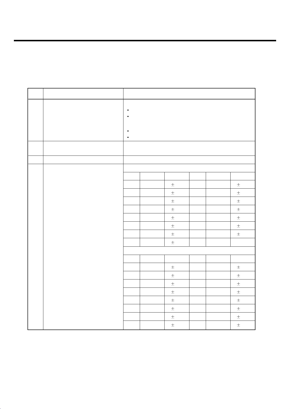
Item Feature Comment
Standard Battery Li-ion, 3.7V 800mAh
Talk time Up to 200min: GSM Tx Level 7
Stand by time Up to 200 hours (Paging Period: 5, RSSI: -85
Charging time Approx. 2.5 hours
RX Sensitivity -102dBm
TX output power
GSM900: 32.5dBm(Level 5),
DCS: 29.5dBm(Level 0)
GPRS compatibility Class 10
SIM card type 3V only
Display
MAIN: TFT 128 × 160 pixel 262K Color
SUB: CSTN 96 × 64 pixel 65K Color
Hard icons. Key Pad
Status Indicator
0 ~ 9, #, *, Up/Down/Left/Right/Ok Navigation Key
Menu Key, Clear Key, Back Key, Confirm Key
Send Key, Volume Key, PWR Key, Camera Key, Hot Key
ANT Internal
EAR Phone Jack Yes (Mono)
PC Synchronization Yes
Speech coding EFR/FR/HR/AMR
Data Yes
Vibrator Yes
Loud Speaker Yes
Voice Recoding Yes
Microphone Yes
Speaker/Receiver One way speaker
Travel Adapter Yes
MIDI SW MIDI (Mono SPK)
Camera VGA CMOS
Bluetooth Bluetooth version 2.0+EDR
- 10 -
2. PERFORMANCE
2.2 Technical Specification
LGE Internal Use Only
Copyright © 2008 LG Electronics. Inc. All right reserved.
Only for training and service purposes
Item Description Specification
GSM900
TX: 890 + 0.2 x (N-1024) MHz (N=975 ~ 1023)
1Frequency Band
RX: 935 + 0.2 x (N-1024) MHz (N=975 ~ 1023)
DCS
TX: 1710.2 + 0.2x(N-512 ) MHz (N=512 ~ 885)
RX: 1805.2 + 0.2x(N-512 ) MHz (N=512 ~ 885)
2 Phase Error
RMS < 5 degrees
Peak < 20 degrees
3 Frequency Error < 0.1 ppm
GSM900
Level Power Toler. Level Power Toler.
5 33 dBm 2dB 13 17 dBm 3dB
6 31 dBm 3dB 14 15 dBm 3dB
7 29 dBm 3dB 15 13 dBm 3dB
8 27 dBm 3dB 16 11 dBm 5dB
9 25 dBm 3dB 17 9 dBm 5dB
10 23 dBm 3dB 18 7 dBm 5dB
11 21 dBm 3dB 19 5 dBm 5dB
4 Power Level 12 19 dBm 3dB
DCS
Level Power Toler. Level Power Toler.
0 30 dBm 2dB 8 14 dBm 3dB
1 28 dBm 3dB 9 12 dBm 4dB
2 26 dBm 3dB 10 10 dBm 4dB
3 24 dBm 3dB 11 8 dBm 4dB
4 22 dBm 3dB 12 6 dBm 4dB
5 20 dBm 3dB 13 4 dBm 4dB
6 18 dBm 3dB 14 2 dBm 5dB
7 16 dBm 3dB 15 0 dBm 5dB
- 11 -
2. PERFORMANCE
LGE Internal Use Only
Copyright © 2008 LG Electronics. Inc. All right reserved.
Only for training and service purposes
Item Description Specification
GSM900
Offset from Carrier (kHz). Max. [dBc]
100 +0.5
200 -30
250 -33
400 -60
600 ~ <1,200 -60
1,200 ~ <1,800 -60
1,800 ~ <3,000 -63
3,000 ~ <6,000 -65
5
Output RF Spectrum 6,000 -71
(due to modulation) DCS
Offset from Carrier (kHz). Max. [dBc]
100 +0.5
200 -30
250 -33
400 -60
600 ~ <1,200 -60
1,200 ~ <1,800 -60
1,800 ~ <3,000 -65
3,000 ~ <6,000 -65
6,000 -73
GSM900
Offset from Carrier (kHz) Max. [dBm]
Output RF Spectrum 400 -19
6
(due to switching transient) 600 -21
1,200 -21
1,800 -24
- 12 -
2. PERFORMANCE
LGE Internal Use Only
Copyright © 2008 LG Electronics. Inc. All right reserved.
Only for training and service purposes
Item Description Specification
DCS
Offset from Carrier (kHz) Max. [dBm]
Output RF Spectrum 400 -22
6
(due to switching transient) 600 -24
1,200 -24
1,800 -27
7 Spurious Emissions Conduction, Emission Status
GSM900
8Bit Error Ratio
BER (Class II) < 2.439% @-102 dBm
DCS
BER (Class II) < 2.439% @-102 dBm
9 RX Level Report Accuracy 3 dB
10 SLR 8 3 dB
Frequency (Hz) Max.(dB) Min.(dB)
100 -12 200 0 300 0 -12
11 Sending Response 1,000 0 -6
2,000 4 -6
3,000 4 -6
3,400 4 -9
4,000 0 -
12 RLR 2 3 dB
Frequency (Hz) Max.(dB) Min.(dB)
100 -12 200 0 300 2 -7
13 Receiving Response
500 * -5
1,000 0 -5
3,000 2 -5
3,400 2 -10
4,000 2
* Mean that Adopt a straight line in between 300 Hz
and 1,000 Hz to be Max. level in the range.
- 13 -
2. PERFORMANCE
LGE Internal Use Only
Copyright © 2008 LG Electronics. Inc. All right reserved.
Only for training and service purposes
Item Description Specification
14 STMR 13 5 dB
15 Stability Margin > 6 dB
dB to ARL (dB) Level Ratio (dB)
-35 17.5
-30 22.5
-20 30.7
16 Distortion -10 33.3
0 33.7
7 31.7
10 25.5
17 Side Tone Distortion Three stage distortion < 10%
18
System frequency
≤2.5 ppm
(13 MHz) tolerance
19 32.768KHz tolerance ≤ 30 ppm
At least 65 dBspl under below conditions:
20 Ringer Volume 1. Ringer set as ringer.
2. Test distance set as 50 cm
21 Charge Current
Fast Charge: < 600 mA
Slow Charge: < 120 mA
Antenna Bar Number Power
5-92 dBm ~
4-100 dBm ~ -93 dBm
22 Antenna Display 3 -101 dBm ~ -100 dBm
2-103 dBm ~ -101 dBm
1-105 dBm ~ -104 dBm
0~ -106 dBm
Battery Bar Number Voltage
Power off 3.33V 0.03 V
23 Battery Indicator
0(blink) 3.54V 0.05 V
13.64V 0.05 V
23.75V 0.05 V
33.76V 0.05 V ~
- 14 -
2. PERFORMANCE
LGE Internal Use Only
Copyright © 2008 LG Electronics. Inc. All right reserved.
Only for training and service purposes
Item Description Specification
24 Low Voltage Warning
3.54 0.05 V (Call) every 1 minutes
3.54 0.05 V (Standby)
25 Forced shut down Voltage 3.33 0.05V
1 Li-ion Battery
26 Battery Type
Standard Voltage = 3.7 V
Battery full charge voltage = 4.2 V
Battery full charge voltage = 4.2 V
Switching-mode charger
27 Travel Charger Input: 100 ~ 240 V, 50/60 Hz
Output: 4.8V ~ 6.4V, 400 mA
- 15 -
3. TECHNICAL BRIEF
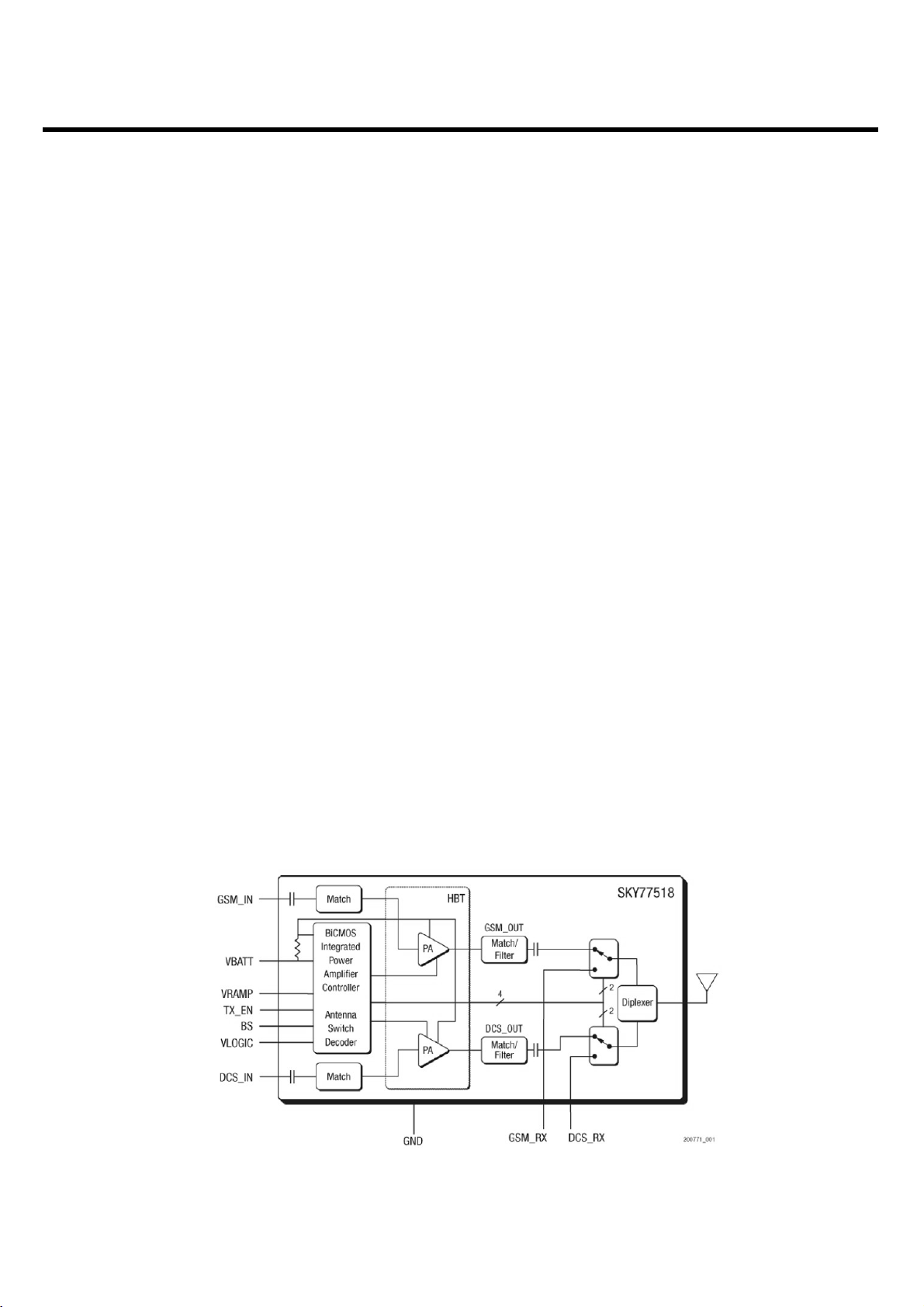
3.1 TX module (SKY77518, U501)
The SKY77518 is a Transmit and receive front-end-module (FEM) with Integrated Power Amplifier
Control (iPAC) for dual-band cellular handsets comprising GSM900 and DCS operation. Designed in a
low profile, compact form factor, the SKY77518 offers a complete Transmit VCO-to-Antenna and
Antenna-to-Receive SAW filter solution. The FEM also supports class 12 General Packet Radio
Service (GPRS) multi-slot operation.
The module consists of a GSM900 PA block and a DCS PA block, impedance-matching circuitry for 50
ohm input and output impedances, TX harmonics filtering, high linearity and low insertion loss PHEMT
RF switches, diplexer and a Power Amplifier Control (PAC) block with internal current sense resistor. A
custom BiCMOS integrated circuit provides the internal PAC function and decoder circuitry to control
the RF switches. The two Heterojunction Bipolar Transistor (HBT) PA blocks are fabricated onto a
single Gallium Arsenide (GaAs) die. One PA block supports the GSM900 band and the other PA block
supports the DCS band. Both PA blocks share common power supply pads to distribute current. The
output of each PA block and the outputs to the two receiver pads are connected to the antenna pad
through PHEMT RF switches and a diplexer. The GaAs die, PHEMT die, Silicon (Si) die and passive
components are mounted on a multi-layer laminate substrate. The assembly is encapsulated with
plastic overmold.
Band selection and control of transmit and receive modes are performed using two external control
pads. Refer to the functional block diagram in Figure 3.1 below. The band select pad (BS) selects
between GSM and DCS modes of operation. The transmit enable (TX_EN) pad controls receive or
transmit mode of the respective RF switch (TX = logic 1). Proper timing between transmit enable
(TX_EN) and Analog Power Control (VRAMP) allows for high isolation between the antenna and
TX_VCO while the VCO is being tuned prior to the transmit burst.
The SKY77518 is compatible with logic levels from 1.2V to VCC for BS and TX_EN pads, depending
on the level applied to the VLOGIC pad. This feature provids additional flexibility for the designer in the
selection of FEM interface control logic.
3. TECHNICAL BRIEF
LGE Internal Use Only
Copyright © 2008 LG Electronics. Inc. All right reserved.
Only for training and service purposes
Figure 3.1 Functional Block Diagram
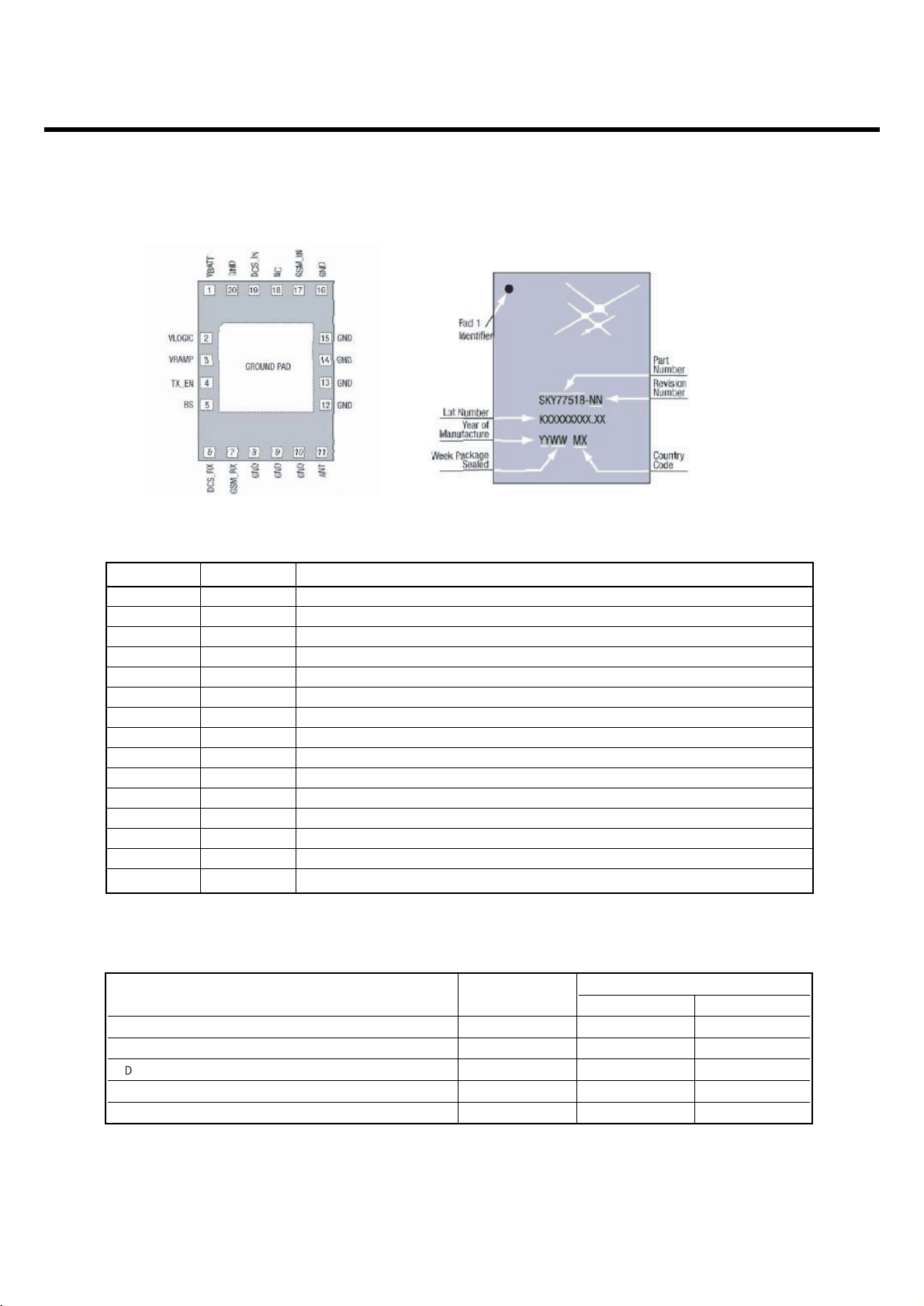
Pin Mame Description
1 VCATT Battery input voltage
2 VLOGIC Control logic level selection/Standby control
3VRAMP Analog power control voltage input
4 TX_EN TX/RX select (mode control)
5BSBand Select (mode control)
6 DCS_RX DCS Receive RF Output (1805-1880 MHz)
7 GSM_RX GSM Receive RF Output (920-960 MHz)
8-10 GND RF and DC Ground
11 ANT RF_IN/RF_OUT to Antenna
12-16 GND RF and DC Ground
17 GSM_IN RF input 880-915 MHz
18 NC No Connect
19 DCS_IN RF input 1710-1785 MHz
20 GND RF and DC Ground
GMD PADS GROUND GRID Ground Pads, module underside
Mode V
LOGIC
Input Control Bits
TX_En BS
STANDBY 0 X1 X1
GSM_RX 1 0 0
CS_RX 1 0 1
GSM_TX 1 1 0
DCS_TX 1 1 1
LGE Internal Use Only
Copyright © 2008 LG Electronics. Inc. All right reserved.
Only for training and service purposes
3. TECHNICAL BRIEF
- 16 -
Table 3.1 Pad description
Table 3.2 Mode Control logic
Figure 3.2 Pad configuration (Top view) and case marking
- 17 -
3. TECHNICAL BRIEF
3.2 Transceiver (AD6548, U502)
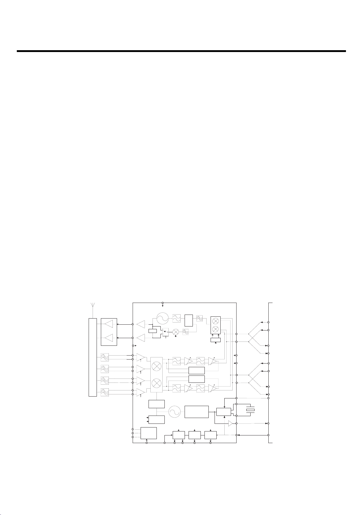
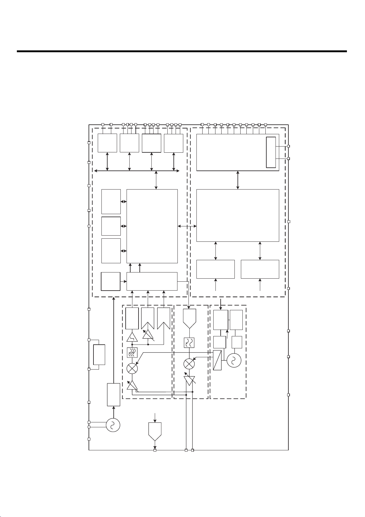
The AD6548 provides a highly integrated direct conversion radio solution that combines, on a single chip, all radio
and power management functions necessary to build the most com-pact GSM radio solution possible. The only
external components required for a complete radio design are the Rx SAWs, PA, Switchplexer and a few passives
enabling an extremely small cost effective GSM Radio solution. The AD6548 uses the industry proven direct
conversion receiver architecture of the OthelloTM family. For Quad band applications the front end features four
fully integrated programmable gain differential LNAs. The RF is then down converted by quad-rature mixers and
then fed to the baseband programmable-gain amplifiers and active filters for channel selection. The Receiver
output pins can be directly connected to the baseband analog processor. The Receive path features automatic
calibration and tracking to remove DC offsets. The transmitter features a translation-loop architecture for directly
modulating baseband signals onto the integrated TX VCO.
The translation-loop modulator and TX VCO are extremely low noise removing the need for external SAW filters
prior to the PA. The AD6548 uses a single integrated LO VCO for both the receive and the transmit circuits. The
synthesizer lock times are optimized for GPRS applications up to and including class 12.
AD6548 incorporates a complete reference crystal calibration system. This allows the external VCTCXO to be
replaced with a low cost crystal. No other external components are required. The AD6548 uses the traditional
TCXO reference source. The AD6548 also contains on-chip low dropout voltage regulators (LDOs) to deliver
regulated supply voltages to the functions on chip, with a battery input voltage of between 2.9V and 5.5V.
Comprehensive power down options are included to minimize power consumption in normal use. A standard 3
wire serial interface is used to program the IC. The interface features low-voltage digital interface buffers
compatible with logic levels from 1.6V to 2.9V.
LGE Internal Use Only
Copyright © 2008 LG Electronics. Inc. All right reserved.
Only for training and service purposes
Figure 3.3 AD6548 Block Diagram
Antenna Switch Module
DC Offset
Correction
DC Offset
Correction
PFD
/2
LDO
Reg 3
LDO
Reg 2
LDO
Reg 1
Frac-N Synth
RX LO
Generator
TX LO
Generator
Xtal Osc
+ Tuning
Serial
Interfac
e
/4
SEN
SCLK
SDATA
RX1900B
RX1900
RX1800B
RX1800
RX900B
RX900
RX850B
RX850
TXOP_HI
TXOP
_LO
VDD
VBAT VLDO3 VLDO2 VLDO1
LO VCO
Suppl
y
REF_OP
REFIN
REFINB
VAFC
VCC_REF
Q
QB
I
IB
VCC_BBI
VCC_B
BQ
LNA Gain
Reductio
n
TX_LO2
TX_LO1
TX_LO
2
TX_LO
1
General
Suppl
y
TX circuits
supply
CLK
RXQB
RXQ
TXQB
TXQ
RXIB
RXI
TXI
TXI
B
AFC
REF_OP
Band
Control
TX Loop
Filt
er
GSM1800/1900
GSM850/
900
PA Module
AD6548
VCC_FE
VCC_TXVCO
Ref
Suppl
y
VCC_
TXVCO
LGE Internal Use Only
Copyright © 2008 LG Electronics. Inc. All right reserved.
Only for training and service purposes
Notes:
1. Supply regulated by internal LDO3 and should not be connected to any other supply
2. Internally connected as Synth supply (Counters + SDM + Charge pump)
3. Supply regulated by internal LDO2 and should not be connected to any other supply
3. TECHNICAL BRIEF
- 18 -
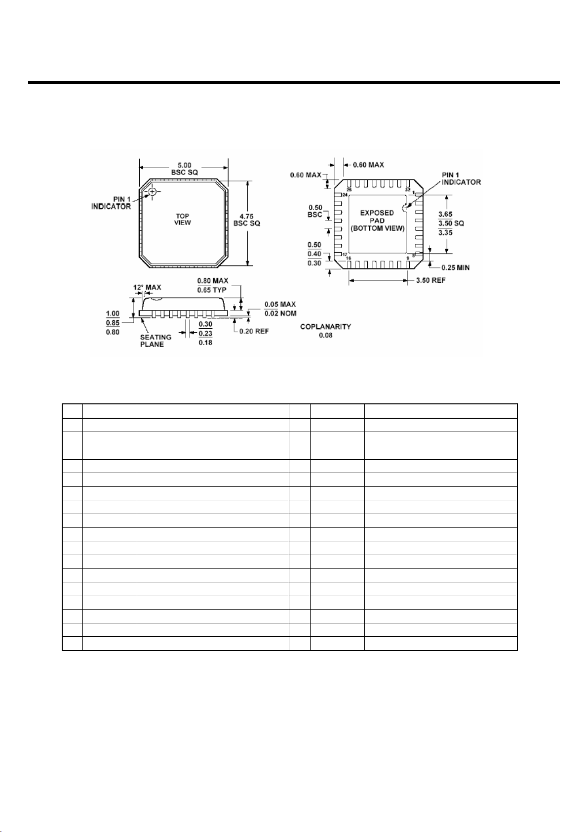
Table 1 AD6548/9 Pin Descriptions
No Name Description No Name Description
1 VCC_FE Front end supply (IP) 17 VCC_REF Reference Oscillator Supply (IP)
2I I baseband input/output 18
VAFC/ AD6548 Crystal Freq control (IP)
N/C AD6549: Spare Pin
3IBI baseband input/output 19 REFIN Crystal Connection
4 VCC_BBI Baseband I, TX path supply (IP) 20 REFINB Crystal Connection
5 SDATA Serial port data 21 REF_OP Reference Frequency Output
6 SCLK Serial port clock 22 QB Q baseband input/output
7 SEN Serial port enable 23 Q Q baseband input/output
8 N/C Not connected 24 VCC_BBQ Baseband Q supply (IP)
9 VLDO3 TX LDO Output (1) 25 RX1900B PCS 1900 LNA input
10 TXOP_LO Transmit O/P (850/900MHz) 26 RX1900 PCS 1900 LNA input
11 TXOP_HI Transmit O/P (1800/1900MHz) 27 RX1800B DCS 1800 LNA input
12 VCC_TXVCO TX VCO supply (1) 28 RX1800 DCS 1800 LNA input
13 VDD Serial interface supply 29 RX900B E-GSM LNA input
14 VBAT Battery I/P for LDO reg’s 30 RX900 E-GSM LNA input
15 VLDO1 LDO regulator Output (2) 31 RX850B GSM 850 LNA input
16 VLDO2 LO VCO Supply (3) 32 RX850 GSM 850 LNA input
GOMPLIANT TO JEDEC STANDARDS MO-220-VHHD-2
- 19 -
3. TECHNICAL BRIEF
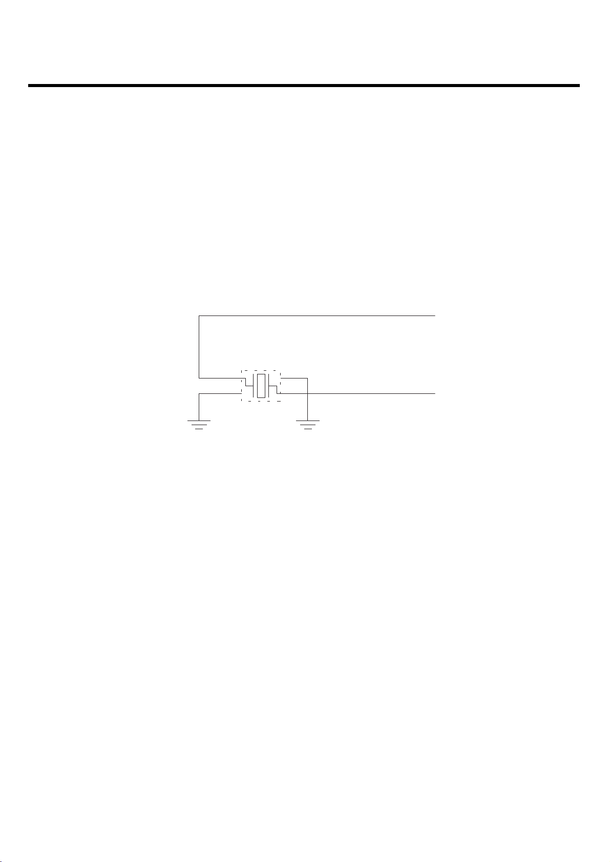
3.3 26 MHz Clock (Crystal, X500)
The 26 MHz clock (X500) consists of a TCXO (Crystal Oscillator) which oscillates at a frequency of 26 MHz. The
AD6548 requires only an external low cost crystal as the frequency reference. The circuitry to oscillate the crystal
and tune its frequency is fully integrated. The Oscillator is a balanced implementation requiring the crystal to be
connected across 2 pins. There is a programmable capacitor array included for coarse tuning of fixed offsets (e.g.
crystal manufacturing tolerance), and an integrated varactor for dynamic control. The oscillator is designed for use
with a 26MHz crystal. Dedicated control software ensures excellent frequency stability under all circumstances.
LGE Internal Use Only
Copyright © 2008 LG Electronics. Inc. All right reserved.
Only for training and service purposes
Figure 3.4 CRYSTAL CIRCUIT DIAGRAM
X500
34
12
26MHz
TSX-3225_26MHZ
- 20 -
3. TECHNICAL BRIEF
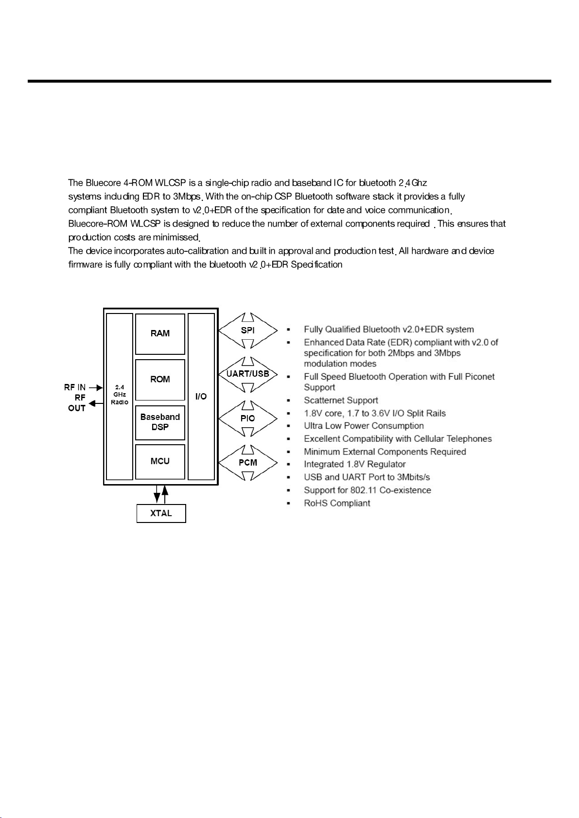
3.4 B/T Chip (Bluecore 4-ROM WLCSP, U401)
LGE Internal Use Only
Copyright © 2008 LG Electronics. Inc. All right reserved.
Only for training and service purposes
System Architecure Device Features
- 21 -
3. TECHNICAL BRIEF
LGE Internal Use Only
Copyright © 2008 LG Electronics. Inc. All right reserved.
Only for training and service purposes
SPI_CSB
SPI_CLK
SPI_MOSI
USB_DP
USB_DN
SPI_MISO
UART_TX
UART_RX
UART_RTS
UART_CTS
PCM_OUT
PCM_IN
PCM_SYNC
PCM_CLK
PIO[1]
PIO[0]
PIO[2]
PIO[3]
PIO[4]
PIO[5]
PIO[6]
PIO[7]
PIO[8]
PIO[9]
PIO[10]
VDD_USB
VDD_PIO
TEST_EN
RESETB
VDD_PAD S
VDD_ CORE
VDD_ANA
VREG_IN
VDD_LO
USB
RAM
Baseband and Logic
Mapped
Memory
Internal
Mode
Burst
Control
ROM
Serial
Interface
Synchro nous
s
Statu
r
Controlle
RT
UA
Unit
Memory
Management
Layer
Physical
Hardware
Interface
Audio PC M
r
Interrupt
e
Engin
Controlle
Micro controller
r
ADC
ADC
Demod ulato
ATTENUATO
R
Out
VREG
In
IQ DEMOD
A
LN
n
Clock
Generatio
RSSI
RF Receiver
C
DA
D
IQ MO
PA
RF
/N/
5
+4
-45
RF Transmitter
O
AIO
Programm able I/
r
RISC
Microc ontrolle
r
Event
Time
r
r
Loop
Filte
Synt hesis e
1
N+
Fref
Tune
AIO[0]
AIO[2]
VSS_ PADS
VSS_DIG
VSS_ANA
VSS_LO
RF Synt hesiser
VSS_RADIO
XTAL_OUT
XTAL_IN
VDD_ RADIO
C
AUX
DA
AUX_DAC
RF_A
RF_B

- 22 -
3. TECHNICAL BRIEF
LGE Internal Use Only
Copyright © 2008 LG Electronics. Inc. All right reserved.
Only for training and service purposes
3.5 Baseband Processor (AD6724, U104)
• AD6724 is an ADI designed processor
• AD6724 consists of
FEATURES-DIGITAL
Complete Integrated Programmable Digital
Baseband Processor divided into three main
subsystems:
Control Processor Subsystem including:
• 32-bit MCU ARM7TDMI® Control Processor
• 39 MHz operation at 1.8V
• 1Mb of on-chip System SRAM Memory
DSP Subsystem including:
• 16-bit Fixed Point DSP Processor
• 91 MIPS[1] at 1.8V
• Data and Program SRAM
• Program Instruction Cache
• Full Rate, Enhanced Full Rate and Half Rate
Speech Encoding/Decoding
• Capable of Supporting AMR & PDC Speech
Algorithms
Peripheral Subsystem including:
• Shared Peripheral Bus and Interface
Peripherals
Peripheral Functions
• Parallel and Serial Display Interface
• Keypad Interface
• Flash Memory Interface
• Page-Mode Flash Support
• 1.8V and 3.0V, 64 kbps SIM Interface
• Universal System Connector Interface
• Data Services Interface
• Battery Interface (e.g. Dallas)
Control of Radio Subsystem
Three independent programmable backlight
outputs
Real Time Clock with Alarm
Programmable Power Management and Clock
Management Supports 13 MHz and 26 MHz
Input Clocks
Slow Clocking Scheme for Low Idle Mode
Current Power Down modes
On-chip support for GSM Data Services up to
14.4Kbits/sec, GPRS, HSCSD and IrDA
JTAG Interface for Test and In-Circuit Emulation
FEATURES-ANALOG
Baseband Transmit Section
• GMSK Modulator
• I-channel & Q-channel Transmit DACs and
Filters
• Power Ramping DAC
Baseband Receive Section
• I-channel and Q-channel Receive ADCs and
Filters
Auxiliary Section
• Voltage Reference
• Automatic Frequency Control DAC
• Auxiliary ADC
• Light Controllers
Audio Section
• 8 kHz & 16 kHz Voiceband Codec
• 48 kHz Monophonic DAC
• Power Amplifiers
Poer Management Section
• Voltage Regulators
• Battery Charger
• Battery Protection
264-Ball package (17x17 grid), 12x12mm,
0.65mm ball pitch
APPLICATIONS
GSM850/GSM900/DCS1800/PCS1900 Wireless
Terminals GSM Phase 2 Compliant
- 23 -
3. TECHNICAL BRIEF
LGE Internal Use Only
Copyright © 2008 LG Electronics. Inc. All right reserved.
Only for training and service purposes
Figure 3.5 SYSTEM INTERCONECTION OF AD6721 EXTERNAL INTERFACE
- 24 -
3. TECHNICAL BRIEF
3.5.1 Interconnection with external devices
A. RTC block interface
Countered by external X-TAL
The X-TAL oscillates 32.768KHz
B. LCD module interface
The LCD module is basically controlled by DBB, Mobile Media Processor AIT701G is just controlling
the path which is LCD line or Camera line.
If AIT701G is in the state of by-pass mode, the LCD control signals from AD6724 are by-passed
through AIT701G.
In operating mode, the AIT701G controls the camera module directly.
LGE Internal Use Only
Copyright © 2008 LG Electronics. Inc. All right reserved.
Only for training and service purposes
Signals Description
L_MAIN_LCD_CS MAIN LCD driver chip enable. MAIN LCD driver IC has own CS
pinL_SUB_LCD_CS SUB LCD driver chip enable. SUB LCD driver IC has own CS pin
LCD_ID Select LCD module maker(2.8V: SHARP, 0V: LGIT)
LCD_RESET This pin resets LCD module. This signal comes from AD6721 directly.
LCD_WR Enable writing to LCD Driver.
LCD_RD Enable reading to LCD Driver.
LCD_RS
This pin determines whether the data to LCD module are display
data or control data. LCD_RS can select 16 bit parallel bus.
2V8_CAM 2.8V voltage is supplied to LCD driver IC.
IF_MODE
Select 16bits or 8bits interface mode for MAIN LCD.
For the future
Table 3.5.B LCD CONTRON SIGNALS DISCRIPTION
- 25 -
3. TECHNICAL BRIEF
LGE Internal Use Only
Copyright © 2008 LG Electronics. Inc. All right reserved.
Only for training and service purposes
The backlight of LCD module is controlled by AD6724 via AAT3155.
The control signals related to Backlight LED are given bellow.
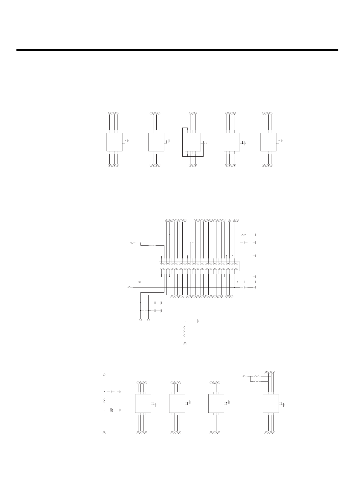
C. RF interface
The AD6724 control RF parts through PA_BAND, ANT_SW, PA_EN, S_EN, S_DATA, S_CLK
Signals Description
MLED Current source for backlight LED
LCD_DIM_CTRL Control LCD backlight level in 16 steps
MLED[1:4] This pins are returned-paths for backlight LED current source (MLED)
Table 3.5.B2 DESCRIPTION OF LCD BACKLIGHT LED CONTROL
Signals Description
PA_BAND (GPO 3) PAM Band Select
ANT_SW (GPO 9) Antenna switch Band Select
PA_EN (GPO11) PAM Enable/Disable
S_EN (GPO 19) PLL Enable/Disable
S_DATA (GPO 20) Serial Data to PLL
S_CLK (GPO 21) Clock to PLL
Table 3.4.C RF CONTROL SIGNALS DESCRIPTION
- 26 -
3. TECHNICAL BRIEF
D. SIM interface
The AD6721 provides SIM Interface Module. The AD6721 checks status periodically during
established call mode whether SIM card is inserted or not, but it doesn't check during deep Sleep
mode. In order to communicate with SIM card, 3 signals SIM_DATA, SIM_CLK,
SIM_RST(GPIO_23) are required. The descriptions about the signals are given by bellow Table 3-5
in detail.
LGE Internal Use Only
Copyright © 2008 LG Electronics. Inc. All right reserved.
Only for training and service purposes
Signals Description
SIM_DATA
This pin receives and sends data to SIM card.
This model can support 3.0 volt and 1.8 volt interface SIM card.
SIM_CLK Clock 3.25MHz frequency.
SIM_RST
Reset SIM block
(GPIO_23)
Table 3.5.D SIM CONTROL SIGNALS DESCRIPTION
Figure 3.5.D2 SIM Interface of AD6724
2V85_VSIM
1
2
3
7
89
C318
220n
R338
0
2V85_VSIM
R337
15K
C317
NA
J300
4
C5
5
C6
6
C7
10
GND4
GND3
C1
C2
C3
GND1
GND2
C319
NA
SIM_RST
SIM_CLKSIM_DATA
C320
1000p

- 27 -
3. TECHNICAL BRIEF
LGE Internal Use Only
Copyright © 2008 LG Electronics. Inc. All right reserved.
Only for training and service purposes
E. LDO Block
There are8 LDOs in the AD6724.
- 1V8_VCORE: supplies Digital baseband Processor core and AD6721 digital core(1.8V, 80mA)
- 2V8_VMEM: supplies external memory and the interface to the external memory on the digital
baseband processor (2.8V, 150mA)
- 2V8_VEXT: supplies Radio digital interface and high voltage interface (2.8V, 200mA)
- 2V85_VSIM: supplies the SIM interface circuitry on the digital processor and SIM card
(2.85V,1.8V, 20mA)
- 1V8_VRTC: supplies the Real-Time Clock module (1.8 V, 20 •ÏA)
- 2V5_VMIC: supplies the microphone interface circuitry (2.5 V, 2 mA)
- 2V75_VVCXO: supplies the voltage controlled crystal oscillator ( 2.75 V, 10 mA)
-2V75_VABB: analog basand relulator
- 28 -
3. TECHNICAL BRIEF
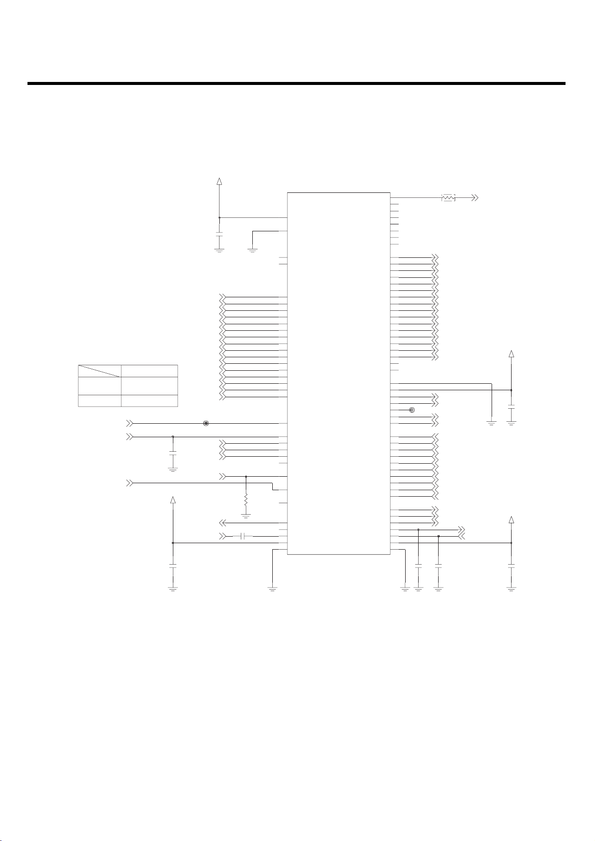
3.6 Display and Interface
Controlled by L_MAIN_LCD_CS, L_SUB_LCD_CS, LCD_RESET, LCD_RS, LCD_WR, LCD_RD,
LCD_IF, L_DATA[00: 15] ports
• L_MAIN_LCD_CS: MAIN LCD driver chip enable. MAIN LCD driver IC has own CS pin
• LCD_RESET: This pin resets LCD module. This signal comes from AD6721 directly.
• LCD_RS: This pin determines whether the data to LCD module are display data or control data.
• LCD_WR: Write control Signal
• LCD_RD: Read control Signal. But this pin used only for debugging.
• L_DATA[00:15]: Parallel data lines.
• LCD_ID: LCD type selection signals
- LCD_ID: LCD maker(0V for LGIT, 2.8V for Sharp)
• For using 262K color, data buses should be 16 bits.
LGE Internal Use Only
Copyright © 2008 LG Electronics. Inc. All right reserved.
Only for training and service purposes
Properties Spec. Unit
Active Screen Size 33.8mm(W) x 46.24mm(H) mm
Color Depth 262K TFT colors
Resolution 128 x RGB x 160 dots
• Main LCD
Properties Spec. Unit
Active Screen Size 18.902mm(W) x 13.43mm(H) mm
Color Depth 65K CSTN colors
Resolution 96 x 64 dots
• Sub LCD
- 29 -
3. TECHNICAL BRIEF
LGE Internal Use Only
Copyright © 2008 LG Electronics. Inc. All right reserved.
Only for training and service purposes
Figure 3.6 LCD INTERFACE CIRCUIT
(
)
L_SUB_LCD_CS
LCD_WR
L_MAIN_LCD_CS
LCD_RS
L_DATA15
L_DATA14
L_DATA13
L_DATA12
L_DATA02
L_DATA01
L_DATA00
C_MCLK
C_PCLK
C_HS
C_CD01
C_CD00
C_CD02
C_CD03
C_VS
(100ohm, 15pF)
ICVE10184E150R101FR
9
8
7
6
G2
INOUT_B1
INOUT_B2
INOUT_B3
INOUT_B4
10
G1
FL600
INOUT_A1
INOUT_A2
1
2
LCD_WR_OUT
L_SUB_LCD_CS_OUT
5
INOUT_A3
INOUT_A4
3
4
LCD_RS_OUT
L_MAIN_LCD_CS_OUT
FL602
2V8_AIT_BT
(LCD/CAM POWER)
2V8_AIT_BT
1V8_AIT_CORE
(SOCKET, 60pin, 0.4mm pitch, 1.0T, ENBY0036801)
(CAMERA CORE POWER)
47p
C601
SPK_RCV_P
9
8
INOUT_B1
INOUT_B2
INOUT_A1
INOUT_A2
1
2
L_DATAOUT15
L_DATAOUT14
100K
R601
C602
C603
SPK_RCV_N
ICVE10184E150R101FR
7
6
G2
INOUT_B3
INOUT_B4
10
G1
5
INOUT_A3
INOUT_A4
3
4
L_DATAOUT13
L_DATAOUT12
LCD_ID
(LCD_RD)
1
CN600
27p
27p
(100ohm, 15pF)
IF_MODE
LCD_WR_OUT
LCD_RS_OUT
L_MAIN_LCD_CS_OUT
5556575859660
789
L_DATAOUT09
L_DATAOUT10
L_DATAOUT08
FL604
L_DATAOUT15
L_DATAOUT11
(100ohm, 15pF)
ICVE10184E150R101FR
1
2
3
4
5
G1
INOUT_A1
INOUT_A2
INOUT_A3
INOUT_A4
10
G2
INOUT_B1
INOUT_B2
INOUT_B3
INOUT_B4
9
8
7
6
L_DATAOUT02
L_DATAOUT00
L_DATAOUT01
L_DATAOUT14
L_DATAOUT13
10
L_DATAOUT12
L600
L_DATAOUT01
L_DATAOUT02
LCD_RESET
L_SUB_LCD_CS_OUT
L_DATAOUT00
L_DATAOUT03
11121314151617181922021222324
MLED
MLED2
MLED3
MLED4
MLED1
L_DATAOUT07
L_DATAOUT05
LCD_VSYNC_OUT
L_DATAOUT06
1u
C604
100nH
L_DATAOUT04
C_CD04_OUT
C_CD03_OUT
41424344454647484955051525354
39440
C_CD06_OUT
C_CD07_OUT
C_CD05_OUT
INOUT_A1
FL606
INOUT_B1
C_CD00_OUT
C_CD01_OUT
C_CD00_OUT
C_CD02_OUT
262728
25
C_SDA_IN
C_VS_OUT
C_HS_OUT
1
2
3
INOUT_A2
INOUT_A3
INOUT_A4
INOUT_B2
INOUT_B3
INOUT_B4
9
8
7
C_CD01_OUT
C_CD02_OUT
C_CD03_OUT
C_PCLK_OUT
C_MCLK_IN
32333435363738
29330 31
C_SCL_IN
C_RST_OUT
(50ohm, 15pF)
ICVE10184E150R500FR
4
5
G1
10
G2
6
CAM_PWR_EN
100K
R602
1u
C607
1u
C606C605
1u
9
8
INOUT_B1
INOUT_B2
FL607
INOUT_A1
INOUT_A2
1
2
C_MCLK_IN
C_PCLK_OUT
7
6
INOUT_B3
INOUT_B4
INOUT_A3
INOUT_A4
3
4
C_VS_OUT
C_HS_OUT
G2
G1
(50ohm, 15pF)
ICVE10184E150R500FR
10
5
128x160 TFT(MAIN) , 96x64 CSTN(SUB) LCD CONNECTOR with VGA CAMERA
LCD_RESET
L_DATAOUT11
L_DATAOUT10
L_DATAOUT09
L_DATAOUT08
47p
C600
R600
100ohm
1
2
INOUT_A1
INOUT_A2
FL601
INOUT_B1
INOUT_B2
8
9
3
INOUT_A3
INOUT_B3
7
4
INOUT_A4
INOUT_B4
6
5
G1
10
G2
VA600
EVL14S02200
ICVE10184E150R101FR
L_DATA11
L_DATA10
L_DATA09
nLCD_RESET
L_DATA08
FL603
(100ohm, 15pF)
L_DATAOUT04
L_DATAOUT06
L_DATAOUT05
L_DATAOUT07
9
8
7
INOUT_B1
INOUT_B2
INOUT_B3
INOUT_B4
INOUT_A1
INOUT_A2
INOUT_A3
INOUT_A4
1
2
3
L_DATA04
L_DATA06
L_DATA07
L_DATA05
MOTOR(+)
6
G2
10
G1
5
4
ICVE10184E150R101FR
(100ohm, 15pF)
C_CD04_OUT
C_CD05_OUT
9
8
INOUT_B1
INOUT_B2
FL605
INOUT_A1
INOUT_A2
1
2
C_CD04
C_CD05
C_CD06_OUT
C_CD07_OUT
7
6
G2
INOUT_B3
INOUT_B4
G1
INOUT_A3
INOUT_A4
3
4
C_CD06
C_CD07
10
5
(50ohm, 15pF)
ICVE10184E150R500FR
2V8_AIT_BT
L_DATAOUT03
C_SCL_IN
C_SDA_IN
4.7K
R604
4.7K
R603
2
3
4
1
5
G1
INOUT_A3
INOUT_A4
INOUT_A1
INOUT_A2
10
G2
FL608
INOUT_B1
INOUT_B2
INOUT_B3
INOUT_B4
9
8
7
6
C_RST C_RST_OUT
C_SCK
C_SDA
L_DATA03
50ohm, 15pF
ICVE10184E150R500FR

- 30 -
3. TECHNICAL BRIEF
3.7 Camera Interface(AIT701G , U402)
This model has a built-in VGA(640 x 320) camera module. And the camera produces JPG pictures.
Camera module is controlled by AIT701G. Interface is done by I2C and YUV format. I2C is a control
signal and YUV is real data interface signal.
LGE Internal Use Only
Copyright © 2008 LG Electronics. Inc. All right reserved.
Only for training and service purposes
Figure 3.7.2 SENSOR CHIP BLOCK DIAGRAM
Figure 3.7.1 AIT701G BLOCK DIAGRAM
- 31 -
3. TECHNICAL BRIEF
LGE Internal Use Only
Copyright © 2008 LG Electronics. Inc. All right reserved.
Only for training and service purposes
Figure 3.7.3 AIT701G CIRCUIT
HIGH
LOW
AIT_BYPASS
_MAIN_LCD_CS
_SUB_LCD_CS
AIT_BYPASS
BYPASS MODE
(MAIN, SUB LCD)
CAMERA MODE
2V8_AIT_BT
C409
NA
C416
1u
1V8_AIT_CORE
C402
0.01u
DATA00
DATA01
DATA02
DATA03
DATA04
DATA05
DATA06
DATA07
DATA08
DATA09
DATA10
DATA11
DATA12
DATA13
DATA14
DATA15
AIT_BYPASS
nRD
nWR
ADD01
nAIT_RESET
AIT_13M
R404
100K
C415
1000p
U402
PGPIO0
PGPIO1
H5
VDD_CORE
H6
GND_CORE
D3
PSCAN_EN
E10
PTEST_EN
J3
PHD0
H3
PHD1
K4
PHD2
J4
PHD3
K5
PHD4
J5
PHD5
K6
PHD6
J6
PHD7
K10
PHD8
J9
PHD9
H10
PHD10
H9
PHD11
G10
PHD12
G9
PHD13
G8
PHD14
F10
PHD15
K7
PHLCD_BY
K1
PHCS_
J1
PHRD_
K2
PHWE_
J7
PHLCD_A0
J8
PHINT
K3
PRST_
K8
PHLCD2_CS_
J10
PHGPIO_CS_
F2
PS_RST_
K9
PHWAIT_
J2
PMCLK PPXL_CLK
G3 H8
VDD_IO0
H4
GND_IO0 GND_IO1
AIT701G
EUSY0318501
PGPIO2
PGPIO3
PGPIO4
PGPIO5
PGPIO6
PGPIO7
PLCD0
PLCD1
PLCD2
PLCD3
PLCD4
PLCD5
PLCD6
PLCD7
PLCD8
PLCD9
PLCD10
PLCD11
PLCD12
PLCD13
PLCD14
PLCD15
PLCD16
PLCD17
GND_IO2
VDD_IO2
PLCD2_CS_
PLCD1_CS_
PLCD_RD_
PLCD_A0
PLCD_WE_
PHSYNC
PVSYNC
PD0
PD1
PD2
PD3
PD4
PD5
PD6
PD7
PSEN
PSDA
PSCK
PDCLK
VDD_IO1
E9
D9
C10
B9
A7
B7
F9
D10
A10
B10
A9
C9
D8
A8
B8
C8
C7
C6
B6
C5
B5
A6
C4
A5
B4
C3
F8
E8
A2
B2
A3
B3
A4
E3
G1
E2
E1
D1
D2
C2
C1
A1
B1
H1
H2
G2
F3
F1
H7
LCD_RD
C417
NA
R401
0
L_DATA00
L_DATA01
L_DATA02
L_DATA03
L_DATA04
L_DATA05
L_DATA06
L_DATA07
L_DATA08
L_DATA09
L_DATA10
L_DATA11
L_DATA12
L_DATA13
L_DATA14
L_DATA15
L_SUB_LCD_CS
L_MAIN_LCD_CS
LCD_RS
LCD_WR
C_HS
C_VS
C_CD00
C_CD01
C_CD02
C_CD03
C_CD04
C_CD05
C_CD06
C_CD07
CAM_PWR_EN
C_SDA
C_SCKC_RST
C_MCLK
C_PCLK
C418
NA
LCD_VSYNC_OUT
2V8_AIT_BT
C407
2V8_AIT_BT
C419
1u
1u
 Loading...