

Page 1

Service Manual
Internal Use Only
Service Manual
KP220
Model : KP220
Date: March, 2008 / Issue 1.0
Page 2

AMENDMENT RECORD
AMENDMENT RECORD SHEET
Issue Number Date
Draft 1.00 29.11.2007
Draft 1.2 14.02.2008
Draft 1.3 18.02.2008
For details of previous history refer to archival documents.
New Issue Number – Date Changes This Issue, Page and Description Remarks
Draft 1.00 29.11.2007 All for Publication
First draft
Issue
Draft 1.2 14.02.2008 All for Publication
Draft 1.3 18.02.2008
All for Publication
Second
draft Issue
Third draft
Issue
KP220 SERVICE MANUAL V1.2
Page 3

Next Section >>
Main Menu
SECTION 1
1
Introduction
KP220 SERVICE MANUAL V1.2
Page 4

1. Introduction
The variation of “KP220” is shown below.
This Service Manual is indicated for 7338.
Variation Note.
Product Code Trade Name
7338
XXXXXXXX KP220
KP220 SERVICE MANUAL V1.2
Page 5

This is the Electronic Service Manual for KP220 Triple Band GSM Digital
Cellular Telephone from LG. It contains specific information on repair and test
procedures.
For details of user functions, general operation and installation, please refer to the
User Guide.
The Service Manual is set out in the following sections.
1. Precautions for Repair Work : provides general guidelines for
undertaking safe and efficient repair work.
2. Unit Specification: provides the technical specifications for
KG195 Triple Band GSM Digital Cellular Telephone.
3. Introduction of Service Level :
a)
Service Level 1:describes definition of Service Level 1, equipment and
tools required for this level.
b)
Service Level 2 :describes definition, equipment and tools required for
Service Level 2.
4. Circuit Description: provides functional details of the circuits, block
diagrams and component purpose descriptions.
5.
Servicing : defines the jigs, fixtures and test configurations required for
servicing the product; and describes the processes of assembly and
disassembly.
6.
Troubleshooting : provides an aid to fault finding the product. Includes,
using the signal levels and plots at various parts of the circuit.
7. Device Information : provides functional information and pin-outs of
most of the semiconductor devices within the HHP.
8. Glossary :
terms used in this GSM and this manual.
KP220 SERVICE MANUAL V1.2
Page 6

Next Section >>
Main Menu
SECTION 2
2
Precautions
for Repair Work
KP220 SERVICE MANUAL V1.2
Page 7

PRECAUTION
Important
Please read the following cautions, notes and
warnings before progressing through this manual or
undertaking any repair action.
Remember: SAFETY FIRST!
CAUTION:
AC Power Cord:
Care must be taken not to damage the AC power cord as fire or electric shock may
result.
Battery Pack:
Only use the specified batteries and chargers with this equipment.
Do not short the battery terminals together.
Keep the battery pack away from fire and sources of ignition.
Remember to recharge the battery pack after each use.
Before Powering up the Equipment:
• Only switch on the telephone’s power once the test or installation set-up is
complete.
• Switching on at the wrong time may result in electric shock or damage to system
components.
• Always ensure that the power is switched off before making connections /
disconnection’s.
• It is important to check that the correct DC voltage is applied to the equipment to
prevent electrical damage.
Component Polarity:
Always check the polarity of connections and components before soldering.
Particular attention must be paid to IC.s, diodes, transistors, capacitors and any
other semiconductor device that is polarity dependent.
KP220 SERVICE MANUAL V1.2
Page 8

Electrostatic Damage (ESD):
Semiconductor devices are easily damaged by electrostatic discharge. Many of the
procedures detailed in this manual involve disassembly of the equipment and
therefore handling of the printed circuit boards.
To protect these devices from ESD a wrist strap connected to ground must be worn.
In addition to this the work surface must be covered with an anti-electrostatic mat,
which should also be grounded.
If printed circuit boards are to be stored without being re-assembled into their
equipment, then they must be kept in an anti-electrostatic bag.
Grounding:
Each piece of test equipment should be electrically grounded. A third (grounding)
pin is provided as a safety feature. Ensure that the electrical outlet also contains
this feature.
Cosmetic Protection during Repair Work:
Always ensure that the working surface is kept clean and free from abrasive
materials.
The LCD is very susceptible to scratches and damage. It should be covered with
clear adhesive vinyl while the equipment is disassembled.
Storage of Faulty Components:
Any components that are replaced due to failure should be kept safely in an antielectrostatic container. NEC’s Quality or Research & Development Departments
may require them to make quality and reliability investigations.
No Fault Found Equipment:
In some cases the reported symptom may not be apparent. You may subject the
equipment to a controlled amount of stress, vibration and temperature variation to
see if the fault occurs.
Care should be taken not to apply excessive stress or vibration or extreme
temperature variations as further faults may develop.
KP220 SERVICE MANUAL V1.2
Page 9

Soldering and Disordering :
The solder used is only Pb-free.
Fast, accurate and high quality soldering is required to minimize the risk of heat
damage to the electronic components.
It is necessary to adjust the temperature of soldering tip to 330 degrees or less.
The soldering tip should not be in contact with components or PCB tracks for longer
than 4 seconds (average). This time depends on temperature conditions of parts.
Heat the pad on the PCB and the lead, quickly apply solder, remove heat and cool.
After soldering is complete, ensure that all solder joints are of good quality - no dry
joints, solder bridges, cracks or excess solder.
The majority of chip components are machine mounted using solder paste.
Removal of the solder is not sufficient for chip component removal. Each solder
point must be heated simultaneously and quickly (to prevent component and PCB
damage). When the solder has melted, remove the component with tweezers.
Short Circuits:
Care must be taken to avoid short circuits. Soldering, solder dust, screws, metal
clippings, metal wrist watches etc. can cause short circuits on PCBs which may
result in component damage.
Test Equipment Calibration:
Your test equipment should be calibrated before use. Frequent calibration is
essential to ensure high quality and reliable repairs.
Cleaning:
Before cleaning ensure that the telephone is switched off and disconnected from the
power source. Cleaning should be done using a soft dry cloth. If the equipment is
heavily soiled a soft cloth soaked in a mild synthetic detergent diluted in water may
be used.
Never use benzene or any other chemicals to clean the equipment.
RF Shielding:
It is advisable to carry out detailed measurements and repair (in particular RX) in a
shielded area to minimize RF interference.
AC Adapter and Battery Charger:
The AC adapter and battery chargers are for indoor use only. Ensure that the
devices are not exposed to rain or moisture
KP220 SERVICE MANUAL V1.2
Page 10

Electrical Safety:
Electrical equipment is hazardous if misused. Any repairs must be carried out with
care and only by authorized personnel.
Ensure all power sources are switched off and power cords removed before
undertaking any repairs.
Hazardous Waste:
The battery pack, if incorrectly disposed of, is an environmental hazard. It must be
disposed of in accordance with the regulations of the country concerned.
Never dispose of the battery pack in fire or water.
Confidentiality:
The circuitry within this equipment contains several components that are regarded
as company confidential. Only use NEC specified parts as replacements.
RF Injury:
To avoid RF injury, direct exposure to radio frequency energy should be avoided. In
particular, exposed parts of your body (especially the eyes and face) should not
come into contact with the antenna while the equipment is transmitting.
Storage Conditions:
It is recommended that the following storage conditions should be avoided to
prevent damage to the equipment: Dusty.
Humid.
Near to magnetic equipment
In direct sunlight
Ventilation:
Repair areas should be well ventilated and fume extraction systems should be
installed where necessary. Potential hazardous substances are solder fumes, flux,
alcohol etc.
PCB Handling:
It is recommend that cotton gloves are worn during repair work. This is to protect
your hands from chemical contamination and to protect the PCBs from fingerprints
and humidity
.
KP220 SERVICE MANUAL V1.2
Page 11

SIM Card:
• Do not bend.
• Clean by using a soft dry cloth.
AUDIO Parts:
• Be careful for alien substance/oils and fats, etc. not to adhere to the terminal contact part of
MIC, the receiver, the speaker.
• Be careful to handle AUDIO parts with electrostatics measures at the worker/in the working
place.
• Be careful not to spend a stress on the MIC side part to the utmost.
• Be careful not to pressurize the coil joint (protection Bond part) of the receiver and speaker
because they are easy of broken.
• Be careful for alien substance to approach to sound hole part of the speaker.
• Be careful sufficiently so as not to blow air with the process into the receiver, speaker/MIC
sound hole. It causes sounds being small by the diaphragm transformation or vibration.
KP220 SERVICE MANUAL V1.2
10
Page 12

<< Previous Section
Next Section >>
Main Menu
SECTION 3
3
Unit Specifications
KP220 SERVICE MANUAL V1.2
11
Page 13

3. UNIT SPECIFICATION
PRODUCT FEATURES AND SPECIFICATION
Solution MT6226M
Media Tek
Type Bar type
Antenna Type Internal (tri-Band)
Main Display 1.77”, 128x160
GPRS Class 10
MMS Yes, 1.1
Camera 1.3M (OV9660)
Battery 900mAh Li-ion inner pack
Audio player
FM Receiver
MPEG4/H.263 Yes (support 3GP)
H.264 No(no support)
AAC Yes
AAC+ No
FM as alarm Yes
Scheduled FM recording Yes
MP4 for incoming call/ power
on off animation and screen
saver
Loud Speaker Yes
Yes (support MP3 and AAC
playback)
Yes , US/Europe
band(87.5~108MHz)
Yes
LG Chemical
Audio player--real resuming Yes, for MP3 only
Video recording Yes
Memory Size
Internal NAND 512Mb NAND
Memory Card Micro SD
Bluetooth Yes, version 1.2
USB Yes, slave 1.1
IrMC No
WAP Yes, 2.0
Java Yes
PoC No
EMAIL
Status LED Yes
DRM No
Dictionary No
MPEG4 caller ID
128Mb NOR Flash + 64Mb
PSRAM + 512Mb NAND
No
Yes
Up to 4GB
Network Link,
Charging
KP220 SERVICE MANUAL V1.2
12
Page 14
Finger handwriting No
Touch Panel No
Caption
OTA
語言學習機(AB repeat)
Music Equalizer
Image Editing
In flight mode
No
Yes
No
Yes
No
Yes
ERAL REQUIREMENT
General Requirement
Category Requirement Description Parameter Support
Shall support multiple radio bands/power
Frequency
- 850 MHz/class 4 (2W) N
- 900 MHz/class 4 (2W) Y
- 1800 MHz/class 1 (1W) Y
- 1900 MHz/class 1 (1W) Y
Antenna Shall support [Internal/External] antenna Internal Y
Shall support GPRS bearer
R98 Y
GPRS
Data
Service
Java
oice codec
Audio
decoder
- release [R#]
- multi-slot class [class #] 10 Y
- Service class [Class #] Class B Y
- Coding scheme [CSn] CS1,CS2, CS3, CS4 Y
Shall support following data transaction mode
and services.
- Fax N
- Data N
- WAP [rel #] 2.0 Y
- SMS Y
- EMS [rel #] Code 5.0 Y
- MMS [rel #] 1.1 Y
Support JAVA MIDP [ver #] 2.0 Y
Support JAVA CLDC [ver #] 1.0 Y
Shall support multiple voice codec Y
- FR Y
- EFR Y
- HR Y
- AMR NB (air link) Y
Shall support multiple audio decoders
- MP3 Y
- WMA N
KP220 SERVICE MANUAL V1.2
13
Page 15
Category Requirement Description Parameter Support
- AAC Y
- AAC+ N
Physical
Display
Camera
FM radio
Battery
The physical dimension is [Length x Width x
Thickness mm]
TBD Y
The overall volume is [# cc] TBD Y
The weight is [# g] TBD Y
Shall support main display with following
characteristics:
Y
- Size 1.77” Y
- Type TFT, Transmissive Y
- Color depth 262K Y
- Pixel resolution [width x height] 128x160 Y
- Active area [W x H mm]
28.032(W) x 35.04(H)
Y
mm
Shall support high resolution camera with
following characteristics:
- Active pixel array up to resolution [ X x Y
pixels]
Y
1280x1024 Y
- Sensor type [CMOS or CCD] CMOS Y
Shall support FM radio bands
- US/Europe band 87.5~108MHz Y
- Japan band
Shall support Li-Ion battery with minimum
capacity of [mAh].
Shall support following device to connect
external devices.
76~90MHz
900mAh Y
N
Connectivity
Storage
Indication
- USB [ver, host or slave or OTG] 1.1 slave Y
- Bluetooth [ver, power class] 1.2, class 2 Y
GAP
SDAP
DUN
SPP
- Bluetooth profiles
HSP
Y
HFP
OPP
FTP
A2DP, AVRCP
Shall support mass data storage for different
multimedia content.
Y
- Build-in NAND [MB]. Used as mobile disk.
(Notes : Designed footprint shall be possible to
Y
support multiple memory capacity)
- Micro SD Y
Shall support LED for status indication.
1 Blue LED
Y
KP220 SERVICE MANUAL V1.2
14
Page 16
Category Requirement Description Parameter Support
(*Table 1.) Shall support LED for charger (TA or USB) plug-in
status indication.
1 Orange LED
Y
* Battery life is Network dependent; variations may occur.
The KG195 HHP works closely with the network and the standby and talk times achieved depend
upon this. In particular the location of the HHP within the network, the type of SIM, reception of
area messages, the use of AMR, Full Rate speech, Half Rate speech or Enhanced Full Rate
speech and other factors will affect both standby and talk times.
Transmitting Frequency
Range:
Receiving Frequency
Range:
TX - RX Duplex Spacing: EGSM : 45MHz
Channel Spacing: EGSM : 200KHz
Number of Channels
(ARFCN):
Power Class:
Tx Peak Current:
GPRS Class:
GPRS Coding Scheme:
Data Rates (Packet):
Data Rates (Circuit
Switch):
EGSM : 880 - 915MHz
DCS1800 : 1710 - 1785MHz
PCS1900 : 1850 - 1910MHz
EGSM : 925 - 960MHz
DCS1800 : 1805 - 1880MHz
PCS1900 : 1930 - 1990MHz
DCS1800 : 95MHz
PCS1900 : 80MHz
DCS1800 : 200KHz
PCS1900 : 200KHz
GSM : 124 (Numbered 1 to 124) std.
EGSM : 50 (Numbered 975 to 1023 & 0)
DCS1800 : 374 (Numbered 512 to 885)
PCS1900 : 299 (Numbered 512 to 810)
EGSM : Class 4 MTS (33 +/- 2dBm)
DCS1800 : Class 1 MTS (30 +/- 2dBm)
PCS1900 : Class 1 MTS (30 +/- 2dBm)
2500mA
Class 10; Operation class B
CS1/CS2/CS3/CS4
EGSM/DCS1800/PCS1900 :
Uplink : Up to 21.4Kbps (1 slot)
Downlink : Up to 85.6Kbps (4 slots)
EGSM/DCS1800/PCS1900 : Up to 9600Kbps
KP220 SERVICE MANUAL V1.2
15
Page 17
TRANSMITTER (EGSM)
RF Power Output
Power Levels 15 decrements in 2dB steps
Power Control Level 5 33dBm +/-2dB
Power Control Level 6 31dBm +/-3dB
Power Control Level 7 29dBm +/-3dB
Power Control Level 8 27dBm +/-3dB
Power Control Level 9 25dBm +/-3dB
Power Control Level 10 23dBm +/-3dB
Power Control Level 11 21dBm +/-3dB
Power Control Level 12 19dBm +/-3dB
Power Control Level 13 17dBm +/-3dB
Power Control Level 14 15dBm +/-3dB
Power Control Level 15 13dBm +/-3dB
Power Control Level 16 11dBm +/-5dB
Power Control Level 17 9dBm +/-5dB
Power Control Level 18 7dBm +/-5dB
Power Control Level 19 5dBm +/-5dB
TX Frequency Output
Low Channel (Ch 975) 880.2 MHz
Mid Channel (Ch 62) 902.4 MHz
High Channel (Ch 124) 914.8 MHz
TX Frequency Calculation (Ftx)MHz
(0 - 124)
(975 - 1023)
890 + (ARFCN x 0.2)MHz
890 + 0.2x(ARFCN - 1024)MHz
Phase and Frequency Error
Peak Phase Error < 20 degrees
RMS Phase Error < 5 degrees
Frequency Stability < +/- 90Hz
KP220 SERVICE MANUAL V1.2
16
Page 18
TRANSMITTER (DCS1800)
RF Power Output
Power Levels 16 decrements in 2dB steps
Power Control Level 0 30dBm +/-2dB
Power Control Level 1 28dBm +/-3dB
Power Control Level 2 26dBm +/-3dB
Power Control Level 3 24dBm +/-3dB
Power Control Level 4 22dBm +/-3dB
Power Control Level 5 20dBm +/-3dB
Power Control Level 6 18dBm +/-3dB
Power Control Level 7 16dBm +/-3dB
Power Control Level 8 14dBm +/-3dB
Power Control Level 9 12dBm +/-4dB
Power Control Level 10 10dBm +/-4dB
Power Control Level 11 8dBm +/-4dB
Power Control Level 12 6dBm +/-4dB
Power Control Level 13 4dBm +/-4dB
Power Control Level 14 2dBm +/-5dB
Power Control Level 15 0dBm +/-5dB
TX Frequency Output
Low Channel (Ch 512) 1710.2 MHz
Mid Channel (Ch 699) 1747.6 MHz
High Channel (Ch 885) 1784.8 MHz
TX Frequency Calculation (Ftx)MHz 1710.2 + 0.2 x (ARFCN - 512) = Ftx MHz
Phase and Frequency Error
Peak Phase Error < 20 degrees
RMS Phase Error < 5 degrees
Frequency Stability < +/- 180Hz
KP220 SERVICE MANUAL V1.2
17
Page 19

TRANSMITTER (PCS1900)
RF Power Output
Power Levels 16 decrements in 2dB steps
Power Control Level 0 30dBm +/-2dB
Power Control Level 1 28dBm +/-3dB
Power Control Level 2 26dBm +/-3dB
Power Control Level 3 24dBm +/-3dB
Power Control Level 4 22dBm +/-3dB
Power Control Level 5 20dBm +/-3dB
Power Control Level 6 18dBm +/-3dB
Power Control Level 7 16dBm +/-3dB
Power Control Level 8 14dBm +/-3dB
Power Control Level 9 12dBm +/-4dB
Power Control Level 10 10dBm +/-4dB
Power Control Level 11 8dBm +/-4dB
Power Control Level 12 6dBm +/-4dB
Power Control Level 13 4dBm +/-4dB
Power Control Level 14 2dBm +/-5dB
Power Control Level 15 0dBm +/-5dB
TX Frequency Output
Low Channel (Ch 512) 1850.2MHz
Mid Channel (Ch 657) 1879.2MHz
High Channel (Ch 810) 1909.8MHz
TX Frequency Calculation (Ftx)MHz 1850.2 + 0.2 x (ARFCN - 512) = Ftx MHz
Phase and Frequency Error
Peak Phase Error < 20 degrees
RMS Phase Error < 5 degrees
Frequency Stability < +/- 185Hz
KP220 SERVICE MANUAL V1.2
18
Page 20

RECEIVER (EGSM)
RX Frequency Input
Low Channel (Ch 975) 925.2 MHz
Mid Channel (Ch 62) 947.4 MHz
High Channel (Ch 124) 959.8 MHz
RX Frequency Calculation (Frx)MHz
(0 - 124)
(975 - 1023)
BER (Bit Error Ratio) Type II BER <2.4% at -102dBm
F
+ 45 Mhz = F
tx
Ftx + 45 Mhz = F
Type II BER <0.1% at -15dBm
MHz
rx
MHz
rx
RECEIVER (DCS1800)
RX Frequency Input
Low Channel (Ch 512) 1805.2 MHz
Mid Channel (Ch 699) 1842.6 MHz
High Channel (Ch 885) 1879.8 MHz
RX Frequency Calculation (Frx) Ftx + 95 Mhz = F
BER (Bit Error Ratio) Type II BER <2.4% at -102dBm
Type II BER <0.1% at -23dBm
MHz
rx
RECEIVER (PCS1900)
RX Frequency Input
Low Channel (Ch 512) 1930.2MHz
Mid Channel (Ch 657) 1959.2MHz
High Channel (Ch 810) 1989.8 MHz
RX Frequency Calculation (Frx) Ftx + 80 Mhz = F
BER (Bit Error Ratio) Type II BER <2.4% at -102dBm
Type II BER <0.1% at -23dBm
MHz
rx
KP220 SERVICE MANUAL V1.2
19
Page 21

<< Previous Section
Next Section >>
Main Menu
4
Introduction of
Service Level
4-1. SERVICE LEVEL 1
4-2. SERVICE LEVEL 2
Section 4
22
KP220 SERVICE MANUAL V1.2
Page 22

4-1. SERVICE LEVEL 1
INTRODUCTION OF SERVICE LEVEL 1
The dealers at service level 1 will have to do the following:
1. Attend to the subscriber’s complaint. Receive the equipment for servicing from
the customer and checking that the warranty period is valid or not.
2. Check the external appearance of the main equipment, peripheral units, and
accessories.
3. Check the normal operation and performance of the main equipment, peripheral
unit, and accessories.
4. If necessary, replace detachable parts, peripheral units, and accessories that
cannot be repaired. Keep a stock of good replacement phone and accessories.
5. If necessary, explain the correct method of operation to the customer.
6. Verify any faulty reported by the end-user at 2. and 3. Above.
7. Specify the symptom and fill out the fault report.
8. Send the fault report and faulty equipment to service level 2. Ask the subscriber
to wait for the equipment to be repaired.
9. In certain cases, replace the entire main equipment.
10. Receive back the repaired equipment and carry out a final check.
11. Return the repaired and correctly functioning equipment to the end-user.
23
KP220 SERVICE MANUAL V1.2
Page 23
If necessary,
explain the
correct
method of
operation to
the
customer.
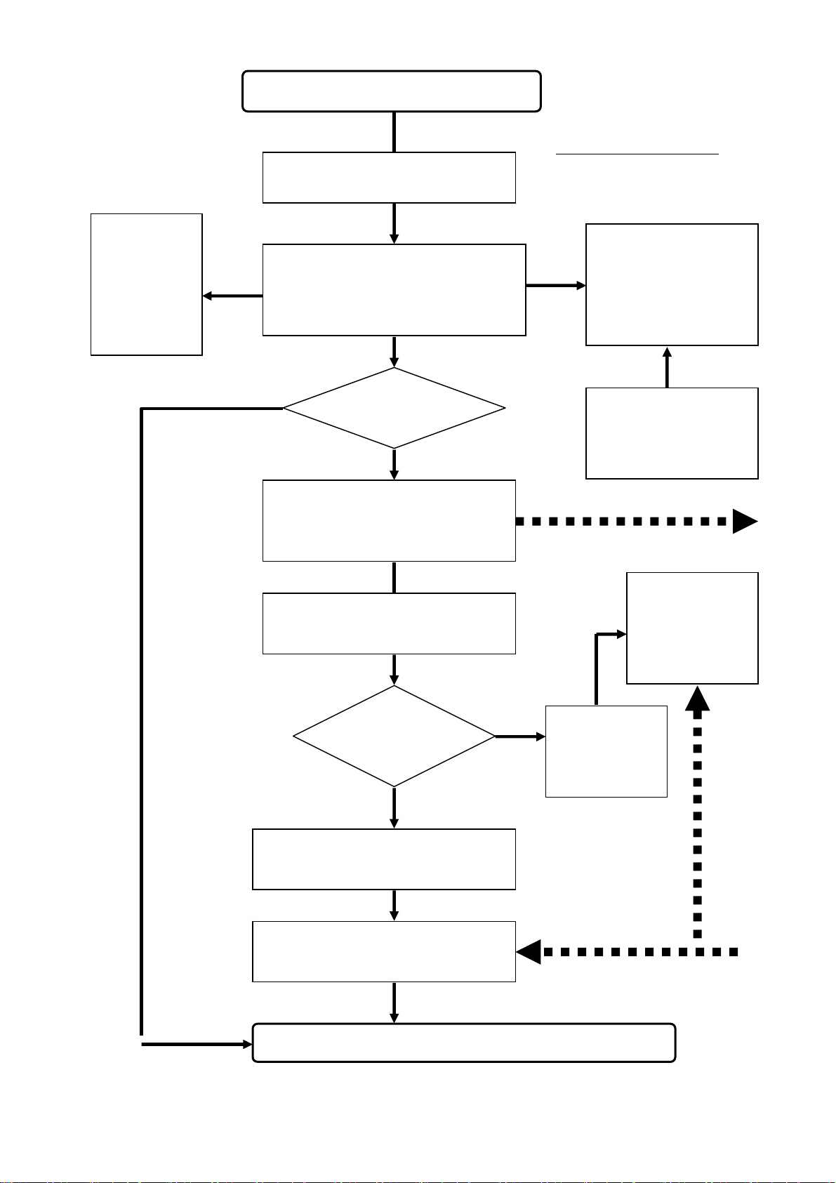
Receive the equipment for
Is warranty period valid?
If not, charge the repair fee.
Physically inspect the equipment.
Check normal operation. Try to
verify the fault.
Fill out a fault report.
Fault
Yes
Send the fault report, faulty
main unit and / or repairable
accessories to Level 2.
cleared?
No
Tell the customer to wait
the estimated maximum
Is the case
urgent?
No
Wait to receive repaired
equipment from level 2.
Physical inspects the
equipment. Check normal
Return the equipment to the customer.
Yes
Flow of Service Level 1
If necessary, replace
any detachable
peripheral parts or
accessories. Discard
consumable
accessories.
Adequate stock of
good replacement
peripheral parts &
accessories
Go to Level 2
Adequate
stock of
good
replacement
Replace the
entire main
unit and
Return From Level
24
KP220 SERVICE MANUAL V1.2
Page 24

TEST EQUIPMENT AND TOOLS FOR SERVICE LEVEL 1
No GSM tester and soldering are required for Service Level 1. The following
equipment and tools are recommended for this level.
1. Fully charged battery :
Use as a power source or a temporary replacement of original battery for
faulty equipment.
2. Workable SIM card :
Used for testing the performance and functions of faulty equipment.
3. Rubber :
Used for cleaning electronic contacts, such as battery terminals, etc.
4. AC Adapter :
Used for testing the charging function of faulty equipment and / or battery.
5. Simple Hands free Kit :
Used for testing the Hands free relevant functions of faulty equipment.
6. USB Cable :
Used for testing the connection between HHP and PC.
25
KP220 SERVICE MANUAL V1.2
Page 25

4-2. SERVICE LEVEL 2
INTRODUCTION TO SERVICE LEVEL 2
The tasks at Service Level 2 will have to :
1. Receive the fault report and faulty equipment from Service Level 1.
2. Verify the faults reported at Level 1 and check the doubtful modular sub-units or
part.
3. Identify the faulty modular sub-unit or part.
4. Disassemble the equipment. Temporarily replace the faulty modular sub-unit or
part with a good one to see if this clears the trouble. Specify the faulty modular
sub-unit or part in the faulty report.
5. Send the fault report and faulty modular sub-unit together to Service Level 3. In
certain cases, replace the faulty modular sub-unit in the equipment with the good
one for quick repair.
6. Receive back the repair report, the repaired modular sub-unit from Service Level 3 and
re-install it in the equipment. Or keep this repaired modular sub-unit for next
replacement, if the faulty modular sub-unit had been replaced with a good one in step 5.
7. Perform the final test with a workable SIM card. Fill out the repair report.
8. Return the equipment to Service Level 1 with the repair report.
26
KP220 SERVICE MANUAL V1.2
Page 26
y
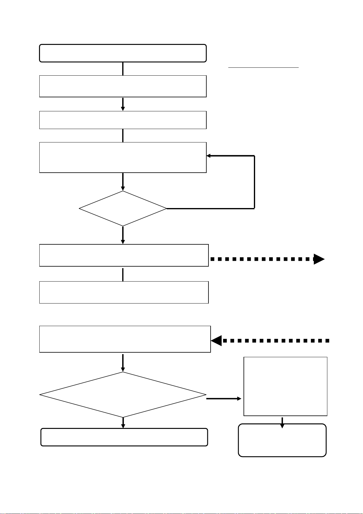
Receive the fault report, faulty equipment.
Verify the faults reported at Service Level 1
Disassemble the equipment.
Temporarily replace the faulty modular sub-unit or
trouble.
Fill out the fault report. Send the fault report
and fault
In certain cases, replace the faulty modular subunit in the equipment with the good one.
Receive back the repair report, the repaired
modular sub-unit from Service Level 3.
Keep as buffer stock for next replacement.
modular sub-unit together to
Had the faulty
equipment been
Fault
cleared?
Yes
lears the part with a good one to see if this c
Yes
-
No
Flow of Service Level 2
Go to Level 3
Return from Level 3
Re-install the
repaired modular
sub-unit in the
No
equipment. Perform
final test and fill out
Return the equipment to
Service Level 1 with the
repair report.
27
Page 27

<< Previous Section
Next Section >>
Main Menu
5
Section 5
Circuit
Description
5-1. LOGIC BLOCK DIAGRAM
5-2. LOGIC
Page 28

Page 29
5-1. LOGIC BLOCK DIAGRAM
Page 30
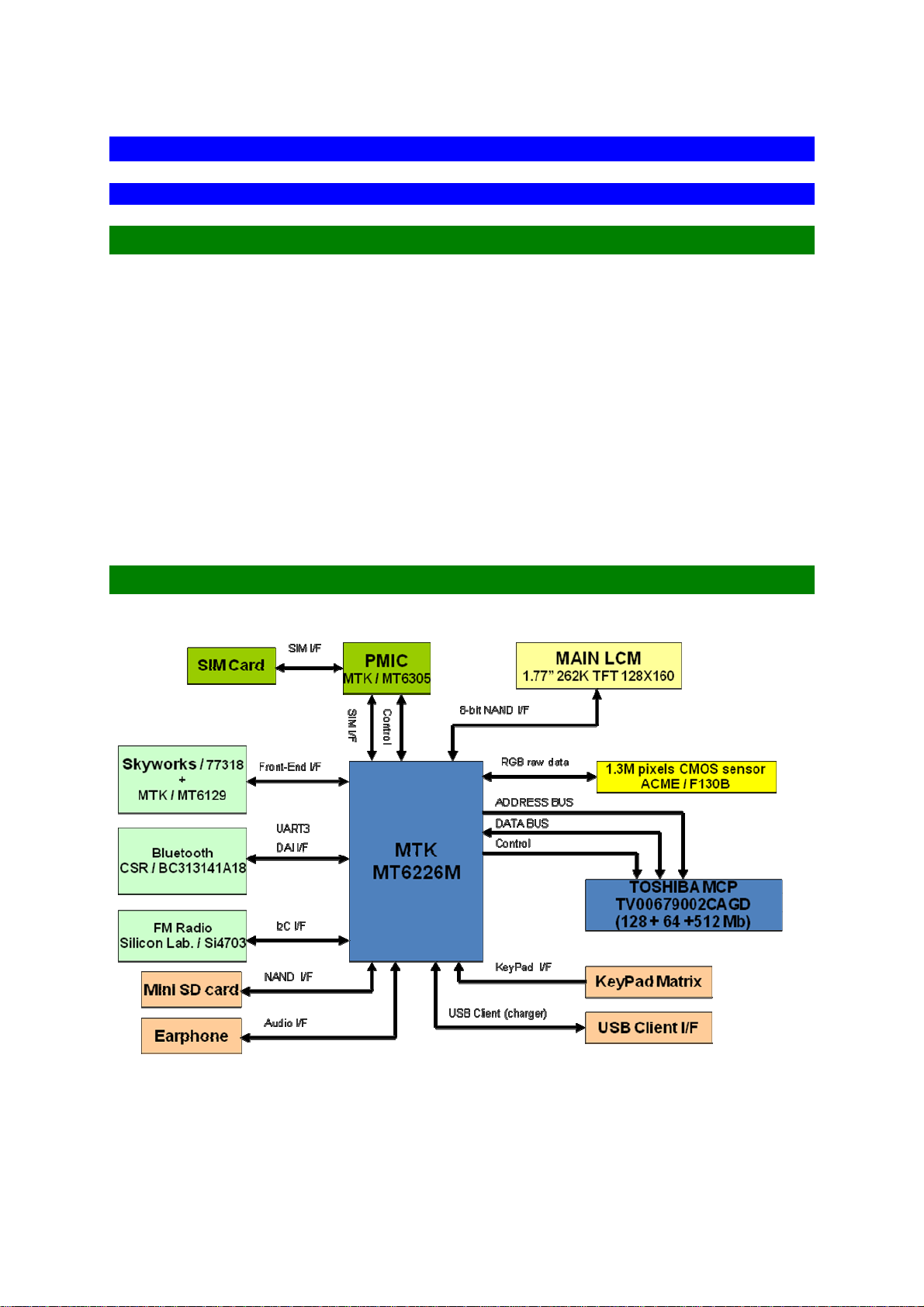
5-2. LOGIC
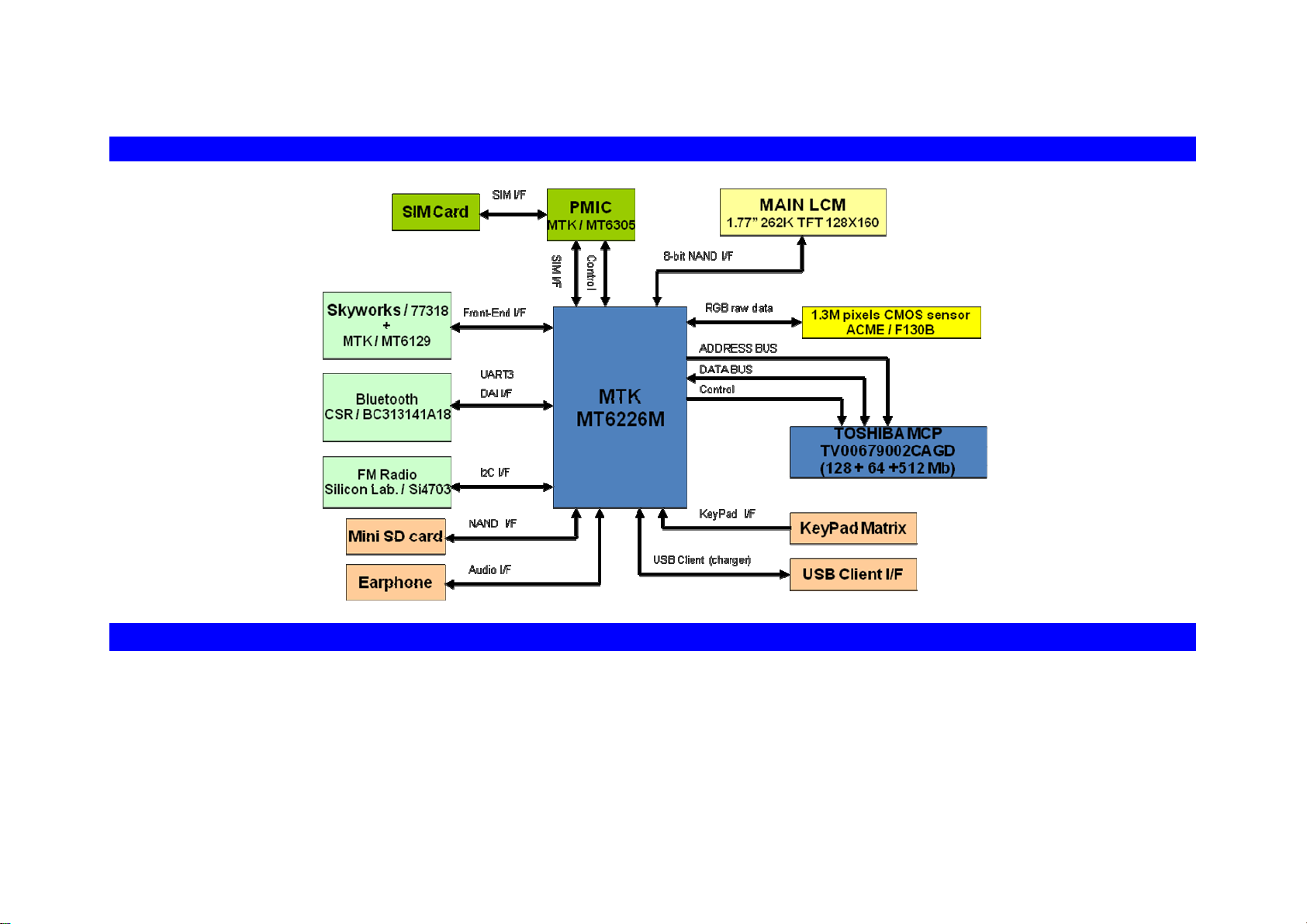
LOGIC AND BASE BAND PORTION
5-2-1. INTRODUCTION
The logic part of 7332 phone is based on Leonardo that is MTK Systems platform.
The circuit comprises the following main functional blocks:
• Memory Subsystem
• Baseband CPU(MTK6226M):
RISC ARM7EJ-STM
• MT6305: PMIC handles all baseband power
• FM Radio IC(SI4703)
• Main LCM (262K TFT)
• Camera (1.3M pixels CMOS sensor)
• Bluetooth(BC313141A18)
• TOSHIBA MCP(128+32+512MB)
• User I/O (KEY,MINI SD CARD,USB Client, SIM card )
Baseband Controller, 52MHz 32bit
5-2-2. SYSTEM BLOCK DIAGRAM
KP220 SERVICE MANUAL V1.2
Page 31

5-2-3. MEMORY SUBSYSTEM
KP220 handset memory;
Memory: (NOR128MB+PSRAM32MB+NAND512MB)
Its detail is as follows.
The consists of 128M-bit NOR Type Flash memory, 32M-bit PSRAM,
NAND512MB in a 107-ball FBGA .
5-2-3.1. Memory
Type and capacity of memories, used for 311-0000-00015 are as follows:
Description Manufacturer Type of memory Capacity
311-0000-00015
TOSHIBA
Flash Memory (NOR)
Flash Memory (NAND) 512Mb
PSRAM
311-0000-00015 is the Stacked Memory comprising of the above four memories.
128Mb
32Mb
5-2-3.2. Memory Interface Description
MT6226 incorporates a powerful and flexible memory controller, External Memory Interface, to
connect with a variety of memory components. This controller provides one generic access scheme
for FLASH Memory, SRAM and PSRAM. Up to 8 memory banks can be supported
simultaneously, BANK0 - BANK7, with a maximum size of 64MB each. Since most of the
FLASH Memory, SRAM and PSRAM have similar AC requirements, a generic configuration
scheme to interface them is desired. This way, the software program can treat different
components by simply specifying certain predefined parameters. All these parameters are based on
cycle time of system clock.
The interface definition based on such scheme is listed in following table. Note that, this interface
always operates data in Little Endean format for all types of accesses
KP220 SERVICE MANUAL V1.2
Page 32

5-2-4. MTK6226 BASE BAND CHIP
Details the block diagram of MT6226. Based on a dual-processor architecture, MT6226 integrates
both an
ARM7EJ-S core and a digital signal processor core. ARM7EJ-S is the main processor that is
responsible for running
high-level GSM/GPRS protocol software as well as multi-media applications. The digital
signal processor handles the low-level MODEM as well as advanced audio functions.
Except for some mixed-signal circuitries, the other building blocks in MT6226 are
connected to either the microcontroller or the digital signal processor.
Specifically, MT6226 consists of the following subsystems:
1.
Microcontroller Unit (MCU) Subsystem - includes an ARM7EJ-S RISC processor and its
accompanying memory management and interrupt handling logics.
2.
Digital Signal Processor (DSP) Subsystem - includes a DSP and its accompanying memory,
memory controller, and interrupt controller.
3.
MCU/DSP Interface - where the MCU and the DSP exchange hardware and software
information.
4.
Microcontroller Peripherals - includes all user interface modules and RF control interface
modules.
5.
Microcontroller Coprocessors - runs computing-intensive processes in place of Microcontroller.
6.
DSP Peripherals - hardware accelerators for GSM/GPRS channel codec.
7.
Multi-media Subsystem - integrates several advanced accelerators to support multi-media
applications.
8.
Vo i ce Front End - the data path for converting analog speech from and to digital speech.
9.
Audio Front End - the data path for converting stereo audio from stereo audio source
10.
Baseband Front End - the data path for converting digital signal from and to analog signal of
RF modules.
11.
Timing Generator - generates the control signals related to the TDMA frame timing.
12.
Power, Reset and Clock subsystem - manages the power, reset, and clock distribution
inside MT6226. Details of the individual subsystems and blocks are described in
following Chapters.
KP220 SERVICE MANUAL V1.2
Page 33

MTK 6226 Interface
KP220 SERVICE MANUAL V1.2
Page 34

5-2-5.PMU IC MT 6305
The MT6305 is a power management system chip optimized for GSM handsets, especially those based on the
MediaTek MT620x system solution. It contains seven Low Drop Out Regulators (LDO), one to power each of the
critical GSM sub-blocks. Sophisticated controls are available for power-up during battery charging, keypad
interface, and RTC alarm. The MT6305 is optimized for maximum battery life, featuring a ground current of only
107μA and 187μA when the phone is in standby and operation respectively.
KP220 SERVICE MANUAL V1.2
Page 35

PMU data
IC sheet
PIN
1
2
3,29
4
5
6
7
8
9
10
11
12
13
14
15
16
17,21,46
18
19
20
22
23
24
25
26
27
28
30
31
32
33
34
35
36
37,40
38
39
41
42
43
44
45
47
48
NAME
CHRIN
Charger Input Voltage
GATEDRV
ISENSE
CHRCNTL
CHRDET
B ATSNS Battery Input Voltage Sense
SIMIO
SIMRST
SIMCLK
S IMVCC SIM Enable
SIMSEL
DGND
RSTCAP
/RESET
VTCXO
AVBAT
AGND
SRCLKEN
PWRKEY
PWRBB
VIBRATOREN Vibrator Driver Enable, Internal Pull Low to DGND
ALERTEREN Alerter Driver Enable, Internal Pull Low to DGND
LEDEN
PGND
VIBRATOR
ALERTER
BATUSE
BATDET
VASEL
VMSEL
VCORE
NC
VSIM
SIO
SRST
SCLK
VM
VBAT
VIO
VRTC
VA
VREF
LED
VBAT
Gate Drive Output
Charger Current Sense Input
Microprocessor Control Input Signal for Gate Drive, Internal Pull Low to DGND
Charger Detect Output
SIM Supply
Non-Level-Shifted Bidirectional Data I/O
Non-Level-Shifted SIM Reset Input, Internal Pull High to VIO
Non-Level-Shifted SIM Clock Input
High for Vsim=3.0V, Low for Vsim=1.8V
Level-Shifted SIM Bidirectional Data Input/Output
Level-Shifted SIM Reset Output
Level-Shifted SIM Clock Output
Digital Ground
Memory Supply
Battery Input Voltage
Digital IO Supply
Real Time Clock Supply
Reset Delay Time Capacitance
System Reset, Low Active
TCXO Supply
Battery Input Voltage for Analog Block Circuits
Analog Supply
Analog Ground
Reference Voltage Output
VTCXO and VA Enable
Power on/off Key, Internal Pull High to VBAT
Power on/off Signal from Microprocessor
LED Driver Enable, Internal Pull Low to DGND
Power Ground
Vibrator Driver Input
Alerter Driver Input
LED Driver Input
Battery Type Selection, High for NiMH, Low for Li-ion, Internal Pull Low to DGND
Battery Detect Input, Low for Battery Connected, Internal Pull High for Battery Disconnected
High for VA enabled with VTCXO, Low for VA enabled with VD, Internal Pull Low to DGND
High for Vm=2.8 V, Low for Vm=1.8V, Internal Pull High to VIO
Battery Input Voltage
Digital Core Supply
FUNCTIO
N
KP220 SERVICE MANUAL V1.2
Page 36

5-2-5.1. Voice Band Interface
The audio front-end essentially consists of voice and audio data paths. Figure 1 shows the block
diagram of the audio front-end. The entire voice band data paths comply with the GSM 03.50
specification. In addition, Mono hands-free audio or external FM radio playback path are provided.
The audio stereo audio path facilitates audio quality playback, external FM radio, and voice
playback through headset.
Figure 2 shows the digital circuits block diagram of the audio front-end. The APB register block is
an APB peripheral that stores settings from the MCU. The DSP audio port block interfaces with the
DSP for control and data communications.
The digital filter block performs filter operations for voice band and audio band signal processing.
The Digital Audio Interface (DAI) block communicates with the System Simulator for FTA or
external Bluetooth modules.
Figure 1 Block diagram of audio front-end
KP220 SERVICE MANUAL V1.2
Page 37

2. Figure 2 Block Diagram of Digital Circuits of the Audio Front-End
Figure 2
5-2-5.2 Monitor ADC
The following is 7332 ADC in use.
External ADC name Purpose in 7332
ADC0_1- Detect Battery Voltage and Current
ADC0_1+ Detect Battery Voltage and Current
ADC2_TBAT Detect Battery tempter
ADC3_VCHG Detect Charging voltage
ADC5_USB Detect USB device
ADC6_ASS_ID Detect hand free
KP220 SERVICE MANUAL V1.2
Page 38

Circuit Diagram
5-2-6. KEY SWITCHES
KP220 SERVICE MANUAL V1.2
Page 39

KP220 SERVICE MANUAL V1.2
Page 40

Circuit Diagram
5-2-7. VIBRATOR
5-2-8. KEY BACKLIGHT LED
There are eight LEDs used for key backlighting. The LED driver of 6305 controls
these LEDs.
Circuit Diagram
KP220 SERVICE MANUAL V1.2
Page 41

5-2-9 BATTERY CHARGING
Battery management, which controls charge and discharge of the battery is
the most important function for safety. 7338 SW performs charging algorithm. To
regulator the power PMOS for set the charging current.
KP220 CHARGING CIRCUIT AND ALGORITHM
charging Circuit and Algorithm
7338 Charging circuit:
The schematic below shows the external charging components used in the Arima
7338 project. All ports are directly connected to the corresponding pins of PMU IC
(6305). VCHG is the V charger supply rail coming directly from the wall-plug constant
voltage charger via the system connector, and VBAT is the Battery Voltage rail,
connected directly to the battery pack terminal connector. The system uses a solid
ground plane, and both the Battery Pack terminal and the wall-plug charger return
paths are connected directly to ground.
KP220 SERVICE MANUAL V1.2
Page 42

Charger Sub-system
The MT6305 battery charger can be used
with Li-ion and NiMH batteries. BATUSE
pin can set MT6305 to fit the battery type.
When BATUSE is set low, Li-ion battery is
used. When BATUSE is set high, then
NiMH battery is used. MT6305 charges
the battery in three phases: pre-charging,
constant current mode charging, and
constant voltage mode charging. Figure 2
shows the flow chart of charger behavior.
The circuitry of MT6305 combines with a
PMOS transistor, diode and current-sense
resistor externally to form a simple and
low cost linear charger shown in Figure 3.
MT6305 is available pulsed top-off
charging algorithm by the CHRCNTL pin
control from baseband chipset.
Charge Detection
The MT6305 charger block has a
detection circuit that determinates if an
adapter has been applied to the CHRIN
pin. If the adapter voltage exceeds the
battery voltage by 3.75%, the CHRDET
output will go high. If the adapter is then
removed and the voltage at the CHRIN
pin drops to only 2.5% above the VBAT
pin, CHRDET goes low.
Pre-Charging mode
When the battery voltage is below the
UVLO threshold, the charge current is in
the pre-charging mode. There are two
steps in this mode. While the battery
voltage is deeply discharged below 2V, a
10mA trickle current of MT6305 charges
the battery internally. When the battery
voltage exceeds 2V, the pre-charge
current is enabled, which allows 10mV
(typically) across the external current
sense resistor. This pre-charge current
can be calculated:
KP220 SERVICE MANUAL V1.2
Page 43

Constant Current Charging Mode
Once the battery voltage has exceeded the UVLO threshold the charger will switch to the constant
current charging mode. The MT6305 allows 160mV (typically) across the external current sense resistor.
This constant current can be calculated.
If the voltage of Li-ion battery is below 4.2V (5.1V for NiMH battery), the battery will be in the
constant current charging mode.
Constant Voltage Charging Mode
This mode is only applied to Li-ion battery charging. If the battery has reached the final charge
voltage, a constant voltage is applied to the battery and keeps it at 4.2V. The charge termination is
determined by the baseband chip internally, which will pull the CHRCNTL low to stop the charger. Once
the battery voltage exceeds 4.3V of Li-ion battery (5.1V of NiMH battery), a hardware over voltage
protection (OV) should be activated and turn off the charger block of MT6305.
Pulsed Charging Algorithm
MT6305 is available to pulsed top-off charging algorithm by the CHRCNTL pin. The control signal is
from baseband chipset to limit the charging duty cycle. This charging algorithm combines the efficiency
of switch-mode chargers with the simplicity and low cost of linear chargers.
Battery Voltage Monitor
As the Table 2 shown, the relations of battery voltage and charger control signals are listed. When
Vbat < 3.2V, an UVLO signal is active low. When Vbat >= 4.3, an OV signal is active and terminates
charging. The disconnection of battery could be detected by BATDET pin. BATDET is pulled high
internally when battery disconnected and terminates charging immediately.
KP220 SERVICE MANUAL V1.2
50
Page 44

5-2-10. REAL-TIME CLOCK (RTC)
RTC is the feature to count “second”.
MTK6226M’s clock generation on 32.768kHz is made by OSC(X401 in 7338),
connecting to OSC32K_IN/ OSC32K_OUT and supply the clock to 6305.
KP220 SERVICE MANUAL V1.2
Page 45

TThe real-time clock (RTC) is driven by a 32.768 kHz clock from a crystal oscillator.
he input clock is di cond period. In
ddition, it can gene wing are basic
function of RTC:
- ime information (seconds/minutes/hours) coded in T
-Calendar information (Day/Month/
ear 2099.
y
larm function with interrupts generation bases on a periodical
-A
econd/minute/hour/day) or a precise time event in the century (second accuracy).
(s
0s time range correction
-3
2khz oscillator frequency gauging.
-3
he RTC module of 7338 is supplied by 3V Backup Battery made by Sanyo.
T
he target of running time of the backup battery (fully charged) is longer than two
T
ours after the main battery is removed.
h
vided by 32.768 to generate a clock with a 1 se
rate interrupts at a programmed time. The folloa
BCD
Year/Day of the week) directly in BCD code up to
51
KP220 SERVICE MANUAL V1.2
Page 46

5-2-11. EXTERNAL INTERFACE
The pin arrangement of system I/O is shown below.
52
KP220 SERVICE MANUAL V1.2
Page 47

5-2-12. SIM INTERFACE
he SIM int
T
module smart card. With the appropriate software and level conversion by MT6305,
the interface is compliant with GSM 11.11 a
SIMVCC
This output connects to contact C306 (VCC) of the SIM conne
supply power to the SIM card and is supplied directly from MT6305.
It is controlled by MTK6226M , and enable the power and 3V operation
respectively. Note that while SIMPWR is low, the software sets SIMRST, SIMCLK
and SIMDATA signals low.
SIMRST
This output connects to contact V502 (RST) of the SIM connector. It is set directly
by the CPU writing to the SIM control register.
SIMCLK
This output connects to contact V501 (CLK) of the SIM connector. The clock may
be set high or low, or a choice of 13/4 MHz or 13/12 MHz clock frequencies may
be selected, by writing to the SIM control register. In order to save power, the
clock should be stopped when not required, if the SIM allows it.
SIMDATA
This is a bi-directional, open drain signal, connected to contact V504 (I/O) of the
SIM connector. Control of the data signal is done in the SIM interface section of
MTK6226M, although the output can be disabled by writing to the SIM control
register. Being open-drain with an external pull-up, the output floats high when
not being driven low by either Trident-HP or the SIM card.
All the above control signals maintain their state when MTK6226M is powered down.
This allows the SIM to remain powered during soft-OFF. SIMPWR should be
switched OFF when handset ‘hard-OFF’ mode is selected.
erface module within MTK6226M allows access to the subscriber identity
nd GSM 11.12.
The electrical interface consists of five signals:
ctor. It is used to
53
KP220 SERVICE MANUAL V1.2
Page 48

5-2-13. SIGNAL CONTROL PATH FOR BACKLIGHT LED,
CAMERA FLASH LED AND INDICATOR LED
5-2-13.1 Backlight LED Control
The LCD backlight is controlled by the PWL signal from the MTK6226M. The
backlight is turned on when PWM1_LCM_EN is high. The LCD backlight a 5V power
supply. The RT9396 DC/DC converter (U801) generates the signal for
LED1,LED2 ,LED3 Detailed circuit diagram is as shown below.
KP220 SERVICE MANUAL V1.2
Page 49

5-2-13.2 Camera Control
Overview of voltage supply for Camera
RT9182 provides power supply for Camera shown below.
KP220 SERVICE MANUAL V1.2
Page 50

5-2-14. DISPLAY SYSTEM
2-14.1 TFT LCD Module
5-
The IM177BBNBA model is a Color TFT LCD supplied by LG .
This Module has a 1.77 inch diagonally measured active display area with
128(RGB)X160 resolution
Each pixel is divided into Red, Green and Blue sub-pixels and dots which are
arranged in vertical stripes.
LCD color is determined with 262K Colors signal for each pixel.
The IM177BBNBA has been designed to apply the interface method that
enables low power, high speed, and high contrast.
The IM177BBNBA is intended to support applications where thin
thickness, wide viewing angle and low power are critical factors and
graphic displays are important.
Item Main Display Remark
Display Mode
Normally White, Tran missive LCD
Driving Method TFT Active Matrix
Input Signals 8bit CPU I/F Parallel
Outside Dimensions 33.9mm(W) x 46.4mm(H) x 2.1mm(D) (Typ.)
Active Area 28.032mm(W) X 35.04mm(H)
Number of Pixels
Pixel Pitch 0.219mm(H) X 0.219mm(W) Note 1)
Pixel Arrangement
128×RGB×160 Pixels
RGB Vertical stripes
Note 1)
Note 1)
56
KP220 SERVICE MANUAL V1.2
Page 51

5-2-14.2 LCD interface
KP220 SERVICE MANUAL V1.2
57
Page 52

5-2-15.1 Camera Module
5-2-15. CAMERA
5-2-15.2 Specifications
KP220 SERVICE MANUAL V1.2
Page 53

5-2-16. AUDIO SUBSYSTEM
5-2-16.1 Outline
The audio system is composed of MTK6226M, PMU IC (MT6305). The attached
device is MIC, Receiver, Speaker.
5-2-16.2. Audio Control
Speaker interface
Use U702 to amplify voice and voice signal from MP3_OUTL
Receiver and Microphone
The receiver is a 32Ω dynamic type and is driven directly from MT6305.
The Microphone is also directly connected to MT6305 MICIP0 and MICIN0.
NEC Confidential & Proprietary
Page 54

Hands Free Interface
NEC Confidential & Proprietary
Page 55

5-2-17 FM interface
MT6226 integrates a mixed-signal Baseband front-end in order to provide a wellorganized radio interface with flexibility for efficient customization. It contains gain
and offset calibration mechanisms, and filters with programmable coefficients for
comprehensive compatibility control on RF modules. This approach also allows the
usage of a high resolution D/A Converter for controlling VCXO or crystal, thus
reducing the need for expensive TCVCXO. MT6226 achieves great MODEM
in
performance by utilizing 14-bit high resolution A/D
Furthermore,
driving
strength of some BPI outputs is designed to be configurable.
to
reduce the need for extra external current-driving component, the
Converter
the RF downlink path.
NEC Confidential & Proprietary
Page 56

5-2-18 Bluetooth interface
BuleCore3-ROM CSP is signal chip radio and baseband chip for Bluetooth wireless
technology 2.4G Hz system .it is implemented in 0.18um CMOS technology.
The 4Mbit ROM is metal programmable ,which enables an eight week turn-around
from approval of firm are to production samples.
NEC Confidential & Proprietary
Page 57

5-2-19 RF Sub-systems
MT6129 is a highly integrated RF transceiver IC for multi-band Global Systems for
obile communication (GSM) and General Packet Radio Service (GPRS) cellular M
system applications. The MT6129 includes four LNAs, two RF quadrature mixers, an
integrated channel filter, programmable gain am
the
receiver, a precision IQ modulator with offset PLL for the transmitter, two internal
TX VCOs, a VCXO, on-chip regulators, and a fully programmable sigma-delta
fractional-N synthesizer with an on-chip RF VCO. The MT6129 also includes contr
circuits to enable different operating modes. The device is housed in a 56-pin Q
SMD package with a down set paddle for additional grounding.
plifiers (PGA), an IQ demodulator for
ol
FN
NEC Confidential & Proprietary
Page 58

5-2-19.1 Receiver
The receiver section of MT6129 includes Quad-band low noise amplifiers (LNAs),
RF
quadrature mixers, an on-chip channel filter, Programmable Gain Amplifiers
(PGAs), quadrature second mixers, and a final low-pass filter. The very low-IF
MT6129 uses image-rejection mixers and filters to eliminate int
accurate RF quadrature signal generation and mixer matching techniques, the image
rejection of the MT6129 can reach 35 dB for all bands. The fully integrated channel
filters rejects interference, blocking signals, and images without any external
components. Compared to a
arc
hitecture improves the blocking rejection, AM suppression, as well as the
adjacent channel interference performance. Moreover, the very low-IF architectu
eliminates the need for complicated DC offset calibration that is necessary in a DCR
architecture. In addition, the common-mode balance requirement of the SAW filter
put is relaxed. The MT6129 provides the analog IQ baseband outpin
xtra frequency conversion components.
e
The MT6129 includes four differential LNAs for GSM 850 (869 MHz – 893 MHz
E-GSM 900 (925 MHz-960 MHz), DCS 1800 (1805 MHz-1880 MHz) and PCS 1900
(1930 MHz –1990 MHz). The differential inputs are matched to 200 _ SAW filters
using LC networks. The gain of the LNAs can be controlled either high or low for an
additional 35 dB dynamic range control. Following the LNAs are the image-rejection
quadrature RF mixers that down-convert the RF signal to the IF frequency. No
external components are needed at the output of the RF mixers.
The IF signal is then filtered and amplified through an image-rejection filter and a
PGA. The multi-stage PGA is implemented between filtering stages to control the
gain of the receiver. With 2 dB gain steps, a 78 dB dynamic range of the PGA
ensures a proper signal level for demodulation. The quadrature 2nd mixers are
provided on-chip to down convert IF signal to baseband in an analog differential IQ
format.
direct conversion receiver (DCR), MT6129’s very low-IF
erference. With
re
ut without any
),
5-2-19.2 Transmitter
The MT6129 transmitter section consists of two on-chip TX VCOs, buffer
amplifiers, a down-converting mixer, a quadrature modulator, an analog phase
detector (PD) and a digital phase frequency detector (PFD), each with a charge
pump output and on chip loop filter. The dividers and loop filters are used to achieve
the desired IF frequency from the down-conversion mixer and quadrature modulator.
For a given transmission channel, the transmitter will select one of the two different
TX reference dividing numbers. These built-in components, along with an internal
voltage controlled oscillator (TX VCO) and a loop filter, implement a translation loop
modulator. The TX VCO output is fed to the power amplifier (PA). A control loop,
implemented externally, is used to control the PA’s output power level.
NEC Confidential & Proprietary
Page 59

5-2-Tw1
he TX ypically 9 dB th +/- 2.5dB variation in E-GSM900/
T VCO output power is t
SM8 utput power
CS19 me temperature conditions. Inside the chip, the VCO
P
ifferen re fed into the output buffer, the OPLL input feedback
d
uffer, and the calibration circuit. The off chip signal is transformed into a single
b
nded output which needs impedance matching to 50_to drive the power amplifier.
e
ike RF VCO, the oscillation bandwidth is partitioned into 128 (or 64) sub-bands for
L
CS/ PCS (for E-GSM900/ GSM850) TX VCO to cover the process and temperature
D
ariation. Calibration process begins after a period of programmable time when the
v
n chip TX VCO regulator is turned on. Total calibration time needs about 60us
o
aximally and the frequency error after calibration is within +/-5 MHz. For Vtune =
m
.2 V, the variation of kvco is about 14% and 40% for GSM and DCS/PCS TX VCO,
1
espectively, across the desired fre
r quency range.
9.3 TX VCO
o power VCOs are integrated w P
50 bands and +8 dB
00 bands over extre
tial output signals a
m o
ith O LL to form a complete transmitter circuit.
s
m wi
with +/- 2dB variation in DCS1800/ G
5-2-19.4 Frequency Synthesizer
The MT6129 includes a integrated RF VCO to
generate RX and TX local oscillator frequencies. The PLL locks the RF VCO to a
precision reference frequen the inherent spur
aused by fractional-N syn modulator with
ithering function is used to generate the presale divider number N. The presale is
d
ased on a multi-modulus architecture with programmable divider numbers ranging
b
om 64 to 127. A conventional digital-type PFD with a charge pump is used for
fr
hase comparison in the PLL. By changing the output current of the charge pump,
p
e phase detector gain can be programmed from75/_ _A/rad to 600/_ _A/rad.
th
To reduce the acquisition time or to enable
services such as GP
system are implemente
loop. After the calibr
cilitate fast locking. Once the acquisition is done, the PLL reverts back to the
fa
ormal operation mode.
n
RS, a digital loop (calibration loop) along with a fast-acquisition
et tthe RF VCO is pre-s
ation, a fast-acquisition system is utilized for a period of time to
frequency synthesizer with a fully
cy at 26 MHz. In order to reduce
thesizers, a 3rd-order sigma-deltac
fast settling time for multi-slot data
d in the synthesizer. Once the synthesizer is programmed,
o the vicinity of the desired frequency by a digital calibration
NEC Confidential & Proprietary
Page 60

5-21-19.5 Volta
Voltage Control Crystal Oscillator (VCXO) consists of an amplifier, a buffer, and a
programmable
reference freq
eries resonance with a standard 26 MHz crystal. The crystal is connected from the
s
put pin XTAL of amplifier to ground through a series load capacitance. The buffer
in
rovides a typical 600mVpp voltage swing at either 13 MHz or 26 MHz. It is designed
p
to drive a tuned load to improve harmonic contents and reduce the oscillator current
consumption. The capacitor array, from 0.0625 pF to 4 pF in steps of 0.0625 pF, is
used to shunt the series load capacitor for coarse tuning and remove any fixed
offsets due to crystal manufacturing variations. An internal varactor that provides fine
tuning combines with the capacitor array. As an alternative, the reference frequency
can be provided by an external 26 MHz VCTCXO module.
When pin VCXOCXR is tied to the VCCVCXO supply, the XTAL pin will accept
an external signal. Furthermore, the VCXO control pin can be tied to VCCVCXO to
prevent the current leakage during the sleep mode operation.
capacitor array. The VCXO provides the MT6129 with a selectable
uency of either 13 MHz or 26 MHz. The amplifier is designed to be in
ge Control Crystal Oscillator
5-2-19.6 Regulator
The MT612X internal regulators provide low noise, stable, temperature and
independent supply voltages to critical blocks in the transceiver. An internal Pchannel MOSFET pass transistor is used to achieve a low dropout (LDO) voltage of
less than 150 mV in all regulators.
69
NEC Confidential & Proprietary
Page 61

<< Previous Section
Next Section >>
Main Menu
SECTION 6
6
6-1. Structure
6-2. Accessories
6-3. Soldering
Servicing
70
NEC Confidential & Proprietary
Page 62

6-1. STRUCTURE
1. KP220
Front View Back View
72
NEC Confidential & Proprietary
Page 63

MAIN BOARD ASSEMBLY
he lower board consists of the following cir
T cuits:-
1.Tri band GPRS GSM Transceiver and logi
nection socket 2.SIM con
3.System
4.battery term
6.Embedded tri
7.Vibrator conn
9.Camera con
10.Receiver connection terminal
11.Speaker connection terminal
12.SD Card connection terminal
13.LED, camera control and LCD driver circuit
I/O connector with charge capability
inals
jack
ree5.Hands f
band antenna connection terminal
ection terminal
connection terminal
8.Microphone
nection terminal
c Unit
NEC Confidential & Proprietary
Page 64

FRONT COVER
The Front cover contains following m
.Receiver
1
2.Keypad
ain parts :-
2. keypad
1.Receiver
NEC Confidential & Proprietary
Page 65

REAR COVER
The Rear cover contains following main parts :-
1. Speaker
2. Vibrator
3. Microphone
4. Antenna
5. Charger cover
6. SD card cover
7. Volume key
8. Camera key
Charger cover
vibrator
microphone
Antenna
SD Card cover
speaker
Volume key
Camera key
75
KP220 SERVICE MANUAL V1.2
Page 66

6-2. ACCESSORIES
BATTERY
AC ADAPTER
KP220 SERVICE MANUAL V1.2
Page 67

HANDSFREE & USB CABLE
Cable
KP220 SERVICE MANUAL V1.2
Page 68

6 -3.SOLDERING
SOLDERING PARTS LOCATION
SOLDERING REPAIRED PARTS AT SERVICE LEVEL 2 ARE SHOWN AS BELOW.
Bluetooth
BC313141A18
RTC
32.768KHz
antenna switch
ESHS-C085TK
PA
SKY77318
PMIC
MT6305
Cr
ystal
26 MHZ
MCP Memory
TV00579002EAGD
LDO
LP3995
Baseband Controller
Status
LED
Key Board
Connector
FM Receiver
Si4703
Receiver
Contact
MT6226
LCM
Hot Bar
KP220 SERVICE MANUAL V1.2
Page 69

A
A
Micro SD
Slot
Microphone
Contact
Vibrator
Contact
Battery
Contact
LDO
RT918 2
SIM Card
Connector
ntenna
Pogo Pin
RF Switch Connector
MM8430
KP220 SERVICE MANUAL V1.2
Camera Modu
Socket
le
udio Amplifier
LM4671
Speaker
Contact
Mini USB
Connector
Page 70

DC
-DC
MO
P Ch
SFE
Si58
annel
T+Sch
53DC
ottky
TV
PES
TVS
ESD
S ARR
D5V0L
CONVER
ARRAY
5V0L5UY P
LDO
298LP 5
AY
5UY
RT9
363
T
TCXO
26MHz
GS
M/G
PRS
Tra
nscei
ver
S
AW
Fil
5EB
ter
-9
42M50FA
R-F
Backup Batt
XH414H IV01E
KP220 SERVICE MANUAL V1.2
ery
S
FAR-AWF6E
SAW Filter
Filt
B-1erG 8425
B-1FAR- GF6E 9600
95
Page 71

<< Previous Section
Next Section >>
Main Menu
7
Repairing
7-1. Testing
7-2. Troubleshooting
Section 7
97
KP220 SERVICE MANUAL V1.2
Page 72

7-1. TESTING
OVERVIEW
1. Product overview and frequency assignment
TX E-GSM 880MHz to 915MHz (deltaF=2
RX E-GSM 925MHz to 960MHz (deltaF=200KHz)
Radio Frequency Band
ARFCN
RF Loc
T requency X IF F
Access form 8 channel multiple TDMA
Multiple 8 channel / carrier ( E-GSM/DCS1800/PCS1900)
Modulation 270.8333Kbit/s GMSK
Peak output power
Nominal supply
voltage
TX peak current 2500mA max.
GPRS Class Class10 (max 1UL/4DL) Operation class B
GPRS Coding scheme CS1/CS2/CS3/CS4
al Synthesizer
TX DCS1800 1710MHz to 1785MHz
RX DCS1800 1805MHz to 1880MHz
TX PCS1900 1850MHz to 1910MHz
RX PCS1900 1930MHz to 1990MHz
E-GSM Ful(n) = 890 + 0.2 x n at ( 0 <= n <= 124 )
Ful(n) = 880 + 0.2 x (n-1024) at ( 975 <= n <= 1023)
Fdl(n) = Ful(n) + 45
DCS1800 Ful(n) = 1710.2 + 0.2 x (n-512) at ( 512 <= n <= 885 )
Fdl(n) = Ful(n) + 95
PCS
1900 Ful(n) = 1850.2 + 0.2 x (n-512) at ( 512 <= n <= 810 )
Fdl(n) = Ful(n) + 80
E-GSM 1279~1314 MHz
DCS1800 1327~1402 MHz
PCS1900 1423~1483 MHz
E-GSM 798 MHz (Typ) (880-895 MHz, 900-915 MHz)
790 MHz (Typ) (895-900 MHz)
DCS1800 766 MHz (Typ)
PCS1900 854 MHz (Typ)
E-GSM 2W(33dBm) Class4 MTS
DCS1800 1W(30dBm) Class1 MTS
PCS1900 1W(30dBm) Class1 MTS
+3.8V
00KHz)
2. Channel selection conditions
Verify that there is no interference from other radio devices or neighboring
easurement systems in the frequencies to be used for the test. If there is
m
terference, select the test channels within the range of the following channels.
in
specially in case of bit error tests, make sure that there is no influence from outside
E
efore the test. If necessary, use a shielded box or take other channel measures.
b
E-GSM DCS1800 PCS1900
Lch
Mch
Hch
975ch to 980ch 513ch to 523ch 512ch to 522ch
60ch to 65ch 690ch to 710ch 657ch to 667ch
120ch to 124ch 874ch to 884ch 800ch to 810ch
KP220 SERVICE MANUAL V1.2
98
Page 73

3. Product Specification
Based on GSM 11.10-1 / 3G TS 51.110
4. Measurement adapter
Dumm
Test S
RF connect
PC-Link cable
y battery
Dummy battery should be used shown as follows:
IM card
In confidence test, general Phase2 (or Phase2+) test SIM should be used.
or and RF cable
RF
connector and RF cable should be used for RF test
PC-link cable (Serial Link Cable) should be used.
99
KP220 SERVICE MANUAL V1.2
Page 74

. Test purpose
1
a) To verify Ap
b) To verify re
c) To v
d) To verif
erify Function Test in the table shown as below
FUNCTION TEST
pearance by visual check
cognition of SIM card
y power down phone
2. Te
3 st Procedure
a. Power on Phone
*#878#
Select item 1 “Servi
st System
1. nit (PSU)+Dummy Battery or Battery
Power Supply U
2. SM Phase 2+ Test SIM Standard 1(3.1))
Test SIM Card (Spec: G
3. (SHF, Stereo)
Sample Hands free Kit
. Te
3.1 Appearance Test
Verify appearance by visual check
3.2 SIM Test
Verify recognition of SIM card
If “Insert SIM” indicated on Display, it is NG.
3.3 Enter Service Mode
3.1.1 No SIM Card installed
b. Press 878 to enter service mode.
3.1.2 SIM Card installed
a. Power on Phone
b. Press to enter service mode.
3.1.3 Software Version Check
ce Info” in Service mode to check software version.
100
KP220 SERVICE MANUAL V1.2
Page 75

3.4 MMI Tests
1. Auto test
2. BT Mode
3. Echo Loop
4. Version
. Resource B
5 IN
6. Keypad
7. Vibrator
8. Loud SPK
9. Ring Tone
10. LED
11. LCD
12. Receiver
13. ADC
14. Ch
15. Hea
16. R
17. MT
18
19. Memory Card
20. Nand Flash
arger
dset
TC
BF
. UART
21. Camera
22. Total call time
23.
FM Radio
101
KP220 SERVICE MANUAL V1.2
Page 76

. Te
1 st purpose
This test is for check RF characteristics.
. Test system
2
1. PC
2. Printer
3. PSU
4. GSM Test Set
5. USB Cable
6. UART Cable
7. Calibration Adapter
8. RF Cable
Measurement setup is shown
Test Instruments
1. PC
2. PRINTER
CONFIDENCE TEST
as follows:
5. USB Cable
6. UART Cable
4. GSM Test Set
E5515B
(HP8960)
Calibration adapter
Lower
Board
8. RF Cable
3. PSU
HPE3631A
102
KP220 SERVICE MANUAL V1.2
Page 77

3. Test Specification
Measurement item and specification is defined as follows:
Test Item
TX Maximum Power
T
X Power
R
MS Phase error
PEAK Phase error
Frequency Error
P
ower Vs Time
R
X Class2 RBER
R
X Level
R
X Quality
31dBm +
29dBm + B @ PL7
27dBm + @ PL8
25dBm +
23dBm +/ L10
21dBm +/
19dBm +
17dBm +
15dBm /- 3dB @ PL14
13dBm +/- 3dB @ P
11dBm +/
9dBm +/ B @ PL17
7dBm +/ B @ PL18
5dBm +/
pass/ ail specification is shown as table 4.1
Specification
E-GSM DCS1800 PCS1900
33dBm +/-2dB 30dBm +/-2dB
/- 3dB @ PL6
/- 3d
/- 3dB
/- 3dB @ PL9
- 3dB @ P
- 3dB @ PL11
/- 3dB @ PL12
/- 3dB @ PL13
+
L15
- 5dB @ PL16
- 5d
- 5d
- 5dB @ PL19
< < 180Hz < 185Hz 90Hz
fail indication. Det
<2.4% @ -10
<5deg
<20deg
3.5dBm (avg 10000bit)
7 +/-4 @
<3 @ -1
28dBm +/- 3dB @ PL1
26dBm +/- 3dB @ PL2
24dBm +/- 3dB @ PL3
22dBm +/- 3dB @ PL4
20dBm +/- 3dB @ PL5
18dBm +/- 3dB @ PL6
16dBm +/- 3dB @ PL7
14dBm +/- 3dB @ PL8
12dBm +/- 4dB @ PL9
10dBm +/- 4dB @ PL10
8dBm +/- 4d
6dBm +/- 4d
4dBm +/- 4dB @ PL13
2dBm +/- 5dB @ PL14
0dBm +/- 5dB @ PL15
-103.5dBm
03.5dBm
B @ PL11
B @ PL12
103
KP220 SERVICE MANUAL V1.2
Page 78

(*)
(**)
wer Vs Time mask specification Po
dB
+ 4
+ 1
- 1
- 6
(**)
- 30
(***)
(147 bits)
(*)
8
탎
10
탎
10
Time mask for ormal d tion bursts(NB,FB,dB and SB) at GM
탎
n ura SK modulation
7
056/13 (542.8)
10 탎8
탎
탎
10
탎
t
For GSM 900 MS the
For DCS1800 and PCS1900 the
MS : -48 dBc or -48 dBm, whichever is
: -59 dBc or -54 dBm, whichever is
greater, except for th
preceding the active slot, for w
the allowed level is -59
e time slot
hever isor -36 dBm whic
hich
dBc
the greater
higher.
For GSM 900 MS
-4 dBc for powe:
-2 dBc for power level 1
r control level 16;
7;
level co-1 dBc for power
ntrols levels
18 and 19.
For DCS1800 and PCS1900
-4dBc for power contro MS :
-2dBc for power level
-1dBc for power control levels 13,1
l level 11,
12,
4
and 15
For GSM S : -30 dBc or -17 dBm, whichever is the
900 M (***)
higher.
For DCS1800 an 00
d PCS19 MS : -30dBc or -20dBm, whichever is the
higher.
104
KP220 SERVICE MANUAL V1.2
Page 79

4. Test Pr
Test items should be s
of GSM test set, th est shou over to
oce
dure
equential in the table shown as below. Due to
e t ld be started under E-GSM mode and hand
limitation
DCS1800. In PCS1900 mode, the test should be started under PCS1900 mode.
fault se M ws:
De tting of GS test set and PSU is shown as follo
(Internal L (Please measure cable loss on first se
CALL STATUS IDLE
CELL STATUS ACTIVE CELL
OPERATING MODE E-GSM
Expected input level TX Level 5 : 33dBm
Control Base station Broadcast Broadcast ON
Control Base station Channel 20
Control Base station Amplitude -85dBm
Mobile Phone Channel 62 ( could be changed ARFCN Mch )
Mobile Phone TX Level 5
Mobile Phone Timeslot 4
PSU output voltage +3.8V +/- 0.05V
PSU maximum current limit 2500mA
oss) t-up and calibrate
it.)
CALL STATUS IDLE
CELL STATUS ACTIVE CELL
OPERATING MODE PCS1900
Expected input level TX Level 0 : 30dBm
Control Base statio stn Broadca Broadcast ON
Control Base station Channel 512
Control Base station Amplitude -85dBm
Mobile Phone Channel 661 ( could be changed ARFCN Mch )
Mobile Phone TX Level 0
Mobile Phone Timeslot 4
PSU output voltage +3.8V +/- 0.05V
PSU maximum current limit 2800mA
105
KP220 SERVICE MANUAL V1.2
Page 80

Test item MODE Procedure
Start up
E-GSM 1. Set SIM card and dummy battery to HHP
2. Power on HHP
3. Wait to indicate “GSM Test Net 001”
Call setup
X Power
T
RMS Phase error
PEAK Phase error
Frequency Error
Power Vs Time
RX Class2 RBER
RX Level
RX Quality
Hand over
Close down
*1 Refer to 1.Overview Channel selection condition
E-GSM 1. Input the PTE comma “StartCall” nd
2. “Receivecall”. Input the PTE command
3. Wait to indicate “Active” to establish call
E-GSM
DCS
1800 Set PL to 5(E-GSM)
E-GSM
DCS1800
E-GSM
DCS1800
E-GSM
DCS1800
E-GSM
DCS1800
E-GSM
DCS1800
E-GSM
DCS1800
E-GSM 1. Same sett RX RBER ing and procedure as
E-GSM to
DCS1800
( Test is repeated under DCS1800 band )
DCS1800 1. Push “END Call” of GSM tester
1. ARFCN is assign to Mch ( and Lch/Hch )
2. or 0(DCS1800)
3. Wait to establish hand over
4. power Measure output
1. Hch ) ARFCN is assigned to Mch ( or Lch/
2. Set PL to 5(E-GSM) or 0(DCS1800)
3. Wait to establish hand over
4. Change mode of GSM tester to “Phase/FREQ”
5. Set analyze burst number to 50
6. Read “RMS maximum” window
1. ARFCN is assigned to Mch ( or Lch/Hch )
2. Set PL to 5(E-GSM) or 0(DCS1800)
3. Wait to establish hand over
4. Change mode of GSM tester to “Phase/FREQ”
5. Set analyze burst number to 50
6. Read “PEAK maximum” window
1. ARFCN is assigned to Mch ( or Lch/Hch )
2. Set PL to 5(E-GSM) or 0(DCS1800)
3. Wait to establish hand over
4. Change mode of GSM tester to “Phase/FREQ”
5. Set analyze burst number to 50
6. Read “Frequency error maximum” window
1. ARFCN is assigned to Mch
2. Set PL to 5(E-GSM) or 0(DCS1800)
3. Wait to establish hand over
4. Change mode of GSM tester to “Power Ramp”
5. To check pass/fail indication under three mode “TOP 2dB”
“Rise edge” and “Fall edge”
1. ARFCN is assigned to Mch*1
2. Set PL to 5(E-GSM) or 0(DCS1800)
3. Wait to establish hand over
4. Change mode of GSM tester to “Bit error”
5. To define sampling value to 10000
6. To define measure “Res Type 2”
7. To adjust base station output level to -103.5dBm
8. Wait to indicate BE Ratio and read it.
1. Same setting and procedure as RX RBER
2. Wait to ind v” and read it. icate “Mobile reported Rxle
2. Wait to ind l” and reicate “Mobile reported RX Qua ad it. DCS1800
1. Change mode of GSM tester to “DUAL BAND”
2. To define DCS1800 parameter. ARFCN to Mch, Base station
output level to –85dBm, Mobile power level to PL0.
3. Push “Execute” and check establish hand over.
2. Wait to indicate “Call End” and change to idle screen.
3. Push “Power” to check shut down.
106
KP220 SERVICE MANUAL V1.2
Page 81

Test item MODE Procedure
Band Change E-GSM /
DCS1800
->
PCS1900
Call setup
TX Power
RMS Phase error
PEAK Phase error
requency Error
F
Power Vs Time
RX Class2 RBER
RX Level
RX Quality
Close down
*1 Refer to 1.Overview Channel selection condition
PCS1900 1. Input the PTE command “Start Call”
PCS1900 1. ARFCN is assign to Mch ( or Lch/Hch )
PCS1900 1. ARFCN is assigned to Mch ( or Lch/Hch )
PCS1900 1. ARFCN is assigned to Mch ( or Lch/Hch )
PCS1900 1. ARFCN is assigned to Mch ( or Lch/Hch )
PCS1900 1. ARFCN is assigned to Mch
PCS1900 1. ARFCN is assigned to Mch*1
PCS1900 1. Same setting and procedure as RX RBER
PCS1900 1. Same setting and procedure as RX RBER
PCS1900 1. Push “END Call” of GSM tester
1. Change mode of GSM tester to “PCS1900”.
2. Set HHP to PCS1900 mode using PTE Command
Use PTE command 00140 => SetBandSelect,1
2. input the PTE command “Receive call”
3. Wait to indicate “Active” to establish call
2. Set PL to 0(PCS1900)
3. Wait to establish hand over
4. Measure output power
2. Set PL to 0(PCS1900)
3. Wait to establish hand over
4. Change mode of GSM tester to “Phase/FREQ”
5. Set analyze burst number to 50
6. Read “RMS maximum” window
2. Set PL to 0(PCS1900)
3. Wait to establish hand over
4. Change mode of GSM tester to “Phase/FREQ”
5. Set analyze burst number to 50
6. Read “PEAK maximum” window
2. Set PL to 0(PCS1900)
3. Wait to establish hand over
4. Change mode of GSM tester to “Phase/FREQ”
5. Set analyze burst number to 50
6. Read “Frequency error maximum” window
2. Set PL to 0(PCS1900)
3. Wait to establish hand over
4. Change mode of GSM tester to “Power Ramp”
5. To check pass/fail indication under three mode “TOP 2dB”
“Rise edge” and “Fall edge”
2. Set PL to 0(PCS1900)
3. Wait to establish hand over
4. Change mode of GSM tester to “Bit error”
5. To define sampling value to 10000
6. To define measure “Res Type 2”
7. To adjust base station output level to -103.5dBm
8. Wait to indicate BE Ratio and read it.
2. Wait to indicate “Mobile reported Rx lev” and read it.
2. Wait to indicate “Mobile reported RX Qual” and read it.
2. Wait to indicate “Call End” and change to idle screen.
3. Push “Power” to check shut down.
107
KP220 SERVICE MANUAL V1.2
Page 82

3. Test Specification
Measurement item and specification is shown as below :
Test item MODE Specification
TX Maximum
Power
Test item MODE Specification
Current Value
USB I/F Check
E-GSM +24dBm ~ +43dBm
Max 100mA
Detection of HHP COM port
4. Test Procedure
Test items should be sequential in the table shown as below :
Test item MODE Procedure
Start up
TX Power
Current Check
USB I/F Check
E-GSM 1. Set dummy battery to HHP
2. Link cable is connected (auto power ON)
3. Put Into test mode
E-GSM 1. ARFCN is assign to Mch
2. Set PL to 5(E-GSM)
3. Measure output power
1. Input following PTE command.
Use PTE Command, <Magic Number>
Cont Tx off
Backlight off
Key Backlight off
Select Backlight off
2. Check current value
1. Check detection of HHP COM port
*1
5. Back Up Battery Check
Back Up Battery Check must performed after FT process
Back Up Battery Check process is shown as follows :
.RTC time is automatically set up at FT process(2004/01/01 00:00)
1
.Check the RTC time next process
2
ITEM DETAIL PTE command Specification
Check RTC time
Note : Stingray’s Back Up Battery will become empty in 2.5 days.
Back Up Battery test must be performed within two days after soldering
VIB FPC.
Check the RTC
clock register
value
HexPeek,700CC008,3,1 Min05a39a80(HEX)
Max05a4ec00(HEX)
(24hour)
KP220 SERVICE MANUAL V1.2
Page 83

7-2. TROUBLE SHOOTING
MAIN BOARD SECTION
1. Can not power on
START
Check Battery Voltage NO
Check keypad board NO
Connect is well ?
Re-download SW
YES
> 3.2 V ?
YES
YES
VCORE = 1.8V
VDD = 2.8 V
AVDD = 2.8V
PMIC_VCTXO = 2.8V
VMEM = 2.8 V
YES
Check J704 PIN 11
is well ?
YES
Check X401 output is
32KHz and X201
output is 26MHz ?
NO
NO
NO
Charge of Change
Battery and try again.
Change keypad board
and try again.
Re-soldering PMU IC or
Change PMU IC
Re-soldering J704or
Change J704
Change X401 or X201
KP220 SERVICE MANUAL V1.2
Page 84

VCORE = 1.8 V
VDD = 2.8 V
VMEM = 2.8 V
PMIC_VCTXO = 2.8V
AVDD =2.8 V
Power Management
X 401 X401 signal
KP220 SERVICE MANUAL V1.2
Page 85

2. Can not charge battery(Use adaptor)
START
Voltage at Pin 12 , 13 ,
15 (VCHG) of J704 = 5 V?
Pin 5 , 6 of U502
GPIO31_CHR_CLT = high ?
EINT2_CHARG
Voltage at pin 5~8 of R510
= 1.4 V ?
YES
Charging Connector
J704 well-soldered ?
YES
YES
Voltage at pin 3 (VCHRIN)
of U501 = 5 V ?
YES
Voltage at pin 4 of
U501 =4 V?
YES
ER = high ?
YES
YES
Is the battery charged ?
NO
NO
NO
NO
NO
NO
NO
Re-soldering J704 or
change J704
The charging adaptor is out of order.
Change the charging adaptor
F501 is 0 Ω , Change U502
F501 is not 0 Ω , change F501
Change U501
GPIO31_CHR_CLT = low , Change U401
EINT2_CHARGER = low , Change U502
Change U401
The battery may have the problem
Change the battery and again.
KP220 SERVICE MANUAL V1.2
Page 86

Charging will operate properly
YES
U501 Pin 3 = 5 v
U501 Pin 4 = 4 v
R510 Pin 5~8 = 1.4 V
U201 Pin 5,6 = High
KP220 SERVICE MANUAL V1.2
Page 87

3. Charging(Use USB cable)
Voltage at Pin 12 , 13 ,
15 (VCHG) of J704 = 5 V?
Voltage at pin 3 (VCHRIN)
of U501 = 5 V ?
Voltage at pin 4 of U501
=4 V?
Pin 5 , 6 of U502
GPIO31_CHR_CLT = high ?
EINT2_CHARGER = high ?
Voltage at pin 4 of U504
=3 V?
Charging will operate properly
START
Charging Connector
J704 well-soldered ?
YES
YES
NO
YES
NO
YES
NO
YES
YES
NO
Re-soldering J704
or change J704
NO
The charging USB cable is out of order.
Change the charging USB cable
F501 is 0 Ω , Change U502
F501 is not 0 Ω, change F501
Change U501
GPIO31_CHR_CLT = low , Change U401
EINT2_CHARGER = low , Change U502
NO
Change U504
KP220 SERVICE MANUAL V1.2
Page 88

4. Receiver
Circuit Diagram
Receiver signal
KP220 SERVICE MANUAL V1.2
Page 89

Check the receiver connect PAD
Check receiver = 8 Ω ?
When you enter test mode ,
select test receiver.
C702 will have signal
Re-setting to factory mode
Charging will operate properly
START
YES
YES
YES
YES
NO
Clean the PAD or reassembly the receiver
NO
Change Receiver
NO
Check B703 ,B 704 = 0 Ω ?
YES
Change U401
NO
Re-download SW
NO
Change B703 ,B704
KP220 SERVICE MANUAL V1.2
Page 90

5. MIC phone
Circuit Diagram
~1.2MΩ
~1.2MΩ
KP220 SERVICE MANUAL V1.2
Page 91

START
Check the MIC connect PAD
YES
Check MIC = 1.6KΩ ?
YES
When you enter test mode ,
select test echo.
C741 will have 1.2MΩ
NO
NO
NO
Clean the PAD or re-assembly the MIC
Change the MIC
Check L705 , L706 , R717,R718
R719 , R719,R721,C719,C722
Has shift , lose or open ?
NO
Change U401
YES
Re-setting to factory mode
YES
Charging will operate properly
NO
YES
Re solder the
component
Re-download SW
KP220 SERVICE MANUAL V1.2
Page 92

6. Ring volume
Circuit Diagram
C740 signal
C728 Signal
KP220 SERVICE MANUAL V1.2
Page 93

Check the SPEAKER connect PAD
Check SPEAKER =8Ω ?
When you enter test mode ,
select test loudspeaker.
C740 will have signal
Check C728 signal ?
Re-setting to factory mode
Charging will operate properly
START
YES
YES
YES
YES
YES
YES
NO
NO
NO
NO
NO
Clean speaker or
Adjust speaker pin
Change speaker
Change U702
Change U401
Re download SW
KP220 SERVICE MANUAL V1.2
Page 94

7.Vibration
Circuit Diagram
VIB on
VBAT
VIB on
KP220 SERVICE MANUAL V1.2
Vibrator PART
Page 95

y
Vibrator contacting OK ?
Change the vibrator
Does it work properly ?
Is the voltage at contact
point of vibrator VBAT ?
Check the VIB_ON signal
at R609 (Pin 38 at U502)
Does D602,C604,C693
,R609 are work properly ?
Vibrator will work properl
START
YES
YES
YES
YES
YES
YES
YES
NO
Reposition vibrator correctly
NO
Done
NO
Replace the Main board
NO
Replace the U502
NO
Replace the D602,C604,C693,R609
KP220 SERVICE MANUAL V1.2
Page 96

7 LCD
Circuit Diagram
Pin1
LCD PART
START
KP220 SERVICE MANUAL V1.2
Page 97

C
YES
hange the LCD module
YES
Check Voltage Pin3, 20
of LCM ?
YES
Check C809,C808,C807
soldering and damage ?
YES
Check the control signal
PIO18_LCM_ID,
LCM_MAIN_CS,LRSTB,
LWRB,LPA0,LRDB,NLD 0~7
YES
Re-download SW
YES
Done
NO
NO
NO
NO
Replace the U502
Replace the
C807,c808,c809
Replace the U401
Change Main Board or
KP220 SERVICE MANUAL V1.2
Page 98

8 LCD Black light
Circuit Diagram
LCD Black light
PART
KP220 SERVICE MANUAL V1.2
Page 99

Check PWM1_LCM_EN of signal
Check Voltage at Pin 1,4,7,8 of U801
Re-download SW
LCD Black light will work properly
START
YES
Change LCD
YES
YES
YES
YES
NO
Replace the U401
NO
Replace the U801
KP220 SERVICE MANUAL V1.2
Page 100

7. Camera
2.8V
1.2V
4.0V
KP220 SERVICE MANUAL V1.2
 Loading...