


- 3 -
1. INTRODUCTION ...............................5
1.1 Purpose .................................................. 5
1.2 Regulatory Information............................ 5
2. PERFORMANCE...............................7
2.1 H/W Features...........................................7
2.2 S/W Features ...........................................8
3. TECHNICAL BRIEF ........................14
3.1 Digital Main Processor(PMB7880).........14
3.2 Power Amplifier Modul(SKY77518) .......22
3.3 26 MHz Clock(DCXO)............................24
3.4 RTC(32.768KHz Crystal) .......................25
3.5 LCD Interface(3-wire SPI interface) .......26
3.6 SIM Card Interface.................................28
3.7 KEYPAD Interface .................................29
3.8 Battery Charging Block Interface ...........30
3.9 RF Interface ...........................................31
3.10 Audio Interface.....................................33
3.11 Key LED Interface................................37
3.12 Vibrator Interface .................................38
3.13 Memory Interface .................................39
3.14 Power Block Interface ..........................40
3.15 FM Radio Interface ..............................42
4. TROUBLE SHOOTING ...................44
4.1 RF Trouble .............................................44
4.2 TX Trouble .............................................50
4.3 Power On Trouble..................................54
4.4 SIM Card Trouble...................................56
4.5 Vibrator Trouble .....................................58
4.6 Keypad Trouble......................................60
4.7 RTC Trouble ..........................................62
4.8 Key backlight Trouble ............................64
4.9 LCD Trouble...........................................66
4.10 Microphone Trouble .............................69
4.11 Receiver Trouble..................................71
4.12 Speaker Trouble ..................................73
4.13 Headphone Trouble .............................75
4.14 Charging Trouble .................................77
4.15 FM Radio Trouble ................................79
5. DOWNLOAD.......................................82
5.1 Download Setup.....................................82
5.2 Download Process .................................83
6. BLOCK DIAGRAM ..........................88
7. Circuit Diagram ..............................89
8. BGA IC PIN Check..........................93
9. PCB LAYOUT..................................95
10. ENGINEERING MODE ..................97
10.1 About Engineering Mode .....................97
10.2 Access Codes ......................................97
10.3 Key Operation ......................................97
10.4 Engineering Mode Menu Tree .............97
11. CALIBRATION.............................106
11.1 Test Equipment Setup .......................106
11.2 Calibration Steps................................106
12. STAND ALONE TEST .................111
12.1 Test Program Setting .........................111
12.2 Tx Test ...............................................113
12.3 RX Test ..............................................114
13. EXPLODED VIEW &
REPLACEMENT PART LIST ..... 115
13.1 Exploded View .................................. 115
13.2 Replacement Parts ............................117
13.3 Accessory ..........................................126
Table Of Contents
LGE Internal Use Only
Copyright © 2008 LG Electronics. Inc. All right reserved.
Only for training and service purposes

- 4 -
LGE Internal Use Only
Copyright © 2008 LG Electronics. Inc. All right reserved.
Only for training and service purposes

- 5 -
1. INTRODUCTION
1.1 Purpose
This manual provides the information necessary to repair, description and download the features of
this model.
1.2 Regulatory Information
A. Security
Toll fraud, the unauthorized use of telecommunications system by an unauthorized part (for example,
persons other than your company’s employees, agents, subcontractors, or person working on your
company’s behalf) can result in substantial additional charges for your telecommunications services.
System users are responsible for the security of own system. There are may be risks of toll fraud
associated with your telecommunications system. System users are responsible for programming and
configuring the equipment to prevent unauthorized use. The manufacturer does not warrant that this
product is immune from the above case but will prevent unauthorized use of common-carrier
telecommunication service of facilities accessed through or connected to it.
The manufacturer will not be responsible for any charges that result from such unauthorized use.
B. Incidence of Harm
If a telephone company determines that the equipment provided to customer is faulty and possibly
causing harm or interruption in service to the telephone network, it should disconnect telephone
service until repair can be done. A telephone company may temporarily disconnect service as long as
repair is not done.
C. Changes in Service
A local telephone company may make changes in its communications facilities or procedure. If these
changes could reasonably be expected to affect the use of the this phone or compatibility with the
network, the telephone company is required to give advanced written notice to the user, allowing the
user to take appropriate steps to maintain telephone service.
D. Maintenance Limitations
Maintenance limitations on this model must be performed only by the manufacturer or its authorized
agent. The user may not make any changes and/or repairs expect as specifically noted in this manual.
Therefore, note that unauthorized alternations or repair may affect the regulatory status of the system
and may void any remaining warranty.
1. INTRODUCTION
LGE Internal Use Only
Copyright © 2008 LG Electronics. Inc. All right reserved.
Only for training and service purposes

- 6 -
1. INTRODUCTION
E. Notice of Radiated Emissions
This model complies with rules regarding radiation and radio frequency emission as defined by local
regulatory agencies. In accordance with these agencies, you may be required to provide information
such as the following to the end user.
F. Pictures
The pictures in this manual are for illustrative purposes only; your actual hardware may look slightly
different.
G. Interference and Attenuation
Phone may interfere with sensitive laboratory equipment, medical equipment, etc.Interference from
unsuppressed engines or electric motors may cause problems.
H. Electrostatic Sensitive Devices
ATTENTION
Boards, which contain Electrostatic Sensitive Device (ESD), are indicated by the sign.
Following information is ESD handling:
• Service personnel should ground themselves by using a wrist strap when exchange system boards.
• When repairs are made to a system board, they should spread the floor with anti-static mat which is
also grounded.
• Use a suitable, grounded soldering iron.
• Keep sensitive parts in these protective packages until these are used.
• When returning system boards or parts like EEPROM to the factory, use the protective package as
described.
LGE Internal Use Only
Copyright © 2008 LG Electronics. Inc. All right reserved.
Only for training and service purposes
- 7 -
2. PERFORMANCE
2.1 H/W Features
2. PERFORMANCE
LGE Internal Use Only
Copyright © 2008 LG Electronics. Inc. All right reserved.
Only for training and service purposes
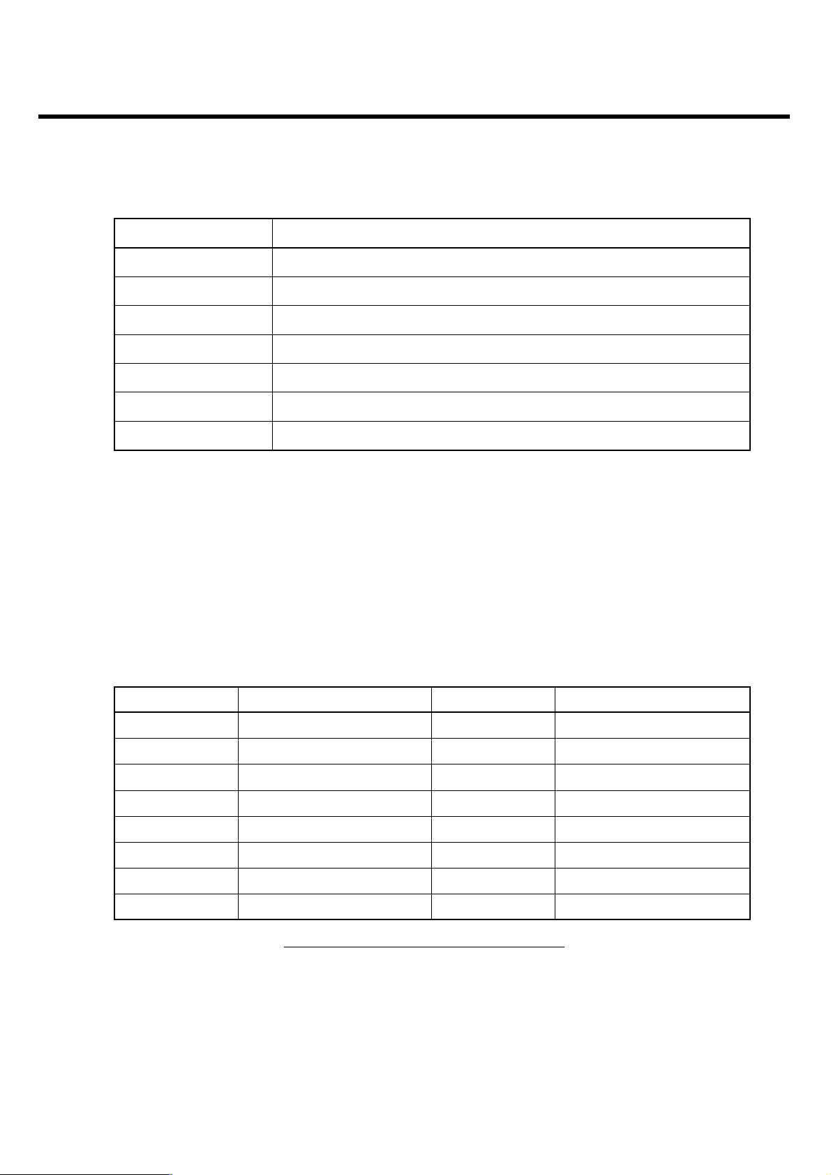
Item Specifications
Band GSM DUAL Band(900/1800)
Type Bar type
Dimension 101 * 46 * 12.9mm
Weight 65g
Battery 900mAh Li-ion
Talk Time
Up to 6.5 hrs @GSM900, TX Level : 10
Battery performance may vary depending on network and phone usage
Stand-by Time
Up to 630 hrs @Paging period : 9
Battery performance may vary depending on network and phone usage
RTC Under 1 minute when removed battery.
Antenna Internal Type(Dual-band)
LCD(Main) 1.52"(128x128 pixels), 65K Color STN LCD
KEY Back Light Yes
KEY Back Light color Blue
Vibrator Yes
Speaker&Receiver Yes(18x10 Dual Mode)
C-MIC Yes
Earphone Jack Mono or Stereo(Optional)
SIM Yes(Plug in Type) : 1.8V & 3.0V
MIDI 16 poly
I/O Connect 18 Pins (included Earphone Jack)
LGE Internal Use Only
Copyright © 2008 LG Electronics. Inc. All right reserved.
Only for training and service purposes
2.2 S/W Features
Function Detail Item Specification Etc.
Operating System OS O OSE
Data Circuit O
Packet X
Connectivity Infrared (IrDA) X
Bluetooth X
USB X
USB Mass storage X
RS232 O
Voice Function Voice Recording X
Voice Command X
Answering machine X
Memory User Memory O TBD Under 300KB
X MMS
X
Pictures (Still Image &
Moving Image)
X MP3 (Music Contents)
X Java Contents
O Wallpaper 3 bitmap images
O Ringtone 10 MIDI Ringtones
X external memory (microSD)
Camera Camera Module X
Audio Voice Codec O FR, HR, EFR, AMR-NB
AMR O
FM Radio O
Integrated handsfree speaker O Speaker phone mode
2. PERFORMANCE
- 8 -
LGE Internal Use Only
Copyright © 2008 LG Electronics. Inc. All right reserved.
Only for training and service purposes
Function Detail Item Specification Etc.
Display RSSI O 6 level
Battery Level O 5 level
RTC O
Multi Language O Basic:English
Max. 4 language of Latin
2 or 3 language of etc.
Quick Access Mode X
PLMN/Service Indicator O
Dimming Clock X
Dual Clock X
Local Time / Selected Area Time
Normal Features Last Dialed Number O 20
Last Received Number O 20
Last Missed Number O 20
Scratch Pad Memory X
Call Call Waiting O
Manage-ment Call Swap O
Call Retrieve O
Auto Answer X
Automatic Redial O
Calling Line identification O
Full Call divert O
Speed Dialing O
Last Number Redial O
Multi-party Call (Conference Call)
O
Explicit Call Transfer X
2. PERFORMANCE
- 9 -
LGE Internal Use Only
Copyright © 2008 LG Electronics. Inc. All right reserved.
Only for training and service purposes
2. PERFORMANCE
- 10 -
Function Detail Item Specification Etc.
Network Automatic Network Selection O
Manual Network Selection O
Network Service Status O
DTMF DTMF Signaling O
DTMF Enable & Disable O
Audio Key Tone Volume O 6 Level (Include Mute)
Ring Tone Volume O 6 Level (Include Mute)
Ring Tone Pattern O 10Type(fixed)
Ring Type Silent O Vibrator & Ring (Indicator)
Earpiece Volume O
6 Level (Include Mute)
Mute O
Cell Broadcast Read Cell Broadcast O
Cell Broadcast Categories O
Cell Broadcast Message O
Language
Phone Book Entry O 300
Field O Office, Mobile, Home
Numeric Store and Recall O
Alphabetic Store O
Alphabetic Recall O
Scroll by alphabetic or O
numeric order
Last Number Dialed
O20
Last Number Missed O 20
Last Number Received O 20
Copy & Move O
Fixed Dial Number O
Barred Dial Number X
Service Dial Number O
Email Entry X
Picture ID X
Video Caller ID X
My Name card X
LGE Internal Use Only
Copyright © 2008 LG Electronics. Inc. All right reserved.
Only for training and service purposes
2. PERFORMANCE
- 11 -
Function Detail Item Specification Etc.
Supp. Services Call Forwarding O All Incoming Calls,
O No Reply
O On Busy,
O Not reachable
Call Barring O All Outgoing Calls,
O International Calls,
O
Calls except to Home Country
incoming Calls,
O
All incoming Calls when roaming
Conference Call O up to 5 calls
SIM Plug?In Type O 1.8V & 3 V
SIM Lock O Service Provider / Network Lock
SIM Toolkit O Class 1, 2, 3
Prepaid SIM Operation O
Mega SIM X
Short Messaging Read Message O
Manage-ment Write and Edit Message O Not Support EMS
Send and Receive Message O
Reply to Message O
Forward Message O
Extract Number from Message O
Message Status O
Message Unread Indicator O
Settable Message Center Number,
O
Reply Path and Validity O
Visible and Audible Message
O
Receive Alerting
Voice Mail O
Settable Voice Mail Center Number
O
Message Protocol
O
Normal, Fax, National Paging,
Email, X400, ERMES, Voice
Message Overflow Indicator O
Message Center Number O
Help Menu X
LGE Internal Use Only
Copyright © 2008 LG Electronics. Inc. All right reserved.
Only for training and service purposes
2. PERFORMANCE
- 12 -
Function Detail Item Specification Etc.
Sound contents Ringtones O
Karaoke X
Stutter Sound X
Flip tone X
Button tone O
Others X
Miscellaneous Development & Test Facility O
Function Field Test Facility O
Display Software Version O
IMEI O
Text Input Language O Selectable Auto Language
Predictive word input O T9
Scheduler Schedule O 20 input (20 character)
To Do List X 50 input
Memo O 20 input (40 character)
D-day counter X
Send via Bluetooth X Schedule, Memo, To Do list, Messaging
World Time Setting Local Time O
Display Two Number of Cities Time X
Dual clock
Daylight saving X Summer time calibration function
NITS X Automatic setting as country code in SIM
Unit converter O Currency, Surface, Length, Weight,
Temperature, Volume, Velocity
Stop watch O
Calculator Calculation O + - * /
PC Sync Phone Book Sync X
Message Sync X
Multimedia Contents Sync O ringtone, wallpaper 1EA Download
Scheduler Sync X E-MAIL, EMS, Schedule, Phonebook,
Name card etc.
Sync ML DS X
DM X
Game O Sudoku support
Menu Quick Access Mode (Profile) X
External Interface Electrical Man Machine Interface O
Development and Test Facility O
LGE Internal Use Only
Copyright © 2008 LG Electronics. Inc. All right reserved.
Only for training and service purposes
2. PERFORMANCE
- 13 -
Function Detail Item Specification Etc.
Handset Restore Factory Setting O
Read Software Version O
Battery Charging Mode O
Security Emergency Call O
Handset Lock O
Security Code O Delete all
SIM Lock O
Key guard O
Real Time Clock 12/24 hour O
Calendar O
Automatic Leap Year Adjustment
Time Zone O
Daylight saving X
Alarm Manager O Once, Daily, Mon~Fri, Mon~Sat
Dimming Clock X
Power-off Alarm O
On Alarm Event O Display
Accessory Hand strap X
Embedded microSD Card X
microSD Adapter X
Stereo earmic O EarMic Type Provides optionally
only for supporting
FM radio function.
earmic w/music remote controller X
Neck strap X
LCD Cleaner X
Holster X
Data cable O RS232 cable Option
CD X
Holster charger X Standard battery Back-up
and Holster function
additional standard battery X
Extended Battery X
Desktop Charger X
Cigar Lighter Adapter X
Portable Handsfree X
Bluetooth headset X
Bluetooth stereo earset controller X
Car kit X
Leather Pouch X
Stylus Pen X
Luxury Package X
Compass X

- 14 -
3. TECHNICAL BRIEF
3.1 Digital Main Processor(PMB7880)
3. TECHNICAL BRIEF
LGE Internal Use Only
Copyright © 2008 LG Electronics. Inc. All right reserved.
Only for training and service purposes
Figure. 3-1 PMB7880 FUNCTIONAL BLOCK DIAGRAM

- 15 -
3. TECHNICAL BRIEF
3.1.1 Overview of E-GOLDvoice
The E-GOLDvoice is a GSM baseband modem including RF transceiver covering the low bands
GSM850 /GSM900 and high bands GSM1800 / GSM1900 bands.
E-GOLDvoice is Dual Band, therefore, it supports by default a low / high pair of bands at the same
time:
1. GSM850 / GSM1800
2. GSM850 / GSM1900
3. GSM900 / GSM1800
4. GSM900 / GSM1900
The E-GOLDvoice is optimized for voice-centric Mobile Phone applications.
The E-GOLDvoice is designed as a single chip solution that integrates the digital, mixed-signal, RF
functionality and a direct-to-battery Power Management Unit.
The transceiver consists of:
• Constant gain direct conversion receiver with an analog I/Q baseband interface
• Fully integrated Sigma/Delta-synthesizer capability
• Fully integrated two-band RF oscillator
• Two-band digital GMSK modulator with digital TX interface
• Digitally controlled crystal oscillator generating system clocks.
The E-GOLDvoice supports a direct battery connection, hence eliminating the need for an external
Power Management Unit. The E-GOLDvoice has different power down modes and an integrated
power up sequencer.
The E-GOLDvoice is powered by the C166®S MCU and TEAKLite® DSP cores. The operating
temperature range from -40°C to 85°C. It is manufactured using the 0.13 µm CMOS process.
LGE Internal Use Only
Copyright © 2008 LG Electronics. Inc. All right reserved.
Only for training and service purposes

LGE Internal Use Only
Copyright © 2008 LG Electronics. Inc. All right reserved.
Only for training and service purposes
3. TECHNICAL BRIEF
- 16 -
3.1.2 Features
] Baseband
• High performance fixed-point TEAKlite DSP
• C166S high performance microcontroller
• There are several Interfaces:
- I2S interface for DAI connections (for Tape Approval)
- High Speed SSC Interface for connection of external peripherals
- SIM Interface
- Keypad Interface (6x4 or 5x5 keys)
- EBU for external RAM/FLASH connection
- Asynchronous serial interface
- JTAG Interface
- Black & white and color displays are supported
- PWM source to drive vibrator
- Keypad and display backlight supported.
] Receiver
• Constant gain, direct conversion receiver with fully integrated blocking filter
• Two integrated LNAs
• No need of interstage and IF filter
• Highly linear RF quadrature demodulator
• Programmable DC output level
• Very low power budget.
] Transmitter
• Digital Sigma-Delta modulator for GMSK modulation, typical -163.5 dBc/Hz@20 MHz
• Single ended outputs to PA, Pout = +3.5 dBm
• Very low power budget.
] RF-Synthesizer
• Σ∆Synthesizer for multi-slot operation
• Fast lock-in times (< 150 µs)
• Integrated loop filter
• RF Oscillator
• Fully integrated RF VCO.
] Crystal Oscillator
• Fully digital controlled crystal oscillator core with a highly linear tuning characteristic.

- 17 -
3. TECHNICAL BRIEF
] Mixed Signal and Power Management Unit
• DC/DC boost for voltages up to 15V for driving White or Blue LEDs
• 8-Ohm loud speaker driver (250/350mW)
• 16-Ohm earpiece driver
• 32-Ohm headset driver
• 4 measurement interfaces (PA temperature, battery voltage, battery temperature,and ambient
temperature)
• Differential microphone input
• System start up circuitry
• Charger circuitry for NiCd, NiMh and LiIon cells
• Integrated regulators for direct connection to battery.
LGE Internal Use Only
Copyright © 2008 LG Electronics. Inc. All right reserved.
Only for training and service purposes

LGE Internal Use Only
Copyright © 2008 LG Electronics. Inc. All right reserved.
Only for training and service purposes
3.1.3 GSM System Description
The E-GOLDvoice is suited for mobile stations operating in the GSM850/900/ 1800/1900 bands.
In the receiver path the antenna input signal is converted to the baseband, filtered, and then amplified
to target level by the RF transceiver chipset.
Two A-to-D converters generate two 6.5 Mbit/s data streams. The decimation and narrowband channel
filtering is done by a digital baseband filter in each path.
The DSP performs:
1. The GMSK equalization of the received baseband signal (SAIC support available)
2. Viterbi channel decoding supported by an hardware accelerator.
The recovered digital speech data is fed into the speech decoder.
The E-GOLDvoice supports fullrate, halfrate, enhanced fullrate and adaptive multirate speech CODEC
algorithms.
The generated voice signal passes through a digital voiceband filter. The resulting 4 Mbit/s data
stream is D-to-A converted by a multi-bit-oversampling converter, postfiltered, and then amplified by a
programmable gain stage.
The output buffer can drive a handset ear-piece or an external audio amplifier, an additional output
driver for external loud speaker is implemented.
In the transmit direction the differential microphone signal is fed into a programmable gain amplifier.
The prefiltered and A-to-D converted voice signal forms a 2 Mbit/s data stream. The oversampled
voice signal passes a digital decimation filter.
The E-GOLDvoice performs speech and channel encoding (including voice activity detection (VAD)
and discontinuous transmission (DTX)) and digital GMSK modulation.
In the RF transceiver part, the baseband signal modulates the RF carrier at the desired frequency in
the 850 MHz, 900 MHz, 1.8 GHz, and 1.9 GHz bands using an I/Q modulator. The E-GOLDvoice
supports dual band applications.
Finally, an RF power module amplifies the RF transmit signal at the required power level. Using
software, the E-GOLDvoice controls the gain of the power amplifier by predefined ramping curves (16
words, 11 bits).
For baseband operation, the E-GOLDvoice supports:
• Making or receiving a voice call
• Sending or receiving an SMS.
3. TECHNICAL BRIEF
- 18 -

LGE Internal Use Only
Copyright © 2008 LG Electronics. Inc. All right reserved.
Only for training and service purposes
3. TECHNICAL BRIEF
- 19 -
3.1.4 PMU Details
The E-GOLDvoice includes battery charger support (various sensor connections for temperature,
battery technology, voltage, etc.) and a ringer buffer. E-GOLDvoice avoids the need for an external
power management component because its internal power management unit contains:
• Voltage regulators for the On-chip and Off-chip functional blocks
• Charger circuitry for NiCd, NiMh and LiIon cells.
3.1.5 Bus Concept
The E-GOLDvoice has two cores (a microcontroller and a DSP), each with its own bus.
There is an interconnection between the TEAKlite bus and the C166S X-Bus.
3.1.6 C166S Buses
The C166S is connected to three buses:
1. Local Memory (LM) bus
2. X-Bus
3. PD-Bus.
3.1.7 TEAKLite Bus
The TEAKlite is connected to the TEAKlite bus.
3.1.8 Bus Interconnections
The interconnection between the X-Bus and the TEAKlite Bus uses:
• Multicore Synchronization
• Shared Memory.
3.1.9 Clock Concept
The E-GOLDvoice has a flexible clock control.
3.1.10 Interrupt Concept
The C166 MCU carries out the E-GOLDvoice interrupt system.
3.1.11 Debug Concept
The E-GOLDvoice includes a multi-core debug. The C166 and TEAKlite cores can be debugged in
parallel with:
• A single JTAG port (that is, on a single host)
• Mutual breakpoint control.

LGE Internal Use Only
Copyright © 2008 LG Electronics. Inc. All right reserved.
Only for training and service purposes
3.1.12 C166 Debug Concept
The debugging of the C166 uses the OCDS and the Cerberus.
3.1.13 TEAKLite Debug Concept
TEAKlite debugging uses the OCEM and the SEIB.
3.1.14 Power Management
The E-GOLDvoice provides the power management unit (PMU) for the complete mobile phone
application. The integrated PMU is directly connected to the battery and provides a set of linear
voltage regulators (LDO’s).
These LDO’s generate all required supply voltages and currents needed in a low feature mobile
phone.
A charger control circuit charges NiCd, NiMH and LiIon batteries.
The charger control supports hardware controlled pre-charging and software controlled charging. It
offers a wide charger voltage range, making halfwave/full-wave charging with cheap transformers
possible. White/blue backlight generation is supported with a special driver for very a low external
parts count. Power consumption during operation phases is minimized due to flexible clock switching
In the Standby Mode most parts of the device are switched off, only a small part is running at 32kHz
and the controller RAM is switched to a power saving mode. The TEAKLite ROM can be switched off
during Standby via SW.
3.1.15 On-Chip Security Concept
Secure boot is based on a public/private key approach. Flash images that are not signed with the
private key during phone manufacture cannot be loaded.
Verification of the Flash code is done with the public key. The public key as well as hash and verify
algorithms are stored in the ROM, which ensures a hardware secured boot procedure.
The following security features are supported:
• Prevention of illegal Flash programming
• Flash programming makes use of the E-GOLDvoice ID for personalization checks with IMEI and
SIM-lock protection
3. TECHNICAL BRIEF
- 20 -

LGE Internal Use Only
Copyright © 2008 LG Electronics. Inc. All right reserved.
Only for training and service purposes
3. TECHNICAL BRIEF
- 21 -
The security features use the following mechanism:
• Boot ROM flow:
- Controls the boot transition to external flash
- Controls the flash update
• Flash tied to the individual chip via an ID using e-fuses, that is, each E-GOLDvoice chip has its
own fused ID.
Further details on the E-GOLDvoice security concept are not publicly documented.
3.1.16 Asynchronous Operation Mode Concept
The E-GOLDvoice can operate in either:
• The traditional synchronous mode with the 26MHz system clock synchronized on the base station
• A special asynchronous mode (XO concept).
In the asynchronous mode the 26MHz clock input is not synchronized with the base station; the
residual frequency offset is compensated in the digital signal processing domain. This processing
includes frequency and timing compensation of the baseband and voiceband signals.
LGE Internal Use Only
Copyright © 2008 LG Electronics. Inc. All right reserved.
Only for training and service purposes
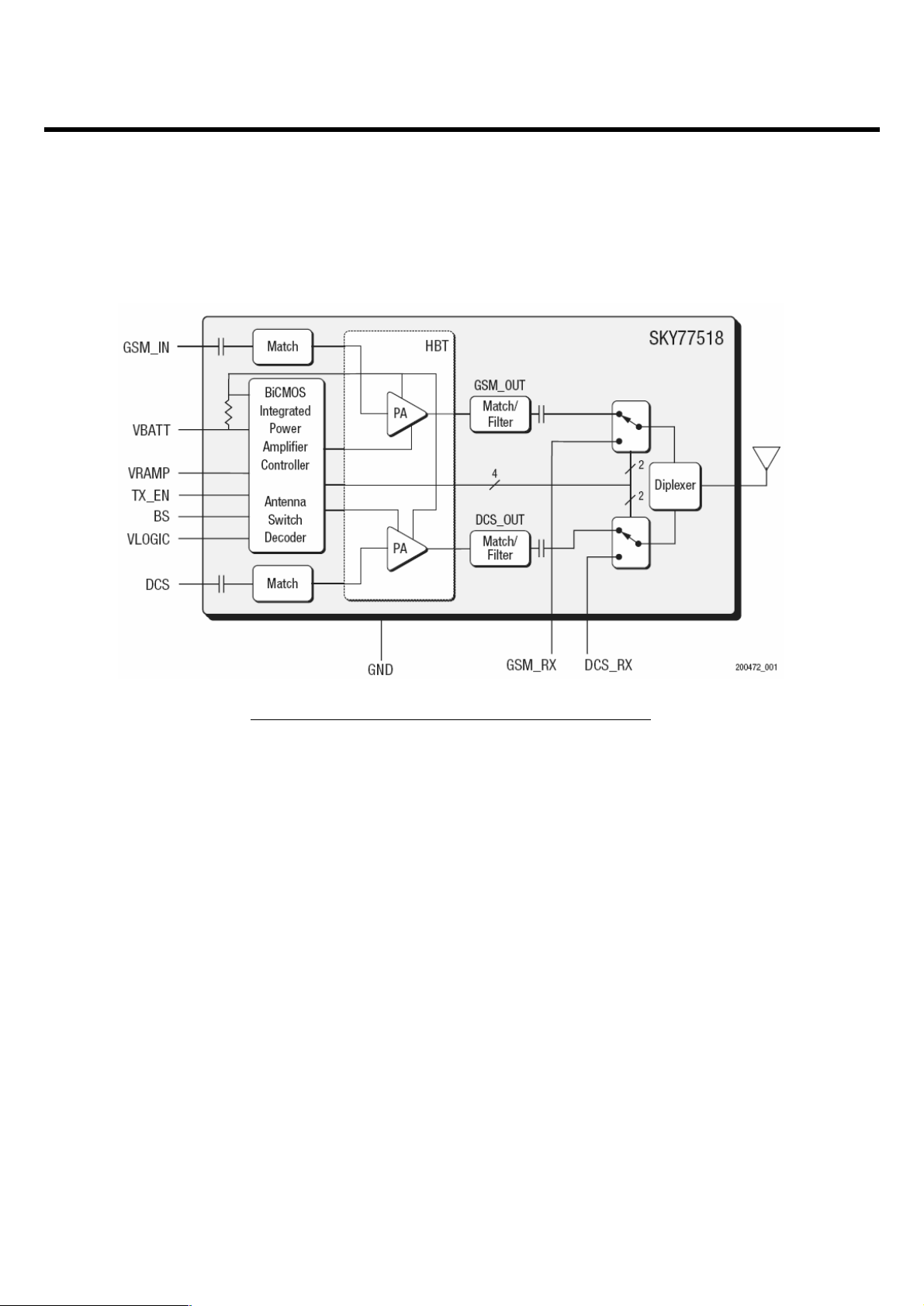
3.2 Power Amplifier Modul(SKY77518)
The SKY77518 is a transmit and receive front_end module(FEM) with integrated Power Amplifier
Control for dual_band cellular handsets comprising GSM900 and DCS 1800 Operation. Designed in a
low profile, compact form factor, the SKY77518 offers a complete transmit VCO-to Antenna and
Antenna-to-Receive SAW filter solution.
The module consists of a GSM900 PA block and a DCS1800 PA block, impedancematching circuitry
for 50ohm input and output impedances, Tx harmonics filtering, high linearity and low insertion loss
PHEMT RF switches, diplexer and a Power Amplifier Control (PAC) block with internal current sense
resistor. A custom BiCMOS integrated circuit provides the internal PAC function and decoder circuitry
to control the RF switches. The two Heterojunction Bipolar Transistor (HBT) PA blocks are fabricated
onto a single Gallium Arsenide (GaAS) die.
3. TECHNICAL BRIEF
- 22 -
Figure. 3-2 SKY77518 FUNCTIONAL BLOCK DIAGRAM

LGE Internal Use Only
Copyright © 2008 LG Electronics. Inc. All right reserved.
Only for training and service purposes
3. TECHNICAL BRIEF
- 23 -
One PA block supports the GSM900 band and the other PA block supports the DCS1800 band. Both
PA blocks share common power supply pads to distribute current.
The output of each PA block and the outputs to the two receive pads are connected to the antenna
pad through PHEMT RF switches and a diplexer. The GaAs ddie, PHEMT die, Silicon (Si)die and
passive components are mounted on a multi-layer laminate substrate. The assembly is encapsulated
with plastic overmold.
Band Selection and control of transmit and receive modes are performed using two external control
pads. Refer to the functional block diagram in Figure 3-2. The Band select pad (BS) selects between
GSM and DCS modes of peration. The transmit enable (TX_EN) pad controls receive or transmit
mode of the respective RF switch (TX = logic 1). Proper timing between transmit enable (TX_EN) and
Analog Power Control (VRAMP) allows for high isolation between the antenna and TX-VCO while the
VCO is being tuned prior to the transmit burst.
The SKY77518 is compatible with logic levels from 1.2V to VCC tor BS and TX_EN pads, depending
on the level applied to the VLOGIC pad. This feature provides additional flexibility for the designer in
the selection of FEM interface control logic.
LGE Internal Use Only
Copyright © 2008 LG Electronics. Inc. All right reserved.
Only for training and service purposes
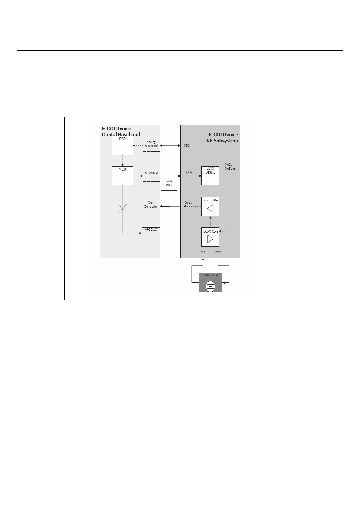
3.3 26 MHz Clock(DCXO)
DCXO (Digitally Controlled Crystal Oscillator) and VCTCXO (Voltage Controlled Temperature
Compensated Crystal Oscillator) are two different techniques used To maintain the mobile’s reference
oscillator’s accuracy over time. The reference oscillator’s accuracy over time will vary due to initial
crystal frequency offset, temperature drift and aging.
These static and dynamic frequency variations have to be compensated, otherwise the mobile would
be in danger of losing connection to the network. The technique used to perform the frequency
compensation is generally termed Automatic Frequency Control (AFC).
To summarize the operation of DCXO, GSM Baseband processor will calculate the AFC compensation
(which is continuously updated) required based on the measured frequency error. Then the required
AFC compensation is sent to the LUXO (Lineari-Zation Unit of Crystal Oscillator), which in turns
control the DCXO core and generates The 26MHz system clock.
3. TECHNICAL BRIEF
- 24 -
Figure. 3-3 E-GoldVoice DCXO Overview
LGE Internal Use Only
Copyright © 2008 LG Electronics. Inc. All right reserved.
Only for training and service purposes
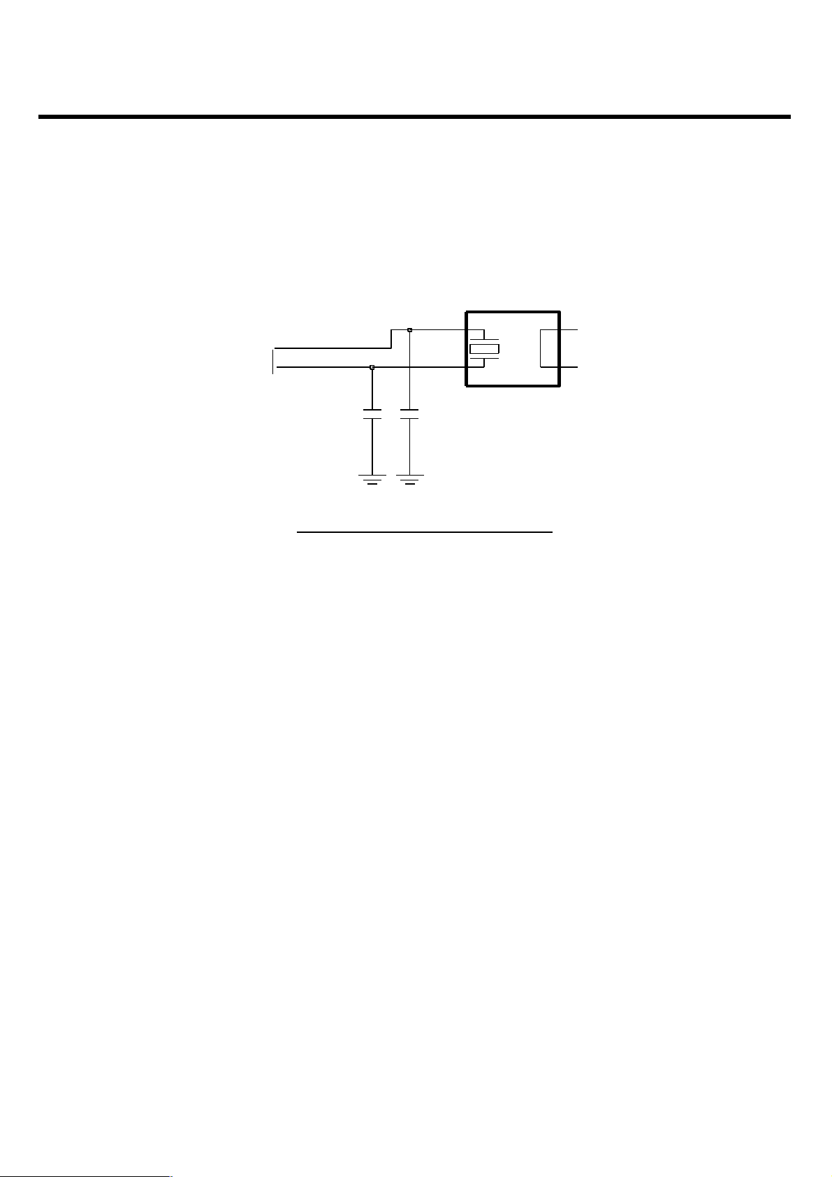
3.4 RTC(32.768KHz Crystal)
The integrated Real Time Clock (RTC) is able to provide programmable alarm functions and external
interrupts. Due to its extreme low power consumption the RTC can be supplied from a small backup
battery. This allows the generation of external interrupts, even when the main PMB7880 supply
voltage is switched off. For this purpose the RTC is powered by own voltage supply pins VDD_RTC
and VSS_RTC.
The RTC shall be driven by a 32.768 kHz (32k) clock which needs to be applied via the PMB7880
F32K and OSC32K pins. The clock can be fed from either an external clock source or use the on chip
32 KHz oscillator module.
The low clock frequency and the optimized low power design give the possibility to run the chip with a
minimum of power dissipation. For example, for this specific application the 26 MHz reference
oscillator can be switched off during system standby and a lowpower time reference can be kept when
the 32k clock is provided to the RTC.
The RTC consists of an PMB7880 specific RTC shell, containing the RTC macro, as well as the 32
kHz oscillator, as described in the following sections. The module RTC Shell solely performs level
translation of the 32KHz clock to the VDD_LD1 power supply domain, and is not functionally
associated with the RTC.
3. TECHNICAL BRIEF
- 25 -
Figure. 3-4 E-Gold Voice RTC Interface
C131
18p
OSC32K
F32K
R5
B4
X102
MC-146_12_5PF
12
3
4
32.768KHz
C132
18p
LGE Internal Use Only
Copyright © 2008 LG Electronics. Inc. All right reserved.
Only for training and service purposes
3.5 LCD Interface(3-wire SPI interface)
3. TECHNICAL BRIEF
- 26 -
Figure 3-5-1. LCD Interface
(ENQY0013801)
IMSA-9671S-13Y902
27p
C122
47R107
C126
NA
R111 47
R110 47
C125
27p
C124
NA
EVL5M02200
VA102
NA
R113
R112 47
2
3
4
5
6
7
8
9
CN101
14
15
1
10
11
12
13
C121
NA
2V8_VIO
C123
27p
VA101
EVLC5S0250
_LCD_CS
SSC0_MTSR
MLED1
MLED2
LCD_ID
MLED
LCD_RESET
SSC0_CLK
Figure 3-5-2. Charge pump interface
CHARGE PUMP
1u
C106
U101
C1+
10
9
C1-
7
C2+
6
C2-
CP
8
1
D1
D2
2
3
D3
EN_SET
11
GND
4
5
IN
NC
12
AAT3157ITP-T1
C101
1u
100K
R104
C103
NA1u
C102
C109
NA
C104
1u
C108
NA
VBAT
W_LED_DRV
MLED1
MLED2
MLED
LGE Internal Use Only
Copyright © 2008 LG Electronics. Inc. All right reserved.
Only for training and service purposes
The AAT3157 is a low noise, constant frequency charge pump DC/DC converter that uses a trimode
load switch (1X), fractional (1.5X), and doubling (2X) conversion to maximize efficiency for white LED
applications. The AAT3157 is capable of driving up to three channels of LEDs at 20mA per channel
from a 2.7V to 5.5V input.
The current sinks may be operated individually or in parallel for driving higher current LEDs. A low
external parts count (two 1µF flying capacitors and two small 1µF capacitors at VIN and VOUT) make
this part ideally suited for small, battery-powered applications. AnalogicTech's S2Cwire™ (Simple
Serial Control™) serial digital input is used to enable, disable, and set current for each LED with 16
settings down to 50µA.
The low-current mode supply current can be as low as 50µA to save power.
3. TECHNICAL BRIEF
- 27 -
Figure 3-5-3. Charge pump Output Current
Signals Description
_LCD_CS This signal enable to access to the driver IC of LCD.
SSC0_MTSR This signal transfer serial data to driver IC.
SSC0_CLK This signal transfer serial clock to driver IC.
LCD_RESET This signal makes driver IC to HW default status.
MLED This signal provide power to white LEDs.
MLED1/2 This signal be feed back from white LEDs.
2V8_VIO This signal provides power to LCD modules.(2.8V)
Data Output (mA/Ch) Data Output (mA/Ch)
1 20.0 9 5.0
2 17.0 10 4.2
3 14.0 11 3.4
4 12.0 12 2.8
5 10.0 13 1.0
6 8.6 14 0.5
7 7.0 15 0.1
8 6.0 16 0.05
LGE Internal Use Only
Copyright © 2008 LG Electronics. Inc. All right reserved.
Only for training and service purposes
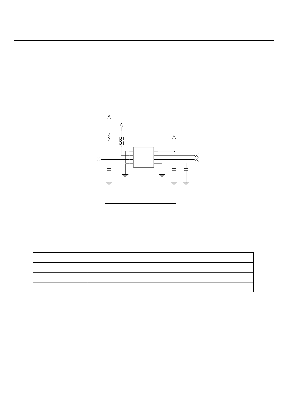
3.6 SIM Card Interface
The EGoldVoice provides SIM Interface Module. The AD6527 checks status Periodically During
established call mode whether SIM card is inserted or not, but it doesn't check during deep sleep
mode. In order to communicate with SIM card, 3 signals SIM_DATA, SIM_CLK, SIM_RST.
3. TECHNICAL BRIEF
- 28 -
Figure 3-6. SIM CARD Interface
SIM_CONNECTOR
0.1u
C134
22p
C133
2V85_VSIM
4.7K
R129
R130
0
2V85_VSIM
J101
3
CLK
GND
4
7
GND1GND2
8
6
I_O
RST
2
VCC
1
5
VPP
C135
22p
2V85_VSIM
SIM_DATA SIM_CLK
SIM_RST
Signals Description
SIM_RST This signal makes SIM card to HW default status.
SIM_CLK This signal is transferred to SIM card.
SIM_DATA This signal is interface datum.
LGE Internal Use Only
Copyright © 2008 LG Electronics. Inc. All right reserved.
Only for training and service purposes
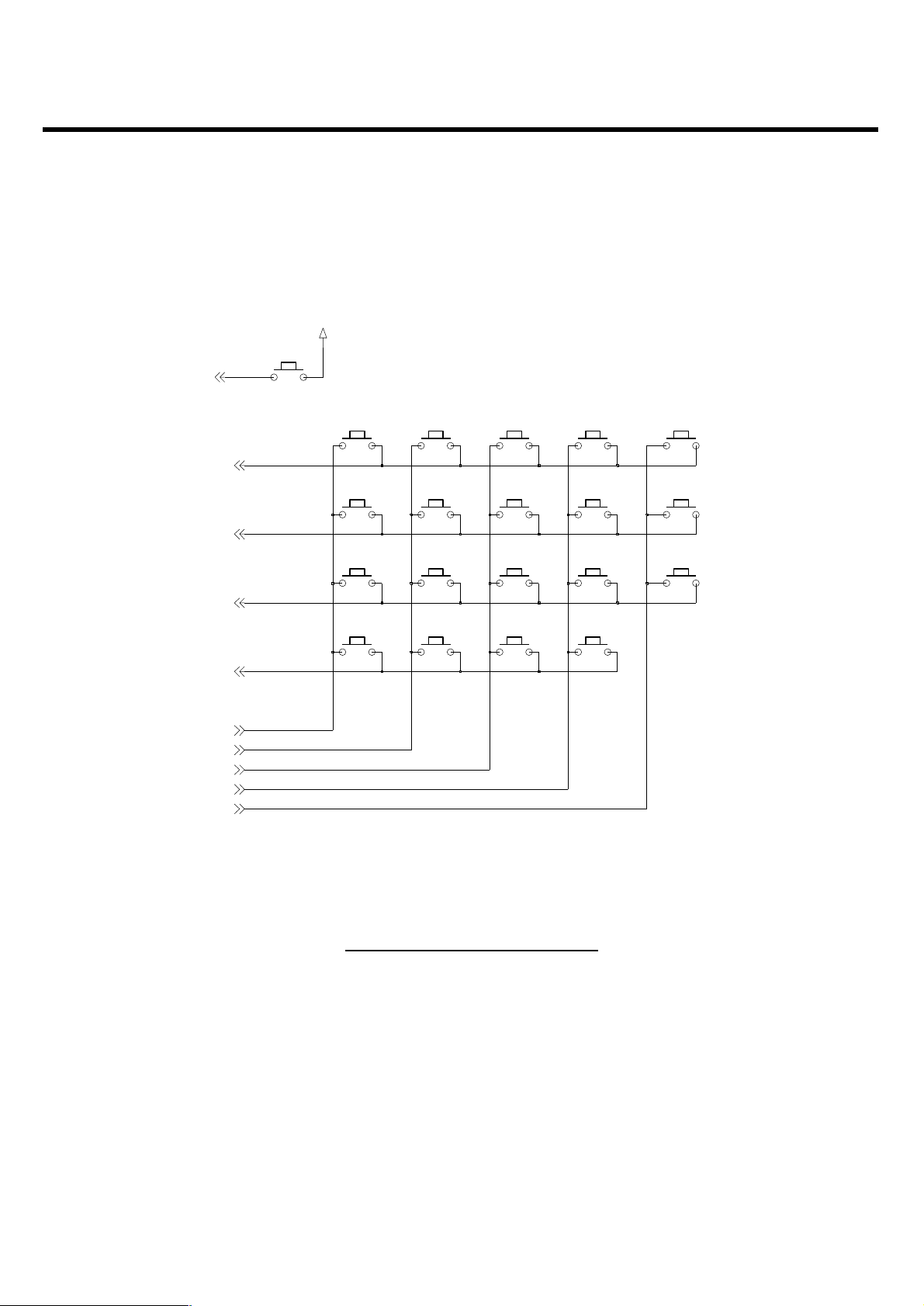
3.7 KEYPAD Interface
The keypad interface is connected to the X-Bus, together with the XBIU and the Shared Memory
Register, using a single Bus Interface.
The keypad supports two scan modes:
• By default, the keypad is a 4x6 scan matrix (4 input and 6 output pins).
• To set the keypad to a 5x5 scan matrix (5 input and 5 output pins)
The scan mode should be determined at the very beginning of the system start because changes are
not allowed later.
3. TECHNICAL BRIEF
- 29 -
Figure 3-7 KEY MAXTRIX Interface
5
RIGHT
2
LEFT
#
8
SEL
MENU
KEY MATRIX
END
9
4
0
UP
3
DOWN
*
6
SEND
7
1
SW305
2V0_VRTC
SW304
SW317
SW307
SW302 SW306
SW308
SW318
SW316
SW303
SW315SW312
SW319 SW320
SW313
SW301
SW309 SW311
SW310
SW314
KEY_IN3
KEY_OUT1
KEY_IN4
END_KEY
KEY_IN0
KEY_IN1
KEY_IN2
KEY_OUT4
KEY_OUT3
KEY_OUT2

LGE Internal Use Only
Copyright © 2008 LG Electronics. Inc. All right reserved.
Only for training and service purposes
3.8 Battery Charging Block Interface
The MP26021 is a linear, high-performance single cell Li-Ion battery charger. By integrating high
voltage input protection into the charger IC, the MP26021 can Tolerate an input surge up to 28V
The device features constant current (CC) and constant voltage (CV) charging modes with
programmable charge currents(85mA to 1A), programmable battery full threshold, thermal protection,
battery temperature monitoring, reverse current blocking and trickle charge. The device also provides
AC adapter power good and Charge status indications to the system.
MP26021 is available in a 10-pin 3mm x 3mm QFN package.
3. TECHNICAL BRIEF
- 30 -
Figure 3-8. Charging IC Interface
(1%)
(85mA)
(25V,K,Y5V)
(2012)
(1%)
(400mA)
(1608)
CHARGING IC
C129
2.2u
620
R123
47R121
R119
470K
VCHARGE
3.9K
R128
4.7u
C128
VBAT
U102 MP26021
10
BATT
6
GND
IBF
8
1
IN
9
ISET
5
NTC
PGND
11
SS
7
3
_ACOK
_CHG
2
_EN
4
1.8KR120
R125
100K
20K
R127
R126
100K
0.1u
C130
CHG_EN
CHARGE_DETECT
LGE Internal Use Only
Copyright © 2008 LG Electronics. Inc. All right reserved.
Only for training and service purposes
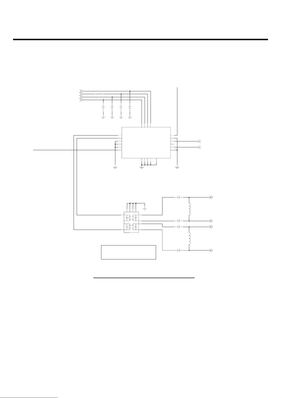
3.9 RF Interface
E-GOLDvoice features a fully integrated constant-gain direct conversion receiver, i.e. there is no
interstage filter needed and the baseband level at the analogue IQinterface follows directly the RF
input level. Depending on the baseband ADC dynamic range, single- or multiple-step gain switching
schemes are possible.
An integrated, selfaligning, low-pass filter ensures the receivers to function under blocking and
reference interference conditions and avoids aliasing by baseband sampling. An automatic DC-offset
compensation is implemented and can be switched depending on the gain setting.
3. TECHNICAL BRIEF
- 31 -
Figure 3-9-2. RF Module /SAW Filter interface
7
GSM_RX
NC
18
21
PGND
TX_EN
4
1
VBATT
VLOGIC
2
3
VRAMP
PCS_IN
19
6
PCS_RX
17
11
ANT
5
BS
GND1
8
9
GND2
10
GND3
GND4
12
13
GND5
GND6
14
15
GND7
GND8
16
GND9
20
GSM_IN
IN CASE OF GSM850/PCS1900
TO PART_NO SFSB0001301
PART_NO SFSB0001401
CHANGE THIS DUAL SAW FILTER
5.1nH
L405
1K R405
39p
C409
39p
C411
2G13G25G310
G4
I1
1
I2
4
9
O1_1
O1_2
8
O2_1
7
O2_2
6
B9310FL401
C414 3p
3pC416
SKY77517
U401
L404
18nH
C408
39p
3pC413
C415 3p
C410
39p
VLOGIC
DCS_PCS_OUT
GSM_OUT
GSM_RXN
GSM_RXP
DCS_RXN
DCS_RXP
BS
TXON_PA
TX_RAMP

LGE Internal Use Only
Copyright © 2008 LG Electronics. Inc. All right reserved.
Only for training and service purposes
The digital transmitter architecture is based on a fractional-N sigma-delta synthesizer for constant
envelope GMSK modulation. This configuration allows a very low power design with a reduced
external component count.
The modulation is transferred between baseband- and RF-part of the PMB7880 via a digital interface
signal into the digital modulator. The following Gaussian filter shapes the digital data stream for the
GMSK modulation. Additionally a pre-distortion filter compensates the attenuation of the PLL transfer
function resulting in a very low distortion at the transmit output.
The filtered digital data stream is scaled appropriately and added to the channel word.
This sum is fed into the MASH modulator. The output of the MASH modulator is a sequence of integer
divider values representing the high resolution fractional input signal. This sequence controls the MMD
(multi modulus divider) at a sample rate of 26MHz. Thus a tightly controlled frequency modulation of
the VCO is achieved.
3. TECHNICAL BRIEF
- 32 -
 Loading...